New application of AIEgens realized in photodetectors: reduced work function of transparent electrodes and much improved performance†
Lei
Feng‡
a,
Can
Wang‡
 b,
Xianyu
Deng
 *a,
Xincheng
Miao
a,
Jiaqiang
Wang
b,
Yangyang
Wang
a and
Zhen
Li
 *b
*b
aResearch Center for Advanced Functional Materials and Devices, Shenzhen Key Laboratory of Advanced Materials, School of Materials Science and Engineering, Harbin Institute of Technology, Shenzhen, 518055, P. R. China. E-mail: xydeng@hit.edu.cn
bDepartment of Chemistry, Wuhan University, Wuhan 430072, China. E-mail: lizhen@whu.edu.cn
First published on 10th October 2017
Abstract
Highly sensitive organic photodetectors were achieved by tuning the work function of transparent electrodes using two AIEgens with different ionic side chains. With the insertion of AIE molecules, their projected detectivity (D*) was enhanced by over one order of magnitude, which was accompanied by a fast response speed and a large linear dynamic range. The devices exhibited the ability to effectively detect weak light with intensity less than 10 pW cm−2, which is clearly superior to traditional silicon photodetectors. The AIE molecules developed a good energetic match to facilitate photocurrents, and the non-conjugated ionic impeding effect blocked the electrons from transferring to the interface under dark conditions and lower dark currents, which significantly contributed to the high detectivity of the devices. This study indicates that high performance organic devices could be achieved by jointly controlling conjugation associated aggregation and the quantity and state of ions on the electrode surface, thus providing a new application for AIEgens.
As a basic device to convert light into an electrical signal, photodetectors exhibit great potential in various important applications, such as photoswitches, probes, imaging, and communications.1–5 Nowadays, the rapid development of organic-based optoelectronic devices such as organic light emitting diodes (OLEDs) and organic solar cells (OSCs) has attracted increasing attention particularly to organic photodetectors (OPDs). In particular, recent reports show that OPDs are superior in various aspects than the commonly used photodetectors based on inorganic materials, such as they have a wide variety of sources, high throughput solution processing as well as flexible, large-scale, and high resolution device fabrication.6–10
Although the process of converting light to electricity in organic diode photodetectors is similar to that in organic solar cells, the mechanism and parameters, specifically in these devices, are very different. Moreover, unlike solar cells which only work under the blazing sun and with a large current, photodetectors generally work under very weak illumination and a very small current signal. Furthermore, the device stability of OPDs compared with light-emitting diodes and solar cells is less of a concern. Although the detectivity of OPDs has reached a high level, their response speed, linear dynamic range (LDR) and stability are still issues for commercial applications. Previous reports have mainly focused on the performance improvement of OPDs by studying materials with new structures,11–14 while relatively few researchers have paid attention to electrode engineering.
Electrode interfacial engineering is also an important approach to enhance the performance of organic photodetectors.15–17 In traditional organic opto-electronic devices, a transparent film, such as indium tin oxide (ITO), is generally used as a window electrode for the anode. However, the bottom electrode of ITO, used as the cathode, has been considered more suitable for both high efficiency and long-term stability than the traditional forward structure because there is no active metal involved in the device. One key problem of ITO as the cathode is that its high work-function is largely mismatched with the energy level of organic active materials. To solve this problem, several methods have been used in previously reported OSCs and OLEDs. These typically include covering ITO with a neutral insulating polymer of PIEI,18 the conjugated polymer electrolyte of PFN,19 the zwitterions of dyes,20 and the natural biomaterials amino acids and peptides.21,22 Since ITO is negatively charged, Chen et al. used the cathodic molecules and anodic molecules for the modification of ITO, layer by layer, to control its work function to fabricate inverted polymer solar cells with long-term stability.23
Since the concept of “aggregation induced emission” (AIE) was coined by Ben Zhong Tang in 2001, it has become a hot topic in the field of advanced functional materials.24 Due to the great efforts of scientists, AIEgens have been rationally designed for possible applications in OLEDs as emissive/host materials, as chemo and bio-sensors for highly sensitive detection or bioimaging, and others. However, interestingly, there were no reports concerning the utilization of AIEgens as electrode interfacial materials except the study reported by our group based on OSC25 despite their unique molecular packing and conjugation derived from their twisted conformation, in addition to the present non-conjugated PEO and PIEI and conjugated polymer electrolyte of PFN.
In this study, two AIEgens, WC-1 and WC-2, with different ionic side chains were employed to tune the surface work function of ITO via a simple solution process. The AIE molecule modified transparent electrodes were used as the electron selective layer for wideband organic-based photodetectors (OPDs), which resulted in a significantly higher projected detectivity (D*), faster response time, and large linear dynamic range (LDR). Herein, we present the device fabrication and photodectivity performance in detail.
Results and discussions
The chemical structure of the AIEgens and device structure of the OPDs are shown in Fig. 1. As shown in the figure, WC-1 possesses one ionic chain, whereas WC-2 possesses two. The highly twisted conformation of the TPE (tetraphenylethylene) moiety did not allow any intermolecular interactions in WC-1 and WC-2, although they are aromatic compounds. Thus, these types of molecules possess aromatic groups similar to PFN, but without the intermolecular-interactions such as those observed in PEO and PIEI, which possibly led to some interesting results. The active layer is composed of a blend of poly[4,8-bis(5-(2-ethylhexyl)thiophen-2-yl)benzo[1,2-b;4,5-b′]dithiophene-2,6-diyl-alt-(4-(2-ethylhexyl)-3-fluorothieno[3,4-b]thiophene-2-carboxylate-2-6-diyl)] (PCE-10 or PTB7-Th) and [6,6]-phenyl C61-butyric acid methyl ester (PC61BM). Fig. 2a shows the absorbance spectra of PCE10, PC61BM and the blend of PCE-10:PC61BM. The active layer has a wide response covering the ultraviolet (UV) to near-infrared (NIR) region with wavelengths ranging from 350 to 800 nm. Fig. 2b exhibits the external quantum efficiency (EQE) of the device at −0.1 V, which has a photo-response consistent with the absorbance spectrum shown in Fig. 2a. As shown in Fig. 2b, the EQE of the devices increased for the entire photo-response wavelength range after each AIE molecular modification. Fig. 2c shows the current–voltage (J–V) characteristics of the OPDs with WC-1 and WC-2 under dark conditions. For the samples with the AIE molecule modifications, there was a significant reduction in their dark current density (Jd) for voltages ranging from −2.0 to 2.0 V. In particular to the WC-2 modification, the Jd decreased by over one order of magnitude in the entire test voltage range. At close to 0 V, the Jd clearly decreased from 10−8 to 10−10 A cm−2 for both the WC-1 and WC-2 modifications. Thus, as shown in Fig. 2d, the projected detectivity (D*) of the devices with WC-1 and WC-2 at −0.1 V was higher than that of the device with bare ITO. The device with the modification exhibited a remarkable D* of over 1012 Jones in the entire wavelength range from 350 to 800 nm. Fig. 3 compares the actual detection ability of traditional Si photodetectors and the OPDs with AIE molecules at different voltages, which implies that the actual detectivity of the OPD is higher than that for traditional Si photodetectors and is over 1011 Jones.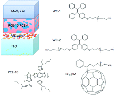 | ||
| Fig. 1 Schematic of the organic photodetector (OPD) device architecture and chemical structure of the AIE and active layer materials. | ||
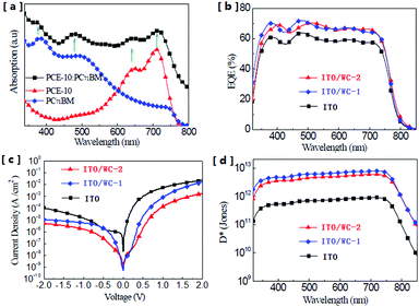 | ||
| Fig. 2 (a) Absorption spectra of the active layer materials. (b) External quantum efficiency of the OPDs with and without AIE molecules. (c) Current density–voltage (J–V) characteristics of the OPDs measured under dark conditions. (d) Projected detectivity (D*) of the OPDs at a bias of −0.1 V. The concentration of the solutions for the modification was 1.5 mg mL−1 for WC-1 and 0.75 mg mL−1 for WC-2. The device performance was optimized by tuning the concentration of the WC-1 and WC-2 solutions for use in the ITO modification. The EQE of the devices fabricated by ITO modification with different concentrations of WC1 and WC-2 solutions is shown in the ESI† (Fig. S1 and S2). | ||
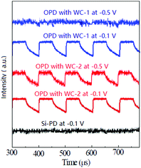 | ||
| Fig. 3 Signal from the oscilloscope for the Si and organic based photodetectors at different voltages under a 550 nm light source with an intensity of 10 pW cm−2. | ||
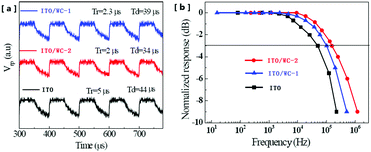
The response speed of OPDs is a very important parameter in various optoelectronic applications. Fig. 4a shows the time-resolved photoresponse voltages (Vrp), where the illumination was provided by an infrared laser source driven by a rectangular wave voltage pulse. As shown in Fig. 4a, the device with ITO exhibits a rise time (Tr) of 5 μs and a decay time (Td) of 44 μs, whereas that for the devices with WC-1 and WC-2 are 2.3 μs and 39 μs, and 2.0 μs and 34 μs, respectively. The Tr and Td are reduced by 60% and 23%, respectively, after the ITO modification with WC-2. With a corresponding result, the device with pristine ITO exhibits a −3 dB bandwidth of 103 kHz, whereas the −3 dB bandwidths of the devices with WC-1, and WC-2 are 130 kHz and 156 kHz (Fig. 4b), respectively.
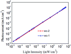
The plot in Fig. 5 shows that the photodetector has a linear response to light intensity that varies from 1 × 10⁻⁵ to 102 mW cm−2, which corresponds to a linear dynamic range (LDR) of 70 dB. The measured LDR is generally limited by the test conditions. The theoretical value of the LDR was calculated according to the following equation:26
LDR = 20![[thin space (1/6-em)]](https://www.rsc.org/images/entities/char_2009.gif) log(Jph*/Jd) log(Jph*/Jd) | (1) |
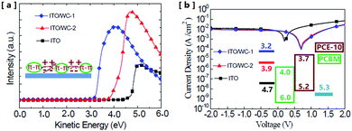
To investigate the original mechanism of the AIE molecules and its influence on the performance enhancement, the change in the surface work function of ITO was measured via ultra-violet photoemission spectroscopy (UPS). The UPS measurements indicate that after the modification with the AIE molecules, the surface work function of ITO exhibits a significant reduction. Fig. 6a shows the work function change in the ITO surface through modifications, which was characterized by the UPS spectra of ITO with or without the AIEgens. As shown in Fig. 6a, the original work function of ITO is about 4.7 eV, which significantly reduced to 3.9 and 3.2 eV after the ITO was covered with WC-2 and WC-1, respectively. The reduction of the work function can effectively improve the energetic match between the electrode and the organic active layer. First, the work function reduction of ITO would enlarge the work function difference between the anode and cathode of the device, which will enhance the build-in electric field to obtain a high open circuit voltage (Voc).28,29Fig. 6b shows the photocurrent vs. voltage plots of the devices with and without the AIE molecule modifications. It shows that the Voc increases from 0.25 to 0.75 V after the two modifications. The Voc of the two devices with WC-1 or WC-2 is almost the same due to the limitation of the energetic gap between the two levels, the lowest unoccupied molecular orbits (LUMO) of PC61BM and highest occupied molecular orbits (HOMO) of PCE-10.30 This is consistent with the energy level scheme shown in the inset of Fig. 6b. The ionic number in the molecular structure of WC-2 is higher than that of WC-1. A greater amount of ions decreases the aggregation effect of the molecules, which indicates that the aggregation state also plays an important role in the change in work function. The device with WC-2 exhibits the lowest dark current at high voltages, which could be attributed to its more insulative ionic side chains.
In previous reports, the action mechanism of polymers or organic molecules as an interfacial material was complicated and not clearly defined due to various influencing factors, such as molecule polarity, surface state and density. Unlike the common π-conjugated CILs, in which its molecules are assembled by the joint effect of strong π–π stacking interactions and van der Waals interactions, the twisted aromatic core of AIE CILs eliminates the possibility of π–π stacking and provides weak intermolecular interactions. Therefore, the strong van der Waals interactions of the polar side chains play a dominant role in the assembling behavior of AIE molecules on the interface between the active layer and cathode. This leads to the construction of well-organized structures such as the lamellar stacking pattern of WC-2 along the vertical orientation in the device, which is beneficial for electron transport. Similar consideration has also been reported in other studies.31–34 These results could effectively explain the significant reduction in the dark current density, which contributes to the large enhancement in detectivity.
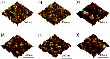
Another effect of the modification is to change the surface characteristics of both the ITO and the organic active layer. To investigate the effect of the AIEgens on the morphology of the ITO surface, we conducted AFM measurements on ITO substrates with and without AIE molecules. The AFM images in Fig. 7a to c illustrate that the roughness values of the bare ITO, WC-1 covered ITO, and WC-2 covered ITO are 2.41, 0.51, and 1.45 nm, respectively, indicating that the modification slightly decreased the roughness of the ITO surface. We also compared the morphology of PCE-10:PC61BM films that were spin-coated on the ITO substrate with and without WC-1 or WC-2. As shown in Fig. 7d to f, the roughness values of the PCE-10:PC61BM films on the original ITO, WC-1 modified ITO, and WC-2 modified ITO are 2.25, 1.36, and 1.22 nm, respectively, indicating that the modification of ITO also slightly reduced the surface roughness of the organic active layer.
Experimental
Materials
WC-1 and WC-2 were synthesized according to the methods described our previous report.34 PCE-10 and PC61BM were purchased from Solarmer Energy. Inc. and Sigma-Aldrich®, respectively. Indium–tin–oxide (ITO) glass substrates (7–10 Ω per square) were purchased from CSG Holding Co., Ltd.Device fabrication
ITO was ultrasonically cleaned using acetone, alkaline lotion, de-ionic water and isopropanol, in sequence. Then, 1.5 mg mL−1 WC-1 or 0.75 mg mL−1 WC-2 methyl solution was spin-coated at a speed of 4000 rpm on the surface of ITO. The prepared substrates were spin-coated with a solution of 10 mg mL−1 PCE-10 and 20 mg mL−1 PC61BM in chlorobenzene with the additive 1,8-diiodooctane (DIO) (3% v/v) at a speed of 1500 rpm for 60 s. The thickness of the active layer was about 200 nm. Finally, a 10 nm thick MoO3 layer and a 120 nm thick Al layer were deposited on top of the active layer as the anode.Device characterization
A commercial laser diode with a wavelength of 780 nm (RLD78MYA1, ROHM) was used as the infrared light source for the measurement of the detector performance. For the Voc measurement, a solar simulator was used as the light source with the intensity of 100 mW cm−2 at AM1.5. The photocurrent under luminance was recorded by a Keithley 2400 source meter, whereas the dark current was recorded by a Keithley 4200 source meter with the samples placed in a metal shielding box. The external quantum efficiency (EQE) was recorded by a quantum efficiency (QE)/IPCE measurement system (SR830, Stanford Research Systems).Transient response measurement
A waveform generator (33220A, Agilent) was used to drive the laser diode to output a square pulse light. A 100 MHz digital oscilloscope (TDS 1012C-SC, Tektronix) was used to record the photocurrent from the OPDs.Linearity measurement
A Keithley 2400 source measurement unit was used to record the photocurrent of the OPDs. A light source with an intensity ranging from 1 μW cm−2 to 100 mW cm−2 was provided by the laser diode when driven with different voltages.UV-vis, AFM, and UPS measurement
UV-visible absorption spectra were recorded using a UV-vis-NIR spectrophotometer (SHIMADZU UV 3600). AFM was performed using a Bruker Icon AFM. An unfiltered HeI (21.2 eV) gas discharge lamp and a total instrumental energy resolution of 0.1 eV were used to characterize the valence states and the vacuum level (VL) for the UPS measurement. The Fermi level (EF) was referenced as the zero binding energy (BE). Both the UPS and XPS measurements were performed at room temperature.Related calculations
If the shot noise is the main noise that roots in dark current, the projected detectivity (D*) was calculated using the following equation:where, D* is the detectivity in cm Hz1/2 W−1 or Jones; Rλ is the responsivity in A W−1, which can be calculated from the EQE value; Jd is the dark current density of the OPDs in A cm−2.
Considering the experimental noise, the value of D* is determined using the following equation:
The −3 dB bandwidth (f−3dB) was calculated according to the following equation:
Conclusions
In summary, the surface work function of a transparent electrode was tuned by two AIE molecules with different ionic side chains. With the adjusted work function of the ITO surface, the detectivity was enhanced by one order of magnitude up to 8.67 × 10¹² Jones at −0.1 V and 750 nm. The organic photodetectors exhibit remarkably high detectivity of over 1012 Jones in a wide wavelength range from UV to near-infrared (350 nm to 800 nm) at −0.1 V as the result of a very low dark current (lower than 1 nA cm−2). The devices exhibit the ability to effectively detect weak light with intensity less than 10 pW cm−2, which is clearly superior to traditional silicon photodetectors. In addition to their significantly enhanced detectivity, the response time of the photodetectors is apparently shortened. The photodetectors also exhibit a wide linear dynamic range. These results show that ionic AIE molecules are important materials for tuning the work function of electrode surfaces to enhance the performance of organic photodetectors, thus providing a novel and interesting pathway to develop interfacial materials for high performance organic electrical devices. Due to the special, sometimes even unique properties of AIEgens,35,36 their utilization in photodetector devices might open up a new avenue for AIEgens.Conflicts of interest
There are no conflicts to declare.Acknowledgements
We acknowledge financial support from the NSFC (No. 21674031, 21325416).Notes and references
- F. H. L. Koppens, T. Mueller, P. Avouris, A. C. Ferrari, M. S. Vitiello and M. Polini, Nat. Nanotechnol., 2014, 9, 780–793 CrossRef CAS PubMed
.
- G. Konstantatos and E. H. Sargent, Nat. Nanotechnol., 2010, 5, 391 CrossRef CAS PubMed
.
- X. Gong, M. Tong, Y. Xia, W. Cai, J. S. Moon, Y. Cao, G. Yu, C. L. Shieh, B. Nilsson and A. J. Heeger, Science, 2009, 325, 1665 CrossRef CAS PubMed
.
- T. Agostinelli, M. Campoy-Quiles, J. C. Blakesley, R. Speller, D. D. C. Bradley and J. Nelson, Appl. Phys. Lett., 2008, 93, 203305 CrossRef
.
- S. Kim, Y. T. Lim, E. G. Soltesz, A. M. De Grand, J. Lee, A. Nakayama, J. A. Parker, T. Mihaljevic, R. G. Laurence, D. M. Dor, L. H. Cohn, M. G. Bawendi and J. Frangioni, Nat. Biotechnol., 2004, 22, 93 CrossRef CAS PubMed
.
- Y. Zhang, Y. B. Yuan and J. Huang, Adv. Mater., 2017, 29, 1603969 CrossRef PubMed
.
- R. Nie, X. Deng, L. Feng, G. Hu, Y. Wang, G. Yu and J. B. Xu, Small, 2017, 13, 1603260 CrossRef PubMed
.
- X. Zhou, D. Yang, D. Ma, A. Vadim, T. Ahamad and S. M. Alshehri, Adv. Funct. Mater., 2016, 26, 6619 CrossRef CAS
.
- L. Shen, E. Y. B. Pun and J. C. Ho, Mater. Chem. Front., 2017, 1, 630–645 RSC
.
- J. Xiao, H. Yang, Z. Yin, J. Guo, F. Boey, H. Zhang and Q. Zhang, J. Mater. Chem., 2011, 21, 1423–1427 RSC
.
- S. Li, X. Deng, L. Feng, X. Miao, K. Tang, Q. Li and Z. Li, Polym. Chem., 2017, 8, 1039 RSC
.
- X. Wang, L. Lv, L. Li, Y. Chen, K. Zhang, H. Chen, H. Dong, J. Huang, G. Shen, Z. Yang and H. Huang, Adv. Funct. Mater., 2016, 26, 6306 CrossRef CAS
.
- L. Z. Zhang, T. B. Yang, L. Shen, Y. J. Fang, L. Dang, N. J. Zhou, X. G. Guo, Z. R. Hong, Y. Yang, H. B. Wu, J. S. Huang and Y. Y. Liang, Adv. Mater., 2015, 27, 6496 CrossRef CAS PubMed
.
- Y. Wu, Z. Yin, J. Xiao, Y. Liu, F. Wei, K. J. Tan, C. Kloc, L. Huang, Q. Yan, F. Hu, H. Zhang and Q. Zhang, ACS Appl. Mater. Interfaces, 2012, 4, 1883–1886 CAS
.
- R. Nie, Z. Zhao and X. Deng, Synth. Met., 2017, 227, 163 CrossRef CAS
.
- S. Wu, B. Xiao, B. Zhao, Z. He, H. Wu and Y. Cao, Small, 2016, 12, 3374 CrossRef CAS PubMed
.
- E. Saracco, B. Bouthinon, J.-M. Verilhac, C. Celle, N. Chevalier, D. Mariolle, O. Dhez and J.-P. Simonato, Adv. Mater., 2013, 25, 6534 CrossRef CAS PubMed
.
- Y. Zhou, C. Fuentes-Hernandez, J. Shim, J. Meyer, A. J. Giordano, H. Li, P. Winget, T. Papadopoulos, H. Cheun, J. Kim, M. Fenoll, A. Dindar, W. Haske, E. Najafabadi, T. M. Khan, H. Sojoudi, S. Barlow, S. Graham, J. L. Bredas, S. R. Marder, A. Kahn and B. Kippelen, Science, 2012, 336, 327 CrossRef CAS PubMed
.
- Z. He, C. Zhong, S. Su, M. Xu, H. Wu and Y. Cao, Nat. Photonics, 2012, 6, 591 Search PubMed
.
- K. Sun, B. M. Zhao, A. Kumar, K. Y. Zeng and J. Y. Ouyang, ACS Appl. Mater. Interfaces, 2012, 4, 2009 CAS
.
- R. Nie, A. Li and X. Deng, J. Mater. Chem. A, 2014, 2, 6734 CAS
.
- X. Deng, R. Nie, A. Li, H. Wei, S. Zheng, W. Huang, Y. Mo, Y. Su, Q. Wang, Y. Li, J. Tang, J. Xu and K.-Y. Wong, Adv. Mater. Interfaces, 2014, 1, 1400215 CrossRef
.
- B. Jiang, Y. Peng and C. Chen, J. Mater. Chem. A, 2017, 5, 10424 CAS
.
- J. Mei, N. L. C. Leung, R. T. K. Kwok, J. W. Y. Lam and B. Z. Tang, Chem. Rev., 2015, 115, 11718 CrossRef CAS PubMed
.
- C. Wang, Z. Liu, M. Li, Y. Xie, B. Li, S. Wang, S. Xue, Q. Peng, B. Chen, Z. Zhao, Q. Li, Z. Ge and Z. Li, Chem. Sci., 2017, 8, 3750–3758 RSC
.
- Z. H. Sun, Z. K. Liu, J. H. Li, G.-A. Tai, S.-P. Lau and F. Yan, Adv. Mater., 2012, 24, 5878 CrossRef CAS PubMed
.
- M. A. Khan, J. Kuznia, D. Olson, J. Van Hove, M. Blasingame and L. Reitz, Appl. Phys. Lett., 1992, 60, 2917 CrossRef CAS
.
- X. Deng, W. Lau, K. Wong, K. Low, H. Chow and Y. Cao, Appl. Phys. Lett., 2004, 84, 3522 CrossRef CAS
.
- Y. Cao, G. Yu and A. J. Heeger, Adv. Mater., 1998, 12, 917 CrossRef
.
- S. Zhang, L. Ye, W. Zhao, D. Liu, H. Yao and J. Hou, Macromolecules, 2014, 47, 4653 CrossRef CAS
.
- Z. Xie, V. Stepanenko, B. Fimmel and F. Wurthner, Mater. Horiz., 2014, 1, 355 RSC
.
- H. Zhao, Y. Luo, L. Liu, Z. Xie and Y. Ma, Mater. Chem. Front., 2017, 1, 1087 RSC
.
- C. Gu, C. Jia and X. Guo, Mater. Chem. Front., 2017, 1, 2125 RSC
.
- P. Y. Gu, Z. Wang, F. X. Xiao, Z. Lin, R. Song, Q. F. Xu, J. M. Lu, B. Liu and Q. Zhang, Mater. Chem. Front., 2017, 1, 495–498 RSC
.
- J. Yang, Z. Ren, Z. Xie, Y. Liu, C. Wang, Y. Xie, Q. Peng, B. Xu, W. Tian, F. Zhang, Z. Chi, Q. Li and Z. Li, Angew. Chem., Int. Ed., 2017, 56, 898 CrossRef
.
- Q. Li and Z. Li, Adv. Sci., 2017, 4, 1600484 CrossRef PubMed
.
Footnotes |
| † Electronic supplementary information (ESI) available. See DOI: 10.1039/c7qm00404d |
| ‡ The authors have equal contributions to this work. |
| This journal is © the Partner Organisations 2018 |

