
Defect healing and improved hole transport in CuSCN by copper(I) halides†
Patipan
Sukpoonprom
 a,
Pinit
Kidkhunthod
b,
Chitsanucha
Chattakoonpaisarn
a,
Somlak
Ittisanronnachai
c,
Taweesak
Sudyoadsuk
c,
Vinich
Promarak
a and
Pichaya
Pattanasattayavong
*a
a,
Pinit
Kidkhunthod
b,
Chitsanucha
Chattakoonpaisarn
a,
Somlak
Ittisanronnachai
c,
Taweesak
Sudyoadsuk
c,
Vinich
Promarak
a and
Pichaya
Pattanasattayavong
*a
aDepartment of Materials Science and Engineering, School of Molecular Science and Engineering, Vidyasirimedhi Institute of Science and Technology (VISTEC), Rayong, 21210, Thailand. E-mail: pichaya.p@vistec.ac.th
bSynchrotron Light Research Institute (Public Organization), 111 University Avenue, Muang, Nakhon Ratchasima, 30000, Thailand
cFrontier Research Center (FRC), Vidyasirimedhi Institute of Science and Technology (VISTEC), Rayong, 21210, Thailand
First published on 13th March 2025
Abstract
Copper(I) thiocyanate (CuSCN) is a unique wide band gap, p-type inorganic semiconductor with extensive opto/electronic applications. Being a coordination polymer, CuSCN requires processing by coordinating solvents, such as diethyl sulfide (DES). The strong interactions between CuSCN and DES lead to the formation of SCN− vacancies (VSCN), which are detrimental to hole transport. In this work, we rationally modify copper(I) thiocyanate (CuSCN) through the use of chemically compatible copper(I) halides (CuX, where X = Cl, Br, or I). On assessing the device characteristics of thin-film transistors employing CuX-modified CuSCN as the p-channel layer, adding 5% of CuBr is found to be the most optimal condition. The hole mobility is increased by 5-fold to 0.05 cm2 V−1 s−1 while the on/off current ratio is also enhanced up to 4 × 10⁴. The drain current in the off-state does not increase whereas the trap state density is reduced, and the performance improvement can be attributed to the defect healing effect. Detailed characterization by synchrotron-based X-ray absorption spectroscopy reveals the recovery of the coordination environment around Cu, confirming that Cl− and Br− can effectively passivate VSCN defects. In particular, CuBr further improves film uniformity and smoothness. The simple protocol based on common chemicals reported herein is applicable to the standard CuSCN processing recipe, which is currently applied across a wide range of electronic and optoelectronic devices.
1. Introduction
Semiconductors based on coordination polymers (CPs) are an emerging class of materials with several attractive features, such as tunable optical and electronic properties, thermal and chemical stability, and solution-based processability.1–5 One of the prime examples is copper(I) thiocyanate (CuSCN) which has been applied across a wide range of electronic and optoelectronic device applications.6–9 CuSCN has a wide optical band gap (>3.5 eV) and a moderately high field-effect hole mobility (in the saturation regime, μsat) of >0.01 cm2 V−1 s−1.7,10,11 CuSCN can be deposited from solution at low temperatures, a trait that enables versatile processability and material modifications through simple methods. Importantly, CuSCN is among a few wide band gap, p-type inorganic semiconductors with well-demonstrated applications in thin-film transistors (TFTs). Nevertheless, its carrier transport characteristics need further improvements to get closer to the performance level of the n-type counterparts, particularly metal oxides.12–14With its high potential, several studies have reported the doping of CuSCN to improve the device metrics further. Notably, Wijeyasinghe et al.15 demonstrated strong p-doping of CuSCN by using a fluorinated fullerene derivative C60F48 which increased μsat by 10-fold up to 0.1 cm2 V−1 s−1 in TFTs. The improved hole-transport properties of CuSCN in that case were attributed to the trap-filling effect by excess holes; the highly fluorinated molecular dopant has very deep energy levels, being able to accept electrons from the valence band (VB) of CuSCN and generate a high hole concentration. However, the method leaves behind trap states as well as possibly introduces more scattering centers (due to the dopants themselves) as evident from the larger subthreshold swing (Sth). The defect states in CuSCN likely arise from the native defects, such as Cu vacancies (VCu) and SCN vacancies (VSCN).16,17 Indeed, we recently identified VSCN as important hole-trapping states in CuSCN and introduced solution-based I2 doping as a defect healing method.18 The optimal level of the I2 dopant results in I− replacing the vacant SCN− sites, hence recovering the incomplete and distorted coordination around Cu+. With such a defect passivation method, the performance of TFT devices remarkably showed an 8-fold enhancement of μsat and simultaneously a reduced trap state concentration. The work showed that addressing hole-trapping states is a promising strategy to advance the hole-transport properties of CuSCN.
Furthermore, Liang et al.19 showed that Cl2 can also result in a strong p-doping effect. The significant enhancement of conductivity through an increased hole-concentration led to an increase in the power conversion efficiencies (PCEs) by approximately 20% and 40% in organic and perovskite solar cells, respectively, when compared to the undoped CuSCN employed as the hole transport layer (HTL). However, the potent p-doping was detrimental to TFT devices, as the CuSCN semiconducting channel became persistently conductive, hence negating the field effect. More recently, we investigated the effects of metal chlorides, namely, copper(I) chloride (CuCl), copper(II) chloride (CuCl2), tin(II) chloride (SnCl2), and tin(IV) chloride (SnCl4), as dopants in CuSCN.20 The simple solution-based doping method allows the incorporation of Cl− ions into the CuSCN host while avoiding the usage of the hazardous, highly toxic Cl2 gas which requires specialized equipment or a closed environment setup, such as a dry-etching system.19 The resulting CuCl2- or SnCl4-doped TFTs achieved a μsat of up to 0.05 cm2 V−1 s−1; however, a noticeable p-doping behavior was still observed as the field-effect modulation was hindered,20 evident from the high drain current in the off-state (ID,off) and reduced on–off current ratio (Ion/Ioff). This was possibly due to the metal ions in the high oxidation state that could accept electrons from the CuSCN host, causing an excessive p-doping effect.
As demonstrated in the previous work, halide ions are promising for improving the hole transport properties of CuSCN, and it is essential to investigate the halide series systematically. In particular, the type of halide anion needs to be optimized for TFTs such that an increase in μsat is not traded off with a reduction in Ion/Ioff or an increase in Sth. However, as Cl2, Br2, and I2 exist in the gas, liquid, and solid states, respectively, we instead employ solution-processable metal halide salts for inserting halide anions into CuSCN. As for the metal cation, Cu(I) is selected due to the chemical and structural compatibilities with CuSCN. Therefore, in this work we investigate the effects of doping CuSCN with copper(I) halides (CuX), with X = Cl, Br, and I (Fig. 1a), on the physical properties and TFT device performance. Cu centers in CuSCN and CuX are all tetrahedrally coordinated, and the ionic radii of pseudohalide and halide anions are relatively suitable.21 We found that all three dopants improved the hole transport properties with 5% CuBr-doped giving the best performance with μsat improved by five-fold to 0.05 cm2 V−1 s−1, accompanied by the lowest Sth and highest Ion/Ioff ratio. Detailed characterization showed that CuX doping can promote the crystalline orientation with an in-plane Cu–S network which favors hole transport as well as restores the defective coordination environment around Cu via VSCN defect healing with halide anion substitution.
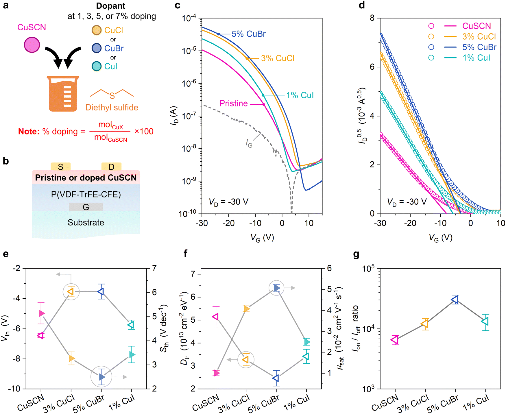 | ||
Fig. 1 (a) Schematic of the solution-based CuSCN doping process by CuX, where X = Cl, Br, or I. The solvent employed was diethyl sulfide (DES). The calculation for the % doping is also annotated. (b) Schematic structure of the bottom-gate top-contact (BG-TC) thin-film transistors (TFTs) employing CuSCN as the p-type channel. (c) Transfer characteristics (drain current IDvs. gate voltage VG) at a drain voltage VD = −30 V of TFTs based on pristine and doped CuSCN. Only forward sweeps are shown for clarity. (d) Plots of  vs. VG. (e)–(g) TFT device performance metrics: threshold voltage (Vth), subthreshold swing (Sth), trap state density (Dtr), saturation hole mobility (μsat), and on/off drain current ratio (Ion/Ioff). For (c)–(g), Only the best condition (achieving highest μsat) for each dopant is shown: 3% for CuCl, 5% for CuBr, and 1% for CuI. vs. VG. (e)–(g) TFT device performance metrics: threshold voltage (Vth), subthreshold swing (Sth), trap state density (Dtr), saturation hole mobility (μsat), and on/off drain current ratio (Ion/Ioff). For (c)–(g), Only the best condition (achieving highest μsat) for each dopant is shown: 3% for CuCl, 5% for CuBr, and 1% for CuI. | ||
2. TFT performance of CuX-doped CuSCN
TFTs were fabricated in the bottom-gate top-contact (BG-TC) architecture (Fig. 1b) featuring Al (40 nm) as the bottom gate electrode and poly(vinylidene fluoride-trifluoroethylene-chlorofluoroethylene) [P(VDF-TrFE-CFE), 500 nm, geometric capacitance 96 nF cm−2] as the gate dielectric. Pristine (undoped) and CuX-doped CuSCN layers (35 ± 3 nm) were deposited as the p-channel, and Au (25 nm) was employed as the top source/drain electrodes. As the high-k polymer dielectric required a long period of annealing (3 h at 80 °C, see details in the ESI†),7 the bottom-gate structure was employed to avoid the effects of extended heating that might volatilize the halide species.22,23 The top-contact was selected as it has been reported that the staggered device architecture can minimize the contact resistance due to charge injection.24 Devices were patterned with shadow masks to obtain channel lengths (L) between 30 and 100 μm and a channel width (W) of 1000 μm. The three dopants were tested at 1, 3, 5, and 7% doping [calculated from (molCuX/molCuSCN) × 100, see Table S1 in the ESI† for details]. The full results of representative transfer and output characteristics from all sample conditions are shown in Fig. S1–S4 (ESI†). For transfer characteristics, small hysteresis can be observed, similar to previous reports on CuSCN TFTs.6,18,25 Statistics of device parameters, including μsat, threshold voltage (Vth), Sth, and trap state density (Dtr) are shown in Fig. S5 and Table S2 (ESI†). Based on this data, the most optimal doping concentration that yielded the highest μsat for each dopant was 3% CuCl, 5% CuBr, and 1% CuI. These doping conditions are discussed in more detail below.
Fig. 1c displays the transfer characteristics of TFTs from the best condition for each dopant. All devices exhibited well-behaved p-channel character. Our reference pristine CuSCN TFTs displayed standard characteristics similar to previous reports.6,7,20,26 In CuX-doped devices, the drain current in the on-state (ID,on) was increased by 2 to 5 times whereas ID,off was not significantly affected. The plots between  and gate voltage (VG) (Fig. 1d) show a positive shift in Vth (from the x-intercept) and an increase in μsat (from the slope). Fig. 1e–g compare the Vth, Sth, Dtr, μsat, and Ion/Ioff of TFTs based on undoped CuSCN and the optimal condition of each dopant. Dtr was calculated from
 | (1) |
Notably, the observation that ID,off did not increase suggests that the p-doping effect was not significant in this case.15,27 In contrast, changes in other device parameters indicate that the addition of CuX led to VSCN defect healing,18,28,29 particularly evident from the concurrent positive shift in Vth and the reduction in Sth (Fig. 1e). Essentially, the shift in Vth (ΔVth) could be correlated to the interfacial trap filling (ΔNtr) (please see the ESI† for the calculation).27,30 The values of ΔVth and ΔNtr for the optimized TFTs are shown in Table S3 (ESI†). The average ΔVth of 3% CuCl and 5% CuBr was found to be similar, +2.92 V (requiring a smaller negative VG to turn the p-channel device on), corresponding to a decrease in the trap density of 1.75 × 1012 cm−2 (VSCN hole-trapping states filled by doping). For 1% CuI, ΔVth and ΔNtr were found to be +0.71 V and 4.3 × 1011 cm−2, respectively. Similarly, the subthreshold swing Sth is related to the overall trap state density Dtr;31,32 both of which were reduced upon CuX doping (Fig. 1f), reflecting the VSCN defect passivation effect (see Section 4 for discussion on VSCN defects and their passivation by halide ions). Ultimately, hole transport in CuSCN was significantly enhanced as evident from the higher μsat (Fig. 1g).
It is apparent that 5% CuBr yielded the best results overall, followed by 3% CuCl and 1% CuI. Comparing the average device parameters to those of pristine CuSCN, doping with 5% CuBr resulted in smaller Vth in terms of magnitude (from −6.45 to −3.53 V), reduced Sth (from 5.14 V to 2.50 V dec−1) and correspondingly lower Dtr (from 5.15 × 10¹³ to 2.47 × 1013 cm−2 eV−1), and enhanced μsat (from 0.01 to 0.05 cm2 V−1 s−1). Importantly, devices did not suffer from increased ID,off from the doping, and Ion/Ioff was in fact increased from ∼1 × 10⁴ to ∼3–4 × 10⁴ due to the enhancement in ID,on.
Next, the hole conduction mechanism was analyzed by fitting the VG dependence of field-effect hole mobility in the linear regime (μlin) with the power law equation:33
| μlin = K(VG − VP)γ | (2) |
 | ||
| Fig. 2 (a) Power law analysis of the relationship between linear mobility μlin and gate voltage VG. (b) Trap state density Dtrvs. power law exponent γ. (c) and (d) Gated transfer length method to find the contact resistance RcW from the plots of the total resistance RtW vs. channel length L for pristine and 5% CuBr-doped CuSCN devices, respectively. Note that the resistances are normalized by the channel width W. (e) VG dependence of RcW from (c) and (d). | ||
We also performed contact resistance (Rc) analysis to highlight the enhancement in device performance with CuX doping. The channel width-normalized RcW was determined by the gated transfer length method (gTLM,36 see details in the ESI†) as shown in Fig. 2c and d for pristine and 5% CuBr-doped CuSCN TFTs, respectively. As clearly evident, RcW was substantially decreased by approximately 1 order of magnitude to 1–2 × 10³ Ω cm upon doping with 5% CuBr (Fig. 2e). We infer that the suppression of Rc was also attributable to the defect healing effect. The reduction in charge trapping states within the semiconducting channel and at the semiconductor/dielectric interface mitigates the gate-field screening effect, leading to more effective charge injection and the apparent decrease in Rc as observed.37,38
To summarize the effects of CuX doping on TFT device performance, our simple method resulted in a significant improvement in hole transport properties in CuSCN by reducing the hole trapping states. Importantly, TFT devices did not suffer from Ion/Ioff reduction or subthreshold characteristics deterioration, typically associated with the p-doping effect.15,19,20 Instead, the performance enhancement can be attributed to VSCN defect passivation by CuX. The substitution of suitable anions to the VSCN sites (donor states, detrimental to hole transport)17 within CuSCN has been shown to recover the coordination environment and subsequently suppress defect concentration.18,26 Interestingly, CuCl and CuBr doping increased μsat by ∼4-fold and ∼5-fold, respectively, whereas CuI doping only improved μsat by ∼2.5 times. In addition, device performance gradually dropped when the concentration of CuI was higher than 1% (also agreeing with our previous report which found an optimal doping concentration with I2 to be 0.5 mol%).18 One of the reasons could be due to the size of the anions: 181 pm for Cl−, 196 pm for Br−, and 220 pm for I−, as compared to 213 pm for SCN−.39,40 The slightly smaller radii of Cl− and Br− could allow more favorable incorporation into CuSCN. However, the larger I− led to more structural distortion and impurity phase formation, especially at high doping concentrations, as shown in the following sections.
3. Effects of CuX doping on the optical, electronic, and structural properties of CuSCN
To understand the effects of CuX addition on the physical properties of CuSCN, samples of undoped CuSCN (as reference) and the optimal condition of each dopant: 3% CuCl, 5% CuBr, and 1% CuI, were further characterized. Ultraviolet-visible-near infrared (UV-vis-NIR) spectroscopy was employed to obtain the absorption spectra and determine the optical band gaps (Eg,opt) via Tauc plots (Fig. S6, ESI†). All doped samples displayed similar characteristics to those of reference CuSCN,18,20,26,41i.e., showing absorption peaks at 235 and 300 nm and having Eg,opt in the range of 3.78–3.81 eV. Clearly, CuX doping did not affect the optical transparency or create new electronic states. Next, photoelectron yield spectroscopy (PYS) and Kelvin probe (KP) measurements were performed to elucidate the electronic energy levels. The ionization potential or the valence band maximum (VBM) obtained from PYS (Fig. S7a, ESI†) and the Fermi level (EF) from KP allowed for the construction of a simplified energy band diagram as shown in Fig. S7b (ESI†). Note that the conduction band minimum (CBM) was estimated from VBM + Eg,opt. In general, the band diagram remained largely unaffected. While doping shifted EF slightly closer to the VBM, the effect was not dramatic, agreeing with the previous section that the p-doping effect was not significant.To study the morphology, CuSCN films engineered by CuX were investigated by atomic force microscopy (AFM). The films were deposited on the P(VDF-TrFE-CFE) dielectric layer in the same fashion as the TFT device structure. As shown in Fig. 3a–e, the reference CuSCN, 3% CuCl, and 1% CuI films showed the familiar character of rice-grained features but with some clustering,18,20 likely due to the interactions with the bottom dielectric layer.25 However, the film doped with 5% CuBr exhibited noticeably different morphology: flat surface with small grains. Fig. 3e and f display the histograms of the surface height distributions and root-mean-square roughness (σrms) obtained from the AFM images, respectively. While CuCl and CuI decreased σrms slightly, CuBr resulted in a dramatically smoother film with σrms reduced from 6.02 nm (reference CuSCN) to 1.31 nm (also similar to the value of the underlying dielectric layer). The improvement in film uniformity and ultrasmooth surface roughness should facilitate hole transport in CuBr-doped CuSCN when compared to other samples.26,31,42
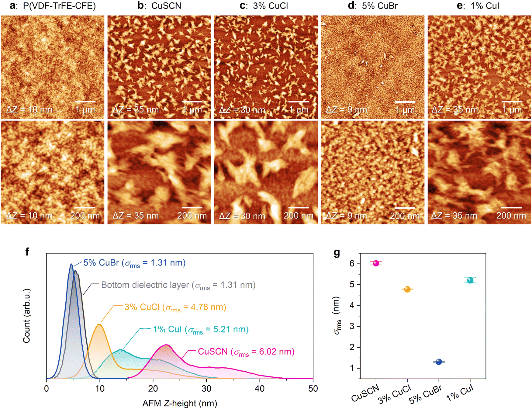 | ||
| Fig. 3 Surface heights from atomic force microscopy (AFM) of (a) P(VDF-TrFE-CFE) bottom dielectric layer, (b) CuSCN, (c) 3% CuCl, (d) 5% CuBr, and (e) 1% CuI. For (b) to (e), the films were deposited on top of the dielectric. Top row images: 5 μm × 5 μm. Bottom row images: 1 μm × 1 μm. (f) Surface height histograms and (g) root-mean-square roughness (σrms) of 5 μm × 5 μm images. | ||
X-ray diffraction (XRD) was then carried out to study the structural properties of CuX-doped CuSCN. In this case, the samples were prepared by drop-casting to increase the signal intensity. The pristine CuSCN prepared from DES-based solution expressed a distinct diffraction pattern identifiable as 3R β-CuSCN (ICSD 24372),43 similar to our previous results.18,20 As annotated in Fig. 4a, the prominent peaks at 2θ = 16.3°, 27.3°, 32.7°, 34.7°, 47.2°, and 50.0° can be assigned to diffractions from (0 0 6), (1 0 ![[2 with combining macron]](https://www.rsc.org/images/entities/char_0032_0304.gif) ), (0 0 12), (1 0
), (0 0 12), (1 0 ![[8 with combining macron]](https://www.rsc.org/images/entities/char_0038_0304.gif) ), (2
), (2 ![[1 with combining macron]](https://www.rsc.org/images/entities/char_0031_0304.gif) 0), and (2 6) planes, respectively. While Fig. 4a only shows the data of undoped CuSCN and the optimal condition of each dopant, the full results of all samples are included in Fig. S8a–c (ESI†). It is evident from the strong intensity of the (0 0 6) diffraction that the preferred orientation in all samples was with the c-axis of the CuSCN structure perpendicular to the plane of the substrate (‘vertical’ orientation, see Fig. S8d, ESI†). Interestingly, this preferential orientation was further intensified upon CuX doping as the diffractions from other planes diminished (Fig. 4b); the XRD patterns became strongly dominated by diffractions from (0 0 6) and (0 0 12) planes with some detectable signals from (1 0 ) planes. As diffraction from the latter signifies that the c-axis of β-CuSCN lies relatively flat with respect to the substrate (making a small angle to the substrate plane, ‘horizontal’ orientation, see Fig. S8e, ESI†), we then calculated the intensity ratios between (0 0 6) and (1 0 ) diffractions as a proxy to compare the preferential orientation. As shown in Fig. 4c, it becomes apparent that CuX doping preferentially led to the ‘vertical’ orientation. Since the large electronic dispersion in the valence band states (corresponding to low hole effective mass or high hole mobility) is strongly related to the plane of the Cu–S network in CuSCN,2,44 this preferred orientation could also contribute to the increase in μsat observed in CuX-doped TFT devices.
0), and (2 6) planes, respectively. While Fig. 4a only shows the data of undoped CuSCN and the optimal condition of each dopant, the full results of all samples are included in Fig. S8a–c (ESI†). It is evident from the strong intensity of the (0 0 6) diffraction that the preferred orientation in all samples was with the c-axis of the CuSCN structure perpendicular to the plane of the substrate (‘vertical’ orientation, see Fig. S8d, ESI†). Interestingly, this preferential orientation was further intensified upon CuX doping as the diffractions from other planes diminished (Fig. 4b); the XRD patterns became strongly dominated by diffractions from (0 0 6) and (0 0 12) planes with some detectable signals from (1 0 ) planes. As diffraction from the latter signifies that the c-axis of β-CuSCN lies relatively flat with respect to the substrate (making a small angle to the substrate plane, ‘horizontal’ orientation, see Fig. S8e, ESI†), we then calculated the intensity ratios between (0 0 6) and (1 0 ) diffractions as a proxy to compare the preferential orientation. As shown in Fig. 4c, it becomes apparent that CuX doping preferentially led to the ‘vertical’ orientation. Since the large electronic dispersion in the valence band states (corresponding to low hole effective mass or high hole mobility) is strongly related to the plane of the Cu–S network in CuSCN,2,44 this preferred orientation could also contribute to the increase in μsat observed in CuX-doped TFT devices.
 | ||
| Fig. 4 (a) X-ray diffraction (XRD) patterns of drop-cast samples. Simulated data of the 3R β-CuSCN phase are shown for diffraction plane identification. The broad feature around 20° is from the glass substrate. (b) Close-up of XRD patterns in the 2θ range of 25° to 55°. (c) Ratio of peak intensity between (0 0 6) and (1 0 ) diffractions. (d) Schematic of hole transport through the Cu–S network in CuSCN. | ||
When analyzing the (0 0 6) diffraction in more detail, we estimated the crystallite size using the Scherrer equation and found that the size slightly increased from 62 nm for undoped CuSCN to around 70 nm for the optimal doping conditions. We also noticed that the peaks of the CuCl- and CuI-doped samples remained largely similar to that of reference CuSCN whereas those of the CuBr-doped samples slightly shifted to lower diffraction angles (Fig. S8b, ESI†), signifying an expansion in the CuSCN lattice. The exact reason is still unknown. As the radius of Br− is in between that of Cl− and I−, the anion size may not be the only factor. We speculate that the specific interactions between the constituents (Cu+–Br− and SCN−–Br−) could play a role. However, this effect on the lattice may be related to the change in the morphology observed from the AFM images. The stress from the lattice expansion could prevent the grain growth, resulting in small grains and smooth morphology in CuBr-doped CuSCN films.
We also remark that for CuI doping, concentrations higher than 1% resulted in two extra XRD peaks at 19.9° and 25.0°, which can be identified as a segregated CuI impurity phase. The latter was confirmed by measuring a drop-cast sample of CuI (also processed with DES) which produced a similar XRD pattern (Fig. S8c, ESI†). The presence of the impurity phase could explain the limited TFT device performance in CuI-doped devices, especially with concentrations higher than 1%. While excess amount of dopants generally leads to reduced mobility due to impurity scattering,45,46 the case of CuI doping was exacerbated by the additional formation of the heterogeneous CuI phase.
4. Chemical states and defect healing effects
Chemical states of the samples were probed by X-ray photoelectron spectroscopy (XPS). The XPS survey scans confirmed the presence of Cu, S, N, C, and the relevant halide dopant in all samples (Fig. S9–S11, ESI†). Very small signals of O were detected, likely due to contamination from the atmospheric oxygen during sample transport. The high-resolution core-level spectra of Cu 2p, S 2p, N 1s and C 1s found the expected chemical states at typical binding energies (BE) similar to previous reports of CuSCN.26,47 In general, the Cu 2p core-level spectra showed that Cu was in the Cu(I) state with the intense Cu 2p3/2 peak found in the BE range of ∼932.7–932.9 eV. The satellite feature of Cu(II) was not detected.6,26 Moreover, Cu(I) species belonging to CuCl, CuBr, or CuI (with Cu 2p3/2 BE between 932.0 and 932.4 eV)48–50 were not found. We inferred that Cu atoms from the dopants were located at the Cu(I) sites of CuSCN (further corroborated by X-absorption experiments discussed below). This confirmed the chemical compatibility of Cu(I) halides as dopants in the CuSCN host. However, to determine whether these additional Cu(I) species also fill VCu sites or displace the original Cu(I) atoms of the host, further investigation is still needed. A system with a high concentration of VCu (i.e., CuSCN having high initial conductivity or high ID,off) should be synthesized first to allow for an objective analysis.51Next, the high-resolution S 2p and N 1s core-level spectra indicated the S–C![[triple bond, length as m-dash]](https://www.rsc.org/images/entities/char_e002.gif) N bonding state, associated with S 2p3/2 around ∼163.8 eV and N 1s ∼398.6–398.9 eV. For the latter state, a small and broad feature at a higher BE was observed in some samples. This has been assigned to N–H in previous reports.6,47 For C 1s, the spectra revealed two features: S–CN at 286.1–286.2 eV and adventitious carbon at 284.8 eV (used for referencing the XPS spectra). Overall, the chemical states of the CuSCN host remain largely unaffected by the addition of copper(I) halides at the concentrations studied in this work.
N bonding state, associated with S 2p3/2 around ∼163.8 eV and N 1s ∼398.6–398.9 eV. For the latter state, a small and broad feature at a higher BE was observed in some samples. This has been assigned to N–H in previous reports.6,47 For C 1s, the spectra revealed two features: S–CN at 286.1–286.2 eV and adventitious carbon at 284.8 eV (used for referencing the XPS spectra). Overall, the chemical states of the CuSCN host remain largely unaffected by the addition of copper(I) halides at the concentrations studied in this work.
XPS results also confirmed the existence of each dopant, and the high-resolution core-level spectra are shown in Fig. 5a–c for Cl 2p, Br 3d, and I 3d. At 1% doping, the signal intensity for Cl and Br was too low to be detected whereas the feature of I was easily detected due to its high sensitivity in XPS measurements.52,53 We note that the I 3d spectra overlapped with the Cu L2M23M45 (1P) Auger electron peak at BE ∼629 eV,52,54 which we carefully accounted for in the quantitative analysis of iodine. In general, the signal intensity of halides gradually increased with the increasing amount of added dopant. Fig. 5d shows the plots between the atomic percentage of the dopants found from XPS vs. the nominal doping concentration (converted to mol%) (see also Table S1, ESI†). The quantities found from XPS were lower than the amounts initially added in the solution, possibly limited by the thermodynamic equilibrium of the modified structure. Also, some halides may have been lost during film annealing due to their volatile nature.55,56
 | ||
| Fig. 5 X-ray photoelectron spectroscopy (XPS) high-resolution core-level scans of (a) Cl 2p, (b) Br 3d, and (c) I 3d in doped CuSCN samples. Solid circles indicate the experimental data points, shaded areas indicate the deconvoluted fitting components, colored lines indicate the sum of the fitting, and grey lines indicate the background. (d) Plots between the amount of dopants initially added in mol% vs. the amount found by XPS in at%. | ||
Furthermore, the local environment around Cu atom was characterized in detail by synchrotron-based X-ray absorption spectroscopy (XAS, details in the ESI†) with the full results shown in Fig. S12 (ESI†). Fig. 6a displays the X-ray absorption near edge structure (XANES) data of undoped CuSCN and the optimally doped condition for each CuX dopant. The rising edge at 8984 eV could be attributed to the 1s → 4p electronic transition of Cu+. The 1s → 3d transition of Cu2+ was not detected as no features of the pre-edge at energies below 8980 eV were observed, indicating that the oxidation of Cu+ to Cu2+ did not occur through the doping process.57,58 The overall XANES spectra were consistent with the pattern of 4-coordinate Cu+ (d10) previously reported in the literature.18,20,26,59 The results corroborate our XPS discussion that Cu existed in the Cu(I) state in all samples. Comparing the white line (the highest absorption peak at 8997 eV), samples doped with 3% CuCl and 5% CuBr exhibited noticeably higher intensities than that of undoped CuSCN, signifying improvement in the coordination number of Cu.60–62 A similar observation was previously reported and could be explained with the defect healing effect.18
 | ||
| Fig. 6 (a) X-ray absorption near-edge structures (XANES) and (b) extended X-ray absorption fine structures (EXAFS) in R-space at Cu K-edge of undoped CuSCN and the optimal concentration for each dopant. The radial distance (R) is shown without phase shift correction. | ||
Defect passivation could be further confirmed by the extended X-ray absorption fine structure (EXAFS) results shown in Fig. 6b (data in k-space are shown in Fig. S12, ESI†). The spectrum of CuSCN standard typically exhibits a dominant peak at 1.87 Å and another feature around ∼1.5 Å, attributed to the scattering paths of Cu–S and Cu–N bonding, respectively.18,20,63 For the undoped CuSCN sample, we observed that the overall environment of Cu atom became less well defined when compared to the standard. This evidence signifies the defective coordination environment around Cu in the reference sample prepared from dissolving CuSCN in DES. As reported in our previous work, DES can coordinate strongly to Cu(I),26 and the subsequent removal during annealing can lead to the formation of incomplete bonding, i.e., VSCN defects, around Cu.18 As VSCN are donor states, they are detrimental to the hole transport.17,18,64 With the optimal addition of CuX dopants, especially CuCl and CuBr, the EXAFS spectra displayed similar profiles to that of the CuSCN standard, indicating the remarkable recovery of the local structure around Cu atoms. Specifically, the voids associated with VSCN around Cu were effectively passivated. We previously reported a detailed study in which I− could fill in the defective VSCN site, restoring the Cu coordination environment.18 Based on similar XAS results in this work, we infer that Cl− and Br− could also passivate VSCN defects in CuSCN. As seen from the TFT results, the trap state density was reduced while hole mobility was significantly improved in CuCl- and CuBr-doped devices. We note that while CuI doping somewhat produced similar effects at 1% doping (as expected from I−), the samples mainly suffered from the formation of the impurity CuI phase at higher concentrations which greatly hindered hole transport.
5. Conclusions
We have shown that CuX dopants, with X = Cl, Br, or I, could significantly improve the performance of CuSCN p-channel TFT devices. The optimal concentrations were found to be: 3% CuCl, 5% CuBr, and 1% CuI. Specifically for CuBr doping, μsat was increased by ∼5 times up to 0.05 cm2 V−1 s−1. Importantly, the Ion/Ioff ratio was also increased to 3–4 × 10⁴ as ID,off did not increase upon the addition of CuX dopants, suggesting that there was minimal p-doping effect. The enhancement in the device performance was accompanied by a reduction in Dtr by about 2 times, from 5.2 × 10¹³ down to 2.5 × 1013 cm−2 eV−1. The latter could be explained with the defect healing effect. XAS results clearly showed that the defective coordination environment around Cu due to VSCN defects was effectively passivated by Cl− and Br−. While I− could also heal the defects, the CuI impurity phase easily formed, adversely affecting the hole transport. Our solution-based doping method reported herein employs common chemicals, CuCl and CuBr, which can be added directly to the standard CuSCN processing recipe. As CuSCN is now employed as a hole transport layer in a wide range of devices, this method can be easily applied to improve the performance or efficiency of various electronic and optoelectronic applications.Author contributions
Patipan Sukpoonprom: methodology, investigation, validation, formal analysis, data curation, visualization, and writing – original draft. Pinit Kidkhunthod: methodology, investigation, validation, and data curation (XAS). Chitsanucha Chattakoonpaisarn: investigation. Somlak Ittisanronnachai: methodology, investigation, and supervision. Taweesak Sudyoadsuk: methodology and supervision. Vinich Promarak: resources and funding acquisition. Pichaya Pattanasattayavong: conceptualization, funding acquisition, resources, project administration, supervision, visualization, and writing – review & editing.Data availability
The data supporting this article have been included as part of the ESI.†Conflicts of interest
There are no conflicts to declare.Acknowledgements
This research is funded by the National Research Council of Thailand (NRCT) under grant number N42A650255. This material is based upon work supported by the Air Force Office of Scientific Research under award number FA2386-22-1-4082. P. S. and P. P. acknowledge Vidyasirimedhi Institute of Science and Technology (VISTEC) for PhD scholarship and research funding and VISTEC's Frontier Research Center (FRC) for scientific instruments.References
- C. Wechwithayakhlung, D. M. Packwood, J. Chaopaknam, P. Worakajit, S. Ittisanronnachai, N. Chanlek, V. Promarak, K. Kongpatpanich, D. J. Harding and P. Pattanasattayavong, Tin(II) Thiocyanate Sn(SCN)2-a Wide Band Gap Coordination Polymer Semiconductor with a 2D Structure, J. Mater. Chem. C, 2019, 7(12), 3452–3462, 10.1039/c8tc06150e.
- P. Pattanasattayavong, D. M. Packwood and D. J. Harding, Structural Versatility and Electronic Structures of Copper(I) Thiocyanate (CuSCN)-Ligand Complexes, J. Mater. Chem. C, 2019, 7(41), 12907–12917, 10.1039/c9tc03198g.
- X. Huang, P. Sheng, Z. Tu, F. Zhang, J. Wang, H. Geng, Y. Zou, C. Di, Y. Yi, Y. Sun, W. Xu and D. Zhu, A Two-Dimensional π–d Conjugated Coordination Polymer with Extremely High Electrical Conductivity and Ambipolar Transport Behaviour, Nat. Commun., 2015, 6(1), 7408, DOI:10.1038/ncomms8408.
- Y. Li, X. Jiang, Z. Fu, Q. Huang, G.-E. Wang, W.-H. Deng, C. Wang, Z. Li, W. Yin, B. Chen and G. Xu, Coordination Assembly of 2D Ordered Organic Metal Chalcogenides with Widely Tunable Electronic Band Gaps, Nat. Commun., 2020, 11(1), 261, DOI:10.1038/s41467-019-14136-8.
- P. M. Crossland, C.-Y. Lien, L. O. de Jong, J. L. Spellberg, M. E. Czaikowski, L. Wang, A. S. Filatov, S. B. King and J. S. Anderson, Processable Coordination Polymer Inks for Highly Conductive and Robust Coatings, J. Am. Chem. Soc., 2024, 146(49), 33608–33615, DOI:10.1021/jacs.4c11178.
- N. Wijeyasinghe, A. Regoutz, F. Eisner, T. Du, L. Tsetseris, Y. H. Lin, H. Faber, P. Pattanasattayavong, J. Li, F. Yan, M. A. McLachlan, D. J. Payne, M. Heeney and T. D. Anthopoulos, Copper(I) Thiocyanate (CuSCN) Hole-Transport Layers Processed from Aqueous Precursor Solutions and Their Application in Thin-Film Transistors and Highly Efficient Organic and Organometal Halide Perovskite Solar Cells, Adv. Funct. Mater., 2017, 27(35), 1701818, DOI:10.1002/adfm.201701818.
- P. Pattanasattayavong, N. Yaacobi-Gross, K. Zhao, G. O. N. Ndjawa, J. Li, F. Yan, B. C. O’Regan, A. Amassian and T. D. Anthopoulos, Hole-Transporting Transistors and Circuits Based on the Transparent Inorganic Semiconductor Copper(I) Thiocyanate (CuSCN) Processed from Solution at Room Temperature, Adv. Mater., 2013, 25(10), 1504–1509, DOI:10.1002/adma.201202758.
- N. Arora, M. I. Dar, A. Hinderhofer, N. Pellet, F. Schreiber, S. M. Zakeeruddin and M. Grätzel, Perovskite Solar Cells with CuSCN Hole Extraction Layers Yield Stabilized Efficiencies Greater than 20%, Science, 2017, 358(6364), 768–771, DOI:10.1126/science.aam5655.
- Y. Chen, Y. Zheng, J. Wang, X. Zhao, G. Liu, Y. Lin, Y. Yang, L. Wang, Z. Tang, Y. Wang, Y. Fang, W. Zhang and X. Zhu, Ultranarrow-Bandgap Small-Molecule Acceptor Enables Sensitive SWIR Detection and Dynamic Upconversion Imaging, Sci. Adv., 2024, 10(23), eadm9631, DOI:10.1126/sciadv.adm9631.
- P. Pattanasattayavong, A. D. Mottram, F. Yan and T. D. Anthopoulos, Study of the Hole Transport Processes in Solution-Processed Layers of the Wide Bandgap Semiconductor Copper(I) Thiocyanate (CuSCN), Adv. Funct. Mater., 2015, 25(43), 6802–6813, DOI:10.1002/adfm.201502953.
- P. Pattanasattayavong, V. Promarak and T. D. Anthopoulos, Electronic Properties of Copper(I) Thiocyanate (CuSCN), Adv. Electron. Mater., 2017, 3(3), 1600378, DOI:10.1002/aelm.201600378.
- H. Faber, S. Das, Y.-H. Lin, N. Pliatsikas, K. Zhao, T. Kehagias, G. Dimitrakopulos, A. Amassian, P. A. Patsalas and T. D. Anthopoulos, Heterojunction Oxide Thin-Film Transistors with Unprecedented Electron Mobility Grown from Solution, Sci. Adv., 2017, 3(3), e1602640, DOI:10.1126/sciadv.1602640.
- J. W. Park, B. H. Kang and H. J. Kim, A Review of Low-Temperature Solution-Processed Metal Oxide Thin-Film Transistors for Flexible Electronics, Adv. Funct. Mater., 2020, 30(20), 1904632, DOI:10.1002/adfm.201904632.
- A. Charnas, Z. Zhang, Z. Lin, D. Zheng, J. Zhang, M. Si and P. D. Ye, Review-Extremely Thin Amorphous Indium Oxide Transistors, Adv. Mater., 2024, 36(9), 2304044, DOI:10.1002/adma.202304044.
- N. Wijeyasinghe, F. Eisner, L. Tsetseris, Y. H. Lin, A. Seitkhan, J. Li, F. Yan, O. Solomeshch, N. Tessler, P. Patsalas and T. D. Anthopoulos, p-Doping of Copper(I) Thiocyanate (CuSCN) Hole-Transport Layers for High-Performance Transistors and Organic Solar Cells, Adv. Funct. Mater., 2018, 28(31), 1802055, DOI:10.1002/adfm.201802055.
- J. E. Jaffe, T. C. Kaspar, T. C. Droubay, T. Varga, M. E. Bowden and G. J. Exarhos, Electronic and Defect Structures of CuSCN, J. Phys. Chem. C, 2010, 114(19), 9111–9117, DOI:10.1021/jp101586q.
- L. Tsetseris, Copper Thiocyanate: Polytypes, Defects, Impurities, and Surfaces, J. Phys.: Condens. Matter, 2016, 28(29), 295801, DOI:10.1088/0953-8984/28/29/295801.
- P. Worakajit, P. Kidkhunthod, T. Thanasarnsurapong, S. Waiprasoet, H. Nakajima, T. Sudyoadsuk, V. Promarak, A. Boonchun and P. Pattanasattayavong, Origin of Hole-Trapping States in Solution-Processed Copper(I) Thiocyanate and Defect-Healing by I2 Doping, Adv. Funct. Mater., 2023, 33(25), 2209504, DOI:10.1002/adfm.202209504.
- J. W. Liang, Y. Firdaus, R. Azmi, H. Faber, D. Kaltsas, C. H. Kang, M. I. Nugraha, E. Yengel, T. K. Ng, S. De Wolf, L. Tsetseris, B. S. Ooi and T. D. Anthopoulos, Cl2-Doped CuSCN Hole Transport Layer for Organic and Perovskite Solar Cells with Improved Stability, ACS Energy Lett., 2022, 7(9), 3139–3148, DOI:10.1021/acsenergylett.2c01545.
- S. Waiprasoet, P. Kidkhunthod, H. Nakajima, S. Ittisanronnachai, P. Prayongkul, C. Chattakoonpaisarn, J. Songkerdthong, P. Sukpoonprom, T. Sudyoadsuk, V. Promarak and P. Pattanasattayavong, Doping of Copper(I) Thiocyanate (CuSCN) with Metal Chlorides for p-Channel Thin-Film Transistors, ACS Appl. Electron. Mater., 2024, 6(9), 6837–6848, DOI:10.1021/acsaelm.4c01223.
- P. Lin, A. Loganathan, I. Raifuku, M. Li, Y. Chiu, S. Chang, A. Fakharuddin, C. Lin, T. Guo, L. Schmidt-Mende and P. Chen, Pseudo-Halide Perovskite Solar Cells, Adv. Energy Mater., 2021, 11(28), 2100818, DOI:10.1002/aenm.202100818.
- Z. Li, L. Wang, R. Liu, Y. Fan, H. Meng, Z. Shao, G. Cui and S. Pang, Spontaneous Interface Ion Exchange: Passivating Surface Defects of Perovskite Solar Cells with Enhanced Photovoltage, Adv. Energy Mater., 2019, 9(38), 1902142, DOI:10.1002/aenm.201902142.
- A. Liu, H. Zhu, W. T. Park, S. J. Kang, Y. Xu, M. G. Kim and Y. Y. Noh, Room-Temperature Solution-Synthesized p-Type Copper(I) Iodide Semiconductors for Transparent Thin-Film Transistors and Complementary Electronics, Adv. Mater., 2018, 30(34), 1802379, DOI:10.1002/adma.201802379.
- C. H. Kim, Y. Bonnassieux and G. Horowitz, Fundamental Benefits of the Staggered Geometry for Organic Field-Effect Transistors, IEEE Electron Device Lett., 2011, 32(9), 1302–1304, DOI:10.1109/LED.2011.2160249.
- S. Waiprasoet, S. Ittisanronnachai, P. Worakajit, T. Sudyoadsuk, V. Promarak and P. Pattanasattayavong, Engineering High-k Oxide/CuSCN Interface for p-Channel Thin-Film Transistors, ACS Appl. Electron. Mater., 2024, 6(5), 3510–3521, DOI:10.1021/acsaelm.4c00289.
- P. Worakajit, F. Hamada, D. Sahu, P. Kidkhunthod, T. Sudyoadsuk, V. Promarak, D. J. Harding, D. M. Packwood, A. Saeki and P. Pattanasattayavong, Elucidating the Coordination of Diethyl Sulfide Molecules in Copper(I) Thiocyanate (CuSCN) Thin Films and Improving Hole Transport by Antisolvent Treatment, Adv. Funct. Mater., 2020, 30(36), 2002355, DOI:10.1002/adfm.202002355.
- A. Liu, H. Zhu and Y. Y. Noh, Molecule Charge Transfer Doping for p-Channel Solution-Processed Copper Oxide Transistors, Adv. Funct. Mater., 2020, 30(24), 2002625, DOI:10.1002/adfm.202002625.
- H. Cho, M. Sritharan, Y. Ju, P. Pujar, R. Dutta, W. S. Jang, Y. M. Kim, S. Hong, Y. Yoon and S. Kim, Se-Vacancy Healing with Substitutional Oxygen in WSe2 for High-Mobility p-Type Field-Effect Transistors, ACS Nano, 2023, 17(12), 11279–11289, DOI:10.1021/acsnano.2c11567.
- W. L. Kalb, F. Meier, K. Mattenberger and B. Batlogg, Defect Healing at Room Temperature in Pentacene Thin Films and Improved Transistor Performance, Phys. Rev. B: Condens. Matter Mater. Phys., 2007, 76(18), 184112, DOI:10.1103/PhysRevB.76.184112.
- J. Zhu; B. Hou; L. Chen; Q. Zhu; L. Yang; X. Zhou; P. Zhang; X. Ma and Y. Hao Threshold Voltage Shift and Interface/Border Trapping Mechanism in Al2O3/AlGaN/GaN MOS-HEMTs. In IEEE International Reliability Physics Symposium Proceedings; IEEE, 2018, vol. 2018-March, p PWB.11-PWB.14 DOI:10.1109/IRPS.2018.8353704.
- A. F. Paterson, R. Li, A. Markina, L. Tsetseris, S. Macphee, H. Faber, A. H. Emwas, J. Panidi, H. Bristow, A. Wadsworth, D. Baran, D. Andrienko, M. Heeney, I. McCulloch and T. D. Anthopoulos, n-Doping Improves Charge Transport and Morphology in the Organic Non-Fullerene Acceptor O-IDTBR, J. Mater. Chem. C, 2021, 9(13), 4486–4495, 10.1039/d0tc05861k.
- Y. Meng, G. Liu, A. Liu, H. Song, Y. Hou, B. Shin and F. Shan, Low-Temperature Fabrication of High Performance Indium Oxide Thin Film Transistors, RSC Adv., 2015, 5(47), 37807–37813, 10.1039/c5ra04145g.
- S. Lee, K. Ghaffarzadeh, A. Nathan, J. Robertson, S. Jeon, C. Kim, I. H. Song and U. I. Chung, Trap-Limited and Percolation Conduction Mechanisms in Amorphous Oxide Semiconductor Thin Film Transistors, Appl. Phys. Lett., 2011, 98(20), 203508, DOI:10.1063/1.3589371.
- C. Caroli, M. Cyrot and P. G. De Gennes, Electronic Transport in Amorphous Silicon Films, Phys. Rev. Lett., 1970, 25(8), 509–511 CrossRef.
- A. Bhoolokam, M. Nag, S. Steudel, J. Genoe, G. Gelinck, A. Kadashchuk, G. Groeseneken and P. Heremans, Conduction Mechanism in Amorphous InGaZnO Thin Film Transistors, Jpn. J. Appl. Phys., 2016, 55(1), 014301, DOI:10.7567/JJAP.55.014301.
- M. Waldrip, O. D. Jurchescu, D. J. Gundlach and E. G. Bittle, Contact Resistance in Organic Field-Effect Transistors: Conquering the Barrier, Adv. Funct. Mater., 2020, 30(20), 1904576, DOI:10.1002/adfm.201904576.
- C. Liu, Y. Xu, Y. Li, W. Scheideler and T. Minari, Critical Impact of Gate Dielectric Interfaces on the Contact Resistance of High-Performance Organic Field-Effect Transistors, J. Phys. Chem. C, 2013, 117(23), 12337–12345, DOI:10.1021/jp4023844.
- A. F. Paterson, A. D. Mottram, H. Faber, M. R. Niazi, Z. Fei, M. Heeney and T. D. Anthopoulos, Impact of the Gate Dielectric on Contact Resistance in High-Mobility Organic Transistors, Adv. Electron. Mater., 2019, 5(5), 1800723, DOI:10.1002/aelm.201800723.
- R. D. Shannon, Revised Effective Ionic Radii and Systematic Studies of Interatomic Distances in Halides and Chalcogenides, Acta Crystallogr. Sect. A, 1976, 32(5), 751–767, DOI:10.1107/S0567739476001551.
- Y. Iwadate, K. Kawamura, K. Igarashi and J. Mochinaga, Effective Ionic Radii of NO2- and SCN- Estimated in Terms of the Böttcher Equation and the Lorentz-Lorenz Equation, J. Phys. Chem., 1982, 86(26), 5205–5208, DOI:10.1021/j100223a028.
- P. Worakajit, T. Sudyoadsuk, V. Promarak, A. Saeki and P. Pattanasattayavong, Antisolvent Treatment of Copper(I) Thiocyanate (CuSCN) Hole Transport Layer for Efficiency Improvements in Organic Solar Cells and Light-Emitting Diodes, J. Mater. Chem. C, 2021, 9(32), 10435–10442, 10.1039/d1tc02897a.
- A. Liu, S. Nie, G. Liu, H. Zhu, C. Zhu, B. Shin, E. Fortunato, R. Martins and F. Shan, In Situ One-Step Synthesis of p-Type Copper Oxide for Low-Temperature, Solution-Processed Thin-Film Transistors, J. Mater. Chem. C, 2017, 5(10), 2524–2530, 10.1039/c7tc00574a.
- D. L. Smith and V. I. Saunders, The Structure and Polytypism of the β Modification of Copper(I) Thiocyanate, Acta Crystallogr., Sect. B, 1981, 37(10), 1807–1812, DOI:10.1107/s0567740881007309.
- D. M. Packwood and P. Pattanasattayavong, Disorder-Robust Bands from Anisotropic Orbitals in a Coordination Polymer Semiconductor, J. Phys.: Condens. Matter, 2020, 32(27), 275701, DOI:10.1088/1361-648X/ab7d65.
- G. Hautier, A. Miglio, G. Ceder, G.-M. Rignanese and X. Gonze, Identification and Design Principles of Low Hole Effective Mass p-Type Transparent Conducting Oxides, Nat. Commun., 2013, 4(1), 2292, DOI:10.1038/ncomms3292.
- R. Mansfield, Impurity Scattering in Semiconductors, Proc. Phys. Soc., London, Sect. B, 1956, 69(1), 76–82, DOI:10.1088/0370-1301/69/1/310.
- B. Wang, S. Nam, S. Limbu, J. S. Kim, M. Riede and D. D. C. Bradley, Properties and Applications of Copper(I) Thiocyanate Hole-Transport Interlayers Processed from Different Solvents, Adv. Electron. Mater., 2022, 8(7), 2101253, DOI:10.1002/aelm.202101253.
- R. P. Vasquez, CuCl by XPS, Surf. Sci. Spectra, 1993, 2(2), 138–143, DOI:10.1116/1.1247732.
- R. P. Vasquez, CuBr by XPS, Surf. Sci. Spectra, 1993, 2(2), 144–148, DOI:10.1116/1.1247733.
- R. P. Vasquez, CuI by XPS, Surf. Sci. Spectra, 1993, 2(2), 149–154, DOI:10.1116/1.1247734.
- G. K. Padam, G. L. Malhotra and S. K. Gupta, Study of Intrinsic Defects in Vacuum/Air Annealed CuInSe2, Sol. Energy Mater., 1991, 22(4), 303–318, DOI:10.1016/0165-1633(91)90037-L.
- J. F. Moulder; W. F. Stickle; P. E. Sobol; K. D. Bomben and J. Chastain, Handbook of X-Ray Photoelectron Spectroscopy a Reference Book of Standard Spectra for Identification and Interpretation of XPS Data, PerkinElmer Corporation, 1992 Search PubMed.
- F. A. Stevie and C. L. Donley, Introduction to X-Ray Photoelectron Spectroscopy, J. Vac. Sci. Technol., A, 2020, 38(6), 063204, DOI:10.1116/6.0000412.
- A. C. Miller and G. W. Simmons, Copper by XPS, Surf. Sci. Spectra, 1993, 2(1), 55–60, DOI:10.1116/1.1247725.
- K. B. Lohmann, S. G. Motti, R. D. J. Oliver, A. J. Ramadan, H. C. Sansom, Q. Yuan, K. A. Elmestekawy, J. B. Patel, J. M. Ball, L. M. Herz, H. J. Snaith and M. B. Johnston, Solvent-Free Method for Defect Reduction and Improved Performance of p-i-n Vapor-Deposited Perovskite Solar Cells, ACS Energy Lett., 2022, 7(6), 1903–1911, DOI:10.1021/acsenergylett.2c00865.
- H. Yu, F. Wang, F. Xie, W. Li, J. Chen and N. Zhao, The Role of Chlorine in the Formation Process of “CH3NH3PbI3−xClx” Perovskite, Adv. Funct. Mater., 2014, 24(45), 7102–7108, DOI:10.1002/adfm.201401872.
- M. L. Baker, M. W. Mara, J. J. Yan, K. O. Hodgson, B. Hedman and E. I. Solomon, K- and L-Edge X-Ray Absorption Spectroscopy (XAS) and Resonant Inelastic X-Ray Scattering (RIXS) Determination of Differential Orbital Covalency (DOC) of Transition Metal Sites, Coord. Chem. Rev., 2017, 345, 182–208, DOI:10.1016/j.ccr.2017.02.004.
- L. S. Kau, D. J. Spira-Solomon, J. E. Penner-Hahn, K. O. Hodgson and E. I. Solomon, X-Ray Absorption Edge Determination of the Oxidation State and Coordination Number of Copper. Application to the Type 3 Site in Rhus Vernicifera Laccase and Its Reaction with Oxygen, J. Am. Chem. Soc., 1987, 109(21), 6433–6442, DOI:10.1021/ja00255a032.
- C. Wechwithayakhlung, S. Wannapaiboon, S. Na-Phattalung, P. Narabadeesuphakorn, S. Tanjindaprateep, S. Waiprasoet, T. Imyen, S. Horike and P. Pattanasattayavong, Mixed-Metal Cu-Zn Thiocyanate Coordination Polymers with Melting Behavior, Glass Transition, and Tunable Electronic Properties, Inorg. Chem., 2021, 60(21), 16149–16159, DOI:10.1021/acs.inorgchem.1c01813.
- S. A. Azzam, A. Boubnov, A. S. Hoffman, T. López-Ausens, N. Chiang, G. Canning, P. Sautet, S. R. Bare and D. A. Simonetti, Insights into Copper Sulfide Formation from Cu and S K Edge XAS and DFT Studies, Inorg. Chem., 2020, 59(20), 15276–15288, DOI:10.1021/acs.inorgchem.0c02232.
- A. A. Guda, S. A. Guda, A. Martini, A. N. Kravtsova, A. Algasov, A. Bugaev, S. P. Kubrin, L. V. Guda, P. Šot, J. A. van Bokhoven, C. Copéret and A. V. Soldatov, Understanding X-Ray Absorption Spectra by Means of Descriptors and Machine Learning Algorithms, npj Comput. Mater., 2021, 7(1), 203, DOI:10.1038/s41524-021-00664-9.
- C. Prestipino, L. Regli, J. G. Vitillo, F. Bonino, A. Damin, C. Lamberti, A. Zecchina, P. L. Solari, K. O. Kongshaug and S. Bordiga, Local Structure of Framework Cu(II) in HKUST-1 Metallorganic Framework: Spectroscopic Characterization upon Activation and Interaction with Adsorbates, Chem. Mater., 2006, 18(5), 1337–1346, DOI:10.1021/cm052191g.
- Z. Zhao, H. Yang, Y. Zhu, S. Luo and J. Ma, Interfacial N-Cu-S Coordination Mode of CuSCN/C3N4 with Enhanced Electrocatalytic Activity for Hydrogen Evolution, Nanoscale, 2019, 11(27), 12938–12945, 10.1039/c9nr02860a.
- W. Ji, G. Q. Yue, F. S. Ke, S. Wu, H. B. Zhao, L. Y. Chen, S. Y. Wang and Y. Jia, Electronic Structures and Optical Properties of CuSCN with Cu Vacancies, J. Korean Phys. Soc., 2012, 60(8), 1253–1257, DOI:10.3938/jkps.60.1253.
Footnote |
| † Electronic supplementary information (ESI) available. See DOI: https://doi.org/10.1039/d5tc00574d |
| This journal is © The Royal Society of Chemistry 2025 |