 Open Access Article
Donor–acceptor–acceptor (D–A–A) type 1,8-naphthalimides as non-fullerene small molecule acceptors for bulk heterojunction solar cells†
Prabhat
Gautam
a,
Rahul
Sharma
a,
Rajneesh
Misra
*a,
M. L.
Keshtov
b,
S. A.
Kuklin
b and
Ganesh D.
Sharma
*c
aDepartment of Chemistry, Indian Institute of Technology Indore, Indore 453552, India. E-mail: rajneeshmisra@iiti.ac.in
bInstitute of Organoelement Compounds of the Russian Academy of Sciences, Vavilova St., 28, 119991 Moscow, Russian Federation
cDepartment of Physics, LNM Institute of Information Technology, Jamdoli, Jaipur 302031, Rajasthan, India. E-mail: gdsharma273@gmail.com
First published on 11th November 2016
Abstract
Donor–acceptor–acceptor (D–A–A) type 1,8-naphthalimide based small molecules SM1 and SM2 functionalized with tetracyanobutadiene (TCBD) and dicyanoquino-dimethane (DCNQ) modules, showing strong absorption in the visible and near-infrared (NIR) region are reported. TCBD and DCNQ linked SM1 and SM2 exhibit multi-redox waves. The electrochemical and optical HOMO–LUMO gaps show similar trends. These SMs exhibit a broad absorption profile which is complementary to the D–A copolymer P donor and also possess an appropriate lowest unoccupied molecular orbital (LUMO) to serve as an acceptor with P with a LUMO level of −3.33 eV. The organic solar cells based on P:SM1 and P:SM2 exhibit a PCE of 4.94% and 6.11%, respectively. The higher value of the PCE for the SM2 based organic solar cells has been attributed to the broader absorption profile, more balanced charge transport and lower photon energy loss. The values of Voc of the organic solar cells for the SM1 acceptor (1.06 V and 1.02 V without and with solvent additive) are the highest values reported for devices based on non-fullerene acceptors to the best of our knowledge. The energy loss (Eloss) of 0.56 eV and 0.48 eV for SM1 and SM2 based devices, respectively is one of the smallest reported for BHJ organic solar cells.
Introduction
In most of the efficient organic solar cells, fullerene derivatives have been extensively used as acceptor materials along with conjugated polymers or small molecules as donors, because of their advantages of high electron mobility and affinity, isotropy of charge transport, and the ability to form favorable nanoscale networks with donor materials.1 However, fullerene derivatives have certain drawbacks such as, poor photostability in air, poor solar energy harvesting, high production cost and difficulty in tuning the optical properties over a wide range of energy.2Non-fullerene organic acceptors have been extensively used during the last couple of years due to their different structures, easier tunability of energy levels, good absorption and ease of synthesis.3 High power conversion efficiencies (PCEs) in the range of 11–12% have been reported so far for OSCs based on non-fullerene organic acceptors.4 In general, non-fullerene organic acceptors should have broad and strong absorptions in the visible region of the solar spectrum, suitable HOMO/LUMO energy levels, good solubility is common organic solvents and high electron mobility. To achieve the above requirements, conjugated push–pull structures are used to construct non-fullerene acceptors, which could reduce the optical bandgap, extend absorption in the whole visible region of solar spectrum, and tune the energy levels. Moreover, to design a molecular system which exhibits effective intermolecular interactions is to have a large, planar and extended π-core which enhances π-stacking and reduces steric interactions. The supramolecular assembly of perylene diimides (PDIs) and naphthalenediimides (NDIs) and other amide based conjugated molecules have been incorporated in molecular systems which provides a potential strategy to tune their optical and electrochemical properties. NDIs are fluorescent redox-active planar materials that have a relatively high electron affinity (comparable to fullerene).5 Bloking et al. have reported a di-phthalimide containing small molecule with benzothiadiazole as the core and used it as an acceptor along with P3HT as an electron donor for the fabrication of bulk heterojunction (BHJ) organic solar cells and achieved a PCE of 2.54%.6 Naphthalimide (NI) based n-type small molecules with high electron mobility and low lying LUMO energy levels are promising acceptor materials for wide bandgap polymer based solar cells. Kwon et al. synthesized a dicyanodistyrylbenzene-naphthalimide (DCS-NI) type molecular acceptor and used it as a promising non-fullerene acceptor with good electron accepting properties and compatibility with both a polymer (P3HT)7 and a small molecule donor (p-DTS(FBTTH2)2),8 exhibiting a PCE of 2.71% and 5.44%, respectively. Chatterjee introduced a strong electron withdrawing group (naphtha[1,2-c:5,6-c′]bis[1,2,5]thizdiazole) in the di-naphthalimide system and successfully decreased the bandgap to 1.73 eV. The OSC devices exhibited a PCE of 2.81% by blending this with P3HT.9 Bo et al. have developed a series of NI based non-fullerene acceptors with PCEs of 2–3% when blended with a wide band gap polymer.10
The electron deficient 1,8-naphthalimide (NI) unit exhibits high electron affinity and high charge carrier mobility, and acts as an acceptor unit.11 However the D–A systems based on NIs have a wide energy gap.12 The electronic and photonic properties of the D–A NIs can be tuned by substitution at the C-4 or C-5 position.13 Recently cross conjugation has been utilized as a facile methodology to design low HOMO–LUMO gap molecular systems.14,15 A variety of cross conjugated 1,1,4,4-tetracyanobutadienes (TCBD) and dicyanoquinodimethane (DCNQ) derivatives have been synthesized via the [2 + 2] cycloaddition–retroelectrocyclization reaction between donor substituted alkynes and tetracyanoethylene (TCNE) and tetracyanoquinodimethane (TCNQ).16–18 The substitution of –CN in the molecular backbone can increase the electron affinity and promote the formation of a crystallite architecture by secondary interaction and/or local dipole alignments that favour efficient charge transport and also broaden the absorption profile towards a longer wavelength region, where the power density of the solar spectrum is higher.19
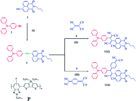
In this contribution, we wish to report triphenylamine-functionalized molecular systems of the type D–A1–A2. The triphenylamine substituted naphthalimide 3 was synthesized by the Pd-catalyzed Sonogashira cross-coupling reaction of compound 1 with 4-bromo-N,N-diphenylaniline 2. The reaction of NI 3 with TCNE and TCNQ resulted in SM1 and SM2 with strong intramolecular charge transfer. The introduction of TCNQ in the small molecule, i.e.SM2 showed a broader absorption profile extending up to 850 nm, attributed to the stronger electron withdrawing nature of TCNQ relative to TCNE. Both SM1 and SM2 possess relatively high lying LUMO energy levels than that of PC71BM, which would produce a high open circuit voltage, when used as an acceptor along with the conjugated D–A copolymer P (the chemical structure is shown in Scheme 1). After the optimization of the active layer (weight ratio and concentration of solvent additive), the devices based on P:SM1 and P:SM2 showed PCEs of 4.94% and 6.11% with a high Voc of 1.02 V and 0.92 V, respectively. Our results showed that these NI based small molecules can be potential acceptors for efficient organic solar cells using a copolymer and small molecule as donors.
Results and discussion
Synthesis of SM1 and SM2
The NI 1 was synthesized by the Pd-catalyzed Sonogashira coupling reaction of 4-bromo-1,8-naphthalimide with trimethylsilylacetylene followed by base catalyzed deprotection.20,21 The Sonogashira cross-coupling reactions of compound 1 with 4-bromotriphenylamine 2 resulted in compound 3 (Scheme 1).21,22 The naphthalimide based small molecules SM1 and SM2 were synthesized by the [2 + 2] cycloaddition–retroelectrocyclization reaction of compound 3 with tetracyanoethylene (TCNE) and 7,7,8,8-tetracyanoquinodimethane (TCNQ). The [2 + 2] cycloaddition–retroelectrocyclization reaction of NI 3 with one equivalent of TCNE in dichloromethane (DCM) resulted in SM1 in 65% yield (Scheme 1).23 The reactions of 7,7,8,8-tetracyanoquinodimethane (TCNQ) with NI 3 was carried out under microwave irradiation due to its sluggish nature. The reaction of NI 3 with one equivalent of TCNQ in 1,2-dichloroethane (DCE) at 100 °C under microwave irradiation for 48 h resulted in SM2 in 60% yield. SM1 and SM2 were purified by silica-gel column chromatography and well characterized by 1H, 13C NMR, and HRMS techniques (details are summarized in ESI†).Photophysical properties
The electronic absorption spectra of SM1 and SM2 were recorded in chloroform at room temperature (Fig. 1) and the data are listed in Table 1. These SMs exhibit two sets of absorption bands. The high energy absorption band between 330–414 nm corresponding to the π–π* transition was observed and the intramolecular charge transfer (ICT) transition was observed above 450 nm.11a,12 The incorporation of 1,1,4,4-tetracyanobutadiene (TCBD) and dicyanoquinodimethane (DCNQ) acceptor units result in a strong ICT band in SM1 and SM2. The small molecule SM2 exhibits a substantial bathochromic shift of the onset absorption wavelength when compared to SM1, which can be attributed to the presence of the strong electron withdrawing DCNQ unit.23 The absorption spectra of both SM1 and SM2 in a thin film show a redshift when compared to their absorption bands in solution due to the strong intermolecular interactions and effective solid state packing between the molecular backbones. The optical bandgaps estimated from the onsets of the absorption spectra in the thin films are 1.58 eV and 1.39 eV, for SM1 and SM2, respectively. Since both small molecules have the same D and A2, but different A1 (TCBD and DCNQ for SM1 and SM2, respectively), this difference may be attributed to the stronger withdrawing nature of DCNQ, relative to TCBD. The incorporation of the DCNQ acceptor unit results in a lower optical band gap for SM2 as compared to SM1, which indicates that the optical band gap is a function of acceptor strength in these triphenylamine-substituted napthalimides.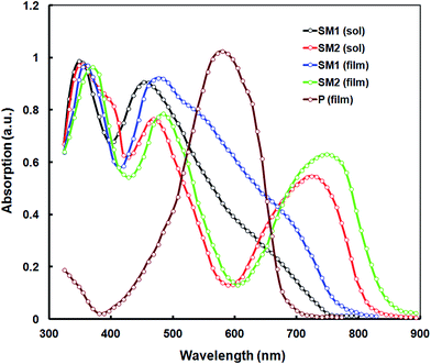 | ||
| Fig. 1 Normalized absorption spectra of SM1 and SM2 in dilute chloroform solution and thin film cast from chloroform and the absorption spectra of P is also shown. | ||
| Compound | λ abs (nm) | ε (M−1 cm−1) | E ox (V) | E red (V) | E elec (eV) | E op (eV) |
|---|---|---|---|---|---|---|
| a Absorbance measured in chloroform at 1 × 10⁻⁵ M concentration; λabs: maximum absorption wavelength; ε: extinction coefficient. b E ox and Ered are oxidation and reduction potentials. c E elec is the electrochemical band gap estimated by using the onset oxidation and reduction potential. d E op is the optical energy band gap estimated from the onset wavelength of the optical absorption in a dilute solution of chloroform (10−5), using the formula Eop = 1240/λonset where λonset is onset wavelength. | ||||||
| SM1 | 346 | 38![[thin space (1/6-em)]](https://www.rsc.org/images/entities/char_2009.gif) 360 360 |
1.14 | −0.32 | 1.44 | 1.64 |
| 451 | 34![[thin space (1/6-em)]](https://www.rsc.org/images/entities/char_2009.gif) 590 590 |
−0.76 | ||||
| −1.01 | ||||||
| SM2 | 353 | 34![[thin space (1/6-em)]](https://www.rsc.org/images/entities/char_2009.gif) 098 098 |
0.98 | −0.10 | 1.30 | 1.46 |
| 467 | 26![[thin space (1/6-em)]](https://www.rsc.org/images/entities/char_2009.gif) 994 994 |
−0.29 | ||||
| 722 | 18![[thin space (1/6-em)]](https://www.rsc.org/images/entities/char_2009.gif) 661 661 |
−1.10 | ||||
To maximize the light harvesting efficiency of BHJs, integrating electron donors and electron acceptors with complementary light absorption is advantageous. Therefore we have used the D–A conjugated copolymer P, which has an absorption peak around 578 nm (as shown in Fig. 1), which is blue-shifted compared to the SMs. The absorption spectra of the P donor and SM acceptors complement each other.
Electrochemical properties
The electrochemical properties of triphenylamine-substituted napthalimides SM1 and SM2 were explored by cyclic voltammetric (CV) analysis in chloroform solution using tetrabutylammonium hexafluorophosphate (Bu4NPF6) as the supporting electrolyte. The electrochemical data are listed in Table 1 and the cyclic voltammograms of SM1 and SM2 are shown in Fig. 2.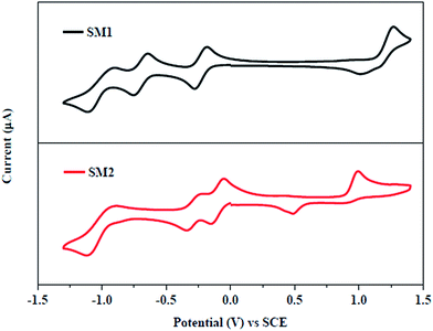 | ||
| Fig. 2 Cyclic voltammogram of SM1 and SM2 at 0.01 M concentration in 0.1 M Bu4NPF6 in chloroform recorded at a scan rate of 100 mV s−1. | ||
SM1 and SM2 exhibit multi-step redox waves corresponding to the reduction of naphthalimide, TCBD and DCNQ acceptor units, and the triphenylamine donor unit.11a,12b We have estimated the HOMO energy levels of SM1 and SM2 from EHOMO = −q(Eonsetoxid + 4.44) eV, where Eonsetoxid is the onset oxidation potential observed in cyclic voltammetry. The value of the HOMO energy levels for SM1 and SM2 are −5.56 eV and −5.44 eV, respectively. The LUMO energy levels of SM1 and SM2 were estimated according to ELUMO = EHOMO + Esolg and are −3.92 eV and −3.98 eV, respectively. The electrochemical studies show that the substitution of the DCNQ linkage in SM2 results in a lower Eelec as compared to TCBD linked SM1. The HOMO/LUMO energy levels of the conjugated copolymer P used as an electron acceptor are −5.30/−3.33 eV, therefore, the LUMO offsets between P and the acceptors SM1 and SM2 are 0.61 eV and 0.53 eV, respectively and are greater than the threshold value of 0.3 eV, indicating that these small molecules can be employed as electron acceptors for the BHJ PSCs along with P as the donor. Compared to the LUMO energy level of PC71BM (−4.1 eV), these SMs possessed high lying LUMO levels. When SM1 and SM2 were used as acceptor materials, a decreased offset values between the LUMO level of P and SMs reduced the energy loss, resulting in a higher Voc and PCE for the devices.24
Since the light absorption by the acceptors also contribute to the overall photocurrent generation of the devices, the hole transfer from the donor polymer P to acceptors needed to be considered. However, the HOMO offset is only 0.26 eV and 0.14 eV for SM1 and SM2, respectively, which is smaller than the widely used empirical threshold value of 0.3 eV. Although these systems have a small HOMO offset, these system showed efficient hole transfer from the acceptors (SM1 or SM2) to the conjugated polymer donor, which was confirmed by the IPCE values of the devices in the wavelength region beyond 650 nm where the light absorption by P is negligible,25 indicating that both the conjugated polymer P and small molecules contribute equally to photocurrent generation in the devices. In the literature, it has been reported that a small HOMO off set of 0.1 eV could be sufficient in separating the charge carriers in non-fullerene PSCs.26
Theoretical calculations
In order to explore the electronic structure of SM1 and SM2, density functional theory (DFT) calculations were performed at the B3LYP/6-31G** level.27 The contours of the HOMO and LUMO of SM1 and SM2 are shown in Fig. 3, the HOMO is localized on the electron donating triphenylamine unit. The incorporation of the TCBD and DCNQ acceptor unit in SM1 and SM2 results in delocalization of the LUMO over the TCBD, DCNQ and 1,8-naphthalimide acceptor units. The substitution of the strongly electron withdrawing DCNQ acceptor unit in SM2 results in a lower HOMO–LUMO gap and a red shift in the electronic absorption as compared to SM1. The values of the HOMO and LUMO energy levels are well in agreement with the estimated values from the cyclic voltammetry.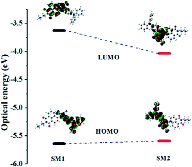 | ||
| Fig. 3 Correlation diagram showing the HOMO and LUMO wave functions and energies of SM1 and SM2 as determined at the B3LYP/6-31G** level (iso value = 0.02). | ||
Photovoltaic properties
To demonstrate the potential applications of SM1 and SM2 as acceptors in polymer solar cells, we blended these with the previously reported D–A copolymer P as a donor and fabricated BHJ PSCs with a device structure of ITO/PEDOT:PSS/P:SM1 or SM2/PFN/Al.28 The copolymer exhibited a D–A structure with dibromide 2-hexyl-4,7-dibromo-5-fluorobenzo-1,2,3-triazole and 4,4′-bis(2-ethylhexyl)-5,5′-bis(trimethyltin)-dithieno[3,2-b:2′,3′-d]silole acceptor and donor units respectively. The copolymer P exhibits a strong absorption band with an absorption maxima at 578 nm in the thin films, which is complementary to the absorption profiles of the SMs and suitable for the benefit of a higher light harvesting efficiency, when blended with these SMs as acceptors (the absorption spectra of the BHJ active layer cast from chloroform is shown in Fig. 4). In order to optimize the device performance, the effect of different D/A weight ratios and the concentration of the additive were investigated. The current–voltage characteristics of the optimized PSCs are shown in Fig. 5 (top) and corresponding data are summarized in Table 2. Without the use of an additive, the device based on P![[thin space (1/6-em)]](https://www.rsc.org/images/entities/char_2009.gif) :
:![[thin space (1/6-em)]](https://www.rsc.org/images/entities/char_2009.gif) SM1 (1
SM1 (1![[thin space (1/6-em)]](https://www.rsc.org/images/entities/char_2009.gif) :
:![[thin space (1/6-em)]](https://www.rsc.org/images/entities/char_2009.gif) 1) and P:SM2 showed overall PCEs of 2.34% (Jsc = 6.14 mA cm−2, Voc = 1.06 V and FF = 0.36) and 3.14% (Jsc = 8.02 mA cm−2, Voc = 0.98 V and FF = 0.40), respectively. After the addition of 3% DIO additive, the performance of the devices was significantly improved to 4.94% (Jsc = 9.15 mA cm−2, Voc = 1.02 V and FF = 0.54) and 6.11% (Jsc = 11.25 mA cm−2, Voc = 0.92 V and FF = 0.59) for SM1
1) and P:SM2 showed overall PCEs of 2.34% (Jsc = 6.14 mA cm−2, Voc = 1.06 V and FF = 0.36) and 3.14% (Jsc = 8.02 mA cm−2, Voc = 0.98 V and FF = 0.40), respectively. After the addition of 3% DIO additive, the performance of the devices was significantly improved to 4.94% (Jsc = 9.15 mA cm−2, Voc = 1.02 V and FF = 0.54) and 6.11% (Jsc = 11.25 mA cm−2, Voc = 0.92 V and FF = 0.59) for SM1![[thin space (1/6-em)]](https://www.rsc.org/images/entities/char_2009.gif) :P and SM2:P respectively.
:P and SM2:P respectively.
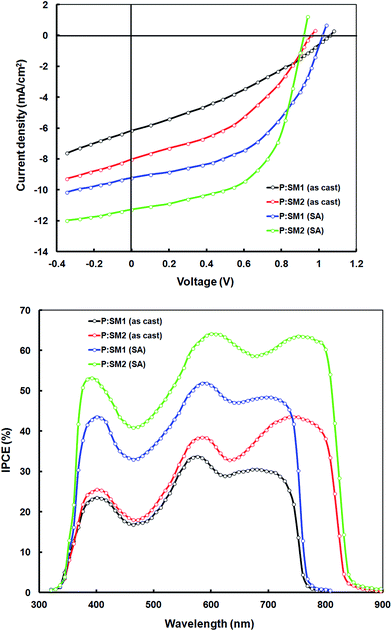 | ||
| Fig. 5 Current–voltage (J–V) characteristics under illumination (Top) and IPCE spectra of the devices based on P:SM1 and P:SM2 (Bottom). | ||
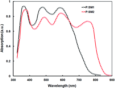
The PCEs of SM2 based devices is higher than that of their SM1 counterparts, primarily in terms of the enhanced Jsc and FF, which might be attributed to the broader absorption profile of SM2, which can facilitate the harvesting of more solar photons, enhanced electron mobility, optimal active layer morphology or combination of these factors. In order to explain these issues, we have measured the optical absorption spectra of the BHJ active layers (i.e. optimized P:SM1 and P:SM2) and these are shown in Fig. 4. It is noted that both the active layers showed absorption peaks corresponding to P and SMs, indicating that both the P donor and SM acceptors are contributing to exciton generation and thereby the Jsc of the devices. The absorption spectra of P:SM1 and P:SM2 is extended up to 770 nm and 850 nm, respectively, which can contribute to the enhanced Jsc.
We have measured the incident photon to current conversion efficiency (IPCE) response of the devices to verify the accuracy of the Jsc value obtained from the J–V characteristics and this is shown in Fig. 5 (bottom). The IPCE spectra of the devices closely resemble the absorption spectra of corresponding active layer (Fig. 4) demonstrating that both P and the SM acceptors contributed to photocurrent generation. Moreover, the IPCE values are significantly higher for the devices based on solvent additive processed active layers than the devices processed only from the chloroform solvent. The Jsc values estimated from the integration of the IPCE spectra are shown in Table 2, which are consistent with that obtained from the J–V characteristics of devices under illumination.
The Voc of the device based on the SM1 acceptor is higher than that of SM2, which is consistent with the reduced electron affinity (LUMO) of SM1 as compared to SM2, since the Voc of BHJ organic solar cells is directly related to the energy difference between the LUMO of the acceptor and the HOMO of the donor component employed in the active BHJ thin film. The value of Voc which is about 1.06 and 1.02 V for the SM1 acceptor is one of the highest values reported for devices based on non-fullerene acceptors.29 Moreover, the energy loss (Eloss) of 0.56 eV and 0.47 eV (Eloss = Eminopt − qVoc, where Eminopt is the smallest optical bandgap of either the donor or acceptor) for SM1 and SM2 based devices, respectively is one of the smallest reported for BHJ organic solar cells.30 Recently, Liu et al. reported a PCE of 9.7% for a non-fullerene organic solar cell with low energy loss.31
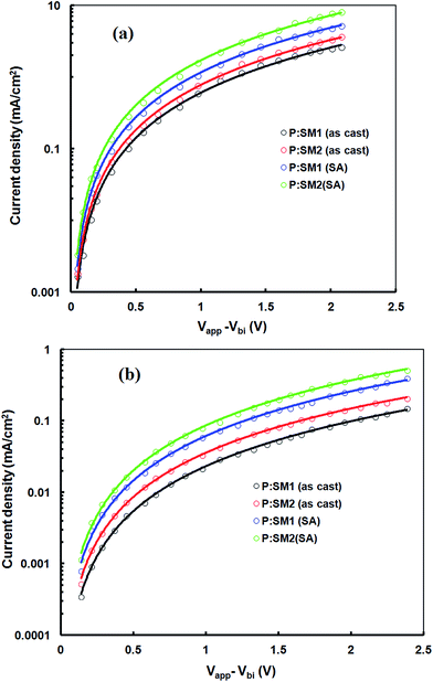
We have also examined the charge carrier mobility (hole and electron) of the active layers, based on the space charge limited current model, in order to get information about the charge transportation in the devices. The hole mobility (μh) and electron mobility (μe) were measured by hole only devices with a structure of ITO/PEDOT:PSS/P:SM1 or SM2/Au and electron only devices with a configuration of glass/Al/PEDOT:PSS/P:SM1 or SM2/Al. After acquiring the J–V characteristics in the dark (Fig. 6a and b for hole only and electron only devices, respectively), these curves were fitted by Mott–Gurney equation: J = 9ε0εrμV2/8L3. The μh/μe of the casted active layer P:SM1 and P:SM2 are 7.23 × 10⁻⁵/1.45 × 10−6 cm2 V−1 s−1 and 7.64 × 10⁻⁵/3.67 × 10−6 cm2 V−1 s−1, respectively. The low value of the electron mobilities for both active layers induces the mismatch between the μh and μe and causes the unbalanced charge transport in the active layer and leads to a lower Jsc and FF for the devices based on the casted active layers.32 After solvent additives, μh of P:SM1 and P:SM2 slightly increase up to 8.78 × 10⁻⁵ and 9.23 × 10⁻⁵ cm2 V−1 s−1, respectively, but μe for P:SM1 and P:SM2 increases significantly up to 3.45 × 10⁻⁵ and 5.78 × 10⁻⁵ cm2 V−1 s−1, respectively. The more pronounced increase in μe provides a more balanced charge transport in the active layer processed with solvent additives which leads to a higher Jsc and FF of the resulting OSCs.
In order to investigate the exciton dissociation and photocurrent generation in optimized devices based on SM1 and SM2 (only for DIO additive), the photocurrent density (Jph) is plotted as a function of effective voltage (Veff) for all the devices, as reported in the literature and shown in Fig. 7.33 The Jph is defined as Jph = JL − JD, where JL and JD are the current densities under illumination and in the dark, respectively, Veff is the given by Veff = V0 − Vappl, where V0 is the voltage at which Jph is zero and Vappl is the applied voltage. As shown in Fig. 7, Jph increase linearly with Veff in the low voltage region and reaches a plateau at high Veff. Therefore, we assume that at full saturation, all the excitons generated after photon absorption in the active layer are dissociated into free charge carriers and are subsequently collected by the respective electrodes. This allows us to estimate the maximum exciton generation and dissociation rate Gmax according to Jphsat = qGmaxL, where q is the elementary charge and L is the thickness of the active layer. The values of Gmax for SM1 and SM2 based devices are 8.0 × 1027 m−3 s−1 and 9.4 × 1027 m−3 s−1, respectively. The trend observed for Gmax for these devices is consistent with the enhancement of Jsc and IPCE spectra, indicating more exciton generation and dissociation in the SM2 based device. In addition, a charge collection probability (Pc) (Pc = Jsc/Jphsat) of 0.87 was obtained for the device based on SM2 and this is higher than that for the SM1 based device (0.76). The decreased bimolecular recombination and increased exciton dissociation contributed to the high Jsc and FF of the device.
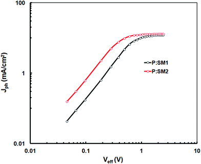 | ||
| Fig. 7 Variation of Jph with Veff for the devices based on P:SM1 and P:SM2 processed with SA (DIO/CF). | ||
In order to get information about the difference in the morphologies of the active layers based on P:SM1 and P:SM2 the TEM images of thin films processed with the solvent additive are shown in Fig. 8. The blended film of P:SM2 showed a much finer texture than P:SM1 which was processed under similar conditions. This morphology is beneficial for exciton dissociation, charge transfer between the SM2 acceptor to P (vice versa) and more effective charge transport in the P:SM2 active layer which results in increased Jsc and FF. However, the TEM image of the P:SM1 film showed a morphology with highly crystalline domains that hamper the exciton dissociation, resulting in relatively lower values of Jsc and FF.
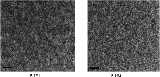 | ||
| Fig. 8 TEM images of optimized P:SM1 and P:SM2 thin films processed with solvent additives. Scale bar is 200 nm. | ||
Conclusion
In summary, donor–acceptor–acceptor (D–A–A) non-fullerene acceptors based on triphenylamine-substituted 1,8-naphthalimides derivatives SM1 and SM2 were designed and synthesized via [2 + 2] cycloaddition reaction of 3 with TCNE and TCNQ followed by subsequent ring-opening of the initially formed cyclobutene derivatives. The photophysical and electrochemical studies were performed to investigate the effect of acceptor strength modulation. The substitution of the acceptor DCNQ unit significantly lowers the HOMO–LUMO gap and results in a red shift of the absorption in the NIR region. The broad absorption, multi-step reduction waves and low HOMO–LUMO gap values make TCBD and DCNQ cross-conjugated NIs potential candidates for organic photovoltaics. The LUMO energy levels of these small molecules are about −3.94 and −3.98 eV and similar to that of PC71BM, which is used as an acceptor along with conjugated D–A copolymer P as a donor. After the optimization of the donor to acceptor weight ratio and solvent additive concentration, the organic solar cells based on P:SM1 and P:SM2 exhibit PCEs of 4.94% and 6.11%, respectively. The results obtained in this study will be useful for the design and synthesis of non-fullerene acceptor materials with a low HOMO–LUMO gap and for BHJ organic solar cells.Acknowledgements
The work was supported by DST (Project no. EMR/2014/001257), and CSIR (Project no. 01/(2795)/14/emr-II) Govt. of India, New Delhi. We are grateful to the Sophisticated Instrumentation Centre (SIC), IIT Indore. MLK and SA thankful to the Russian Foundation for Basic Research, grant number 14-03-92003 for financial support. GDS is thankful to the Director of The LNM Institute of Information Technology, Jaipur for financial support.References
- (a) J. B. You, L. T. Dou, K. Yoshimura, T. Kato, K. Ohya, T. Moriarty, K. Emery, C. C. Chen, J. Gao, G. Li and Y. Yang, Nat. Commun., 2013, 4, 1446 CrossRef PubMed; (b) J. D. Chen, C. Cui, Y. Q. Li, L. Zhou, Q. D. Ou, C. Li, Y. Li and J. X. Tang, Adv. Mater., 2015, 27, 1035 CrossRef CAS PubMed; (c) B. Kan, M. Li, Q. Zhang, F. Liu, X. Wan, Y. Wang, W. Ni, G. Long, X. Yang, H. Feng, Y. Zuo, M. Zhang, F. Huang, Y. Cao, T. P. Russell and Y. Chen, J. Am. Chem. Soc., 2015, 137, 3886 CrossRef CAS PubMed.
- (a) Y. Zhong, M. T. Trinh, R. Chen, W. Wang, P. P. Khlyabich, B. Kumar, Q. Xu, C. Y. Nam, M. Y. Sfeir, C. Black, M. L. Steigerwald, Y. L. Loo, S. Xiao, F. Ng, X. Y. Zhu and C. Nuckolls, J. Am. Chem. Soc., 2014, 136, 15215 CrossRef CAS PubMed; (b) H. Li, Y. J. Hwang, B. A. E. Courtright, F. N. Eberle, S. Subramaniyan and S. A. Jenekhe, Adv. Mater., 2015, 27, 3266 CrossRef CAS PubMed.
- (a) A. F. Eftaiha, J. P. Sun, I. G. Hill and G. C. Welch, J. Mater. Chem. A, 2014, 2, 1201 RSC; (b) C. Zhan, X. L. Zhang and J. Yao, RSC Adv., 2015, 5, 93002 RSC; (c) Y. Lin and X. Zhan, Adv. Energy Mater., 2015, 5, 1501063 CrossRef; (d) X. Guo, D. D. Tu and X. Liu, J. Energy Chem., 2015, 24, 675 CrossRef; (e) C. Zhan and J. Yao, Chem. Mater., 2016, 28, 1948 CrossRef CAS.
- (a) W. Zhao, Q. Qian, S. Zhang, S. Li, Q. Inganäs, F. Gao and J. Hou, Adv. Mater., 2016, 28, 4734 CrossRef CAS PubMed; (b) S. Li, L. Ye, W. Zhao, S. Zhang, S. Mukherjee, H. Ade and J. Hou, Adv. Mater., 2016, 28, 9423 CrossRef CAS PubMed.
- N. Sakai, J. Mareda, E. Vauthey and S. Matile, Chem. Commun., 2010, 46, 4225–4237 RSC.
- J. T. Bloking, X. Han, A. T. Higgs, J. P. Kastrop, L. Pandey, J. E. Norton, C. Risko, C. E. Chen, J. L. Brédas, M. D. McGehee and A. Sellinger, Chem. Mater., 2011, 23, 5484 CrossRef CAS.
- O. K. Kwon, J. H. Park, S. K. Park and S. Y. Park, Adv. Energy Mater., 2015, 5, 1400929 CrossRef.
- O. K. Kwon, J. H. Park, D. W. Kim, S. K. Park and S. Y. Park, Adv. Mater., 2015, 27, 1951 CrossRef CAS PubMed.
- S. Chatterjee, Y. Ie, M. Karakawa and Y. Aso, Adv. Funct. Mater., 2016, 26, 1161 CrossRef CAS.
- (a) J. Zhang, X. Zhang, G. Li, H. Xiao, W. Li, S. Xie, C. Li and Z. Bo, Chem. Commun., 2016, 52, 469 RSC; (b) J. Zhang, X. Zhang, H. Xiao, G. Li, Y. Liu, C. Li, H. Huang, X. Chen and Z. Bo, ACS Appl. Mater. Interfaces, 2016, 8, 5475 CrossRef CAS PubMed; (c) X. Zhang, J. Zhang, H. Lu, J. Wu, G. Li, C. Li, S. Li and Z. Bo, J. Mater. Chem. C, 2015, 3, 6979 RSC.
- (a) D. Gudeika, A. Michaleviciute, J. V. Grazulevicius, R. Lygaitis, S. Grigalevicius, V. Jankauskas, A. Miasojedovas, S. Jursenas and G. Sini, J. Phys. Chem. C, 2012, 116, 14811 CrossRef CAS; (b) F. Cacialli, R. H. Friend, C. M. Bouche, P. L. Barny, H. Facoetti, F. Soyer and P. J. Robin, J. Appl. Phys., 1998, 83, 2343 CrossRef CAS; (c) E. Martin and R. A. Weigand, Chem. Phys. Lett., 1998, 288, 52 CrossRef CAS; (d) C. Peebles, C. D. Wight and B. Iverson, J. Mater. Chem. C, 2015, 3, 12156 RSC; (e) A. R. Mallia, P. S. Salini and M. Hariharan, J. Am. Chem. Soc., 2015, 137, 15604 CrossRef CAS PubMed; (f) J. Zhang, H. Xiao, X. Zhang, Y. Wu, G. Li, C. Li, X. Chen, W. Ma and J. Bo, J. Mater. Chem. C, 2016, 4, 5656 RSC; (g) A. Saini and K. R. J. Thomas, RSC Adv., 2016, 6, 71638 RSC.
- D. Gudeika, J. V. Grazulevicius, D. Volyniuk, G. Juska, V. Jankauskas and G. Sini, J. Phys. Chem. C, 2015, 119, 28335 CAS.
- (a) J. L. Gu, E. Coronado, L. A. Martín, J. L. Montero, G. Fierro and J. M. García, J. Phys. Chem. A, 2007, 111, 9724 CrossRef PubMed; (b) J. P. Malval, S. Suzuki, F. M. Savary, X. Allonas, J. P. Fouassier, S. Takahara and T. Yamaoka, J. Phys. Chem. A, 2008, 112, 3879 CrossRef CAS PubMed; (c) D. Kolosov, V. Adamovich, P. Djurovich, M. E. Thompson and C. Adachi, J. Am. Chem. Soc., 2002, 124, 9945 CrossRef CAS PubMed; (d) O. K. Kwon, M. A. Uddin, J. H. Park, S. K. Park, T. L. Nguyen, H. Y. Woo and S. Y. Park, Adv. Mater., 2016, 28, 910 CrossRef CAS PubMed; (e) J. Zhang, X. Zhang, G. Li, H. Xiao, W. Li, S. Xie, C. Li and Z. Bo, Chem. Commun., 2016, 52, 469 RSC.
- W. C. W. Leu and C. S. Hartley, Org. Lett., 2013, 15, 3762 CrossRef CAS PubMed.
- (a) M. Gholami and R. R. Tykwinski, Chem. Rev., 2006, 106, 4997 CrossRef CAS PubMed; (b) A. J. Zucchero, P. L. McGrier and U. H. F. Bunz, Acc. Chem. Res., 2010, 43, 397 CrossRef CAS PubMed.
- (a) S. Kato and F. Diederich, Chem. Commun., 2010, 46, 1994 RSC; (b) M. Kivala, T. Stanoeva, T. Michinobu, B. Frank, G. Gescheidt and F. Diederich, Chem.–Eur. J., 2008, 14, 7638 CrossRef CAS PubMed; (c) T. Michinobu, I. Boudon, J. P. Gisselbrecht, P. Seiler, B. Frank, N. N. P. Moonen, M. Gross and F. Diederich, Chem.–Eur. J., 2006, 12, 1889 CrossRef CAS PubMed.
- T. Shoji, S. Ito, T. Okujimac and N. Moritad, Org. Biomol. Chem., 2012, 10, 8308 CAS.
- S. Niu, G. Ulrich, P. Retailleau and R. Ziessel, Org. Lett., 2011, 13, 4996 CrossRef CAS PubMed.
- T. Zhou, T. Jia, B. King, F. Li, M. Fahlman and Y. Wang, Adv. Energy Mater., 2011, 1, 431 CrossRef CAS.
- S. Ast, T. Fischer, H. Müller, W. Mickler, M. Schwichtenberg, K. Rurack and H. J. Holdt, Chem.–Eur. J., 2013, 19, 2990 CrossRef CAS PubMed.
- H. Gao, Y. Li, L. Wang, C. Ji, Y. Wang, W. Tian, X. Yang and L. Yin, Chem. Commun., 2014, 50, 10251 RSC.
- J. Li, F. Meng, H. Tian, J. Mi and W. Ji, Chem. Lett., 2005, 34, 922 CrossRef CAS.
- (a) R. Misra and P. Gautam, Org. Biomol. Chem., 2014, 12, 5448–5457 RSC; (b) P. Gautam, R. Misra, S. A. Siddiqui and G. D. Sharma, ACS Appl. Mater. Interfaces, 2015, 7, 10283 CrossRef CAS PubMed.
- J. Zhang, X. Zhang, G. Li, H. Xiao, W. Li, S. Xie, C. Li and Z. Bo, Chem. Commun., 2016, 52, 469 RSC.
- (a) H. Lin, S. Chen, Z. Li, J. Y. L. Lai, G. Yang, T. McAfcc, K. Jiang, Y. Li, Y. Liu, H. Hu, J. Zhao, W. Ma, H. Ade and H. Yan, Adv. Mater., 2015, 27, 7299 CrossRef CAS PubMed; (b) Y. Li, L. Zhong, F. Wu, Y. Yuan, H. Bin, Z. Jiang, Z. Zhang, Z. Zhang, Y. Lim and L. Liao, Energy Environ. Sci., 2016, 9, 3429 RSC.
- X. Gong, M. Tong, F. G. Brunetti, J. Seo, Y. Sun, D. Moses, F. Wudl and A. J. Heeger, Adv. Mater., 2011, 23, 2272 CrossRef CAS PubMed.
- M. J. Frisch; G. W. Trucks; H. B. Schlegel; G. E. Scuseria; M. A. Robb; J. R. Cheeseman; G. Scalmani; V. Barone; B. Mennucci; G. A. Petersson; H. Nakatsuji; M. Caricato; X. Li; H. P. Hratchian; A. F. Izmaylov; J. Bloino; G. Zheng; J. L. Sonnenberg; M. Hada; M. Ehara; K. Toyota; R. Fukuda; J. Hasegawa; M. Ishida; T. Nakajima; Y. Honda; O. Kitao; H. Nakai; T. Vreven; J. A. Montgomery Jr; J. E. Peralta; F. Ogliaro; M. Bearpark; J. J. Heyd; E. Brothers; K. N. Kudin; V. N. Staroverov; R. Kobayashi; J. Normand; K. Raghavachari; A. Rendell; J. C. Burant; S. S. Iyengar; J. Tomasi; M. Cossi; N. Rega; N. J. Millam; M. Klene; J. E. Knox; J. B. Cross; V. Bakken; C. Adamo; J. Jaramillo; R. Gomperts; R. E. Stratmann; O. Yazyev; A. J. Austin; R. Cammi; C. Pomelli; J. W. Ochterski; R. L. Martin; K. Morokuma; V. G. Zakrzewski; G. A. Voth; P. Salvador; J. J. Dannenberg; S. Dapprich; A. D. Daniels; O. Farkas; J. B. Foresman; J. V. Ortiz; J. Cioslowski and D. J. Fox, Gaussian 09, revision A.02, Gaussian, Inc., Wallingford, CT, 2009 Search PubMed.
- M. L. Keshtov, A. R. Khokhlov, S. A. Kuklin, I. E. Ostapov, A. Y. Nikolaev, I. O. Konstantinov, A. Sharma, E. N. Koukaras and G. D. Sharma, Polym. Chem., 2016, 7, 5849 RSC.
- (a) T. Kim, J. H. Kim, T. E. Kang, C. Lee, H. Kang, M. Shin, C. Wang, B. Ma, U. Jeong, T. S. Kim and B. J. Kim, Nat. Commun., 2015, 6, 8547 CrossRef CAS PubMed; (b) S. Li, H. Zhang, W. Zhao, L. Ye, H. Yao, B. Yang, S. Zhang and J. Hou, Adv. Energy Mater., 2016, 6, 1501991 CrossRef; (c) L. Gao, Z. G. Zhang, L. Xue, J. Min, J. Zhang, Z. Wei and Y. Li, Adv. Mater., 2016, 28, 1884 CrossRef CAS PubMed.
- (a) W. Li, K. H. Hendriks, A. Furlan, M. M. Wienk and R. A. J. Janssen, J. Am. Chem. Soc., 2015, 137, 2231 CrossRef CAS PubMed; (b) K. Kawashima, Y. Tamai, H. Ohkita, I. Osaka and K. Takimiya, High-efficiency polymer solar cells with small photon energy loss, Nat. Commun., 2015, 6, 10085 CrossRef CAS PubMed.
- J. Liu, S. Chen, D. Qian, B. Gautam, G. Yang, J. Zhao, J. Bergqvist, F. Zhang, W. Ma, H. Ade, O. Inganäs, K. Gundogdu, F. Gao and H. Yan, Nat. Energy, 2016, 1, 16089 CrossRef.
- D. Gupta, S. Mukhopadhyay and K. Narayan, Sol. Energy Mater. Sol. Cells, 2010, 94, 1309 CrossRef CAS.
- (a) C. M. Proctor, C. Kim, D. Neher and T. Q. Nguyen, Adv. Funct. Mater., 2013, 23, 3584 CrossRef CAS; (b) P. W. M. Blom, V. D. Mihailetchi, L. J. A. Koster and D. E. Markov, Adv. Mater., 2007, 19, 1551 CrossRef CAS; (c) V. D. Mihailetchi, H. X. Xie, B. de Boer, L. J. A. Koster and P. W. M. Blom, Adv. Funct. Mater., 2006, 16, 699 CrossRef CAS.
Footnote |
| † Electronic supplementary information (ESI) available: Copies of 1H, 13C NMR and HRMS spectra of new compounds. The DFT calculation data of SM1 and SM2. See DOI: 10.1039/c6sc04461a |
| This journal is © The Royal Society of Chemistry 2017 |

