
Semiconductor-based surface enhanced Raman scattering (SERS): from active materials to performance improvement
Xuejiao
Wang
 a,
Erjin
Zhang
*b,
Huimin
Shi
c,
Yufeng
Tao
a and
Xudong
Ren
*a
a,
Erjin
Zhang
*b,
Huimin
Shi
c,
Yufeng
Tao
a and
Xudong
Ren
*a
aInstitute of Micro-Nano Optoelectronics and Terahertz Technology, School of Mechanical Engineering, Jiangsu University, Zhenjiang 212013, People's Republic of China. E-mail: zhej@ujs.edu.cn; renxd@ujs.edu.cn
bInstitute for Energy Research, Jiangsu University, Zhenjiang 212013, People's Republic of China
cCollege of Physics and Electronic Engineering, Northwest Normal University, Lanzhou 730070, People's Republic of China
First published on 24th February 2022
Abstract
Surface enhanced Raman scattering (SERS) is a powerful spectral analysis technique and has exhibited remarkable application prospects in various fields. The design and fabrication of high-performance SERS substrates is key to promoting the development of SERS technology. Apart from noble metal substrates, non-metal substrates based on semiconductor materials have received increasing attention in recent years owing to their unique physical, chemical, and optical properties. However, compared with noble metal substrates, most semiconductor substrates show weak Raman enhancement ability. Therefore, exploring effective strategies to improve the SERS sensitivity is an urgent task. Numerous reviews have outlined the research progress of semiconductor SERS substrates, which mainly focused on summarizing the material category of semiconductor substrates. However, reviews that systematically summarize the strategies for improving the SERS performance of semiconductor substrates are lacking. In this review, we comprehensively discuss the research on semiconductor SERS from the aspects of mechanism, materials, and modification. Firstly, the Raman enhancement mechanism of semiconductor substrates and the SERS-active materials are discussed. Then, we summarize several effective approaches to boost the SERS performance of semiconductor substrates. In conclusion, we propose some prospects for this field.
 Xuejiao Wang | Xuejiao Wang received her Ph.D. from the College of Computer Science and Electronic Engineering, Hunan University in 2020. She joined Jiangsu University, China, in 2020. Currently, she is an assistant professor at the Institute of Micro-Nano Optoelectronics and Terahertz Technology, Jiangsu University, China. Her research interests focus on the fabrication and application of highly sensitive surface-enhanced Raman spectroscopy (SERS) substrates. |
 Erjin Zhang | Erjin Zhang received his Ph.D. from the School of Physics and Electronics, Hunan University in 2020. He joined Jiangsu University, China, in 2020. Currently, he is an assistant professor at the Institute for Energy Research, Jiangsu University, China. His current research direction is the design, synthesis, and application of functional materials in energy storage and conversion, and in situ Raman analysis of electrochemical reaction mechanisms. |
 Huimin Shi | Huimin Shi received his Ph.D. in Physics from Hunan University in 2018. Currently, he is an assistant professor at the School of Mechanical and Electrical Engineering, Guangzhou University, China. His research interests include the synthesis of nanomaterials, micro/nanomanufacturing and their relevant applications. |
 Yufeng Tao | Yufeng Tao received his Ph.D. from Nanjing Normal University in 2017. He completed his postdoctoral work at Huazhong University of Science and Technology in 2020. Currently, he is an assistant professor at the Institute of Micro-Nano Optoelectronics and Terahertz Technology, Jiangsu University, China. His research is focused on micro/nano optoelectronic devices and nanosensors. |
 Xudong Ren | Xudong Ren received his Ph.D. from Jiangsu University in 2009. He is currently a full professor at the School of Mechanical Engineering, Jiangsu University, China. His current research is concerned with laser advanced manufacturing and micro/nano optoelectronic devices. |
1 Introduction
Surface-enhanced Raman scattering (SERS) was first discovered by Fleischmann et al. in 1974 on the rough surface of a silver electrode.1 As a powerful spectroscopic technique, SERS achieves ultratrace detection by amplifying the Raman signal of molecules and possesses the advantages of high sensitivity, fingerprint specificity, and non-destructive detection. SERS has been widely used in various fields such as chemical and biological analysis,2,3 medical diagnosis,4,5 environmental analysis,6,7 food safety,8,9 and artwork restoration.10 At present, the widely accepted SERS enhancement mechanism includes the electromagnetic enhancement mechanism (EM) and the chemical enhancement mechanism (CM). The EM means that the strong electromagnetic field generated by the localized surface plasmon resonance (LSPR) of metal nanostructures can realize the Raman signal enhancement. The CM is relatively complex, mainly based on the charge transfer between the SERS substrate and the molecule adsorbed on its surface to achieve the Raman signal enhancement.11The SERS substrate is the core of SERS technology, and has extended from noble metals (Au, Ag, and Cu) and transition metals to semiconductor materials.12,13 In fact, the noble metal SERS substrate has always been dominant because it possesses an extremely high SERS enhancement factor (EF) (1010–1012) to achieve ultrasensitive and even single-molecule-level detection. However, there are some inevitable disadvantages for noble metal SERS substrates, such as poor stability, easy oxidation, high cost, poor reproducibility and biocompatibility, and lack of selective recognition ability for probe molecules.14 In addition, the strong photothermal effect at “hot spots” may cause significant damage to living cells.15 Semiconductor SERS substrates have been extensively studied in recent years.16Fig. 1a indicates that the publications related to semiconductor SERS have increased in recent years. Compared to noble metal SERS substrates, semiconductor substrates show better chemical stability, rich variety, and low price.16,17 Some semiconductor materials have excellent photocatalytic degradation ability, so the SERS substrate can be reused to improve the reproducibility of the SERS signal.18,19 Moreover, semiconductor substrates have better biocompatibility, exhibiting great application potential in life sciences. The selective Raman enhancement property enables semiconductor SERS substrates to recognize and detect target molecules in a complex environment.20 Significantly, the physical and chemical properties of semiconductor substrates such as exciton Bohr radius, band structure, and carrier concentration are easy to regulate.21 The above advantages can compensate for the bottleneck of noble metal SERS substrates. However, the EF of semiconductor substrates is generally low (10–102), hindering their practical applications.22 Therefore, developing novel SERS-active semiconductor materials and further improving the SERS performance of semiconductor substrates by adjusting their morphology, size, surface state, crystalline state, etc. is significant.
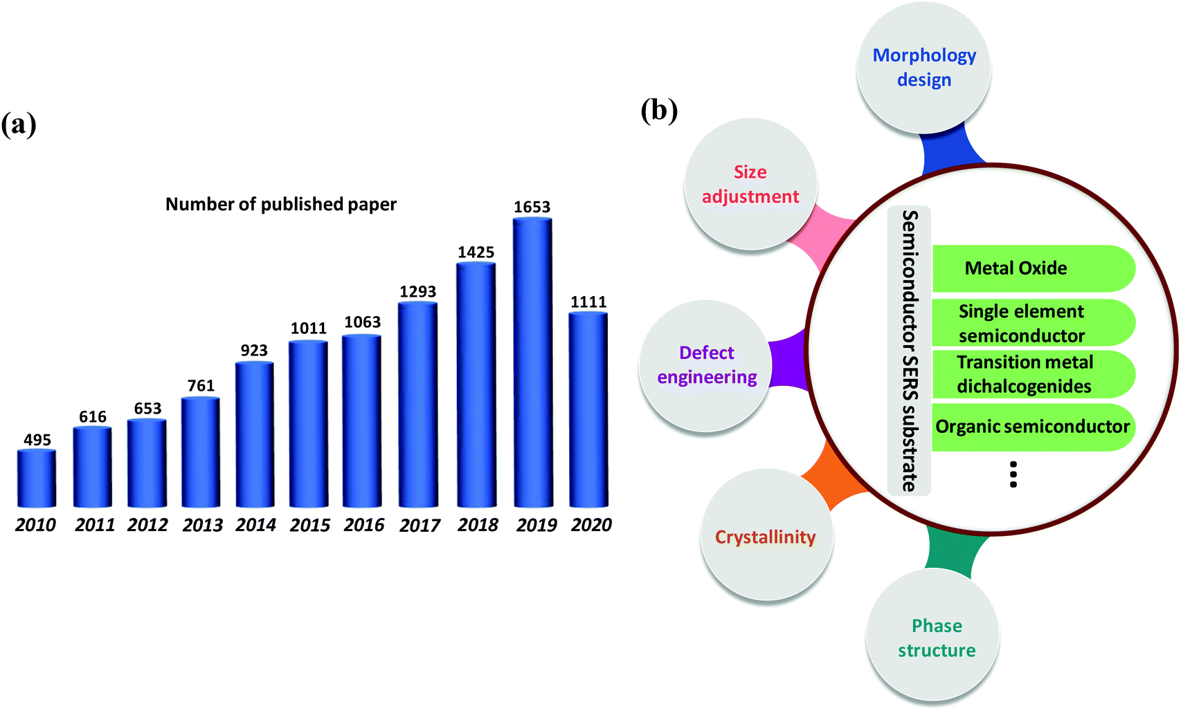 | ||
| Fig. 1 (a) Published papers related to semiconductor SERS in recent years (the data comes from Web of Science by searching the key word “semiconductor enhance Raman”). (b) Overview of this review. | ||
In this review, we focus on providing an overview of the strategies for enhancing the SERS performance of semiconductor substrates. We start with a brief introduction to several main types of semiconductor SERS substrates, including metal oxides, single element semiconductors, transition metal dichalcogenides, and organic semiconductors. As a guideline for semiconductor substrate design, the enhancement mechanism of semiconductor SERS substrates is also discussed. Next, as the core part of this review, we discuss various effective strategies for enhancing the SERS performance of semiconductor substrates such as adjusting the morphology, size, defect state, crystallinity, and phase structure. We mainly focus on the fabrication methods of these substrates and the working principle behind the enhanced SERS performance. Finally, we summarize the current development and challenges of semiconductor SERS substrates, and further highlight the prospects of semiconductor substrates from the aspect of design, fabrication and mechanism. Fig. 1b shows the overview of this mini-review.
2 A brief introduction to semiconductor SERS substrates
2.1 Enhancement mechanism of semiconductor SERS substrates
The free electrons in noble metals are prone to generate the LSPR effect under incident light excitation, so the enhancement mechanism of noble metal SERS substrates mainly originates from electromagnetic enhancement. In contrast, semiconductor substrates show a relatively complex mechanism. According to existing research results, the enhancement mechanism of semiconductor SERS substrates includes both EM and CM13 (Fig. 2).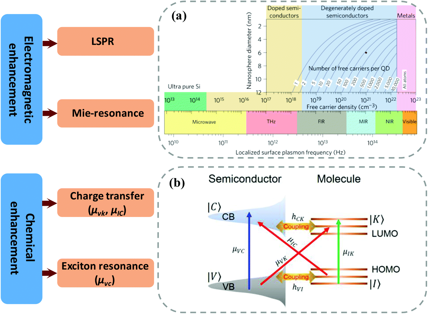 | ||
| Fig. 2 Raman enhancement mechanism of semiconductor substrates. (a) The regulation of localized surface plasmon frequency by doping. Reproduced with permission from ref. 24 (Copyright © 2011, Nature Publishing Group). (b) The charge transfer process in a semiconductor–molecule system. Reproduced with permission from ref. 29 (Copyright © 2019, American Chemical Society). | ||
2.2 Enhancement factor calculation
The EF is an important parameter for SERS performance evaluation. The definition of the EF is highly diverse including the single molecule enhancement factor, the SERS-active substrate enhancement factor, and the analytical enhancement factor. The SERS-active substrate enhancement factor is the most commonly used method to evaluate SERS performance and is defined as follows:where ISERS is the SERS intensity, IRaman is the classical Raman intensity obtained without the SERS substrate, and NSERS and NRaman stand for the number of molecules from the SERS substrate and classical Raman under laser illumination, respectively.
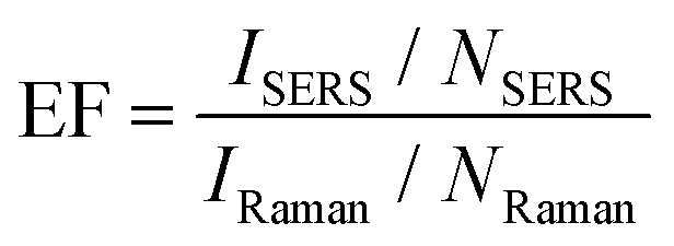
One of the difficulties in calculating the EF lies in the precise determination of NSERS because it is a tricky business to accurately obtain the surface coverage of target molecules and the surface area of SERS substrate.36 It should be noted that the accurate calculation of the EF requires that each parameter (ISERS, IRaman, NSERS, NRaman) be measured accurately. However, in actual calculation, some parameters are difficult to obtain accurately, and reasonable assumptions are required. There may be large differences in the EF obtained by different research groups. Therefore, more reliable methods need to be explored to evaluate SERS performance.
2.3 Semiconductor SERS substrates
Since the first observation of the SERS effect on the semiconductors NiO and TiO2 surface in 1982 by Yamada et al.,37,38 the species of semiconductor SERS substrates have become more abundant. More and more researchers are working on developing novel semiconductor SERS-active materials and further improving their SERS performance. In this part, we summarize several well-developed types of semiconductor SERS substrates in recent years, including metal oxides, single element semiconductors, transition metal dichalcogenides, and organic semiconductors.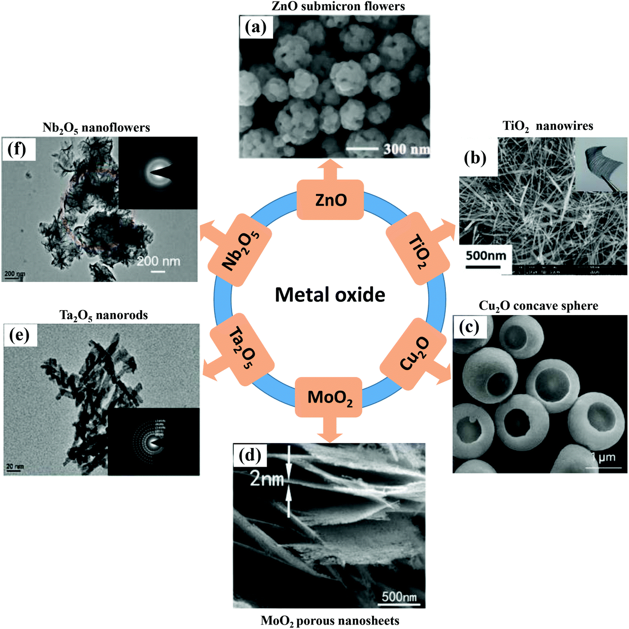 | ||
| Fig. 3 (a) SEM image of ZnO submicron flowers. Reproduced with permission from ref. 45 (Copyright © 2021 Elsevier B.V. All rights reserved). (b) SEM image of TiO2 nanowires. Reproduced with permission from ref. 46 (Copyright © 2018, American Chemical Society). (c) SEM image of Cu2O concave sphere. Reproduced with permission from ref. 47 (Copyright © 2018 WILEY-VCH Verlag GmbH & Co. KGaA, Weinheim). (d) SEM image of MoO2 monocrystalline ultrathin porous nanosheets. Reproduced with permission from ref. 48 (Copyright © 2019, Royal Society of Chemistry). (e) and (f) TEM image of Ta2O5 nanorods and Nb2O5 nanoflowers, insets are the corresponding selected area electron diffraction patterns. Reproduced with permission from ref. 49 and 50 (Copyright © 2019 The Authors. Published by WILEY-VCH Verlag GmbH & Co. KGaA, Weinheim; Copyright © 2020 The Authors. Published by Elsevier Ltd). | ||
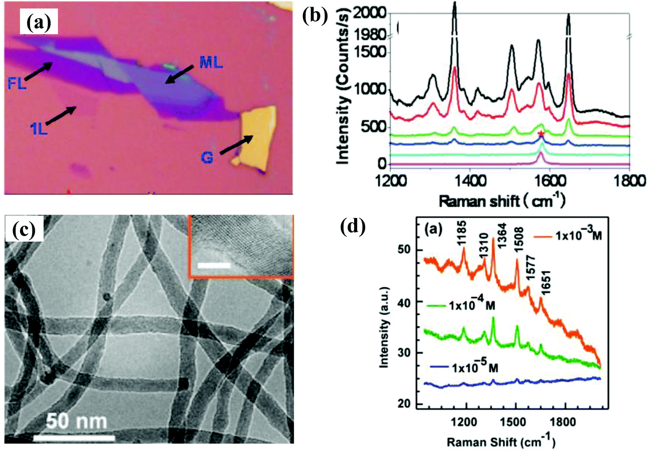 | ||
| Fig. 4 (a) Optical image of graphene (single layer, few layers, and multilayer) and graphite. (b) SERS spectrum of Rhodamine 6G (R6G) molecules adsorbed on monolayer graphene (blue line), multilayer graphene (green line), and graphite (red line) substrates. Reproduced with permission from ref. 51 (Copyright © 2010, American Chemical Society). (c) TEM image of Si nanowires; the inset shows the HRTEM image of a typical Si nanowire. (d) SERS spectra of the R6G molecules adsorbed onto the Si nanowire substrate. Reproduced with permission from ref. 55 (Copyright © 2017, American Chemical Society). | ||
 | ||
| Fig. 5 (a) Optical image of 2D NbS2 on SiO2/Si substrate. (b) SERS spectra of different concentrations of methylene blue (MeB) molecules adsorbed on NbS2 substrate; the inset is the SERS mapping of a single NbS2 flake. Reproduced with permission from ref. 60 (Copyright © 2019, American Chemical Society). (c) SEM image of the MoS2 nanoflowers. (d) SERS spectra of 4-mercaptopyridine (4-MPy) adsorbed on MoS2 with different interlayer distances. Reproduced with permission from ref. 61 (Copyright © 2020, American Chemical Society). (e) Schematic showing the work principle of ReS2 nanosheets as SERS platform. Reproduced with permission from ref. 64 (Copyright © 2018 WILEY-VCH Verlag GmbH & Co. KGaA, Weinheim). | ||
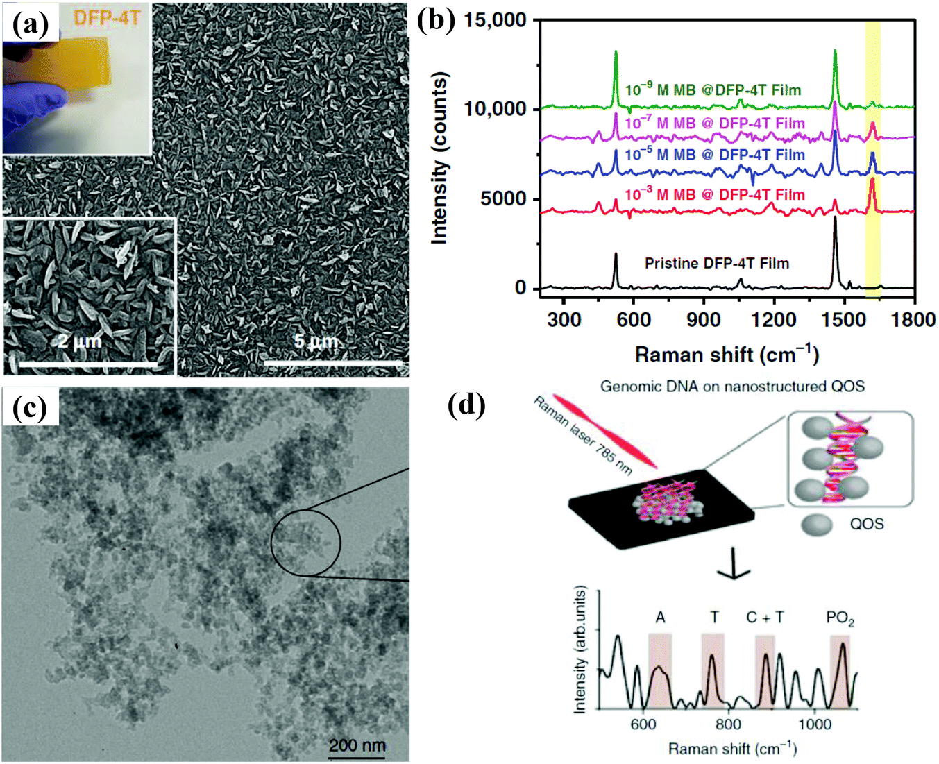 | ||
| Fig. 6 (a) SEM image of the DFP-4T film; the top inset shows the optical image of the DFP-4T film. (b) SERS spectra of MB molecules adsorbed on nanostructured DFP-4T film at different concentrations. Reproduced with permission from ref. 65 (Copyright © 2019, the author(s)). (c) TEM image of a quantum organic semiconductor. (d) The schematic of genomic DNA detection on a quantum organic semiconductor. Reproduced with permission from ref. 66 (Copyright © 2020, the author(s)). | ||
3 Approaches for enhancing the SERS performance of semiconductor substrates
Despite the semiconductor materials discussed in the previous section displaying SERS activity, the SERS performance is usually poor for most pure semiconductor materials.67–70 Therefore, how to obtain highly sensitive semiconductor substrates is the essential issue to promote its practical applications. In this section, we discuss several strategies to enhance the SERS performance of semiconductor substrates mainly in the aspect of regulation mechanism. Table 1 shows the SERS performance of pure semiconductor nanocrystals and semiconductor substrates using improvement strategies, from which we can see that these strategies can effectively enhance the SERS performance of semiconductor substrates.| SERS substrate | Improvement strategy | Probes | EF | Ref. | |
|---|---|---|---|---|---|
| Pure semiconductor materials | TiO2 nanoparticles | — | 4-MBA | 1–102 | 67 |
| ZnO nanocrystal | — | 4-MPy | 103 | 68 | |
| CuO nanocrystal | — | 4-MPy | 102 | 69 | |
| Graphene | — | Dye molecules | 2–17 | 51 | |
| CdS nanoparticles | — | 4-MPy | 102 | 70 | |
| Performance improvement | Hollow multi-shelled V2O5 microstructure | Morphology design | MB | 1.18 × 10⁶ | 86 |
| Sea urchins-like MoO3 | Morphology design | R6G | 105 | 87 | |
| Graphene quantum dots | Size adjustment | Dye molecules | 2730 | 92 | |
| ZnO superstructure | Size adjustment | 4-MPy | 105 | 96 | |
| Ga-doped ZnO nanoparticles | Defect engineering | MPy | 6.66 × 10⁴ | 107 | |
| W18O49 nanowires | Defect engineering | R6G | 3.4 × 10⁵ | 107 | |
| Amorphous TiO2 Nanosheets | Crystallinity | 4-MBA | 1.86 × 10⁶ | 29 | |
3.1 Morphology design
The Raman enhancement of noble metals strongly depends on LSPR, so structural design is an effective method to regulate their plasma properties and construct “hot spots”. For example, the tip metal nanostructures with a small radius of curvature are prone to generating strong local electromagnetic fields due to the “lightning rod” effect.71 Some metal nanostructures with rough surface or tiny nanogaps also contain abundant “hot spots”.72–74 Similar to noble metal nanostructures, the plasmon resonance of semiconductors can be manipulated by morphology design and optimization to enhance the SERS performance.75 Benefiting from the abundant species and mature synthesis technology, various semiconductor nanostructures ranging from 0D (quantum dot, nanocrystalline),68,76 1D (nanowire, nanorod, nanocone),77,78 and 2D (nanoplate, nanodisk)79,80 to 3D (nanocage, nanoflower, nanoarray)81,82 have been developed. Fu et al. synthesized α-Fe3O4 nanocrystals with different morphologies and explored the influence of morphology on SERS performance. They found the enhancement ability was nanospheres > nanospindles > nanocubes, indicating the great influence of morphology on SERS activity.83 Semiconductor nanostructures also display morphology-dependent local surface plasmon resonance effect in the near-infrared region.84 The morphology of the semiconductor substrate mainly affects its SERS performance through the following aspects:(1) Morphology design may induce specific structural resonance or enhanced light–matter interaction to boost the Raman signal. Singh et al. synthesized MoS2 nanoflowers by the hydrothermal method (Fig. 7a). They proposed that multi-reflection can take place under the incident light due to the existence of numerous nanosheets in the nanoflowers, which can enhance the electromagnetic radiation.85 Ji et al. used hollow multi-shelled V2O5 microstructures as the SERS substrate, as shown in Fig. 7c and d. This platform exhibited excellent SERS performance because the unique structure possessed light-trapping effect and generated high electric field between inner and outer shells (Fig. 7e).86
 | ||
| Fig. 7 (a) SEM image of MoS2 nanoflowers. Reproduced with permission from ref. 85 (Copyright © 2020 Elsevier B.V. All rights reserved). (b) SEM image of a sea urchin-like MoO3 nanostructure. Reproduced with permission from ref. 87 (Copyright © 2019, Royal Society of Chemistry). (c) Schematic demonstrating the microstructure of hollow multi-shelled V2O5. (d) SEM image of a hollow multi-shelled V2O5 microstructure; the inset is the enlarged SEM image. (e) Electromagnetic near-field distribution of single hollow multi-shelled V2O5 microstructure under 532 nm excitation. Reproduced with permission from ref. 86 (Copyright © 2021 Wiley-VCH GmbH). | ||
(2) Some unique structures, especially for sharp tip structure and tiny nanogaps, are conducive to the generation of Raman “hot spots”, which can amplify the Raman signal effectively. Fig. 7b shows the SEM image of a sea urchin-like MoO3 nanostructure prepared by a chemical bath deposition method, which exhibits better SERS performance than the traditional 1D MoO3 nanorod due to the existence of abundant sharp tips.87 Ren et al. found that MoO3/MoO2 nanosheets with rough surface had excellent SERS performance due to the generation of strong electric field in the gap between adjacent MoO3.88 Therefore, we can carefully design the morphology of semiconductor substrates based on the above guidelines to improve their SERS performance.
In addition, rational morphology design can make SERS substrates provide more adsorption sites for target molecules, so the SERS performance can be further improved due to the concentration effect. For example, Singh et al. found that MoS2 nanoflowers with large surface areas possess better SERS performance.85
3.2 Size adjustment
The size adjustment of semiconductors is also usually utilized to improve their SERS performance.89,90 In this section, we analyze the effect of reducing the size of semiconductors to quantum dots and larger size semiconductor particles on SERS performance. The corresponding regulatory mechanism is summarized as follows:(1) The quantization of semiconductor nanoparticles mainly improves SERS performance by optimizing the charge transfer process. When the size of the semiconductor nanoparticles is small enough to be quantum dots (especially when the nanoparticle size is smaller than the exciton Bohr radius), the exciton levels will split due to the quantum confinement effect.67,89 The above phenomenon affects the energy level matching and charge transfer process between the semiconductor and probe molecules by changing the energy level structure of semiconductor nanoparticles, thereby regulating the SERS performance of the semiconductor substrates.91 Furthermore, compared with bulk materials, quantum dots possess larger surface area, allowing more probe molecules to adsorb on the surface. And the electrons on the quantum dots surface are weakly bound and can easily participate in the charge transfer process between the SERS substrate and probe molecules, thus improving SERS ability. Liu et al. prepared graphene quantum dots (P-GQDs) using a chemical vapor deposition method (Fig. 8a) and the size of P-GQDs can be well controlled by the growth temperature.92 Compared with conventional graphene and highly oriented pyrolytic graphite, the P-GQDs exhibited stronger Raman enhancement ability, as shown in Fig. 8b. Interestingly, the SERS performance of P-GQDs showed size dependence, i.e. the P-GQDs with a diameter of 6.2 nm had the largest Raman enhancement due to the energy level matching between probe molecules and P-GQDs (Fig. 8c). Ta2O5 superstructure composed of numerous Ta2O5 quantum dots was synthesized via a simple hydrothermal method by Yang et al. Benefiting from the molecular resonance and charge transfer resonance, the Ta2O5 superstructure SERS substrate presented better Raman enhancement ability than bulk Ta2O5.93
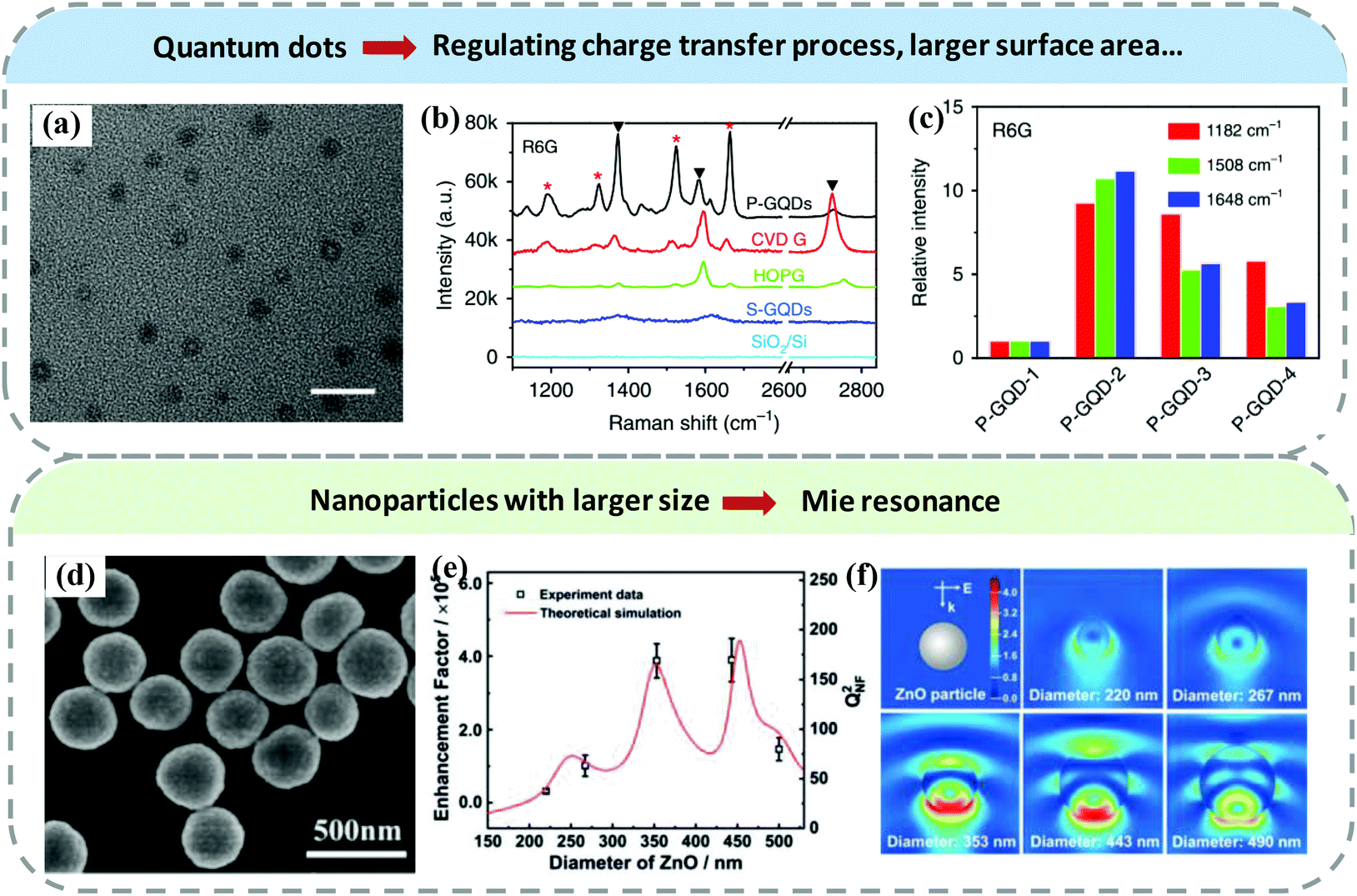 | ||
| Fig. 8 (a) TEM image of graphene quantum dots. The scale bar is 20 nm. (b) SERS spectra of R6G molecules adsorbed on SiO2/Si, GQDs prepared by solution method (S-GQDs), highly oriented pyrolytic graphite (HOPG), graphene (CVD G), and P-GQDs. (c) The comparison of Raman enhancement ability of P-GQDs with different diameters. Reproduced with permission from ref. 92 (Copyright © 2018, Springer Nature). (d) SEM image of ZnO superstructure. (e) The enhancement factor of different sizes of a ZnO superstructure. (f) Electric field distribution of ZnO superstructure with different diameters. Reproduced with permission from ref. 96 (Copyright © 2019 Wiley-VCH Verlag GmbH & Co. KGaA, Weinheim). | ||
(2) Semiconductor nanoparticles with large size and high refractive index can generate Mie resonance under suitable excitation wavelength.94,95 Actually, one of the reasons for the low SERS sensitivity of most semiconductor materials is the lack of electromagnetic enhancement. For semiconductor materials, the Mie resonance effect can generate local electromagnetic field enhancement to improve the SERS performance. For example, Ji et al. synthesized submicrometer-sized spherical ZnO superstructures as a SERS substrate (Fig. 8d) and obtained Mie resonance on this substrate by tuning the superstructure size. They found that the enhancement factor of this ZnO superstructure SERS substrate exhibits obvious size dependence, as shown in Fig. 8e. The near-field electric field distribution of the ZnO superstructure with different diameters in Fig. 8f further shows the size dependence effect.96 Therefore, we can realize electromagnetic enhancement on semiconductors by choosing suitable semiconductor materials and carefully tuning their size and structures.
3.3 Defect engineering
Defect engineering, as the most commonly used approach to improve the SERS performance of semiconductor materials, has been systematically studied. Currently, researchers mainly introduce defects in semiconductor materials through producing oxygen vacancies and element doping.97–99(1) On the one hand, defect engineering can promote the charge transfer process between the semiconductor substrates and probe molecules because appropriate defects can change the energy level structure of the semiconductors by forming the surface defect state energy level. Making oxygen vacancies is an effective approach to obtain semiconductor substrates with great SERS performance. Researchers have successfully introduced oxygen vacancies in semiconductor materials via various methods, such as ion irradiation, lithium metal grinding reduction, and high temperature annealing under reducing gas atmosphere, etc.100–102 Typically, Fan et al. employed WO3−x rich in oxygen vacancies as a SERS substrate.103 The oxygen vacancy played a critical role in improving the SERS performance of the WO3−x substrate because it could form surface defect levels between the CB and VB of WO3−x. The additional resonance caused by the oxygen vacancy resulted in the remarkable SERS performance (Fig. 9a and b). Conversely, Zheng et al. obtained SERS-active MoSxOy semiconductor substrate by oxygen incorporation.104 The improved SERS performance was also attributed to the regulation of semiconductor energy levels by the oxygen incorporation process, which can promote the charge transfer process. Element doping (Co, Mg, Cu, H, etc.) is also adopted to improve the SERS performance. Zhou et al. synthesized Cu-doped SnO2-NiO semiconductor SERS substrate and achieved very high enhancement factor (1.46 × 10¹⁰)105 (Fig. 9c). They proved that Cu doping was beneficial to charge transfer resonance, Fig. 9d shows the energy level diagram of the probe molecules and SERS substrate.
 | ||
| Fig. 9 (a) SERS spectra of R6G molecules adsorbed on WO3−x substrate at different concentrations. (b) Schematic showing the energy level diagram of R6G on WO3−x and the charge transfer process in this system. Reproduced with permission from ref. 103 (Copyright © 2019 WILEY-VCH Verlag GmbH & Co. KGaA, Weinheim). (c) SERS spectra of copper phthalo-cyanine (CuPc) molecules on Si(I), SnO2 (II), SnO2-NiO (III), and Cu-doped SnO2-NiO (IV) substrates. (d) Schematic presenting the energy level diagram of CuPc on Cu-doped SnO2-NiO and the charge transfer process. Reproduced with permission from ref. 105 (Copyright © 2021 Wiley-VCH GmbH). (e) Electron paramagnetic resonance (EPR) spectra of the W18O49 and WO3 mesocrystals. (f) UV-vis spectra of W18O49 and WO3 mesocrystals. Reproduced with permission from ref. 25 (Copyright © 2021, American Chemical Society). (g) FTIR absorption spectra of Ga-doped ZnO nanoparticles combined with the UV-vis-NIR absorption spectra. (h) SERS spectra of MPy on Ga-doped ZnO substrate with different doping ratios. Reproduced with permission from ref. 107 (Copyright © 2021, American Chemical Society). | ||
(2) On the other hand, defect engineering can introduce LSPR contribution in the semiconductor materials. It has been reported that defects can modulate the carrier concentration of semiconductors, so proper defects can adjust the LSPR peak of the semiconductors in the far-infrared light region to the near-infrared or even visible light region, thereby introducing LSPR in the semiconductor materials. Zhao et al. first reported the surface plasmon resonance phenomenon in the doped semiconductors in 2009, which promoted the study of electromagnetic enhancement contribution in semiconductor materials to SERS.106 Ye et al. obtained an oxygen vacancy-rich W18O49 mesocrystal by a rapid and green microwave synthetic method. They found that free electrons significantly increased because of the existence of a vast number of oxygen vacancies (Fig. 9e). Therefore, W18O49 exhibited a strong LSPR effect in the 400–800 nm range25 (Fig. 9f). Apart from creating oxygen vacancies, by introducing gallium doping into ZnO nanoparticles, Wang et al. obtained Ga-doped ZnO nanoparticles with obvious surface plasmon resonance absorption in the visible-NIR region.107 They found that electromagnetic enhancement played a key role in the Raman enhancement for this SERS substrate. And proper doping concentration was conducive to the increase of carrier concentration, resulting in stronger surface plasmon resonance absorption and SERS enhancement (Fig. 9g and h). Therefore, utilizing rational defect engineering, we can improve the SERS performance of semiconductor substrates by promoting the charge transfer process and introducing the LSPR effect.
3.4 Crystallinity
Different crystallinity of semiconductors will also affect the SERS performance by regulating the charge transfer process.23,108 Usually, the crystalline semiconductors have ordered and periodic lattice structures, which may restrict the electron transfer. In contrast, the long-range disordered structure of amorphous semiconductors facilitates the electron transfer process. Wang et al. systematically studied this effect. In 2017, they first observed ultrahigh SERS activity in amorphous ZnO nanocages (a-ZnO NCs).109 They explored the possible enhancement mechanism of a-ZnO NCs using density functional theory simulations. Compared with crystalline ZnO nanocages (c-ZnO NCs), the electronic state of a-ZnO NCs was a metastable state, so the surface electrons were easily transferred, resulting in a more effective charge transfer process. Based on this finding, they further developed amorphous Rh3S6 as a highly sensitive SERS substrate (Fig. 10a).110 They proposed that the excellent sensitivity could be ascribed to the quasi-resonance Raman effect and multiple light scattering, as shown in Fig. 10b. In 2019, they studied the SERS performance of amorphous TiO2 nanosheets (a-TiO2 NSs) and crystalline TiO2 nanosheets (c-TiO2 NSs), and the former exhibited stronger SERS activity. Fig. 10c clearly shows the SERS spectra comparison of a-TiO2 NSs and c-TiO2 NSs for 4-MBA molecules. On the one hand, they found that a-TiO2 NSs possessed relatively narrow band gap and higher electronic density of states, which facilitated stronger vibronic coupling. And the improved vibronic coupling could promote the charge transfer resonance, as shown in Fig. 10d. In addition, the a-TiO2 NSs had higher electrostatic potential because of the existence of abundant low coordination Ti atoms and oxygen defects, and this can also induce larger charge transfer.29 Another amorphous semiconductor nanomaterials, such as HxMoO3 quantum dots and M(OH)x (M = Fe, Co, Ni) also displayed excellent SERS performance.111–113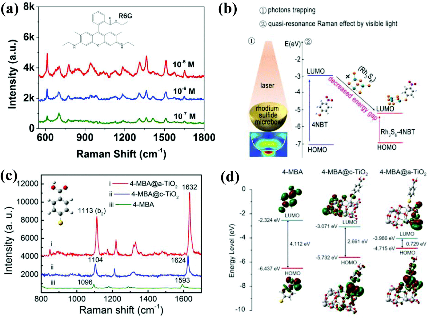 | ||
| Fig. 10 (a) SERS spectra of R6G molecules adsorbed on amorphous Rh3S6 substrate at different concentrations. (b) Enhancement mechanism of the Rh3S6 microbowl substrate. Reproduced with permission from ref. 110 (Copyright © 2018 The Author(s)). (c) SERS spectra of 4-MBA on amorphous and crystalline TiO2 nanosheets. (d) The energy level diagram of 4-MBA, 4-MBA@ crystalline TiO2, and 4-MBA@ amorphous TiO2. Reproduced with permission from ref. 29 (Copyright © 2019, American Chemical Society). | ||
3.5 Phase structure
Some semiconductor materials have multiple phase structures, so studying the phase structure dependence of SERS performance is helpful in optimizing the SERS activity.114,115 Typically, the MoX2 (X = S, Se, etc.) involves semiconducting 2H-phase and metallic 1T-phase, and they present different electrochemical properties. Yin et al. demonstrated that the SERS performance of 1T-MoX2 (X = S, Se) is superior to 2H-MoX2, as shown in Fig. 11a. According to experimental results and theoretical analysis, they speculated the possible reason for the better SERS performance of 1T-MoX2 (taking MoSe2 as example) (Fig. 11b), i.e. no extra energy was required when the electrons jumped from Fermi energy level of the 1T-MoSe2 to the HOMO level of molecules, resulting in more efficient charge transfer process than 2H-MoSe2 (electrons required 0.065 eV energy when transferred from top of the valence band (TVB) of 2H-MoSe2 to HOMO level of molecules).116 TiO2 is also a typical multiple phase material (anatase, rutile, and brookite phase). Yang et al. compared the SERS performance of TiO2 nanoparticles with different phase structure. They found that TiO2 nanoparticles with mixed phase structure (anatase phase: 85%, rutile phase: 15%) exhibited optimal SERS performance. Fig. 11c displays the TEM image of the mixed phase TiO2. In this mixed phase structure TiO2, the holes tend to transfer from anatase to rutile phase while the electrons follow a reverse transfer path (Fig. 11d). Therefore, apart from the charge transfer enhancement of intrinsic anatase TiO2, the synergy between the two phases provides additional charge transfer.117 Therefore, in addition to focusing on the impact of some main factors (morphology, size, defect, and crystallinity) on the SERS performance, we can also optimize its SERS performance by selecting appropriate semiconductor phase structure.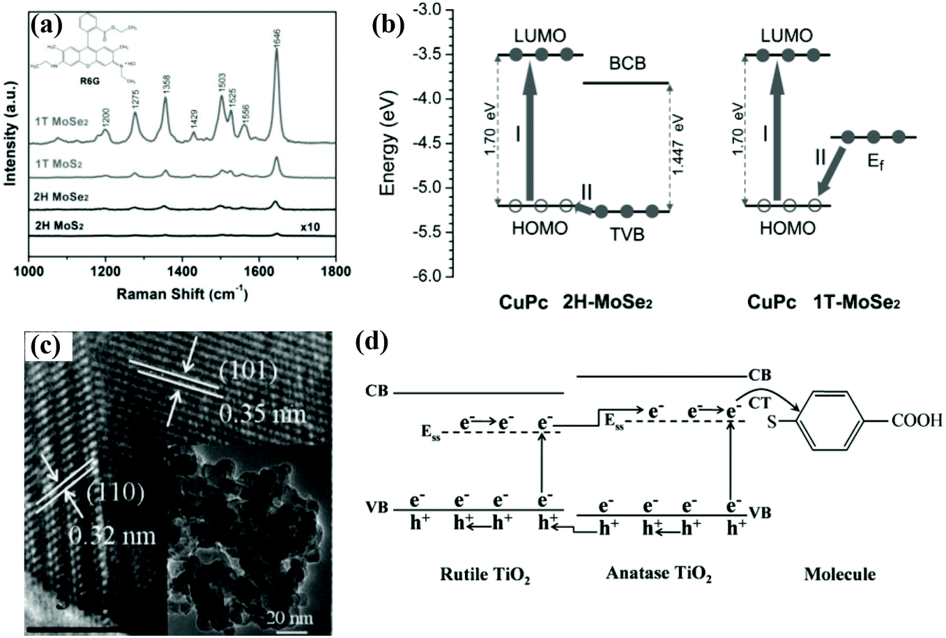 | ||
| Fig. 11 (a) SERS spectra of R6G on 1T MoSe2, 1T MoS2, 2H MoSe2, and 2H MoS2 substrates. (b) The energy level diagram and charge transfer process of CuPc molecules on 2H and 1T MoSe2. Reproduced with permission from ref. 116 (Copyright © 2017 WILEY-VCH Verlag GmbH & Co. KGaA, Weinheim). (c) High-resolution TEM image of TiO2 nanoparticles; the inset is a low magnification TEM image. (d) The charge transfer process of probe molecules adsorbed on the mixed phase TiO2 nanoparticles. Reproduced with permission from ref. 117 (Copyright © 2015 John Wiley & Sons, Ltd). | ||
4 Conclusions and outlook
As a powerful spectroscopic technique with the advantages of high sensitivity, fingerprint specificity, and fast and non-destructive detection, SERS has shown great application potential in various fields. The construction of high-performance SERS substrates is key to promoting their practical applications. For a long time, SERS substrates based on noble metal materials have been dominant. However, in view of the bottleneck of noble metal SERS substrates, semiconductor SERS substrates have been developed and extensively studied. In this review, we summarized several main types of semiconductor SERS substrates, as well as the strategies to further improve the SERS performance of semiconductor substrates.Although semiconductor SERS substrates possess obvious merits compared to noble metal SERS substrates, and a large number of SERS-active semiconductor nanomaterials have been successfully fabricated with the efforts of researchers, there are still some challenges as follows: (1) The most fatal shortcoming of semiconductor SERS substrates is the weak Raman enhancement because chemical enhancement plays a major role in semiconductors. At present, the SERS sensitivity of most semiconductor substrates is low, which is difficult to meet the needs of practical applications. (2) Most studies improved SERS performance of semiconductor substrates by enhancing the charge transfer resonance, and the improvement ability is limited. Research on boosting the SERS ability of semiconductors by regulating the electromagnetic enhancement is relatively lacking. (3) Currently, the types of SERS-active semiconductor materials are limited because the research started relatively late. More potential semiconductor materials are worth developing. (4) The Raman enhancement mechanism of semiconductor SERS substrates is complicated and the research on it remains to be deepened and improved.
Therefore, developing novel SERS-active semiconductor materials, introducing electromagnetic enhancement, or even utilizing the synergistic effects of the CM and EM to boost the Raman enhancement ability, and elucidating the SERS mechanism by effective means are meaningful to promote the development and practical applications of high-performance semiconductor SERS substrates. Fig. 12 shows the challenges and possible solutions in the field of semiconductor SERS.
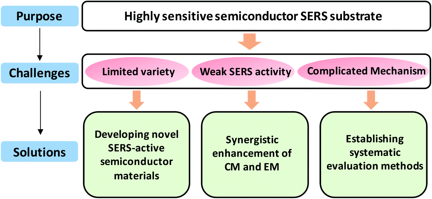 | ||
| Fig. 12 The challenges and possible solutions in the field of semiconductor SERS. | ||
Author contributions
Xuejiao Wang: Conceptualization, formal analysis, data curation, investigation, writing – original draft. Erjin Zhang: Writing – review and editing, funding acquisition, project administration. Huimin Shi: Formal analysis, data curation. Yufeng Tao: Formal analysis, data curation. Xudong Ren: Writing – review and editing, supervision, funding acquisition.Conflicts of interest
There are no conflicts to declare.Acknowledgements
We gratefully acknowledge the financial support from the Natural Science Foundation of Jiangsu (BK20210746, BK20210781) and the National Natural Science Foundation of China (No. 52102259).References
- M. Fleischmann, P. J. Hendra and A. J. Mcquillan, Chem. Phys. Lett., 1974, 26, 163–166 CrossRef CAS.
- J. Perumal, Y. Wang, A. B. E. Attia, U. Dinish and M. Olivo, Nanoscale, 2021, 13, 553–580 RSC.
- Y. X. Leong, Y. H. Lee, C. S. L. Koh, G. C. Phan-Quang, X. Han, I. Y. Phang and X. Y. Ling, Nano Lett., 2021, 21, 2642–2649 CrossRef CAS PubMed.
- Y. C. Kao, X. Han, Y. H. Lee, H. K. Lee, G. C. Phan-Quang, C. L. Lay, H. Y. F. Sim, V. J. X. Phua, L. S. Ng, C. W. Ku, T. C. Tan, I. Y. Phang, N. S. Tan and X. Y. Ling, ACS Nano, 2020, 14, 2542–2552 CrossRef CAS PubMed.
- H. Feng, Q. Fu, W. Du, R. Zhu, X. Ge, C. Wang, Q. Li, L. Su, H. Yang and J. Song, ACS Nano, 2021, 15, 3402–3414 CrossRef CAS PubMed.
- J. Shan, Y. Zhang, J. Wang, T. Ren, M. Jin and X. Wang, J. Hazard. Mater., 2020, 400, 123202 CrossRef CAS PubMed.
- C. S. L. Koh, H. K. Lee, X. Han, H. Y. F. Sim and X. Y. Ling, Chem. Commun., 2018, 54, 2546–2549 RSC.
- L. Wu, H. Pu, L. Huang and D.-W. Sun, Food Chem., 2020, 328, 127105 CrossRef CAS PubMed.
- Y. Chen, H. Liu, Y. Tian, Y. Du, Y. Ma, S. Zeng, C. Gu, T. Jiang and J. Zhou, ACS Appl. Mater. Interfaces, 2020, 12, 14386–14399 CrossRef CAS PubMed.
- A. Alyami, A. Mirabile and D. Iacopino, Heritage Sci., 2019, 7, 1–10 CrossRef CAS.
- X. X. Han, W. Ji, B. Zhao and Y. Ozaki, Nanoscale, 2017, 9, 4847–4861 RSC.
- V. Rajput, R. K. Gupta and J. Prakash, J. Mater. Chem. C, 2022, 10, 73–95 RSC.
- G. Demirel, H. Usta, M. Yilmaz, M. Celik, H. A. Alidagi and F. Buyukserin, J. Mater. Chem. C, 2018, 6, 5314–5335 RSC.
- W. Ji, B. Zhao and Y. Ozaki, J. Raman Spectrosc., 2016, 47, 51–58 CrossRef CAS.
- R. Haldavnekar, K. Venkatakrishnan and B. Tan, Nat. Commun., 2018, 9, 1–18 CrossRef CAS PubMed.
- B. Yang, S. Jin, S. Guo, Y. Park, L. Chen, B. Zhao and Y. M. Jung, ACS Omega, 2019, 4, 20101–20108 CrossRef CAS PubMed.
- L. Tao, K. Chen, Z. Chen, C. Cong, C. Qiu, J. Chen, X. Wang, H. Chen, T. Yu and W. Xie, J. Am. Chem. Soc., 2018, 140, 8696–8704 CrossRef CAS PubMed.
- J. Yao, Y. Quan, R. Gao, J. Li, L. Chen, Y. Liu, J. Lang, H. Shen, Y. Wang and J. Yang, Langmuir, 2019, 35, 8921–8926 CrossRef CAS PubMed.
- Y. Quan, J. Yao, S. Yang, L. Chen, Y. Liu, J. Lang, H. Zeng, J. Yang and M. Gao, J. Hazard. Mater., 2020, 391, 122222 CrossRef CAS PubMed.
- X. Wang, G. She, H. Xu, L. Mu and W. Shi, Sens. Actuators, B, 2014, 193, 745–751 CrossRef CAS.
- J. R. Lombardi and R. L. Birke, J. Phys. Chem. C, 2014, 118, 11120–11130 CrossRef CAS.
- H. K. Lee, Y. H. Lee, C. S. L. Koh, G. C. Phan-Quang, X. Han, C. L. Lay, H. Y. F. Sim, Y. C. Kao, Q. An and X. Y. Ling, Chem. Soc. Rev., 2019, 48, 731–756 RSC.
- X. Wang and L. Guo, Angew. Chem., Int. Ed., 2020, 59, 4231–4239 CrossRef CAS PubMed.
- J. M. Luther, P. K. Jain, T. Ewers and A. P. Alivisatos, Nat. Mater., 2011, 10, 361–366 CrossRef CAS PubMed.
- Y. Ye, C. Chen, W. Li, X. Guo, H. Yang, H. Guan, H. Bai, W. Liu and G. Xi, Anal. Chem., 2021, 93, 3138–3145 CrossRef CAS PubMed.
- D. Maznichenko, K. Venkatakrishnan and B. Tan, J. Phys. Chem. C, 2012, 117, 578–583 CrossRef.
- A. I. Kuznetsov, A. E. Miroshnichenko, M. L. Brongersma, Y. S. Kivshar and B. Luk'yanchuk, Science, 2016, 354 DOI:10.1126/science.aag2472.
- S. Hayashi, R. Koh, Y. Ichiyama and K. Yamamoto, Phys. Rev. Lett., 1988, 60, 1085–1088 CrossRef CAS PubMed.
- X. Wang, W. Shi, S. Wang, H. Zhao, J. Lin, Z. Yang, M. Chen and L. Guo, J. Am. Chem. Soc., 2019, 141, 5856–5862 CrossRef CAS PubMed.
- B. Yang, Y. Wang, S. Guo, S. Jin, E. Park, L. Chen and Y. M. Jung, Bull. Korean Chem. Soc., 2021, 42, 1411–1418 CrossRef CAS.
- A. Musumeci, D. Gosztola, T. Schiller, N. M. Dimitrijevic, V. Mujica, D. Martin and T. Rajh, J. Am. Chem. Soc., 2009, 131, 6040–6041 CrossRef CAS PubMed.
- Y. Liu, H. Ma, X. X. Han and B. Zhao, Mater. Horiz., 2021, 8, 370–382 RSC.
- H. Wu, H. Wang and G. Li, Analyst, 2017, 142, 326–335 RSC.
- T. Takagahara and K. Takeda, Phys. Rev. B: Condens. Matter Mater. Phys., 1992, 46, 15578–15581 CrossRef CAS PubMed.
- L. E. Brus, J. Chem. Phys., 1984, 80, 4403–4409 CrossRef CAS.
- S. E. Bell, G. Charron, E. Cortés, J. Kneipp, M. L. de la Chapelle, J. Langer, M. Prochazka, V. Tran and S. Schlücker, Angew. Chem., Int. Ed., 2020, 59, 5454–5462 CrossRef CAS PubMed.
- H. Yamada, Y. Yamamoto and N. Tani, Chem. Phys. Lett., 1982, 86, 397–400 CrossRef CAS.
- H. Yamada and Y. Yamamoto, Surf. Sci., 1983, 134, 71–90 CrossRef CAS.
- C. Liu, Q. Song, J. Chen, X. Li, J. Cai, Z. Lu, W. Li, N. X. Fang and S. P. Feng, Adv. Mater. Interfaces, 2019, 6, 1900534 CrossRef.
- E. Proniewicz, A. Tata, A. Wojcik, M. Starowicz, J. Pacek and M. Molenda, Phys. Chem. Chem. Phys., 2020, 22, 28100–28114 RSC.
- J. Lin, J. Yu, O. U. Akakuru, X. Wang, B. Yuan, T. Chen, L. Guo and A. Wu, Chem. Sci., 2020, 11, 9414–9420 RSC.
- B. P. Majee and A. K. Mishra, Mater. Res. Express, 2020, 6, 1250j1 CrossRef.
- H. A. O. Wen, Mol. Phys., 1996, 88, 281–290 CrossRef CAS.
- Q. Liu, L. Jiang and L. Guo, Small, 2014, 10, 48–51 CrossRef CAS PubMed.
- H. Zhang, S. Huang, X. Yang, R. Yuan and Y. Chai, Sens. Actuators, B, 2021, 343, 130142 CrossRef CAS.
- L. Yang, Y. Peng, Y. Yang, J. Liu, Z. Li, Y. Ma, Z. Zhang, Y. Wei, S. Li, Z. Huang and N. V. Long, ACS Appl. Nano Mater., 2018, 1, 4516–4527 CrossRef CAS.
- X. Li, Y. Shang, J. Lin, A. Li, X. Wang, B. Li and L. Guo, Adv. Funct. Mater., 2018, 28, 1801868 CrossRef.
- J. Li, H. Bai, J. Zhai, W. Li, W. Fan and G. Xi, Chem. Commun., 2019, 55, 4679–4682 RSC.
- L. Yang, Y. Peng, Y. Yang, J. Liu, H. Huang, B. Yu, J. Zhao, Y. Lu, Z. Huang, Z. Li and J. R. Lombardi, Adv. Sci., 2019, 6, 1900310 CrossRef PubMed.
- L. Yang, Y. Wei, Y. Song, Y. Peng, Y. Yang and Z. Huang, Mater. Des., 2020, 193, 108808 CrossRef CAS.
- X. Ling, L. Xie, Y. Fang, H. Xu, H. Zhang, J. Kong, M. S. Dresselhaus, J. Zhang and Z. Liu, Nano Lett., 2009, 10, 553–561 CrossRef PubMed.
- J. Seo, J. Lee, Y. Kim, D. Koo, G. Lee and H. Park, Nano Lett., 2020, 20, 1620–1630 CrossRef CAS PubMed.
- X. Pan, L. Li, H. Lin, J. Tan, H. Wang, M. Liao, C. Chen, B. Shan, Y. Chen and M. Li, Biosens. Bioelectron., 2019, 145, 111713 CrossRef CAS PubMed.
- S. A. Ghopry, M. A. Alamri, R. Goul, R. Sakidja and J. Z. Wu, Adv. Opt. Mater., 2019, 7, 1801249 CrossRef.
- H. Cui, S. Li, S. Deng, H. Chen and C. Wang, ACS Sens., 2017, 2, 386–393 CrossRef CAS PubMed.
- E. Er, H.-L. Hou, A. Criado, J. Langer, M. Möller, N. Erk, L. M. Liz-Marzán and M. Prato, Chem. Mater., 2019, 31, 5725–5734 CrossRef CAS.
- D. Yan, W. Qiu, X. Chen, L. Liu, Y. Lai, Z. Meng, J. Song, Y. Liu, X.-Y. Liu and D. Zhan, J. Phys. Chem. C, 2018, 122, 14467–14473 CrossRef CAS.
- M. Li, Y. Gao, X. Fan, Y. Wei, Q. Hao and T. Qiu, Nanoscale Horiz., 2021, 6, 186–191 RSC.
- C. Weng, Y. Luo, B. Wang, J. Shi, L. Gao, Z. Cao and G. Duan, J. Mater. Chem. C, 2020, 8, 14138–14145 RSC.
- X. Song, Y. Wang, F. Zhao, Q. Li, H. Q. Ta, M. H. Rummeli, C. G. Tully, Z. Li, W. J. Yin, L. Yang, K. B. Lee, J. Yang, I. Bozkurt, S. Liu, W. Zhang and M. Chhowalla, ACS Nano, 2019, 13, 8312–8319 CrossRef CAS PubMed.
- X. Li, S. Guo, J. Su, X. Ren and Z. Fang, ACS Appl. Mater. Interfaces, 2020, 12, 28474–28483 CrossRef CAS PubMed.
- L. Tao, K. Chen, Z. Chen, C. Cong, C. Qiu, J. Chen, X. Wang, H. Chen, T. Yu, W. Xie, S. Deng and J. B. Xu, J. Am. Chem. Soc., 2018, 140, 8696–8704 CrossRef CAS PubMed.
- P. Karthick Kannan, P. Shankar, C. Blackman and C. H. Chung, Adv. Mater., 2019, 31, 1803432 CrossRef PubMed.
- P. Miao, J. K. Qin, Y. Shen, H. Su, J. Dai, B. Song, Y. Du, M. Sun, W. Zhang, H. L. Wang, C. Y. Xu and P. Xu, Small, 2018, 14, e1704079 CrossRef PubMed.
- G. Demirel, R. L. Gieseking, R. Ozdemir, S. Kahmann, M. A. Loi, G. C. Schatz, A. Facchetti and H. Usta, Nat. Commun., 2019, 10, 1–9 CrossRef PubMed.
- S. Ganesh, K. Venkatakrishnan and B. Tan, Nat. Commun., 2020, 11, 1–15 Search PubMed.
- X. Xue, W. Ji, Z. Mao, H. Mao, Y. Wang, X. Wang, W. Ruan, B. Zhao and J. R. Lombardi, J. Phys. Chem. C, 2012, 116, 8792–8797 CrossRef CAS.
- Y. Wang, W. Ruan, J. Zhang, B. Yang, W. Xu, B. Zhao and J. R. Lombardi, J. Raman Spectrosc., 2009, 40, 1072–1077 CrossRef CAS.
- Y. Wang, H. Hu, S. Jing, Y. Wang, Z. Sun, B. Zhao, C. Zhao and J. R. Lombardi, Anal. Sci., 2007, 23, 787–791 CrossRef CAS PubMed.
- Y. Wang, Z. Sun, Y. Wang, H. Hu, B. Zhao, W. Xu and J. R. Lombardi, Spectrochim. Acta, Part A, 2007, 66, 1199–1203 CrossRef PubMed.
- T. Wang, S. Wang, Z. Cheng, J. Wei, L. Yang, Z. Zhong, H. Hu, Y. Wang, B. Zhou and P. Li, Chem. Eng. J., 2021, 424, 130323 CrossRef CAS.
- L. Wang, S. Patskovsky, B. Gauthier-Soumis and M. Meunier, Small, 2022, 2105209 CrossRef CAS PubMed.
- Z. Lao, Y. Zheng, Y. Dai, Y. Hu, J. Ni, S. Ji, Z. Cai, Z. J. Smith, J. Li and L. Zhang, Adv. Funct. Mater., 2020, 30, 1909467 CrossRef CAS.
- Q. Zhao, H. Yang, B. Nie, Y. Luo, J. Shao and G. Li, ACS Appl. Mater. Interfaces, 2022, 14, 3580–3590 CrossRef PubMed.
- C. Qiu, Y. Bao, N. L. Netzer and C. Jiang, J. Mater. Chem. A, 2013, 1, 8790–8797 RSC.
- H. L. Wu, X. B. Li, C. H. Tung and L. Z. Wu, Adv. Mater., 2019, 31, e1900709 CrossRef PubMed.
- M. Shafi, M. Zhou, P. Duan, W. Liu, W. Zhang, Z. Zha, J. Gao, S. Wali, S. Jiang and B. Man, Sens. Actuators, B, 2022, 131360 CrossRef CAS.
- C. Muehlethaler, A. Odate, J. L. Weyher, I. Dzięcielewski and J. R. Lombardi, Appl. Surf. Sci., 2018, 457, 809–814 CrossRef CAS.
- S. Zhao, H. Wang, L. Niu, W. Xiong, Y. Chen, M. Zeng, S. Yuan and L. Fu, Small, 2021, 17, 2103442 CrossRef CAS PubMed.
- G. Song, W. Gong, S. Cong and Z. Zhao, Angew. Chem., Int. Ed., 2021, 60, 5505–5511 CrossRef CAS PubMed.
- Y. Ye, C. Chen, H. Bai, W. Liu, W. Li, J. Li, W. Yi and G. Xi, Cell Rep. Phys. Sci., 2020, 1, 100031 CrossRef.
- Z. Tian, H. Bai, C. Chen, Y. Ye, Q. Kong, Y. Li, W. Fan, W. Yi and G. Xi, iScience, 2019, 19, 836–849 CrossRef CAS PubMed.
- X. Fu, F. Bei, X. Wang, X. Yang and L. Lu, J. Raman Spectrosc., 2009, 40, 1290–1295 CrossRef CAS.
- W. Li, R. Zamani, P. Rivera Gil, B. Pelaz, M. Ibanez, D. Cadavid, A. Shavel, R. A. Alvarez-Puebla, W. J. Parak, J. Arbiol and A. Cabot, J. Am. Chem. Soc., 2013, 135, 7098–7101 CrossRef CAS PubMed.
- J. Singh, Rishikesh, S. Kumar and R. K. Soni, J. Alloys Compd., 2020, 849, 156502 CrossRef CAS.
- W. Ji, L. Li, J. Guan, M. Mu, W. Song, L. Sun, B. Zhao and Y. Ozaki, Adv. Opt. Mater., 2021, 9, 2101866 CrossRef CAS.
- R. Prabhu B., K. Bramhaiah, K. K. Singh and N. S. John, Nanoscale Adv., 2019, 1, 2426–2434 RSC.
- P. Ren, W. Zhou, X. Ren, X. Zhang, B. Sun, Y. Chen, Q. Zheng, J. Li and W. Zhang, Nanotechnology, 2020, 31, 224002 CrossRef CAS PubMed.
- X. Fu, Y. Pan, X. Wang and J. R. Lombardi, J. Chem. Phys., 2011, 134, 024707 CrossRef PubMed.
- J. Pan, M. Li, Y. Y. Luo, H. Wu, L. Zhong, Q. Wang and G. H. Li, Appl. Surf. Sci., 2015, 333, 34–38 CrossRef CAS.
- S. K. Islam, M. A. Sohel and J. R. Lombardi, J. Phys. Chem. C, 2014, 118, 19415–19421 CrossRef CAS.
- D. Liu, X. Chen, Y. Hu, T. Sun, Z. Song, Y. Zheng, Y. Cao, Z. Cai, M. Cao, L. Peng, Y. Huang, L. Du, W. Yang, G. Chen, D. Wei, A. T. S. Wee and D. Wei, Nat. Commun., 2018, 9, 193 CrossRef PubMed.
- L. Yang, Y. Yang, J. R. Lombardi, Y. Peng and Z. Huang, Appl. Surf. Sci., 2020, 520, 146325 CrossRef CAS.
- P. A. Dmitriev, D. G. Baranov, V. A. Milichko, S. V. Makarov, I. S. Mukhin, A. K. Samusev, A. E. Krasnok, P. A. Belov and Y. S. Kivshar, Nanoscale, 2016, 8, 9721–9726 RSC.
- D. Christie, J. Lombardi and I. Kretzschmar, J. Phys. Chem. C, 2014, 118, 9114–9118 CrossRef CAS.
- W. Ji, L. Li, W. Song, X. Wang, B. Zhao and Y. Ozaki, Angew. Chem., Int. Ed., 2019, 58, 14452–14456 CrossRef CAS PubMed.
- H. Guan, Z. Tian, Q. Kong and G. Xi, Chem. Commun., 2021, 57, 4815–4818 RSC.
- C. Gu, D. Li, S. Zeng, T. Jiang, X. Shen and H. Zhang, Nanoscale, 2021, 13, 5620–5651 RSC.
- Y. Peng, C. Lin, M. Tang, L. Yang, Y. Yang, J. Liu, Z. Huang and Z. Li, Appl. Surf. Sci., 2020, 509, 145376 CrossRef CAS.
- X.-D. Zheng, F. Ren, H.-Y. Wu, W.-J. Qin and C.-Z. Jiang, Nanotechnology, 2018, 29, 155301 CrossRef PubMed.
- Y. Cao, P. Liang, Q. Dong, D. Wang, D. Zhang, L. Tang, L. Wang, S. Jin, D. Ni and Z. Yu, Anal. Chem., 2019, 91, 8683–8690 CrossRef CAS PubMed.
- D. Luo, Z. Zhang, G. Li, S. Cheng, S. Li, J. Li, R. Gao, M. Li, S. Sy and Y.-P. Deng, ACS Nano, 2020, 14, 4849–4860 CrossRef CAS PubMed.
- X. Fan, M. Li, Q. Hao, M. Zhu, X. Hou, H. Huang, L. Ma, O. G. Schmidt and T. Qiu, Adv. Mater. Interfaces, 2019, 6, 1901133 CrossRef CAS.
- Z. Zheng, S. Cong, W. Gong, J. Xuan, G. Li, W. Lu, F. Geng and Z. Zhao, Nat. Commun., 2017, 8, 1993 CrossRef PubMed.
- Y. Zhou, Q. Gu, T. Qiu, X. He, J. Chen, R. Qi, R. Huang, T. Zheng and Y. Tian, Angew. Chem., 2021, 133, 26464–26471 CrossRef.
- Y. Zhao, H. Pan, Y. Lou, X. Qiu, J. Zhu and C. Burda, J. Am. Chem. Soc., 2009, 131, 4253–4261 CrossRef CAS PubMed.
- Y. Wang, M. Zhang, H. Ma, H. Su, A. Li, W. Ruan and B. Zhao, ACS Appl. Mater. Interfaces, 2021, 13, 35038–35045 CrossRef CAS PubMed.
- J. Lin, W. Ren, A. Li, C. Yao, T. Chen, X. Ma, X. Wang and A. Wu, ACS Appl. Mater. Interfaces, 2020, 12, 4204–4211 CrossRef CAS PubMed.
- X. Wang, W. Shi, Z. Jin, W. Huang, J. Lin, G. Ma, S. Li and L. Guo, Angew. Chem., Int. Ed., 2017, 56, 9851–9855 CrossRef CAS PubMed.
- A. Li, J. Lin, Z. Huang, X. Wang and L. Guo, iScience, 2018, 10, 1–10 CrossRef CAS PubMed.
- M. Gao, P. Miao, X. Han, C. Sun, Y. Ma, Y. Gao and P. Xu, Inorg. Chem. Front., 2019, 6, 2318–2324 RSC.
- H. Li, Q. Xu, X. Wang and W. Liu, Small, 2018, 14, e1801523 CrossRef PubMed.
- A. Li, J. Yu, J. Lin, M. Chen, X. Wang and L. Guo, J. Phys. Chem. Lett., 2020, 11, 1859–1866 CrossRef CAS PubMed.
- R. Su, Y. Quan, S. Yang, M. Hu, J. Yang and M. Gao, J. Alloys Compd., 2021, 886, 161268 CrossRef CAS.
- P. Miao, J. Wu, Y. Du, Y. Sun and P. Xu, J. Mater. Chem. C, 2018, 6, 10855–10860 RSC.
- Y. Yin, P. Miao, Y. Zhang, J. Han, X. Zhang, Y. Gong, L. Gu, C. Xu, T. Yao, P. Xu, Y. Wang, B. Song and S. Jin, Adv. Funct. Mater., 2017, 27, 1606694 CrossRef.
- L. Yang, M. Gong, X. Jiang, D. Yin, X. Qin, B. Zhao and W. Ruan, J. Raman Spectrosc., 2015, 46, 287–292 CrossRef CAS.
| This journal is © The Royal Society of Chemistry 2022 |