Tailored nano-columnar La2NiO4 cathodes for improved electrode performance†‡
Alexander
Stangl
 *a,
Adeel
Riaz
 a,
Laetitia
Rapenne
a,
José Manuel
Caicedo
a,
Laetitia
Rapenne
a,
José Manuel
Caicedo
 b,
Juan
de Dios Sirvent
 c,
Federico
Baiutti
 cd,
Carmen
Jiménez
 a,
Albert
Tarancón
 ce,
Michel
Mermoux
f and
Mónica
Burriel
 *a
*a
aUniv. Grenoble Alpes, CNRS, Grenoble INP, LMGP, 38000 Grenoble, France. E-mail: alexander.stangl@grenoble-inp.fr; monica.burriel@grenoble-inp.fr
bCatalan Institute of Nanoscience and Nanotechnology, ICN2, CSIC, The Barcelona Institute of Science and Technology (BIST), 08193 Bellaterra, Spain
cCatalonia Institute for Energy Research (IREC), Jardins de les Dones de Negre 1, 08930 Sant Adrià del Besòs, Barcelona, Spain
dDepartment of Materials Chemistry, National Institute of Chemistry, Hajdrihova 19, Ljubljana SI-1000, Slovenia
eICREA, 23 Passeig Lluis Companys, 08010 Barcelona, Spain
fUniv. Grenoble Alpes, Univ. Savoie Mont Blanc, CNRS, Grenoble INP, LEPMI, 38000, Grenoble, France
First published on 7th December 2021
Abstract
La2NiO4 is a very promising cathode material for intermediate and low temperature solid oxide cell applications, due to its good electronic and ionic conductivity, together with its high oxygen exchange activity with a low activation energy. Oxygen incorporation and transport in La2NiO4 (L2NO4) thin films are limited by surface reactions. Hence, tailoring the morphology is expected to lead to an overall improvement of the electrode performance. We report the growth of nano-architectured La2NiO4 thin film electrodes by Pulsed Injection Metal Organic Chemical Vapour Deposition (PI-MOCVD), achieving vertically gapped columns with a multi-fold active surface area, leading to much faster oxygen exchange. This nano-columnar structure is rooted in a dense bottom layer serving as a good electronic and ionic conduction pathway. The microstructure is tuned by modification of the growth temperature and characterised by SEM, TEM and XRD. We studied the effect of surface activity by electrical conductivity relaxation measurements in fully dense and nano-columnar La2NiO4 thin films of various thicknesses grown on several different single crystal substrates. Our results demonstrate that the increased surface area, in combination with the opening of different surface terminations, leads to a significant enhancement of the total exchange activity in our films with an optimized nano-architectured microstructure.
Introduction
Many aspects of modern society are strongly linked with the unrestrained availability of electrical energy in everyday life. The supply of mobile, carbon neutral energy, based on sustainable energy storage systems, however, remains a technological challenge to date. One promising solution is the use of electrochemical energy storage and conversion devices built up from solid-state ionic materials, such as all-solid-state batteries and reversible micro solid oxide cells (μSOCs), captivating with potential high efficiencies and energy densities.μSOCs are layered heterostructures, where all SOC components (electrodes, electrolyte and current collectors) are fabricated in the form of thin films, hence significantly reducing polarization contributions from diffusion processes. Current approaches for portabilisation and commercialisation of μSOCs require low operation temperatures (≤500 °C), where electrochemical performance is intrinsically reduced, with the bottleneck being the sluggish surface activity of the cathode.1,2 Consequently, significant efforts have been undertaken to improve and conserve the surface exchange activity of various electrode materials at low temperatures,3 with a strong focus on perovskite and perovskite related oxides,4 accompanied by the development and advance of new experimental techniques to access fundamental knowledge of elementary processes.5,6 As described by Yang et al., high cathode activity is a combination of (i) intrinsic activity, defined by physicochemical properties including charge carrier densities and their mobilities, defect formation enthalpies, etc. and (ii) apparent activity, e.g. the total number of active sites.7 The former is an intensive quantity, while the latter is of extensive nature, leading to two different optimisation tasks. Strategies to enhance intrinsic activity include the investigation of new material structures8–10 and compositions,11,12 engineering interfaces,13 strain states14–16 and defect landscapes,17–19 and the decoration of surfaces with catalytic nanoparticles via infiltration,20,21 hetero-structuring22 and exsolution23,24 to alter surface termination and surface electronic states. On the other hand, apparent activity can be tuned by extending the active electrode area due to enhanced ionic conductivity (mainly in μm thick porous electrodes), or via increasing the specific surface area (SSA, e.g. total topographic surface area/in-plane area) by forming three-dimensional, nano-architectured morphologies in thin film electrodes, such as nanofibrous,25,26 mesoporous27,28 and columnar structures.29 However, a distinct separation between intrinsic and apparent activity is not always possible, as in nano-engineered (composite) materials these two effects are strongly coupled.
Tailoring the electrode topography requires insight into growth mechanisms during film deposition, as has been studied since decades.30–32 The initial nucleation stage during heterogeneous growth occurs either as two-dimensional layer-by-layer (Frank–van der Merwe) or three-dimensional island (Volmer–Weber) or layer-plus-island growth (Stranski–Krastanov) and depends on the interface energy between the substrate atom and film adatom and supersaturation.33 Chemical vapour deposition techniques are generally thought to possess high supersaturation leading to Volmer–Weber growth, linked to a higher defect density and surface roughness. The nucleation phase is followed by coalescence of the nuclei until the substrate surface is buried. The subsequent film growth is governed by the interplay of mainly four different processes, namely: shadowing, surface and bulk diffusion and recrystallization.32 The temperature dependent prevalence of one of these four mechanisms causes the formation of a distinct microstructure, allowing us to construct an ideal structure zone model,30 by applying the Thornton model to a chemical vapour deposition process:
Zone I at low temperature is characterised by the low mobility of adatoms within the surface and the bulk leading to a porous structure with finely sized columns, directly evolving from the nucleation sites. Shadowing has a significant influence on the growth.
Zone T, in the next temperature interval, is determined by the onset of surface diffusion. The competitive growth of different grains causes the emblematic V-shaped columnar texture of grains, with a homogeneous small grain size at the substrate interface, increasing with film thickness. Porosity can persist as long as bulk diffusion is limited.
In zone II bulk diffusion is activated by sufficiently high temperatures giving rise to grain coarsening and a homogeneous columnar structure across the film thickness, whereas the grain size increases with temperature.
At even higher temperatures, recrystallization tends to minimise surface and interface energies, resulting in a restructuring of the crystal structure (zone III).
It is noted that a real structure zone model will be significantly affected by any kind of impurities within the growing layer, supersaturation, oxygen concentration, etc.31
A columnar structure with an extended surface area can be achieved through growth in zone 1 and zone T, as experimentally found for LaxSr1−xCoyFe1−yO3−δ (LSCF) based cathodes deposited by PLD29,34,35 and magneton sputtering,25 where the specific surface area was multifold, e.g. from 1 for dense to 26 for porous LSCF films. This increase in apparent activity resulted in an inversely proportional drop of the area specific resistance,36 proving the potential of this nano-architectural approach.
As the material of interest in this study, we have selected La2NiO4 (L2NO4), a member of the Ruddlesden–Popper family with the K2NiF4 structure. This is one of the most promising material classes currently under investigation for SOC oxygen electrodes and oxygen permeation membranes, due to fast ionic diffusivity, good electrical conductivity and salient catalytic activity towards the oxygen reduction reaction (ORR), with low activation energy and high chemical stability. The thermal expansion coefficient matches with those of commonly used electrolyte materials, a prerequisite for mechanical stability. La2NiO4 has been widely studied in the form of thin, dense films and pellets, and the rate determining step has been generally ascribed to a surface mechanism.37–40 Ionic transport properties in La2NiO4 and other rare earth nickelates (Pr2NiO4 and Nd2NiO4) are highly anisotropic, with oxygen diffusion being 100 to 1000× faster within the ab-plane41–44 Likewise, surface oxygen kinetics were found to be generally faster in the ab-plane as compared to the c-axis,41–44 although a certain history-dependence has also been reported.43 While theoretical calculations show that the Ni terminated (001) surface is supposedly the most active one,45,46 followed by the (111), (100) and the La terminated (001) surface, it was experimentally observed that Ni is highly deficient in the outermost surface layers.47,48 A recent study on epitaxial LSCF thin films with different orientations revealed 3× faster kinetics of the (111) surface as compared to the (001) one, due to a higher number of active sites, while being dominated by the same reaction mechanism.49
In agreement with theoretical calculations and experimental observations in many perovskite systems, tensile volumetric strain in (100) oriented epitaxial L2NO4 thin films was shown to significantly impact surface exchange kinetics, resulting in faster exchange coefficients, kq, for thinner, higher strained films.50 However, it should be noted that earlier studies by Isotope Exchange Depth Profile (IEDP) did not find any dependence of the tracer surface exchange with thickness in epitaxial (001) oriented L2NO4.42
Pulsed Injection Metal Organic Chemical Vapour Deposition (PI-MOCVD) is a highly interesting and versatile deposition technique suitable for industrial application, as it is able to produce well controlled thin films of complex compositions with good quality and precision, and covering large surfaces areas. In this work we report for the first time an innovative strategy to tune the intrinsic and apparent surface activity of La2NiO4 thin films deposited by PI-MOCVD, by tailoring the nanostructure. This enhancement is based on one hand on modifications of the morphology, e.g. due to a transformation from a dense layer to a nano-columnar structure, controlled via the deposition temperature and film thickness. The microstructure consists of nano-columns rooted in a dense layer at the interface with the substrate, which serves as a conduction and diffusion pathway and guarantees proper current collection for SOC application. This architecture leads to a significant increase in the surface to volume ratio and, consequently a surface limited reaction and higher apparent exchange activity. On the other hand, the exposure of new surface terminations at the lateral side of the nano-columns and the loss of crystal texture with film thickness results in enhanced intrinsic activity of the cathode material. The enhancement of the oxygen exchange kinetics is studied by electrical conductivity relaxation measurements, showing the potential of this nano-architecture design strategy to optimise the microstructure for high exchange activity.
Experimental
Thin film preparation
L2NO4 thin films are grown by PI-MOCVD on 10 × 10 mm2 LaAlO3 (LAO), SrTiO3 (STO) and YSZ single crystal substrates with (100) orientation. Commercial tris(2,2,6,6-tetramethyl-3,5-heptanedionato)lanthanum(III) (La(tmhd)3) and bis(2,2,6,6-tetramethyl-3,5-heptanedionato)-nickel(II) (Ni(tmhd)2) precursors are dissolved in m-xylene with a La/Ni ratio of 5 and a total concentration of 0.02 mol l−1. The depositions are carried out in an Ar/O2 (34/66%) atmosphere with a total pressure of 5 Torr, while the deposition temperature is varied between 650 and 750 °C. The film thickness is controlled by the number of injected pulses and was varied between 33 and 540 nm, with an average growth rate of about 0.2 Å per pulse.Sample characterisation
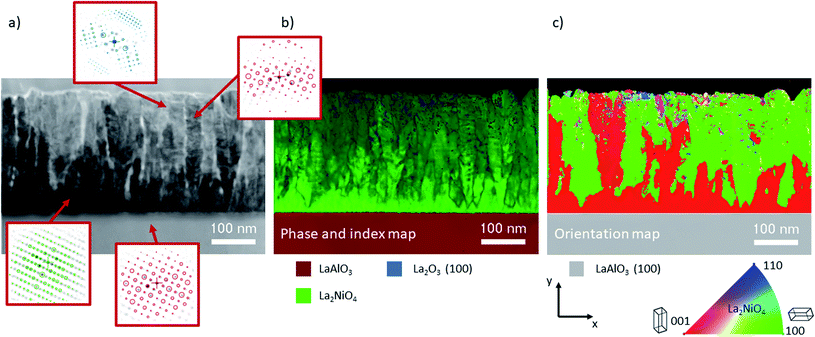
Phase and orientation of derived thin films are characterised by X-ray diffraction (XRD) in the θ–2θ configuration using a Bruker D8 Advance series II diffractometer (CuKα radiation). The surface homogeneity was studied using an FEG Gemini SEM 500 microscope in secondary (inlens) and backscattered electron mode with an accelerating voltage of 3 kV in high vacuum. Post image analysis was supported by the deep learning feature of MIPAR software. The surface morphology was further investigated by atomic force microscopy (AFM) in tapping mode using a Bruker Icon high performance AFM. Film thickness was obtained via X-ray reflectometry and transmission electron microscopy (TEM) analysis.L2NO4/LAO specimens were prepared in cross-sections using the semi-automated polishing tripod technique with a MultiPrep™ system (Allied High Tech Products, Inc.). A PIPS II from GATAN was used for the final polishing. TEM and high resolution TEM (HRTEM) images were recorded with a JEOL JEM 2010 LaB6 microscope operating at 200 kV with a 0.19 nm point-to-point resolution. The local structural properties of L2NO4/LAO films were further investigated by using an automated crystal phase and orientation mapping (ACOM) with a precession system (ASTAR) implemented in a JEOL 2100F FEG microscope. The crystal phase and orientation maps were obtained by precession of the primary electron beam around the microscope's optical axis at an angle of 1.2° while collecting the electron diffraction patterns at a rate of 100 frames per second with a step size of 2 nm. In this technique, the incident electron beam was a few nanometers in size and was precessed to reduce the dynamic effects and to enhance the indexing quality. The electron beam was simultaneously scanned over the area of interest to record an electron diffraction pattern at each location. For each point the local experimental electron diffraction patterns were compared with the complete set of theoretical diffraction patterns, which were computed for every expected crystalline phase and for a large number of orientations. The best match between the experimental and theoretical electron diffraction patterns permitted identification of both crystalline phase and orientation with a high precision. The crystal structures used for identification included La2NiO4, LaNiO3, La2O3 (cubic and hexagonal) and LaAlO3. Reliability is expressed by the lightness value in the index map, e.g. bright corresponds to high certainty.
Functional analysis
Functional properties were studied by electrical conductivity, electrical conductivity relaxation (ECR) and electrochemical impedance spectroscopy (EIS) measurements. For ECR measurements, samples were cut with a water cooled diamond saw into pieces of 5 × 5 mm. Electrical contacts were fabricated in the corners using Ag paint. For in situ characterisation, the samples were placed onto a 1/2′′ ceramic heating stage in a high temperature cell (Nextron). The surface temperature of the heater was calibrated beforehand using a Pt100 thermocouple and is assumed to be equivalent to the thin film temperature. The cell is equipped with electrical probes which are mechanically pinned onto the Ag electrodes and the electrical conductivity is measured in the Van-der-Pauw configuration using a small excitation current of 100 μA and 1 μA for L2NO4/(LAO or STO) and L2NO4/YSZ, respectively. The sample is annealed in a dynamic, dry, mixed O2/N2 atmosphere at 1 atm and a constant flow rate of 1000 ml min−1, whereas the oxygen partial pressure is controlled via the flow ratio of highly pure oxygen to nitrogen.This high gas flow is used to minimise the chamber flush time, which is about 4.5 s, as measured via the change of pO2 at the exit of the chamber using a Rapidox 2100 gas analyser. Temperature, pO2 and conductivity are automatically controlled and continuously recorded using Labview. The evolution of the conductivity is followed during isothermal annealing as a function of consecutive steps in pO2 between 210 and 10 mbar in the temperature range between 275 and 450 °C. The commonly used solution to Fick's second law of diffusion for a thin film with a linear surface exchange is applied and the proportionality between the transients of conductivity, σ and oxygen concentration, c, is assumed. One obtains:51
 | (1) |
 | (2) |
 | (3) |
 | (4) |
| τ = V/A/kchemδ | (5) |
 | (6) |
| τeff = aτ1 + (1 − a)τ2 | (7) |
In the mixed and diffusion limited regime, Ai ≠ 0 for all i. However, the value of Ai strongly decreases with increasing index, allowing one to focus on the first two time constants, having the highest values. For t → ∞ the normalised oxygen concentration of the solely diffusion limited process can be approximated by a single exponential decay54 with τ1 = 4d2/(π2Dchem) and A1 = 8/π2.
Electrochemical impedance spectroscopy (EIS) of nano-columnar L2NO4/YSZ (10 × 10 mm2) was carried out in dry air, between 450 and 650 °C, in the frequency range from 1 MHz to 1 Hz with an AC voltage of 50 mV and an active surface area of 8 × 8 mm2. Samples were studied in half-cell geometry with a painted, porous Au layer on top of the L2NO4 film and a painted, porous Ag layer on the back of the YSZ, serving as a current collector and low impedance counter-electrode, respectively.
Finite element method (FEM) simulations and sample geometry
FEM simulations are performed to analyse the thickness dependence of the exchange time constants for different sample geometries using COMSOL 5.5 on a 3D model of a single nano-column. A schematic is shown in Fig. 4. Based on this model, the specific surface area, being the actual exposed surface per in-plane surface, is estimated: | (8) |
Oxygen exchange takes place at the top and lateral surfaces of the nano-columns, with kchemδ as obtained for the dense L2NO4/YSZ film. The diffusion coefficient is assumed constant but anisotropic with Dchem,ab = 100Dchem,c.42 Time constants of the exchange process are obtained via fitting of the average oxygen concentration of the dense bottom layer as a function of time using one (surface limited regime) or two (diffusion limited process) exponential decays.
Results
Microstructure
The orientation and microstructure of L2NO4 thin films for different thicknesses are analysed by XRD using ICDD reference 04-015-2147, as shown in Fig. 1 for L2NO4/LAO (red curves). XRD patterns of all studied films (4 different thicknesses for each of the 3 studied substrates) can be found in ESI-Fig. 1.‡ Samples deposited on LAO and STO both show preferential growth along the c-axis (strong (00l) reflections) due to the small mismatch between the tetragonal L2NO4 in-plane cell parameter (3.868 Å) and the cubic unit cell of the substrate (3.791 Å and 3.905 Å, respectively), with minor contributions from the L2NO4 (103) and (110) orientations. However, with increasing thickness a contribution along the (200) direction arises, as exemplarily represented for L2NO4/LAO. For the thickest films, comparing the XRD peak areas of the (200) and (00l) reflections, the overall ab fraction within this film is estimated to be about 20%. This is caused by a loss of epitaxial growth with increasing film thickness, as was previously reported for L2NO4/STO thin films deposited by PLD.55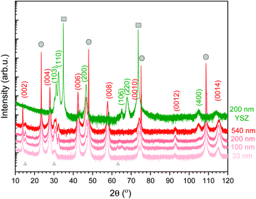 | ||
| Fig. 1 XRD pattern of L2NO4 thin films of various thicknesses deposited at 650 °C on LAO (red curves). Additionally, the 200 nm L2NO4/YSZ sample is shown (green), while XRD data for all thicknesses on all substrates are compared in ESI-Fig. 1.‡ Substrate peaks are marked by grey circles (LAO) and squares (YSZ). The observed L2NO4 planes are labelled according to ICDD reference 04-015-2147. Films on LAO possess a preferential growth direction along the (001) direction. With increasing thickness, an additional orientation along the (100) direction is detected. For L2NO4/YSZ, polycrystalline growth preferentially-oriented along the (110), (100) and (103) direction is observed. Small amounts of excess La are present in the film, leading to the formation of La2O3 (grey triangles, ICDD reference 01-071-5408). | ||
The La/Ni ratio in the precursor solution was fixed at 5, while the solution-to-layer transfer ratio depends on the deposition temperature. For films deposited at 650 °C, the final La/Ni ratio in the film was quantified by electron micro probe analysis and was found to be 2.5. This excess of La is observed via the presence of the La2O3 phase in XRD spectra (2θ peaks at around 14, 30 and 63°, marked with grey triangles in Fig. 1).
Polycrystalline growth with preferential orientation along the (110), (100) and (103) direction is observed for films deposited on YSZ with a cell parameter of 5.144 Å, also shown in Fig. 1 (green diffraction pattern). The two epitaxial and the preferentially oriented polycrystalline systems allow us to study the influence of orientation on exchange kinetics.
Epitaxial growth on LAO or STO introduces tensile or compressive strain, respectively, in very thin layers. However, the c-axis lattice parameter of the as-deposited L2NO4 films, calculated via the Nelson–Riley formula, does not reveal a substrate dependent thickness dependence (between 33 and 540 nm), see ESI-Fig. 2.‡ Therefore, we assume that any substrate induced strain is released by the formation of extended structural defects, already for the thinnest films studied.
The L2NO4/LAO and L2NO4/STO samples deposited at 650 °C consist of homogeneous, square and rectangular shaped grains as observed by SEM analysis, Fig. 2. With increasing thickness the structure evolves from a dense layer to a columnar one, with the individual grains becoming vertically separated. This is expected to lead to an increase of the specific surface area and the surface to volume ratio (SVR). Additionally, the apparent average grain size increases, while the grain size distributions becomes broader (ESI-Fig. 3‡). In agreement with the structure zone model, the formation of the columnar structure can be prevented by increasing the deposition temperature, e.g. a 200 nm thick film deposited at 750 °C possesses a dense surface, see ESI-Fig. 4.‡ L2NO4 thin films grown on YSZ single crystal substrates show the same tendency of increasing grain size and evolution towards separated columns with thickness, but the grain shape does not show the same rectangular features. The surface morphology from AFM imaging shows increasing roughness with increasing film thickness, ESI-Fig. 5.‡
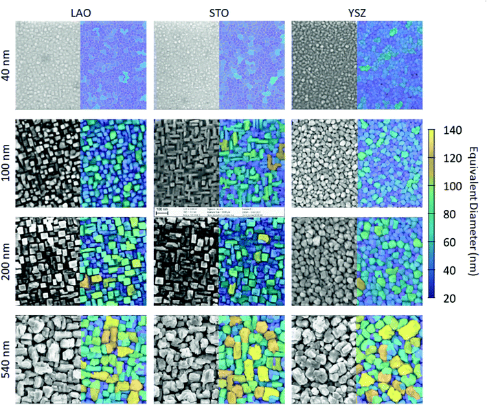 | ||
| Fig. 2 Surface morphology of L2NO4 thin films: SEM analysis of L2NO4 films of different thicknesses deposited on top of LAO, STO and YSZ single crystals at 650 °C. False colour indicates the grain size using the equivalent diameter of a circular grain of the same area. Corresponding histograms are shown in ESI-Fig. 3.‡ | ||
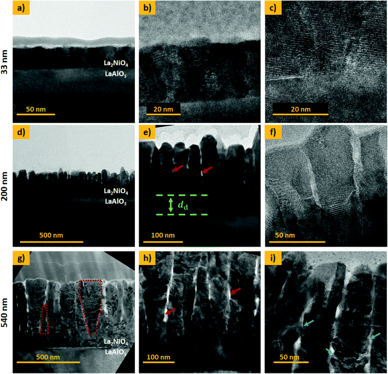
Cross-section TEM analysis of the 33 nm thick film is shown in the top panel of Fig. 3(a–c). The structure consists of closed packed columnar grains and a smooth, flat surface. The 200 and 540 nm thick films, shown in Fig. 3(d–f) and (g–i), respectively, display a different microstructure featuring two distinct zones, namely a dense interfacial layer on top of the substrate, followed by a nano-columnar structure. The thickness of the dense bottom layer, dd, shows some local variation with an average thickness of approximately 80 and 100 nm, respectively. Such a dense layer was described previously and seems to be a common feature for the growth of oxides by physical and chemical vapour deposition techniques.29 In μSOCs it is expected that this dense layer serves as an out-of-plane oxygen diffusion and in-plane electronic (holes) conduction pathway, with good adherence to the electrolyte. The grains in the columnar top region are vertically gapped by a few nanometres and cavities or nano-pores are present in the material, in which the gas is expected to enter (red arrows in Fig. 3(e) and (h)). For the 540 nm thick sample, V-shaped grains can be found, as exemplarily marked for one of the grains in Fig. 3(g), which is characteristic of zone T type growth. Additionally for the thickest film, a high density of kinks and edges is found on the lateral surface of the nano-columns, marked with blue arrows in Fig. 3(i). These regions are potential hosts to highly active sites, as surface electronic states are thought to be significantly varied in proximity to these defects. STEM EDX images are displayed in ESI-Fig. 6,‡ exemplarily for the 540 nm thick L2NO4/LAO sample, showing a homogeneous La and Ni distribution throughout the film.
Based on our TEM observations, we designed a simplified geometric model shown in Fig. 4, similar to the one developed initially by Plonczak et al.29 This model was used for the COMSOL simulations and for the estimation of the thickness dependence of the specific surface area. The parameters used to model each of the films, such as thickness, grain size and dense layer thickness are obtained by SEM and TEM observations and are summarised in Table 1.
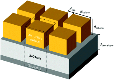 | ||
| Fig. 4 Simple geometric model for finite element (COMSOL) simulations to study the influence of geometrical parameters on oxygen exchange activity and estimate the exposed surface area. | ||
| Total film thickness (nm) | Grain size (nm) | Thickness dense layer (nm) | SVR (μm−1) |
|---|---|---|---|
| 33 | 28 ± 8 | 33 | 30 |
| 100 | 46 ± 12 | 60* | 44 |
| 200 | 50 ± 18 | 80 ± 20 | 52 |
| 540 | 55 ± 27 | 100 ± 20 | 61 |
Automated crystal phase and orientation mapping in TEM (ASTAR) has been used to further study the film microstructure on a nanoscale, as shown in Fig. 5. As already shown by XRD, La2NiO4 is the dominant phase across the whole film thickness. Only in the upper half, a small quantity of impurities in the form of La2O3 inclusions could potentially be present (low reliability index). Ambiguity, and hence low reliability, in near surface regions is likely caused by the superposition of several small grains within the thickness of the TEM lamella. The orientation map shows a thin c-axis oriented interfacial layer on top of the substrate. This epitaxial layer is in some regions limited to about 10 nm, followed by (100) oriented L2NO4, which in the observed region makes up more than 50% of the thin film volume.
The microstructural stability of the electrode material was evaluated after the films' functional characterisation by XRD and SEM, as shown exemplarily for the 200 nm thick L2NO4/LAO sample in ESI-Fig. 7.‡ Within the studied temperature, temporal and atmospheric conditions (e.g. up to 550 °C and 24 h at elevated temperature in a dry atmosphere at 1 atm, with a pO2 between 10 mbar and 210 mbar), no microstructural evolution was observed, i.e. no formation of new phases was detected by XRD, and no grain growth, segregation or significant morphological surface changes were found by SEM.
Functional properties
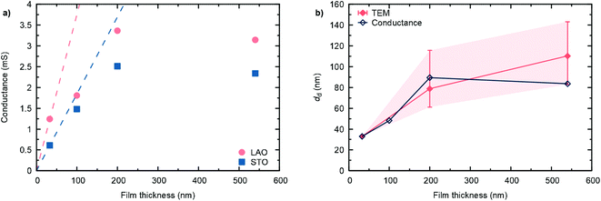
The high temperature in-plane conductance (Van-der-Pauw) increases with increasing film thickness, as shown for the different samples in Fig. 6(a). While in the dense, 33 nm thick film the full sample volume contributes to the observed conductance, in the thicker, nano-columnar structured layers only the dense, bottom part of the cross section is active in the current percolation. Hence, for d > 33 nm, the measured conductance falls below the extrapolated conductance from the thinnest sample. As a first approximation, assuming constant conductivity throughout the whole sample thicknesses (neglecting effects from oxygen stoichiometry and other kinds of defects), we can estimate an average thickness of the dense, conduction pathway, as shown in Fig. 6(b). Values are in reasonable agreement with TEM observations, where some local differences were found.
 | (9) |
 | (10) |
 and
and  being the oxygen interstitial and its vacancy, respectively, and h˙ an electron hole in the valence band. Factors governing the ORR are (i) temperature, (ii) the surface exchange coefficient, kchemδ, (iii) the chemical diffusion coefficient, Dchem, (iv) the (electro-) chemical driving force, e.g. the oxygen chemical potential difference, ΔμO, between the initial state and final equilibrium, (v) the surface area, where the reaction takes place, and (vi) the sample volume, which defines the amount of oxygen ions which need to pass through the surface to compensate ΔμO.
The normalised conductivity transients of L2NO4 thin films at 375 °C after a change of pO2 from 10–250 mbar are shown in ESI-Fig. 8‡ and eqn (6) was used to fit experimental data. The effective oxidation time constants are shown in an Arrhenius plot in Fig. 7 for nano-columnar films of various thicknesses deposited at 650 °C. Additionally, a dense 200 nm thick L2NO4/YSZ sample, deposited at 750 °C, is depicted. For all samples, thermal activation is observed, with shorter time constants at higher temperatures. For thick L2NO4 films on YSZ at high temperatures, the obtained time constants might be slightly affected by the chamber flush time, and therefore correspond to an upper limit (their real value could potentially be even lower). However, as these values follow well an Arrhenius type behaviour, they can be considered reliable.
By extrapolation of reported chemical diffusion coefficients (from ECR measurements) for L2NO4 at high temperatures to 400 °C, a Dchem in the range of 7 × 10⁻⁸ cm2 s−1 to 5 × 10⁻⁶ cm2 s−1 can be estimated.57,60,61 The critical thickness, where surface exchange and diffusion become equally important, is thus in the order of millimetres (tc = Dchem/kchemδ with kchemδ ≈ 1 × 10⁻⁶ cm s−1, see below). It is therefore plausible to further analyse the time constants of the studied thin films with respect to a surface limited process.
Apparent activation energies, EA, calculated for the oxidation surface exchange coefficient (kchemδ ∝ 1/τ1), decrease from 1.3 ± 0.2 eV for the dense films to about 1 ± 0.2 eV for columnar structured samples and are similar to previously reported values for La2NiO4.38,59 However, we note that reported activation energies range from 0.4 to 1.9 eV for single crystals, pellets and thin films with different terminations.39,61,62
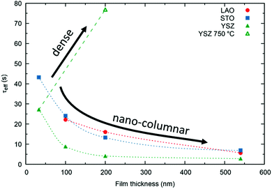
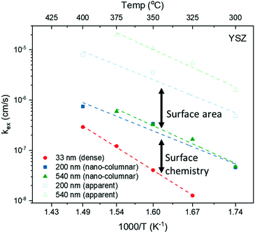
We stress the fact that for the nano-columnar layers deposited at 650 °C, saturation times drastically decrease with increasing film thickness, as shown for one temperature (T = 375 °C) in Fig. 8. Independent of the substrate, saturation times are one order of magnitude shorter for the thickest films as compared to the dense 33 nm thick ones. A similar, but much weaker dependence of saturation times on thickness was observed previously in L2NO4 thin films and was ascribed to the increased roughness in thicker films.39 On the other hand, as expected, the dense 200 nm thick L2NO4/YSZ sample, deposited at 750 °C, exhibits a higher time constant.
Preliminary electrochemical impedance spectroscopy (EIS) results for nano-columnar structured 100 and 200 nm thick L2NO4/YSZ films confirm the enhanced activity in thicker films, as shown in ESI-Fig. 9.‡ The area specific resistance (ASR) of the 200 nm thick L2NO4 layer was found to be about a factor of 2 smaller than the ASR of the 100 nm thick film, well in agreement with the enhancement obtained by ECR measurements (compare with Fig. 8). Both techniques reveal an activation energy of about 1.1 eV independent of film thickness.
When comparing films grown on LAO and STO with YSZ, one can evaluate the influence of orientation on the exchange activity.
While films on LAO and STO exhibit similar saturation times, samples grown on YSZ have shorter time constants. The thickness and substrate dependence will be discussed in the following.
Discussion
To get a better understanding of the influence of the different microstructures on the oxygen exchange kinetics, COMSOL simulations have been performed using the model shown in Fig. 4, with the geometric model parameters given in Table 1.We have studied four different scenarios: two microstructures (dense and nano-columnar) under surface limitation, as prevailing in our thin films (see above) and within the diffusion limited regime, for the sake of completeness.
The resulting thickness dependences of saturation times, corresponding to values obtained from ECR measurements, are shown in Fig. 9 and compared to the ones found experimentally for L2NO4/YSZ.
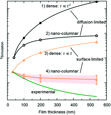 | ||
| Fig. 9 Expected thickness dependence of the saturation time, τ (as obtained from ECR measurements) for dense (open symbols) and nano-columnar (filled symbols) thin film structures for the surface (triangles) and diffusion limited (circles) regime, obtained from finite element simulations. Model description and parameters, used for the simulations, are given in the main text and Table 1 and correspond to experimentally observed values. Scenario (4), regarding the nano-columnar structured, surface limited case, strongly depends on the grain size and its evolution with thickness. The green line corresponds to the experimentally obtained thickness dependence for L2NO4/YSZ (data from Fig. 8). | ||
(1) Diffusion limited, dense film
If the Biot number is sufficiently large (Bi = tkchemδ/Dchem > 30), the exchange process is diffusion limited51 and saturation times are approximately proportional to the square of the thickness.(2) Diffusion limited, nano-columnar structure
Also for this case FEM simulations reveal an increase of saturation times with thickness, however, a much weaker dependence is obtained as compared to the dense, diffusion limited scenario.(3) Surface limited, dense layer
This is the only case with an exact analytic solution, where the saturation time increases linearly with film thickness, τ = d/(kchemδ).(4) Surface limited, nano-columnar structure
This scenario strongly depends on the geometric model. In the realm of surface limitation, τ is inversely proportional to the surface to volume ratio: τ = (V/A)/(kchemδ). Hence, the introduction of surface roughness or open porosity can have a drastic impact on measured saturation times, as can be clearly seen for case 4 in Fig. 9, being the only situation where the time constant is expected to decrease with thickness, as experimentally found for the studied thin films (see also Fig. 8). In the presence of nano-columns, the active surface area is strongly enlarged, consequently increasing the total oxygen ion flux through the surface. This result shows the potential of nano-tailoring surfaces and morphologies to enhance the apparent oxygen exchange activity of electrode materials. In the present model, grain size and its evolution with thickness firmly affect the surface to volume ratio, while the width of the gap between two grains has a minor influence. Simulations were performed using the grain size distribution obtained by SEM analysis. However, the enlarged surface alone cannot fully account for the strong decrease of the time constant with thickness found experimentally, which is discussed in the following.The influence of nano-columnar growth on the surface exchange coefficient, kex, calculated using eqn (5) and the SVRs given in Table 1, is depicted in Fig. 10. Exchange coefficients for the nano-columnar films are significantly faster than the ones of the dense sample. We suggest that the enhancement of intrinsic activity is due to the exposure of additional crystal orientations and associated changes in surface termination and surface chemistry, and possibly highly active nano-features such as kinks and edges being numerously present within the lateral surface.
The gain of activity related to the enlarged surface area can be depicted using the apparent exchange coefficient, equivalent to the surface exchange coefficient required for a dense layer (of the same thickness) to exchange oxygen as fast as a nano-columnar one.
With this in mind, one can return to the differences found in Fig. 7(b), between films of different orientations. While films on LAO and STO exhibit preferential c-axis growth (001), particularly for the thinnest films, L2NO4 layers on YSZ grow mainly along the (110) and (100) direction. From previous experimental and theoretical results it is known that the (100) terminated surface has higher intrinsic activity42,45 as compared to the (001) orientation. This can explain the shorter time constants obtained for L2NO4/YSZ with respect to films on LAO and STO. Taking into account that with increasing film thickness also films on LAO and STO show an increasing presence of the (100) orientation, it is expected that this contributes to the faster oxygen exchange in these films.
Another potentially influencing factor, currently being investigated within our group, is the amount of Ni present directly in the top surface layers. A-site (La, Sr) cation domination was found in several perovskite-based, dense oxides,63 and in particular in (La,Sr)2NiO4 single crystals with cleaved surfaces47 and in bulk La2NiO4.63 However, the La and Ni cation distribution could be strongly affected by the nano-columnar structure with its small grain size, with implications on the surface chemistry of the material, which is yet to be confirmed.
Conclusions
In this work we have demonstrated how to tune the apparent and intrinsic activity of La2NiO4 thin films by tailoring its nano-structure. Samples were synthesized by PI-MOCVD on different single crystal substrates with thickness ranging between 33 and 540 nm. We were able to tune the morphology of the films by varying the deposition temperature (650–750 °C) in agreement with the structure zone model, to achieve a nano-columnar microstructure with open porosity and significantly enlarged specific surface area at lower deposition temperatures. ECR measurements revealed remarkably enhanced surface activity in thicker, nano-architectured films, as compared to thin, dense ones. While the larger surface area plays an important role, it does not account for the total activity increase. Hence, apparent as well as intrinsic activity was improved. We concluded that the latter was enhanced by changes in the grain orientation and the exposed surfaces with distinct, faster exchange coefficients, while additional features on the lateral side of the nano-columns such as kinks and edges are thought to also improve oxygen exchange, as these defects are expected to strongly modify surface electronic states involved in the reaction mechanism. Overall, the nano-columnar growth of L2NO4 by PI-MOCVD resulted in a substantial enhancement of the oxygen exchange activity and opens up a new route towards the optimisation of electrode materials for intermediate to low temperature μSOC devices.Data availability
All sample datasets and materials related to this work are made available under CC BY 4.0 license in the zenodo repository: 10.5281/zenodo.5564457.Author contributions
Conceptualization: MB, AS; investigation: AR, AS, LR, JMC, JS, FB; formal analysis: AR, AS, LR; methodology: AS, AR, CJ, MB; writing – original draft: AS; writing – review & editing: AS, MB, AR, CJ, MM, AT.Conflicts of interest
There are no conflicts to declare.Acknowledgements
This work has received funding from the European Union's Horizon 2020 research and innovation program under grant agreement no. 824072 (Harvestore) and under the Marie Skłodowska-Curie grant agreement no. 840787 (Thin-CATALYzER). The authors further acknowledge financial, scientific and technical support from CNRS, Grenoble INP, UGA and the scientific and technical assistance of Gilles Renou for ASTAR technique of the CMTC characterization platform of Grenoble INP, which is supported by the Centre of Excellence of Multifunctional Architectured Materials (LabEx CEMAM).References
- H. J. M. Bouwmeester, H. Kruidhof and A. J. Burggraaf, Importance of the surface exchange kinetics as rate limiting step in oxygen permeation through mixed-conducting oxides, Solid State Ionics, 1994, 72, 185–194 CrossRef CAS.
- Z. Gao, L. V. Mogni, E. C. Miller, J. G. Railsback and S. A. Barnett, A perspective on low-temperature solid oxide fuel cells, Energy Environ. Sci., 2016, 9, 1602–1644 RSC.
- Z. Li, M. Li and Z. Zhu, Perovskite Cathode Materials for Low-Temperature Solid Oxide Fuel Cells: Fundamentals to Optimization, Electrochem. Energy Rev., 2021 DOI:10.1007/s41918-021-00098-3.
- C. Sun, J. A. Alonso and J. Bian, Recent Advances in Perovskite-Type Oxides for Energy Conversion and Storage Applications, Adv. Energy Mater., 2021, 11, 2000459 CrossRef CAS.
- A. Stangl, D. Muñoz-Rojas and M. Burriel, In situ and operando characterisation techniques for solid oxide electrochemical cells: Recent advances, JPhys Energy, 2021, 3, 012001 CrossRef CAS.
- F. Baiutti, et al., Direct Measurement of Oxygen Mass Transport at the Nanoscale, Adv. Mater., 2021, 2105622, DOI:10.1002/adma.202105622.
- G. Yang, et al., Toward reducing the operation temperature of solid oxide fuel cells: Our past 15 years of efforts in cathode development, Energy Fuels, 2020, 34, 15169–15194 CrossRef CAS.
- J. Yoon, et al., Vertically aligned nanocomposite thin films as a cathode/electrolyte interface layer for thin-film solid oxide fuel cells, Adv. Funct. Mater., 2009, 19, 3868–3873 CrossRef CAS.
- M. Acosta, F. Baiutti, A. Tarancón and J. L. MacManus-Driscoll, Nanostructured Materials and Interfaces for Advanced Ionic Electronic Conducting Oxides, Adv. Mater. Interfaces, 2019, 6, 1900462 CrossRef.
- J. S. A. Carneiro, R. A. Brocca, M. L. R. S. Lucena and E. Nikolla, Optimizing cathode materials for intermediate-temperature solid oxide fuel cells (SOFCs): Oxygen reduction on nanostructured lanthanum nickelate oxides, Appl. Catal., B, 2017, 200, 106–113 CrossRef CAS.
- K. Boulahya, D. Muñoz-Gil, A. Gómez-Herrero, M. T. Azcondo and U. Amador, Eu2SrCo1.5Fe0.5O7 a new promising Ruddlesden-Popper member as a cathode component for intermediate temperature solid oxide fuel cells, J. Mater. Chem. A, 2019, 7, 5601–5611 RSC.
- D. Lee, et al., Strontium influence on the oxygen electrocatalysis of La2−xSrxNiO4±δ (0.0 ≤ x Sr ≤ 1.0) thin films, J. Mater. Chem. A, 2014, 2, 6480–6487 RSC.
- M. Sase, et al., Enhancement of oxygen exchange at the hetero interface of (La,Sr)CoO3/(La,Sr)2CoO4 in composite ceramics, Solid State Ionics, 2008, 178, 1843–1852 CrossRef CAS.
- J. W. Han and B. Yildiz, Mechanism for enhanced oxygen reduction kinetics at the (La,Sr)CoO3−δ/(La,Sr)2CoO4+δ hetero-interface, Energy Environ. Sci., 2012, 5, 8598–8607 RSC.
- J. Hwang, et al., Tuning perovskite oxides by strain: Electronic structure, properties, and functions in (electro)catalysis and ferroelectricity, Mater. Today, 2019, 31, 100–118 CrossRef CAS.
- D. Lee, et al., Stretching Epitaxial La0.6Sr0.4CoO3−δ for Fast Oxygen Reduction, J. Phys. Chem. C, 2017, 121, 25651–25658 CrossRef CAS.
- A. M. Saranya, et al., Engineering Mixed Ionic Electronic Conduction in La0.8Sr0.2MnO3+δ Nanostructures through Fast Grain Boundary Oxygen Diffusivity, Adv. Energy Mater., 2015, 5, 1500377 CrossRef.
- H. L. Tuller and S. R. Bishop, Point defects in oxides: Tailoring materials through defect engineering, Annu. Rev. Mater. Res., 2011, 41, 369–398 CrossRef CAS.
- M. Choi, et al., Engineering of Charged Defects at Perovskite Oxide Surfaces for Exceptionally Stable Solid Oxide Fuel Cell Electrodes, ACS Appl. Mater. Interfaces, 2020, 12, 21494–21504 CrossRef CAS PubMed.
- M. Ghamarinia, A. Babaei and C. Zamani, Electrochemical characterization of La2NiO4-infiltrated La0.6Sr0.4Co0.2Fe0.8O3−δ by analysis of distribution of relaxation times, Electrochim. Acta, 2020, 353, 1–9 CrossRef.
- J. M. Vohs and R. J. Gorte, High-performance SOFC cathodes prepared by infiltration, Adv. Mater., 2009, 21, 943–956 CrossRef CAS.
- G. Yang, S.-Y. Kim, C. Sohn, J. K. Keum and D. Lee, Influence of Heterointerfaces on the Kinetics of Oxygen Surface Exchange on Epitaxial La1.85Sr0.15CuO4 Thin Films, Appl. Sci., 2021, 11, 3778 CrossRef CAS.
- Y. Y. Chen, et al., A robust and active hybrid catalyst for facile oxygen reduction in solid oxide fuel cells, Energy Environ. Sci., 2017, 10, 964–971 RSC.
- M. L. Weber, et al., Exsolution of Embedded Nanoparticles in Defect Engineered Perovskite Layers, ACS Nano, 2021, 15, 4546–4560 CrossRef CAS PubMed.
- Y. H. Lee, et al., All-Sputtered, Superior Power Density Thin-Film Solid Oxide Fuel Cells with a Novel Nanofibrous Ceramic Cathode, Nano Lett., 2020, 20, 2943–2949 CrossRef CAS PubMed.
- W. Zhang, et al., La0.6Sr0.4Co0.2Fe0.8O3−δ/CeO2 Heterostructured Composite Nanofibers as a Highly Active and Robust Cathode Catalyst for Solid Oxide Fuel Cells, ACS Appl. Mater. Interfaces, 2019, 11, 26830–26841 CrossRef CAS PubMed.
- M. P. Wells, et al., Route to High-Performance Micro-solid Oxide Fuel Cells on Metallic Substrates, ACS Appl. Mater. Interfaces, 2021, 13, 4117–4125 CrossRef CAS PubMed.
- L. Almar, et al., High-surface-area ordered mesoporous oxides for continuous operation in high temperature energy applications, J. Mater. Chem. A, 2014, 2, 3134–3141 RSC.
- P. Plonczak, et al., Tailoring of LaxSr1−xCoyFe1−yO3−δ nanostructure by pulsed laser deposition, Adv. Funct. Mater., 2011, 21, 2764–2775 CrossRef CAS.
- J. A. Thornton, High Rate Thick Film Growth, Annu. Rev. Mater. Sci., 1977, 7, 239–260 CrossRef CAS.
- P. B. Barna and M. Adamik, Fundamental structure forming phenomena of polycrystalline films and the structure zone models, Thin Solid Films, 1998, 317, 27–33 CrossRef CAS.
- N. Kaiser, Review of the fundamentals of thin-film growth, Appl. Opt., 2002, 41, 3053 CrossRef CAS PubMed.
- V. A. Shchukin and D. Bimberg, Spontaneous ordering of nanostructures on crystal surfaces, Rev. Mod. Phys., 1999, 71, 1125–1171 CrossRef CAS.
- M. Mosleh, M. Søgaard and P. V. Hendriksen, Kinetics and Mechanisms of Oxygen Surface Exchange on La0.6Sr0.4FeO3−δ Thin Films, J. Electrochem. Soc., 2009, 156, B441 CrossRef CAS.
- M. Søgaard, A. Bieberle-Hütter, P. V. Hendriksen, M. Mogensen and H. L. Tuller, Oxygen incorporation in porous thin films of strontium doped lanthanum ferrite, J. Electroceram., 2011, 27, 134–142 CrossRef.
- P. Plonczak, M. Søgaard, A. Bieberle-Hütter, P. V. Hendriksen and L. J. Gauckler, Electrochemical Characterization of La0.58Sr0.4Co0.2Fe0.8O3−δ Thin Film Electrodes Prepared by Pulsed Laser Deposition, J. Electrochem. Soc., 2012, 159, B471–B482 CrossRef CAS.
- G. Kim, S. Wang, A. J. Jacobson and C. L. Chen, Measurement of oxygen transport kinetics in epitaxial La2NiO4+δ thin films by electrical conductivity relaxation, Solid State Ionics, 2006, 177, 1461–1467 CrossRef CAS.
- W. Li, et al., New mechanistic insight into the oxygen reduction reaction on Ruddlesden-Popper cathodes for intermediate-temperature solid oxide fuel cells, Phys. Chem. Chem. Phys., 2016, 18, 8502–8511 RSC.
- G. Garcia, M. Burriel, N. Bonanos and J. Santiso, Electrical Conductivity and Oxygen Exchange Kinetics of La2NiO4+δ Thin Films Grown by Chemical Vapor Deposition, J. Electrochem. Soc., 2008, 155, P28 CrossRef CAS.
- R. Moreno, et al., Chemical Strain Kinetics Induced by Oxygen Surface Exchange in Epitaxial Films Explored by Time-Resolved X-ray Diffraction, Chem. Mater., 2013, 25, 3640–3647 CrossRef CAS.
- J. M. Bassat, P. Odier, A. Villesuzanne, C. Marin and M. Pouchard, Anisotropic ionic transport properties in La2NiO4+δ single crystals, Solid State Ionics, 2004, 167, 341–347 CrossRef CAS.
- M. Burriel, et al., Anisotropic oxygen diffusion properties in epitaxial thin films of La2NiO4+δ, J. Mater. Chem., 2008, 18, 416–422 RSC.
- M. Burriel, et al., Influence of Crystal Orientation and Annealing on the Oxygen Diffusion and Surface Exchange of La2NiO4+δ, J. Phys. Chem. C, 2016, 120, 17927–17938 CrossRef CAS.
- J. M. Bassat, et al., Anisotropic oxygen diffusion properties in Pr2NiO4+δ and Nd2NiO4+δ single crystals, J. Phys. Chem. C, 2013, 117, 26466–26472 CrossRef CAS.
- X. Ma, et al., Engineering Complex, Layered Metal Oxides: High-Performance Nickelate Oxide Nanostructures for Oxygen Exchange and Reduction, ACS Catal., 2015, 5, 4013–4019 CrossRef CAS.
- X. K. Gu and E. Nikolla, Design of Ruddlesden-Popper Oxides with Optimal Surface Oxygen Exchange Properties for Oxygen Reduction and Evolution, ACS Catal., 2017, 7, 5912–5920 CrossRef CAS.
- M. Burriel, et al., Absence of Ni on the outer surface of Sr doped La2NiO4 single crystals, Energy Environ. Sci., 2014, 7, 311–316 RSC.
- J. Wu, S. S. Pramana, S. J. Skinner, J. A. Kilner and A. P. Horsfield, Why Ni is absent from the surface of La2NiO4+δ?, J. Mater. Chem. A, 2015, 3, 23760–23767 RSC.
- R. Gao, et al., Correlating Surface Crystal Orientation and Gas Kinetics in Perovskite Oxide Electrodes, Adv. Mater., 2021, 33, 2100977 CrossRef CAS PubMed.
- D. Lee, et al., Strain influence on the oxygen electrocatalysis of the (100)-oriented epitaxial La2NiO4+δ thin films at elevated temperatures, J. Phys. Chem. C, 2013, 117, 18789–18795 CrossRef CAS.
- M. W. den Otter, H. J. M. Bouwmeester, B. A. Boukamp and H. Verweij, Reactor Flush Time Correction in Relaxation Experiments, J. Electrochem. Soc., 2001, 148, J1 CrossRef CAS.
- L. Chen, C. L. Chen and A. J. Jacobson, Electrical Conductivity Relaxation Studies of Oxygen Transport in Epitaxial YBa2Cu3O7−δ Thin Films, IEEE Trans. Appl. Supercond., 2003, 13, 2882–2885 CrossRef CAS.
- L. Yan, B. Kavaipatti, K.-C. Chang, H. You and P. Salvador, Microstructural Effects on the Oxygen Exchange Kinetics of La0.7Sr0.3MnO3 Thin Films, ECS Trans., 2019, 35, 2063–2075 CrossRef.
- R. Merkle and J. Maier, How is oxygen incorporated into oxides? A comprehensive kinetic study of a simple solid-state reaction with SrTiO3 as a model material, Angew. Chem., Int. Ed., 2008, 47, 3874–3894 CrossRef CAS PubMed.
- D. Telesca, B. O. Wells and B. Sinkovic, Structural reorientation of PLD grown La2NiO4 thin films, Surf. Sci., 2012, 606, 865–871 CrossRef CAS.
- M. Burriel, et al., Enhancing Total Conductivity of La2NiO4+δ Epitaxial Thin Films by Reducing Thickness, J. Phys. Chem. C, 2008, 112, 10982–10987 CrossRef CAS.
- J. Song, D. Ning, B. Boukamp, J. M. Bassat and H. J. M. Bouwmeester, Structure, electrical conductivity and oxygen transport properties of Ruddlesden-Popper phases Ln: N + 1NinO3n +1(Ln = La, Pr and Nd; N = 1, 2 and 3), J. Mater. Chem. A, 2020, 8, 22206–22221 RSC.
- X. Tong, et al., Performance and stability of Ruddlesden-Popper La2NiO4+δ oxygen electrodes under solid oxide electrolysis cell operation conditions, Ceram. Int., 2017, 43, 10927–10933 CrossRef CAS.
- X. Li, et al., Defects evolution of Ca doped La2NiO4+δ and its impact on cathode performance in proton-conducting solid oxide fuel cells, Int. J. Hydrogen Energy, 2020, 45, 17736–17744 CrossRef CAS.
- Z. Li and R. Haugsrud, Effects of surface coatings on the determination of Dchem and kchem in La2NiO4+δ by conductivity relaxation, Solid State Ionics, 2012, 206, 67–71 CrossRef CAS.
- A. Egger and W. Sitte, Enhanced oxygen surface exchange of La2NiO4+δ by means of a thin surface layer of silver, Solid State Ionics, 2014, 258, 30–37 CrossRef CAS.
- M. V. Ananyev, et al., Oxygen isotope exchange in La2NiO4±δ, Phys. Chem. Chem. Phys., 2016, 18, 9102–9111 RSC.
- J. Druce, et al., Surface termination and subsurface restructuring of perovskite-based solid oxide electrode materials, Energy Environ. Sci., 2014, 7, 3593–3599 RSC.
Footnotes |
| † Mónica Burriel writes: John Kilner was my “scientific father” during the years I spent at Imperial College as a young scientist, undoubtedly a key period of my scientific career. John was a great mentor, who transmitted his personal enthusiasm and in-depth knowledge in Solid State Ionics in each scientific discussion, as he still does nowadays. It is thus a great honour for me to contribute to this special issue with an article focused on La2NiO4 thin films, somewhat the continuation and extension of our first joint work back in 2008, published in this same journal. |
| ‡ Electronic supplementary information (ESI) available. See DOI: 10.1039/d1ta09110g |
| This journal is © The Royal Society of Chemistry 2022 |

