
Nanostructured electroless Ni deposited SnO2 for solar hydrogen production†
Priyanka N.
Birla
 a,
Sudhir
Arbuj
a,
Ratna
Chauhan
b,
Manish
Shinde
a,
Sunit
Rane
a,
Suresh
Gosavi
b and
Bharat
Kale
*ac
a,
Sudhir
Arbuj
a,
Ratna
Chauhan
b,
Manish
Shinde
a,
Sunit
Rane
a,
Suresh
Gosavi
b and
Bharat
Kale
*ac
aCentre for Materials for Electronics Technology, Off Pashan Road, Panchwati, Pune-411008, India. E-mail: bbkale1@gmail.com
bDepartment of Environment Science, Savitribai Phule Pune University, Pune-411007, India
cMaterial Science Department, MITWPU, University Paud Road, Pune 38, India
First published on 27th August 2024
Abstract
Herein, Ni-decorated SnO2 (Ni@SnO2) nanostructures have been synthesized using SnO2 as a matrix via a simple electroless deposition method for the generation of hydrogen, a potent near-future fuel. XRD analysis confirmed the generation of rutile SnO2 in Ni@SnO2. FESEM and FETEM imaging exhibited the formation of SnO2 nanoparticles with a size of 10–50 nm, which are deposited with Ni nanoparticles (5–7 nm) and intermittent films (thickness 1–2 nm). The associated EDS elemental mapping validated Ni deposition on the surface of the SnO2 nanoparticles, further supplemented by FTIR, Raman and XPS analysis. Slight red shifts in the band gaps of the Ni@SnO2 nanostructures (in the range of 3.53–3.65 eV) compared to the pristine SnO2 nanoparticles (3.72 eV) were observed. Also, intensity quenching of the band gap and associated defect peaks were observed in PL analysis. The Ni@SnO2 nanostructures were used as photocatalysts and exhibited proficient hydrogen evolution. Among the samples, the 0.3 wt% Ni@SnO2 nanostructures showed the greatest hydrogen evolution, i.e., ∼50 μmol g−1 h−1 under visible light irradiation versus pristine SnO2 (8.5 μmol g−1 h−1) owing to the enhanced density of active sites and effective charge separation. It is noteworthy that the hydrogen evolution is much better as compared to earlier reports of Pt-doped-SnO2 based materials.
Introduction
Fuels play a vital role in the progressive industrialized economy, in which an enormous amount of energy is required for various processes such as heating, lighting, transportation, power generation, production, etc. Until the last few decades, the world relied heavily on fossil fuels. In the contemporary scenario, depletion of perishable energy sources as well as environmental issues such as global warming have arisen, and the world is facing an energy crisis that requires significant attention. Researchers are focusing on environmentally friendly concrete technologies for energy generation using various sustainable sources with assured energy security.When the various sustainable energy fuel options are scrutinized, hydrogen is found to be the apt alternative, although it is in its infancy in terms of development of the technology (hydrogen economy) owing to the bottlenecks related to its safe and efficient storage and delivery.1 Its vast energy capacity, as well as its relatively clean and energy-efficient nature, make hydrogen a proficient energy carrier.2 As 8% of overall energy demand is predicted to be fulfilled via hydrogen by the year 2050, a need for the development of hydrogen production methods with near-zero greenhouse gas emissions has arisen.3
At present, the overall demand of hydrogen is overwhelmingly (>95% of total demand) satisfied by the steam reforming process or the partial oxidation of hydrocarbons with the inevitable generation of carbon dioxide.4 As an alternative, water splitting is a relatively greener method of hydrogen production carried out using techniques such as thermochemical,5 photo-fermentative,3 and photo-electrolytical6 methods via exposure to thermal, photo- or photo-electrical radiation. However, these techniques are either slow or energy intensive. One technology for H2 production is photocatalytic water splitting; it entails photonic energy, which is considered to be the most abundant energy resource on Earth.7
In this context, the most suitable water splitting methodology is based on catalysts known as semiconductor photocatalysts that are activated under electromagnetic (solar) radiation, which split the water molecule into hydrogen and oxygen through the process known as photocatalysis.1,8 Such photocatalytic water splitting leads to H2 evolution on the photocatalyst surface via its interplay with water molecules, culminating in the generation of strong oxidizing mediators such as hydroxyl and superoxide radicals sans any costly or advanced reaction set-up.9
Considering the importance of photocatalytic water splitting, various types of photocatalysts and their combinations need to be reviewed for evaluation of their pros and cons. To date, numerous photocatalysts have been employed for hydrogen production, such as widely used conventional semiconductor metal oxides like TiO2![[thin space (1/6-em)]](https://www.rsc.org/images/entities/char_2009.gif) 10 and ZnO,11 as well as other materials including WO3,12 BiVO4,13,14 BiOBr,15 Bi2WO6,16 Ag2S,17 Ag3PO4,18 AgBr,19 Ag3VO4,20 CdS,21 P/YPO4,22 metal–organic frameworks (MOFs),23 SnO2,24etc. Among these materials, tin dioxide (SnO2), which has several polymorphs, is an earth-abundant, non-toxic, and chemically stable n-type semiconductor material with a wide direct band gap (3.6 eV), reasonable optical transparency, and significant electron mobility; therefore, it has been extensively exploited in sensors, solar cells, supercapacitors, Li-ion lithium batteries and photocatalysis.25 However, as a photocatalyst, it suffers from its wide band gap, which impedes its response to visible light, and its notorious photogenerated charge carrier recombination; these have resulted in there being a relatively small number of reports on SnO2-based photocatalytic water splitting studies.26
10 and ZnO,11 as well as other materials including WO3,12 BiVO4,13,14 BiOBr,15 Bi2WO6,16 Ag2S,17 Ag3PO4,18 AgBr,19 Ag3VO4,20 CdS,21 P/YPO4,22 metal–organic frameworks (MOFs),23 SnO2,24etc. Among these materials, tin dioxide (SnO2), which has several polymorphs, is an earth-abundant, non-toxic, and chemically stable n-type semiconductor material with a wide direct band gap (3.6 eV), reasonable optical transparency, and significant electron mobility; therefore, it has been extensively exploited in sensors, solar cells, supercapacitors, Li-ion lithium batteries and photocatalysis.25 However, as a photocatalyst, it suffers from its wide band gap, which impedes its response to visible light, and its notorious photogenerated charge carrier recombination; these have resulted in there being a relatively small number of reports on SnO2-based photocatalytic water splitting studies.26
These intrinsic downsides can be overcome by implementing strategies such as band gap engineering, enhanced charge-carrier separation, and transmission and swift redox reaction through surface modification via exhaustive tactics including composite photocatalyst construction and tuning of the material preparation protocols for morphology control, which have been adopted to design novel SnO2-based photocatalysts.24,27,28 Various SnO2-based composite photocatalyst preparation techniques, namely, hydro/solvothermal,29 co-precipitation,30 sol–gel,31 polyol,32 auto-combustion33 and microwave methods,34 among others, have been reported. Among these methods, co-precipitation synthesis exhibits benefits, including low-temperature processing, improved safety, economic advantages, and facilitated mass production.35 SnO2 composite formation can be achieved through the introduction of a metal/nonmetal combination for appropriate surface modification.36 In this direction, co-catalyst-based semiconductor composite photocatalytic systems such as Pt@SnO2,37,38 SnO2/Pt/In2O3,39 Pt@SnO2/graphene,40 Pt/SnO2/GNs,41 TiO2/Pt/SnO2,42 and Au/Pt/SnO243 have been reported for photocatalytic applications. However, such noble-metal-based photocatalytic materials can prove to be costly, hampering their industrial applicability. Simultaneously, the need to reduce environmental pollution and the photocatalyst production process cost also need to be taken into account.24
Nickel has been recognized as a strong substitute for noble metal co-catalysts owing to its renowned catalytic behaviour in numerous chemical reactions in industry. In this context, Ni and NiO have been loaded over the surface of SnO2 to enhance their properties.26,35 For Ni@SnO2 nanostructures, various synthesis techniques, such as chemical reduction,44 solvothermal treatment,35 photoreduction,45 and wet and chemical reduction,44 have been studied by researchers. It is worth noting that electroless plating, although typically executed for various metal-based surface microlayer coatings on work-pieces, has surprisingly arisen as a substitute for constructing surface-loaded nano-assemblies of different materials.46 It is an autocatalytic surface coating process in which the metal to be deposited on the surface of the nanomaterials can be used in a cost-effective manner due to the low concentration requirements, control of the phase and morphology formation for large surface areas, etc., and has become a trending theme in the nano-assembly of metal-loaded semiconductor composites.47,48 This technique, which is also known as electroless loading, is mouldable with respect to the substrates being metallized and can deposit metallic nanoparticles or films on materials in the solid, liquid or gaseous states with different chemical forms, sizes and shapes.49 It can generate nanoparticles having varied morphologies such as nanotubes, nanoparticles, nanowires, and ultrathin films, etc., on the surface of the host materials by using a simple solution chemistry approach.50 To the best of our knowledge, electroless Ni loading over the surface of an SnO2 nanostructure has not been reported so far.
In this context, Ni@SnO2 nanostructure photocatalysts have been prepared via the coprecipitation of SnO2 nanoparticles followed by Ni loading using the electroless plating technique. The study of the effect of Ni loading over the surface of the SnO2 nanoparticles and their photocatalytic water splitting leading to hydrogen production has been accomplished. The overall results established the efficacy of hydrogen production, revealing its utility as a scalable and cost-effective technique.
Materials and methods
Materials
For synthesis of the SnO2 nanopowders, the required precursors, namely, stannous chloride dihydrate (SnCl2·2H2O), methanol, and NH4OH, were procured from Qualigens and SRL, India, respectively. Electroless nickel loading was performed using a commercial electrochemical bath that was procured from Grauer & Weil (India) Limited, which was composed of various solutions for cleaning, mild etching, pre-activation, activation and finally Ni loading. For the acid wash after the mild etching step, H2SO4 (98% conc., SRL chemicals, India) was diluted with deionized water to prepare a 10% sulphuric acid solution.Material preparation
:1 v/v MeOH:distilled water mixture. Upon complete dissolution, liquor ammonia was added to obtain a pH of 8, leading to the formation of an off-white coloured precipitate, which was washed with distilled water until neutralization under centrifugation, dried and then calcined at 650 °C for 6 h and used as-is for further characterization and Ni loading.
 | ||
| Fig. 1 Process schematic for the synthesis of SnO2 nanoparticles and their electroless loading with Ni. | ||
By exposing the preactivated SnO2 nanoparticles to activator and post-activator solutions for 5 min each, followed by rinsing them with water, the powder became surface activated. The surface-activated SnO2 nanopowder was then exposed to Ni loading for 15 min by placing it in a Ni bath that was kept at a pH of 5.2 and a temperature of 85–90 °C (Fig. 1). The surface-activated SnO2 nanoparticles were subjected to electroless Ni baths at different concentrations to adjust the Ni wt.% loading. The resulting samples were then utilized for photocatalytic water splitting (Table 1).
| Sr. no. | Sample code (Ni wt%) | Nickel salt solution (mL) | Reducing agent solution (mL) | Calculated % Ni loading concentration |
|---|---|---|---|---|
| 1 | Pristine SnO2 | 0 | 0 | 0 |
| 2 | 0.1%Ni@SnO2 | 0.2 | 0.374 | 0.1 |
| 3 | 0.2%Ni@SnO2 | 0.4 | 0.748 | 0.2 |
| 4 | 0.3%Ni@SnO2 | 0.6 | 1.112 | 0.3 |
| 5 | 0.4%Ni@SnO2 | 0.8 | 1.496 | 0.4 |
| 6 | 0.5%Ni@SnO2 | 1.0 | 1.870 | 0.5 |
Characterization techniques
Crystalline behaviour study of the Ni@SnO2 nanostructures was accomplished using powder X-ray diffraction (XRD, Rigaku MiniFlex 600, Cu-Kα1 radiation source of wavelength 1.54 Å) method. PHI Versa Probe XPS instrument employed for X-ray photoelectron spectroscopy (XPS) assisted the elemental compositional analysis of the pristine SnO2 and 0.3% Ni@SnO2 samples. The inductively coupled plasma optical emission spectroscopy (ICP-OES) technique was employed to confirm the Ni concentration of the synthesized products using a Spectroblue, Amtek. For these measurements, a typical sample (200 mg) was digested (in conc. HNO3 (4 mL) and 30% H2O2 (1 mL)) in a microwave, and then diluted to 50 mL. The resultant solution was filtered and run through the calibration curve. A Renishaw Invia Raman microscope equipped with a 532 nm laser was utilized to study the Raman spectra of the Pristine-SnO2 and Ni@SnO2 nanostructure samples. Room temperature diffuse reflectance UV-visible absorbance spectra (UV-DRS) of the prepared materials were obtained in the range of 200–800 nm using a PerkinElmer LAMBDA 950 UV-VIS-NIR spectrophotometer. Photoluminescence (PL) emission spectra of the as-synthesised nanostructures were obtained using a Shimadzu (RF5301PC) spectrofluorometer at an excitation wavelength of 350 nm.An IRAffinity-1S 01130 Shimadzu spectrometer was exploited for measuring Fourier transform infrared (FTIR) spectra between 400 and 4000 cm−1. Morphological and microstructural investigations were performed using field emission scanning electron microscopy (FESEM, FEI NOVA NANOSEM 450) and field emission transmission electron microscopy (FETEM by JEOL, JEM-2200FS). For typical FETEM analysis, the test sample was carefully prepared by dispersing the sample powder in ethanol and then drop-casting it onto a carbon-coated grid. To obtain high imaging and spatial resolution with chemical mapping of the material, scanning transmission electron microscopy (STEM) in bright field (BF) mode equipped with energy dispersive X-ray spectroscopy (EDS) coupled elemental mapping using a JEOL JEM2200FS operated at 200 kV was employed. The samples’ porosity and surface area were determined using Brunauer–Emmett–Teller analysis (BET: Quantachrome NOVA touch LX1).
Photocatalytic hydrogen generation
Photocatalytic hydrogen generation from water was accomplished using a photocatalytic reactor set-up consisting of a total 100 mL airtight cylindrical quartz photochemical reactor with an attached cooling jacket for water circulation. A solar simulator (CEL-NP2000) with AM 1.5 G illumination (100 mW cm−2) and a hood fan to disperse surplus heat was the illumination source. A standard photocatalytic experiment involved dispersing 20 mg of the photocatalyst in 40 mL of an aqueous solution mixture containing 20% methanol (v/v). The 60 mL open space of the photoreactor was sealed with a rubber septum, and the catalyst was dispersed uniformly via ultrasonication for 5 min. The resultant dispersion was purged with ultra-high purity (UHP-99.999%) nitrogen gas in order to eliminate dissolved oxygen from the solution and all the gases from the reactor's headspace. Gas chromatography (GC) with a thermal conductivity detector (Shimadzu GC-2014c; Ar carrier gas and molecular sieve-5 Å column) was employed for gas examination in the reactor's free space both before and after it was exposed to sunlight. At intervals of fifteen minutes, the reactor's hydrogen gas yield was measured by collecting the gas in the syringe and feeding it into the GC equipment.Photoconductivity studies
A Keithley source meter (2450) was used for electrical measurement of pristine SnO2 and Ni@SnO2 nanostructure samples. A Class ABA Solar Simulator was used for white light illumination with a power density of 12 mW cm−2.Electrochemical studies
A CH 660C electrochemical analyzer (CH Instruments, Shanghai, China) with two electrodes was employed for the electrochemical impedance spectroscopy (EIS) study. Pt and the Ni@SnO2 nanostructures played the roles of counter and working electrodes, respectively. Electrochemical impedance spectroscopy (EIS) with a 10 mV alternating signal was used to examine the electron transport parameters in the 10−2–105 Hz frequency range.Results and discussion
XRD
The phase purity and crystallinity of the as-synthesized pristine SnO2 and Ni@SnO2 nanostructures were established using X-ray diffraction, and the results are shown in Fig. 2. The prima-facie XRD reflections of the pristine SnO2 and Ni@SnO2 nanostructures show that the prepared materials were well matched with JCPDS number 41-1445 with the peaks exhibiting reasonable similitude with rutile-phase tetragonal SnO2. The observed peaks at 2θ values of 26.57, 33.89, 37.90, 38.06, 51.79, 54.74, 57.92, 61.92, 64.76, 66.05, 71.36 and 78.79° were in good agreement with the corresponding crystalline [110], [101], [200], [111], [211], [220], [002], [310], [112], [301], [202] and [321] planes.51,52 | ||
| Fig. 2 X-ray diffractograms of the prepared pristine SnO2 and Ni@SnO2 nanostructure samples. | ||
The substantial broadening of peaks observed in all the samples is an indication of the nanoscale nature of all the samples.53 Diffraction peaks due to Ni are not observed in any of the samples due to the low Ni loading percentage, which is lower than the detection limit of XRD, and probably due to formation of even smaller Ni nanoparticles/surface coatings on the SnO2 nanoparticles.
X-ray photoelectron spectroscopy
Analysis of the surface chemical and electronic states of the pristine SnO2 and Ni@SnO2 nanostructure samples was carried out using the XPS technique (Fig. 3). The XPS survey spectra of both pristine SnO2 and the 0.3%Ni@SnO2 nanostructure sample revealed the presence of characteristic peaks due to the elements Sn and O, with an additional peak assigned to Ni in the 0.3%Ni@SnO2 nanostructure sample (Fig. 3a). Further insights into the composition were obtained from the high-resolution scans for the respective elements. The high-resolution scans corresponding to Sn 3d (Fig. 3b and e) displayed splitting of peaks into doublets attributable to Sn 3d5/2 and Sn 3d3/2 with values of 486.62 eV and 495.03 eV and 486.45 eV and 494.87 eV for the pristine SnO2 and 0.3%Ni@SnO2 nanostructure sample, respectively.54,55 | ||
| Fig. 3 XPS spectra of pristine SnO2 and 0.3% Ni@SnO2 nanostructure samples. (a) Survey scan for both samples, and deconvoluted high-resolution scans corresponding to the elements (b) Sn 3d and (c) O 1s for Pristine SnO2 and (d) Ni 2p, (e) Sn 3d and (f) O 1s for the 0.3% Ni@SnO2 nanostructure. | ||
The O 1s peak was observed to be fragmented into an intense peak at 530.50 and 530.35 eV for pristine SnO2 and 0.3%Ni@SnO2 nanostructure samples respectively as shown in Fig. 3c and f, which could be assigned to O2− bonded with Sn4+. Another peak at 531.37 eV in both these samples could be ascribed to defect sites or vacancies.55
The high-resolution scan for Ni of the 0.3%Ni@SnO2 nanostructure sample revealed multiple peaks (Fig. 3d). The presence of peaks at 872.95 eV and 856.16 eV were credited to Ni 2p splitting into Ni 2p1/2 and Ni 2p3/2 orbitals, respectively. The peaks at 860.93 and 874.42 eV are due to the presence of satellite peaks. The generation of zerovalent Ni (Ni0) was confirmed by the existence of a peak at 852.8 eV attributable to the reduction of the Ni precursor during electroless loading process. Moreover, as a hydrogen adsorption site, the presence of Ni0 should promote high activity.56,57
ICP-OES spectroscopy
Table 2 shows the ICP-OES analysis results for the Ni@SnO2 nanostructures, demonstrating that the experimental wt.% loading of Ni was consistent with our theoretical calculations performed during the Ni loading studies.| Sr. No. | Ni weight % value | |
|---|---|---|
| Calculated | Observed | |
| 1 | 0.1% Ni@SnO2 | 0.102 |
| 2 | 0.2% Ni@SnO2 | 0.190 |
| 3 | 0.3% Ni@SnO2 | 0.294 |
| 4 | 0.4% Ni@SnO2 | 0.409 |
| 5 | 0.5% Ni@SnO2 | 0.492 |
Raman spectroscopy
Classically, rutile phase SnO2 with a tetragonal structure gives rise to four basic Raman-active peaks centred at wavenumbers of 633, 755, 782 and 477 cm−1, which are characteristically allocated to the A1g, B1g, B2g and Eg modes respectively.58,59 These modes were significantly observed in the pristine and Ni@SnO2 samples (Fig. 4 and Table 3). Moreover, a few Raman-silent modes, such the forbidden modes A2g and B1u as well as the infrared active modes Eu (TO), Eu (LO) and A2u, were also observed (Fig. 4b).47,60,61 | ||
| Fig. 4 Raman spectra of the prepared pristine SnO2 and Ni@SnO2 nanostructure in the (a) 200–900 cm−1 range (inset: 550–800 cm−1 range) and (b) spectra of 0.3%Ni@SnO2 nanostructures (inset: 200–900 cm−1 range for pristine SnO2 and 0.3%Ni@SnO2 nanostructure). | ||
| Sr. No. | Reported vibrational modes and their assignments52,59–63 (cm−1) | Observed modes and their assignments (cm−1) |
|---|---|---|
| 1 | 247.4 (Eu (2) TO) | 249 |
| 2 | 306 (Eu) | 308 |
| 3 | 392.8 (A2g Silent) | 392 |
| 4 | 430.4 ((Eu (3) LO), IR active) | 432 |
| 5 | 472.9 (Eg) | 472 |
| 6 | 506 (A2u(TO), IR active) | 507 |
| 7 | 544 (B1u) | 544 |
| 8 | 631.6 (A1g) | 631 |
| 9 | 691.7 (A2u) | 689 |
| 10 | 774.2 (B2g) | 773 |
The presence of IR-active modes in the Raman spectra could be associated with lattice imperfections and superficial defects primarily due to the nanoscale size of SnO2. However, the intensity of peaks associated with the Raman-active modes were observed to decrease, while the intensity increased for the IR-active peaks, owing to various processes during electroless loading of Ni on the SnO2 nanoparticle surface. Such processes may lead to the generation of a non-stoichiometric [110] plane reconstructed SnOx surface. Additionally, peaks due to both the Raman and IR active modes were observed to be shifted to slightly lower frequencies, which could be attributed to the presence of surface vacancies.62
UV-DRS spectroscopy
The bulk band gap (3.57 eV) of rutile-type SnO2 is positioned at the C-point of its Brillouin zone, corresponding to the direct transition.26 The optical properties of the Pristine-SnO2 and Ni@SnO2 nanostructures were evaluated using UV-DRS and Tauc plots (Fig. 5). The Pristine-SnO2 sample exhibited a band gap of 3.72 eV, which is blue shifted relative to the bulk band gap owing to its nanosized nature, as seen from the FESEM and FETEM images. In the case of the Ni@SnO2 nanostructures, the band gap values decreased slightly (bathochromic or red shift) upon increasing the Ni loading percentage from 0.1 to 0.5%, which may be attributable to the generation of defects and interaction between the d electrons of Ni2+ and the electrons obtained from O2− and Sn4+.64,65 | ||
| Fig. 5 UV-DRS spectra (inset: Tauc plot) of pristine-SnO2 and Ni@SnO2 nanostructures. | ||
Photoluminescence spectroscopy
The PL spectra of the pristine SnO2 and Ni@SnO2 nanostructures are shown in Fig. 6. At an excitation wavelength of 325 nm, all the samples exhibited two distinct broad emission bands, a higher intensity one around 364 nm (UV region) and another at 468 nm (visible region) having lower intensity. The presence of a peak at 364 nm (3.40 eV) could be attributed to the near-band-edge UV emission of the SnO2 nanoparticles due to the radiative recombination of conduction band electrons and valence band holes. The visible region emission peak around 468 nm (2.65 eV) could be attributed to the non-radiative transition from defects such as interstitials and/or vacancies forming inter-band trapped states.66 When Ni was loaded on the SnO2 nanoparticle surfaces, although similar PL signatures were observed for all the samples owing to the analogous lattice structure, an appreciable change in the intensity ratios of the peaks in the UV and visible regions could be noted.66 The intensity of the peak around 364 nm gradually decreased with increasing the Ni loading from 0.1 to 0.5%, as penetration of light was hindered. Although a reduction in the intensity of the peak at around 468 nm was also observed, this reduction was most pronounced for 0.3% Ni@SnO2 nanostructure sample. Thus, the Ni loading became a significant parameter as PL peak intensity suppressor via the generation of a non-radiative epicentre thwarting excessive e−/h+ pair recombination.48 These effects aid not only in effective charge separation, but also in carrier mobility improvement.67 | ||
| Fig. 6 PL spectra of pristine SnO2 and Ni@SnO2 nanostructures. | ||
FTIR spectroscopy
Fig. 7 presents the FTIR spectrum of pristine SnO2 and the 0.1 to 0.5% Ni@SnO2 nanostructures. FTIR analysis was carried out to examine the existence of functional groups and the vibrational stretching of chemical bonds. Usually, peaks below 1000 cm−1 correlate with metal oxide bonds, and our samples exhibited analogous results.68 A notable broad band in the 700–400 cm−1 region is linked with the stretching modes of the vibrations of crossed-over bonds between Sn–O–Sn and Ni–Sn–O, indicating the formation of Ni-decorated SnO2 nanostructures.69,70 | ||
| Fig. 7 FTIR spectrum of pristine SnO2 and 0.1 to 0.5% Ni@SnO2 nanostructures. | ||
FESEM imaging
The surface morphologies of the prepared samples were examined using field emission scanning electron microscopy (FESEM) as shown in Fig. 8. The low-magnification images (Fig. 8a, c, e, g, i and k) corresponding to the as-synthesized SnO2 and Ni@SnO2 powders prepared with varying composition showed the formation of brick-like micron-sized agglomerated morphologies. The FESEM images of the as-synthesized SnO2 and Ni@SnO2 nanopowders at low magnification revealed spherical, rod-like, and irregular faceted nanoscale morphologies having sizes in the range of 30–60 nm (Fig. 8b, d, f, h, j, and l). In the Ni@SnO2 nanopowders, the morphologies of the SnO2 nanoparticles are not pronounced, which might be due to Ni nanoparticle loading/capping on their surfaces. However, Ni nanoparticles could not be distinctly observed in the FESEM images, probably due to their tiny size and capping. | ||
| Fig. 8 FESEM images of pristine SnO2 (a and b) and 0.1 to 0.5% Ni@SnO2 nanostructure powders corresponding to Ni loadings of (c and d) 0.1, (e and f) 0.2, (g and h) 0.3, (i and j) 0.4, and (k and l) 0.5% at low and high magnifications, respectively. | ||
FETEM imaging
FETEM images of 0.3%Ni@SnO2 nanostructures are shown in Fig. 9. The low-magnification image divulged the formation of nanoparticles in the size range of 10–50 nm (Fig. 9a). The intermediate-magnification images presented in Fig. 9b and c revealed that the nanoparticles have spherical, irregular, hexagonal and faceted rod-like morphologies. Additionally, a few nanoparticles having sizes of 5–7 nm were also observed. The lattice images depicted in Fig. 9d and e reveal two important features of Ni loading. Ni was found to partially overlay the SnO2 nanoparticle surfaces with a thickness of 1–2 nm and length of 50–60 nm (Fig. 9d). Additionally, the formation of Ni nanoparticles with a size of 5–7 nm over the SnO2 nanoparticle surfaces was also observed (Fig. 9e). The coating/formation of Ni nanoparticles was confirmed by matching the lattice spacing values of these coating/nanoparticles with JCPDS d-values corresponding to the (111) and (200) planes of Ni.52 | ||
| Fig. 9 FETEM images of 0.3% Ni@SnO2 nanostructures at low magnification (a); their HRTEM images (b), (c), (d) and (e); and the corresponding SAED patterns (f). | ||
High-resolution TEM images corresponding to 0.3%Ni@SnO2 nanostructures (Fig. 9d and e) disclosed the significantly crystalline nature of the generated SnO2 nanoparticles, most of them possessing a single-phase nature with different lattice orientations, as revealed from d-spacings of 3.26, 2.64 and 1.49 Å assigned to the (110), (101) and (310) planes, respectively. Thus, FETEM analysis supports the symbiotic manifestation of Ni on the SnO2 surface.71
The corresponding SAED pattern (Fig. 9f) revealed the nanocrystalline nature of the 0.3%Ni@SnO2 nanostructure, observed as regular spots in the rings. Further, intermittent diffraction rings in SAED pattern matching the (110), (101), (201), (211), (220) planes evince SnO2 nanoparticles as the major contributor to the crystalline phase in the sample. The absence of nickel-related phases corroborated the XRD analysis. However, although high-resolution lattice imaging confirmed the presence of Ni nanoparticles, they could not be observed via either XRD or SAED due to their relatively small size and lower concentration.72
EDS analysis equipped with elemental mapping was employed to evaluate the compositions of oxygen, tin and nickel, which matched approximately to the elements in 0.3%Ni@SnO2 nanostructure as per the stoichiometry (Fig. 10a and b). Additionally, the elemental mapping images corresponding to these elements revealed that Ni was uniformly deposited over the SnO2 surface (Fig. 10c, d and e).72
 | ||
| Fig. 10 FETEM-EDS-elemental mapping images of 0.3% Ni@SnO2 nanostructures. (a) EDS graph and elemental mapping images: (b) mix, (c) Sn, (d) O and (e) Ni. | ||
BET surface area analysis
The results pertaining to BET surface area analysis of pristine SnO2 as well as the Ni@SnO2 nanostructures with respect to nitrogen adsorption and desorption isotherms, BJH pore size, etc., are presented in Fig. 11 and Table 4. Nitrogen adsorption–desorption isotherms of type IV with H3 category hysteresis loops were observed for the as-synthesized pristine and nanostructure samples.73 The surface area was calculated to be 9.9 m2 g−1 with a pore diameter of 1.8820 nm for the pristine SnO2 sample. As the Ni loading was increased to 0.3%, the surface area was found to increase gradually to 19.6 m2 g−1 with a corresponding reduction in the pore diameter to 1.6769 nm, which might be due to the generation of tiny Ni nanoparticles as observed in the FETEM images. Further increasing the Ni loading led to a gradual decrease in the surface area due to excessive Ni nanoparticle loading, which filled the pores.74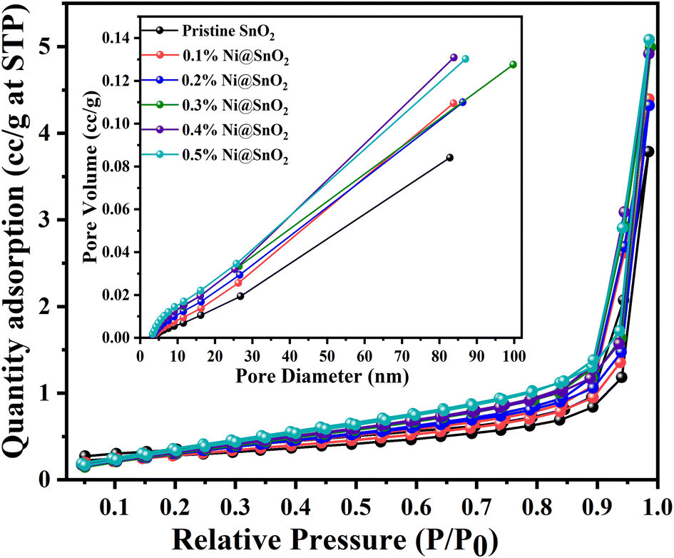 | ||
| Fig. 11 BET surface area graphs corresponding to the relative pressure for pristine SnO2 and Ni@SnO2 nanostructures (inset: pore size distribution curve). | ||
| Sample | BET surface area (m2 g−1) | Total pore volume (cm3 g−1) | BJH pore size (nm) | H2 generation (μmol g−1 h−1) |
|---|---|---|---|---|
| Pristine SnO2 | 9.9 | 0.0872 | 1.8820 | 8.52 |
| 0.1% Ni@SnO2 | 13.2 | 0.1139 | 1.6899 | 16.2 |
| 0.2% Ni@SnO2 | 15.1 | 0.1266 | 1.6834 | 25.67 |
| 0.3% Ni@SnO2 | 19.6 | 0.1316 | 1.6769 | 49.98 |
| 0.4% Ni@SnO2 | 18.2 | 0.1346 | 1.6811 | 39.78 |
| 0.5% Ni@SnO2 | 17.3 | 0.1351 | 1.6817 | 28.4 |
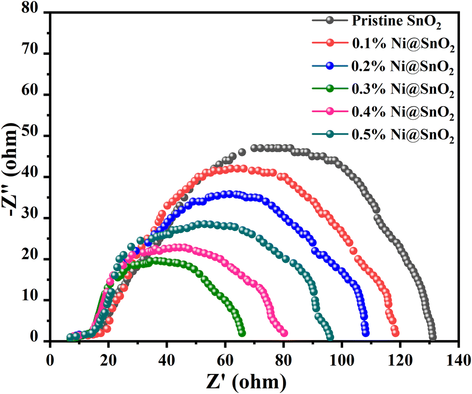
Photoelectrochemical study
Nyquist plot analysis furnishes a wide-ranging understanding of the interactions among charge transfer kinetics, recombination processes, and catalytic activity in defining the efficacy of hydrogen generation in photoelectrochemical systems. The typical plot is presented as a semicircle of a complex impedance plane, with superior potency indicated by a smaller semicircle at higher frequencies, which signifies fast charge transfer and a lower rate of recombination.75Pristine SnO2 exhibited the largest semicircle, with an electrochemical reaction resistance (Rct) of 130 Ω, while the lowest value of 65 Ω was observed for the 0.3%Ni@SnO2 composite (Fig. 12). The distinctly superior electrochemical performance observed in the Nyquist plot for 0.3%Ni@SnO2 compared with lower and higher Ni loading concentrations accentuates its potential as a propitious contender for photoelectrochemical hydrogen production applications (Fig. 12).
 | ||
| Fig. 12 Nyquist plot for SnO2 and 0.1 to 0.5% Ni@SnO2 nanostructures. | ||
Faster charge transfer kinetics at the electrode–electrolyte interface were demonstrated via the smaller semicircle in the Nyquist plot for 0.3% Ni@SnO2, which enables efficient conversion of photoexcited electrons to hydrogen ions, leading to higher hydrogen evolution rates. At lower Ni@SnO2 composite surface deposition concentrations, the insufficient loading levels lead to slower charge transfer kinetics, whereas at higher loading concentrations of Ni, increased surface deposition causes reorganization or electronic effects that hinder charge transfer; the optimum balance of both is achieved at 0.3% Ni loading.
Photoconductivity study
The I–V characteristics of pristine SnO2 and 0.3% Ni@SnO2 photodetectors with a voltage sweep of −10.0 V to 10.0 V are shown in Fig. 13a. The linear behaviour of all the I–V curves confirmed the generation of ohmic contact between the samples and the ITO electrodes. The observed photocurrents for the pristine SnO2 and 0.3% Ni@SnO2 photodetectors under the light illumination were 16.5 nA and 20.9 nA, respectively, compared to 10.91 nA for the same measurement in the dark for 0.3% Ni@SnO2 photodetectors. The nickel loading on the SnO2 surface effectively improved the charge transport, leading to an enhancement of the photocurrent. The photo-response of the pristine SnO2 and 0.3% Ni@SnO2 based photodetectors at 0.5 V bias voltage is shown in Fig. 13(b) for five cycles. Both the pristine SnO2 and 0.3% Ni@SnO2 sample based photodetectors showed a swift response to light with a constant and stable current over several cycles. The rise times observed for the pristine SnO2 and 0.3% Ni@SnO2 photodetectors under light illumination and dark conditions were found to be 800, 600 and 1200 ms, with corresponding fall times of 1210, 1000 and 1800 ms, respectively. The presence of nanoscale Ni loading on the SnO2 surfaces improves charge separation and introduces additional electrochemical reaction pathways or active sites, leading to an increase in the overall photocurrent response. | ||
| Fig. 13 (a) I–V characteristics and (b) photo-response of pristine SnO2 and 0.3% Ni@SnO2 photodetectors. | ||
Cyclic voltammetry (CV) profiles of SnO2 and 0.3%Ni@SnO2 were obtained (Fig. 14) to further probe their photoelectrochemical behaviour. Although the CV profiles did not exhibit the rectangular shape typically associated with ideal capacitive behaviour, the increase in current observed for the 0.3%Ni@SnO2 as compared to pristine SnO2 indicated an enhancement in photoelectrochemical activity. The higher current in the 0.3%Ni@SnO2 revealed the generation of a greater number of charge carriers and/or a more efficient charge transfer process, which could be directly correlated with an increase in charge storage capacity. Additionally, the larger area enclosed in the CV curves of 0.3%Ni@SnO2 signified higher capacitance, reflecting the material's ability to store and discharge more charge carriers.
 | ||
| Fig. 14 C–V measurement of pristine SnO2 and 0.3% Ni@SnO2 samples. | ||
Photocatalytic water splitting
Photocatalytic hydrogen generation trials were carried out by employing the Ni@SnO2 nanostructures under visible light irradiation in the water splitting reaction facilitated by a 20% aqueous methanol (v/v) solution, and the noteworthy conclusions are presented in Fig. 15. During the hydrogen evolution process, methanol plays dual roles, primarily as a sacrificial reagent to efficiently subdue the oxygen evolution rate, and secondly, participating in an irrevocable reaction with the photogenerated valence band holes from the semiconductor to reduce the rate of charge carrier recombination, which, in turn, assists in the amplification of photocatalytic activity.76 For the pristine SnO2 sample, a maximum hydrogen production of 24 μmol g−1 (in 3 h) was found, which was the smallest among all the samples (Fig. 15). The hydrogen production rate of Ni@SnO2 nanostructures at lower Ni loading concentrations were substantially small but exhibited a noteworthy increase with higher loading until the 0.3%Ni@SnO2 nanostructure sample. Above 0.3% Ni loading, a steady decline in the hydrogen production was noted. The hydrogen generation data for all samples are summarized in Table 1, and the highest hydrogen evolution rate was detected for the 0.3%Ni@SnO2 nanostructure with a value of 49.9 μmol h−1 g−1, which is ∼6 times higher than that for the pristine SnO2 sample. The achieved photocatalytic water splitting value for the 0.3%Ni@SnO2 nanostructure was found to be on par with reported values, as presented in Table 5. It may be noted that most of the reports presented in Table 5 deal with the doping of SnO2 with different materials. However, doping may not be an efficient process, due to the non-uniform distribution of dopants. Additionally, there are a few reports on the use of noble metals such as platinum on the SnO2 surface, which makes the process uneconomical. | ||
| Fig. 15 Photocatalytic hydrogen generation rates of the prepared pristine SnO2 and Ni@SnO2 nanostructures. | ||
| Sr. No. | SnO2-based Material | H2 generation yield μmol g−1 h−1 | Ref. |
|---|---|---|---|
| 1. | Boron-doped SnO2 | 63.6184 | 70 |
| 2. | Carbon-doped SnO2 | 38.43 | 82 |
| 3. | N-doped SnO2 | 42.5 | 83 |
| 4. | Pt/Ni(OH)2SnO2 | 0.9 | 26 |
| Pt/Ni(OH)2–Ni2O3–SnO2 | 10.8 | ||
| 5. | Ce–doped SnO2 nanoparticles | 25 | 84 |
| 6. | ZnO–SnO2 thin films | 14 (μmol h−1) | 85 |
| 7. | BiVO4 quantum dot decorated screw-like SnO2 nanostructures | 1.16 (μmol h−1 cm−2) | 86 |
| 8. | 0.3% Ni@SnO2 | 49.98 | Present work |
This increase in the photocatalytic performance can be attributed to the loading with Ni, an efficient noble metal (Pt)-free co-catalyst, effecting swift and effortless charge separation for surface-activated SnO2 semiconductor nanoparticle bands. It may be noted that Ni not only acts as a co-catalyst, but also interacts electronically, as inferred from Raman, UV-visible and PL spectroscopic data, probably creating directional charge transfer channels.77 The strong electronic interface between Ni-related surface states (playing a role similar to a dopant) and the SnO2 matrix material states through these channels affects the surface acceptor states, with ensuing negative charge at the semiconductor surface.51
The photocatalytic water splitting mechanism comprises sunlight absorption by semiconductor photocatalysts (SnO2) transferring electrons from the valence band (VB) to the conduction band (CB), leaving behind holes in the VB. These holes produce protons (H+) and radicals via the oxidization of methanol.78 Simultaneously, generation of molecular hydrogen by the reduction of protons through the electrons of the CB occurs by means of a sequence of reactions.79 However, this process occurs if rapid recombination of electrons and holes is retarded. In case of the pristine SnO2 sample, the observed low H2 production is attributable to the rapid recombination of such photogenerated charges. In the case of the Ni@SnO2 nanostructures, the significant enhancement in the hydrogen evolution with varying nickel loading concentrations in SnO2 can be ascribed to several aspects. Initially, the increase in nickel loading from 0.1% to 0.3% enhanced the density of active sites available on the surface of the SnO2 nanoparticles, which facilitated effective hydrogen evolution reaction (HER). Additionally, nickel acts as a co-catalyst for the HER due to its ability to adsorb hydrogen atoms and enable their combination to form hydrogen molecules, eliminating the need for the expensive Pt co-catalyst. At lower Ni loading concentrations, the presence of nickel enhances the catalytic activity of the SnO2 surface, promoting the HER. However, beyond 0.3% Ni loading, excessive nickel may result in the formation of inactive nickel clusters causing catalytic poisoning, leading to a decline in the catalytic activity and consequently, in the hydrogen evolution rate.
Noble metals such as Au, Ag, Pt, etc., have been reported to alter the electron distribution to improve SnO2-based photocatalytic H2 production.24 The conduction band level of the target matrix SnO2 (−0.42 eV), is higher than that of Ni (−0.23 eV) above the H2 evolution potentials, forming a Schottky barrier at the contact interface. Electrons drift from the high energy levels of SnO2 to Ni, which acts as an electron acceptor, confining the electrons, which in turn averts photogenerated charge carrier recombination.80,81 Consequently, the efficiency of photocatalytic H2 production by autocatalytically deposited Ni on the SnO2 photocatalyst surface was found to be greatly enhanced.24
It is worth noting that the obtained photocatalytic hydrogen production data was substantiated by the PL spectroscopy and BET results. In the PL results, the intensity of peaks corresponding to near-band-edge UV emission (364 nm) and defects (468 nm) were quenched due to generation of a non-radiative epicentre (Fig. 6). Additionally, the BET surface area increased until the Ni loading reached 0.3% and then decreased for the Ni@SnO2 nanostructures. Both these effects eventually affected the photocatalytic hydrogen production. CV data provided substantial evidence that Ni loading enhanced the charge capacitance of SnO2, indicating better electrochemical performance. However, further optimization is needed to achieve efficient solar hydrogen production.
Conclusion
A hitherto unreported Ni@SnO2 photocatalytic system active under visible light was prepared by the co-precipitation synthesis of SnO2 nanoparticles followed by autocatalytic Ni loading. The nickel loading was varied from 0.1 to 0.5 wt% on surface-activated SnO2 nanopowders. Ni was uniformly deposited as nanoparticles and surface coating onto the SnO2 nanopowder surface, as confirmed by FETEM equipped with EDS as well as XPS spectroscopy. The Ni2+ loading on the SnO2 nanopowder surface quenched the PL peak intensity and modified the defect band structure, leading to efficient photogenerated charge carrier separation. The significant improvement in photocatalytic H2 production for the Ni@SnO2 nanostructures compared to the pristine SnO2 nanoparticles could be ascribable to Schottky barrier formation between SnO2 to Ni and subsequent transfer of photogenerated electrons from the semiconductor to the metal. A maximum hydrogen generation of ∼50 μmol g−1 h−1 was recorded for the 0.3%Ni@SnO2 nanopowder, which was almost ∼6 greater more than the 8.52 μmol g−1 h−1 obtained for the pristine SnO2 nanopowder. The present work highlights the efficacy of the autocatalytic deposition technique in producing a hitherto unreported effective and economical Ni@SnO2-nanostructure-based heterogeneous photocatalyst. We optimistically believe that the autocatalytic deposition technique elaborated in the present study will represent an innovative pathway for surface decoration of exceedingly competent heterogeneous photocatalytic systems for semiconductor materials.Author contributions
The experiments have been planned & performed by P. N. B. under the supervision of B. K., who introduced the idea of electroless Ni plating. S. R., R. C. and S. G. have supported the characterization. The data were analysed by P. N. B., M. S. and S. A. All the authors have participated in writing the manuscript.Data availability
Data will be made available on request.Conflicts of interest
There are no conflicts to declare.Acknowledgements
One of the authors, Priyanka N. Birla, is thankful to Department of Science and Technology (DST) KIRAN Division, New Delhi, India, for DST Women Scientist fellowship (DST/WOS-A/CS-14/2021).References
- S. Bagheri and N. M. Julkapli, Int. J. Hydrogen Energy, 2020, 45, 31538–31554 CrossRef CAS.
- C. Wang and D. Astruc, Chem. Soc. Rev., 2021, 50, 3437–3484 RSC.
- F. Nadeem, H. Zhang, N. Tahir, Z. Zhang, R. R. Singhania, M. Shahzaib, H. Ramzan, M. Usman, M. Rahman and Q. Zhang, Bioresour. Technol., 2023, 382, 129221 CrossRef CAS PubMed.
- N. Bion, D. Duprez and F. Epron, ChemSusChem, 2012, 5, 76–84 CrossRef CAS PubMed.
- Y. Mao, Y. Gao, W. Dong, H. Wu, Z. Song, X. Zhao, J. Sun and W. Wang, Appl. Energy, 2020, 267, 114860 CrossRef CAS.
- X. Zhang, M. Shakeel, B. Li and L. Wang, Electrochim. Acta, 2020, 331, 135369 CrossRef CAS.
- N. Fajrina and M. Tahir, Int. J. Hydrogen Energy, 2019, 44, 540–577 CrossRef CAS.
- L. C. Goveas, S. Nayak, R. Vinayagam, R. Selvaraj and A. Pugazhendhi, Fuel, 2023, 348, 128460 CrossRef CAS.
- S. Sahani, K. M. Tripathi, T. I. Lee, D. P. Dubal, C.-P. Wong, Y. C. Sharma and T. Y. Kim, Energy Convers. Manage., 2022, 252, 115133 CrossRef CAS.
- B. Guan, J. Yu, S. Guo, S. Yu and S. Han, Nanoscale Adv., 2020, 2, 1352–1357 RSC.
- J. Kegel, I. M. Povey and M. E. Pemble, Nano Energy, 2018, 54, 409–428 CrossRef CAS.
- M. B. Costa, M. A. de Araújo, M. V. D. L. Tinoco, J. F. D. Brito and L. H. Mascaro, J. Energy Chem., 2022, 73, 88–113 CrossRef CAS.
- C. M. Suarez, S. Hernández and N. Russo, Appl. Catal., A, 2015, 504, 158–170 CrossRef.
- S. H. Chen, Y. S. Jiang and H. Y. Lin, ACS Omega, 2020, 5, 8927–8933 CrossRef CAS PubMed.
- X. Zheng, L. Feng, Y. Dou, H. Guo, Y. Liang, G. Li, J. He, P. Liu and J. He, ACS Nano, 2021, 15, 13209–13219 CrossRef CAS.
- S. Wu, J. Sun, Q. Li, Z. D. Hood, S. Yang, T. Su, R. Peng, Z. Wu, W. Sun, P. R. C. Kent, B. Jiang and M. F. Chisholm, ACS Appl. Mater. Interfaces, 2020, 12, 20067–20074 CrossRef CAS.
- J. Yadav, P. Raturi, S. Yadav and J. P. Singh, Renewable Energy, 2021, 179, 2256–2266 CrossRef CAS.
- V. Hasija, P. Raizada, A. Hosseini-Bandegharaei, V. K. Thakur, Q. Van Le, V. H. Nguyen and P. Singh, ChemCatChem, 2021, 13, 2965–2987 CrossRef CAS.
- Y. Xu, D. Li, Q. Zeng, H. Sun and P. Li, RSC Adv., 2023, 13, 27676–27685 RSC.
- A. Chauhan, Sonu, P. Raizada, P. Singh, T. Ahamad, V.-H. Nguyen, Q. V. Le, A. A. P. Khan, N. Kumar, A. Sudhaik and C. M. Hussain, J. Ind. Eng. Chem., 2024, 130, 25–53 CrossRef CAS.
- J. A. Nasir, Z. U. Rehman, S. N. A. Shah, A. Khan, I. S. Butler and C. R. A. Catlow, J. Mater. Chem. A, 2020, 8, 20752–20780 RSC.
- S. Singh and S. K. Kansal, Appl. Mater. Today, 2022, 26, 101345 CrossRef.
- H. Luo, Z. Zeng, G. Zeng, C. Zhang, R. Xiao, D. Huang, C. Lai, M. Cheng, W. Wang, W. Xiong, Y. Yang, L. Qin, C. Zhou, H. Wang, Y. Zhou and S. Tian, Chem. Eng. J., 2020, 383, 123196 CrossRef CAS.
- C. Sun, J. Yang, M. Xu, Y. Cui, W. Ren, J. Zhang, H. Zhao and B. Liang, Chem. Eng. J., 2022, 427, 131564 CrossRef CAS.
- S. Das and V. Jayaraman, Prog. Mater. Sci., 2014, 66, 112–255 CrossRef CAS.
- Q. Du and G. Lu, Appl. Surf. Sci., 2014, 305, 235–241 CrossRef CAS.
- Y. Y. Li, B. X. Zhou, H. W. Zhang, S. F. Ma, W. Q. Huang, W. Peng, W. Hu and G. F. Huang, Nanoscale, 2019, 11, 6876–6885 RSC.
- Y.-Y. Li, B.-X. Zhou, H.-W. Zhang, T. Huang, Y.-M. Wang, W.-Q. Huang, W. Hu, A. Pan, X. Fan and G.-F. Huang, Chem. Eng. J., 2022, 430, 132880 CrossRef CAS.
- A. Mamakhel, M. Søndergaard, K. Borup and B. B. Iversen, J. Supercrit. Fluids, 2020, 166, 105029 CrossRef CAS.
- S. Naz, I. Javid, S. Konwar, K. Surana, P. K. Singh, M. Sahni and B. Bhattacharya, SN Appl. Sci., 2020, 2, 2–9 CrossRef.
- G. H. Patel, S. H. Chaki, R. M. Kannaujiya, Z. R. Parekh, A. B. Hirpara, A. J. Khimani and M. P. Deshpande.
- S. Das, K. G. Girija, A. K. Debnath and R. K. Vatsa, J. Alloys Compd., 2021, 854, 157276 CrossRef CAS.
- N. Nabihah-Fauzi, N. Asikin-Mijan, M. L. Ibrahim, H. Hashim, S. Yusup, Y. H. Taufiq-Yap and M. S. Mastuli, RSC Adv., 2020, 10, 29187–29201 RSC.
- J. Liu, K. Kempa and J. Gao.
- R. B. Rajput and R. B. Kale, Environ. Adv., 2021, 5, 100081 CrossRef CAS.
- I. Ullah, A. Munir, S. Muhammad, S. Ali, N. Khalid, M. Sirajuddin, S. Z. Hussain, S. Ahmed, Y. Khan, I. Hussain, A. Haider, A. Munir, S. Muhammad, S. Ali, N. Khalid, M. Zubair, M. Sirajuddin, S. Z. Hussain, S. Ahmed, Y. Khan, I. Hussain and A. Haider, J. Alloys Compd., 2020, 827, 154247 CrossRef CAS.
- Y. C. Chang, C. Y. Yan and R. J. Wu, J. Chin. Chem. Soc., 2014, 61, 345–349 CrossRef CAS.
- I. Marić, G. Dražić, E. Radin, R. Peter, M. Škrabić, T. Jurkin, A. Pustak, N. Baran, L. Mikac, M. Ivanda, M. Petravić, G. Štefanić and M. Gotić, Appl. Surf. Sci., 2023, 607, 155073 CrossRef.
- Y. Sun, Q. Zhu, B. Bai, Y. Li and C. He, Chem. Eng. J., 2020, 390, 124518 CrossRef CAS.
- H. Wang, K. Zhang, J. Qiu, J. Wu, J. Shao, Y. Deng, Y. Wu and L. Yan, Energy Fuels, 2021, 35, 12516–12526 CrossRef CAS.
- Y. Ye, Y. Wang, Z. Li, Y. Ye, Y. Liu, X. Zou and S. Lin, New J. Chem., 2019, 43, 17023–17032 RSC.
- G. O. Testoni, R. A. C. Amoresi, G. M. M. M. Lustosa, J. P. C. Costa, M. V. Nogueira, M. Ruiz, M. A. Zaghete and L. A. Perazolli, Solid State Sci., 2018, 76, 65–73 CrossRef CAS.
- S. Jana, S. Konar, B. C. Mitra, A. Mondal and S. Mukhopadhyay, Mater. Res. Bull., 2021, 141, 111351 CrossRef CAS.
- V. S. Suvith, V. S. Devu and D. Philip, Ceram. Int., 2020, 46, 786–794 CrossRef CAS.
- W. Zhang, Y. Yu, R. Huang and X. Shi, ACS Appl. Mater. Interfaces, 2021, 13, 40571–40581 CrossRef CAS PubMed.
- T. Qiu and P. K. Chu, Mater. Sci. Eng., R, 2008, 61, 59–77 CrossRef.
- Ş. Neaţu, F. Neaţu, V. C. Diculescu, M. M. Trandafir, N. Petrea, S. Somacescu, F. Krumeich, J. T. C. Wennmacher, A. J. Knorpp, J. A. Van Bokhoven and M. Florea, ACS Appl. Mater. Interfaces, 2020, 12, 18407–18420 CrossRef.
- P. N. Birla, S. Arbuj, M. D. Shinde, S. Joseph, S. Rane, S. Kulkarni and B. Kale, RSC Adv., 2023, 13, 20068–20080 RSC.
- T. Boettcher, S. Schaefer, M. Antoni, T. Stohr, U. Kunz, M. Dürrschnabel, L. Molina-Luna, W. Ensinger and F. Muench, Langmuir, 2019, 35, 4246–4253 CrossRef CAS PubMed.
- F. Muench, ChemElectroChem, 2021, 8, 2993–3012 CrossRef CAS.
- K.-I. Choi, M. Hübner, A. Haensch, H.-J. Kim, U. Weimar, N. Barsan and J.-H. Lee, Sens. Actuators, B, 2013, 183, 401–410 CrossRef CAS.
- M. Kandasamy, A. Seetharaman, D. Sivasubramanian, A. Nithya, K. Jothivenkatachalam, N. Maheswari, M. Gopalan, S. Dillibabu and A. Eftekhari, ACS Appl. Nano Mater., 2018, 1, 5823–5836 CrossRef CAS.
- K. K. Supin, A. George, Y. R. Kumar, K. K. Thejas, G. Mandal, A. Chanda and M. Vasundhara, RSC Adv., 2022, 12, 26712–26726 RSC.
- A. Mohammad, M. E. Khan, M. R. Karim, M. H. Cho and T. Yoon, Ceram. Int., 2021, 47, 23578–23589 CrossRef CAS.
- L. M. Jose, N. S. George, S. A. Kadam, S. Athira, A. Kripa, A. Aravind, Y.-R. Ma and Y.-R. Chen, Opt. Mater., 2023, 135, 113348 CrossRef CAS.
- X. Wei, C. Wan, Y. Zhang, Q. Zhong and H. Qu, Int. J. Hydrogen Energy, 2023, 48, 36403–36411 CrossRef CAS.
- L. Fan, P. F. Liu, X. Yan, L. Gu, Z. Z. Yang, H. G. Yang, S. Qiu and X. Yao, Nat. Commun., 2016, 7, 1–7 Search PubMed.
- F. H. Aragón, J. A. H. Coaquira, P. Hidalgo, S. W. Da Silva, S. L. M. Brito, D. Gouvêa and P. C. Morais, J. Raman Spectrosc., 2011, 42, 1081–1086 CrossRef.
- A. Diéguez, A. Romano-Rodríguez, A. Vilà and J. R. Morante, J. Appl. Phys., 2001, 90, 1550–1557 CrossRef.
- I. M. Costa, Y. N. Colmenares, P. S. Pizani, E. R. Leite and A. J. Chiquito, Chem. Phys. Lett., 2018, 695, 125–130 CrossRef CAS.
- L. Ying-Kai, D. Yi and W. Guang-Hou, Chin. Phys. Lett., 2004, 21, 156 CrossRef.
- Y. Fu, J. Li and H. Xu, Mater. Sci. Semicond. Process., 2020, 114, 105073 CrossRef CAS.
- S. Mehraj, M. S. Ansari and Alimuddin, Thin Solid Films, 2015, 589, 57–65 CrossRef CAS.
- N. Bhardwaj, B. Satpati and S. Mohapatra, Appl. Surf. Sci., 2020, 504, 144381 CrossRef CAS.
- P. Chetri and A. Choudhury, Phys. E, 2013, 47, 257–263 CrossRef CAS.
- A. G. Habte, F. G. Hone and F. B. Dejene, Physica B: Condens. Matter, 2020, 580, 411832 CrossRef CAS.
- J. Park, S. S. Lam, Y.-K. Park, B.-J. Kim, K.-H. An and S.-C. Jung, Environ. Res., 2023, 216, 114657 CrossRef CAS.
- S. Sen, S. Maity and S. Kundu, J. Alloys Compd., 2023, 966, 171553 CrossRef CAS.
- P. Renganathan, S. Marimuthu, R. Kanniah, V. Karthikeyan and G. A. Sundaram, Results Chem., 2022, 4, 100557 CrossRef CAS.
- S. Kumar, Bhawna, S. K. Yadav, A. Gupta, R. Kumar, J. Ahmed, M. Chaudhary, Suhas and V. Kumar, Environ. Sci. Pollut. Res., 2022, 29, 47448–47461 CrossRef CAS PubMed.
- D. Chen, S. Huang, R. Huang, Q. Zhang, T. T. Le, E. Cheng, R. Yue, Z. Hu and Z. Chen, J. Hazard. Mater., 2019, 368, 204–213 CrossRef CAS PubMed.
- B. Lei, H. Zhang, W. Liu, Q. Zhao, Y. Wei, Y. Lu, X. Yang, W. Zhang, T. Xiao, J. Kong and W. Cai, Sens. Actuators, B, 2024, 401, 134907 CrossRef CAS.
- J. Shi, N. Lin, D. Liu, Y. Wang and H. Lin, J. Electroanal. Chem., 2020, 857, 113634 CrossRef CAS.
- L. Sang, G. Xu, Z. Chen, X. Wang, H. Cui, G. Zhang and Y. Dou, Mater. Sci. Semicond. Process., 2020, 105, 104710 CrossRef CAS.
- N. O. Laschuk, E. B. Easton and O. V. Zenkina, RSC Adv., 2021, 11, 27925–27936 RSC.
- K. Sathiyan, R. Bar-Ziv, V. Marks, D. Meyerstein and T. Zidki, Chem. – Eur. J., 2021, 27, 15936–15943 CrossRef CAS PubMed.
- B. Li, Z. Tian, L. Li, Y. H. Wang, Y. Si, H. Wan, J. Shi, G. F. Huang, W. Hu, A. Pan and W. Q. Huang, ACS Nano, 2023, 17, 3465–3482 CrossRef CAS PubMed.
- J. Zhao, R. Shi, Z. Li, C. Zhou and T. Zhang, Nano Sel., 2020, 1, 12–29 CrossRef.
- Y. Zhang, Y. Dai, H. Li, L. Yin and M. R. Hoffmann, Commun. Mater., 2020, 1, 1–9 CrossRef.
- L. Yang, J. Huang, L. Shi, L. Cao, W. Zhou, K. Chang, X. Meng, G. Liu, Y. Jie and J. Ye, Nano Energy, 2017, 36, 331–340 CrossRef CAS.
- Y. Y. Li, J. G. Wang, H. H. Sun, W. Hua and X. R. Liu, Int. J. Hydrogen Energy, 2018, 43, 14121–14129 CrossRef CAS.
- K. Mallikarjuna, G. A. K. M. Rafiqul Bari, S. V. P. Vattikuti and H. Kim, Int. J. Hydrogen Energy, 2020, 45, 32789–32796 CrossRef CAS.
- Bhawna, A. Gupta, P. Kumar, A. Tyagi, R. Kumar, A. Kumar, P. Singh, R. P. Singh and V. Kumar, ChemistrySelect, 2020, 5, 7775–7782 CrossRef CAS.
- V. Kumar, Bhawna, S. K. Yadav, A. Gupta, B. Dwivedi, A. Kumar, P. Singh and K. Deori, ChemistrySelect, 2019, 4, 3722–3729 CrossRef CAS.
- A. Saldaña-Ramírez, M. R. A. Cruz, I. Juárez-Ramírez and L. M. Torres-Martínez, Opt. Mater., 2020, 110, 110501 CrossRef.
- M. Xie, Z. Zhang, W. Han, X. Cheng, X. Li and E. Xie, J. Mater. Chem. A, 2017, 5, 10338–10346 RSC.
Footnote |
| † Electronic supplementary information (ESI) available. See DOI: https://doi.org/10.1039/d4nr01194e |
| This journal is © The Royal Society of Chemistry 2024 |