
Shape-controlled, water-assisted synthesis of 2D luminescent CsPb2Br5 perovskite microcrystals for highly responsive UV detectors†
Dipayan
Ray
a,
Ankush
Saini
b,
Ankit
Kumar
a,
Sumit
Kumar
a,
Monojit
Bag
 *b and
Prasenjit
Kar
*a
*b and
Prasenjit
Kar
*a
aDepartment of Chemistry, Indian Institute of Technology Roorkee, Roorkee, Uttarakhand, India. E-mail: kar.prasen@gmail.com; prasenjit.kar@cy.iitr.ac.in
bDepartment of Physics, Indian Institute of Technology Roorkee, Roorkee, Uttarakhand, India. E-mail: monojit.bag@ph.iitr.ac.in
First published on 26th October 2024
Abstract
Cesium–lead–halide (Cs–Pb–Br) perovskites have been a point of interest for researchers since their discovery for their extraordinary optical and electronic properties. Unlike other members of the Cs–Pb–Br family, CsPb2Br5 is less explored. Herein, we synthesized 2D CsPb2Br5 in an aqueous medium under ambient conditions. The fabrication was confirmed via several characterization techniques. Optical characterization was performed using UV, PL, and TCSPC analysis. Morphological study was conducted using FE-SEM and TEM analysis, which revealed a new square-pyramidal-like morphology. The structural stability of the material under ambient conditions was studied for an extended period to show its reliability in a practical environment. Moreover, the synthesized microcrystals were utilized to fabricate a highly responsive UV detector with significantly low rise and fall times of 1.2 and 2.6 ms, respectively, and a detectivity of 2.36 × 10⁸ Jones.
Introduction
Lead halide perovskites are among the promising candidates for the future of low-cost and efficient optoelectronic devices such as light-emitting diodes (LED), solar cells, photodetectors, and lasers.1 Similar to organic–inorganic hybrid perovskites and their promising optoelectronic excellence, metal halide perovskites have been widely researched in recent years.2–4 However, all-inorganic perovskites show better thermal, moisture, and photo-stability.5 Their organic counterparts are responsible for the fact that the quality of organic–inorganic perovskites is deleterious under ambient conditions and they struggle to maintain structural integrity at elevated temperatures. This appears to be a significant constraint of these materials in their implementation in LEDs and other optoelectronic applications.6–9 For the same reason, when the organic counterpart is replaced with an inorganic monovalent ion (like Cs+) in all-inorganic perovskites, it is known to provide better thermal and moisture stability. Cs–Pb–Br perovskite comes under the category of all-inorganic perovskites.10 There are three members in this family: 3D CsPbBr3, 2D CsPb2Br5, and 0D Cs4PbBr6. Properties such as a size-tunable band gap, exceptional adsorption, and extensive charge transport properties such as higher carrier lifetime with better charge carrier mobility, excellent photoluminescence quantum yield (PLQY), finer color purity, elongated carrier diffusion length, and narrow emission make this family the best fit for advanced optoelectronic applications.11–25 This unleashes the possibility for Cs–Pb–Br perovskite materials to be used in applications ranging from photovoltaics, lasers, photodetectors, X-ray detection, and encryption–decryption to acting as a photocatalyst in the reduction of CO2, hydrogen evolution, contaminant degradation, and organic synthesis.12,24,26Unlike CsPbBr3, CsPb2Br5, a new 2D member of the perovskite family, is comparatively less explored and exhibits unique optical and electronic properties, which has drawn the attention of researchers. The crystal structure of CsPb2Br5 is well explored in the literature. CsPb2Br5 exhibits a 2D tetragonal crystal system (I4/mcm space group), where the Pb layer is separated by the Cs layer. These Cs and Pb layers are alternatively stacked upon each other along the c-axis as shown in Fig. 1b. The Pb layer comprises Pb2Br5. In contrast to conventional 2D semiconductors, in this case, Cs does not rely on weak van der Waals bonding but demonstrates strong covalent bonding with Br. The growth of the Pb layer perpendicular to the c-axis is much higher than the growth of Cs layer parallel to the c-axis, which is an example of anisotropic growth. Each Cs forms a bicapped square prism with ten Br atoms. On the other hand, Pb forms a bicapped trigonal prism with 8 Br atoms. On average each Cs and Pb atom is bound to 8 and 6 Br atoms, respectively, which is totally different from the CsPbBr3 coordination structure.27 Generally, CsPb2Br5 is formed as a byproduct of the synthesis of the CsPbBr3 and Cs4PbBr6, as their formation energy lies in almost the same range. For this reason, the physical properties like stability and photoluminescence are controversial and the formation of pure CsPb2Br5 is a challenge.24
 | ||
| Fig. 1 (a) Schematic representation of the synthesis strategy. (b) Crystallographic structure of CsPb2Br5: (i and ii) side and top views of the CsPb2Br5 unit cell in a polyhedral model, (iii and iv) single and layered structure of the Pb subunit, and (v and vi) single and layered structure of the Cs subunit (green = Cs+, black = Pb2+, and brown = Br−). (c) Different stages of the microcrystal due to the arrest of crystal growth: direction of the crystal growth of Cs and Pb layers and decreasing growth of the Pb2Br5− layer resulting in the formation of the square pyramidal shape of CsPb2Br5 microcrystals. | ||
In the last few years, several efforts have been made to synthesize CsPb2Br5. CsPb2Br5 nanoplatelets were synthesized by Wang et al. They demonstrated the quick anion exchange and tuneable photoluminescence (PL) of the material throughout the visible spectrum. For the formation of the nanoplatelets, they employed toluene as an antisolvent and DMF as a solvent.28 Zhu et al. employed a ligand-assisted reprecipitation (LARP) technique, employing methanol and hexylamine as solvents and conducting the process at a temperature between 70 and 60 °C. They reported significantly high PLQY and fabricated a light emitting diode (LED).11 Zhang et al. synthesized pure CsPb2Br5 single crystal and used it to fabricate a highly sensitive photodetector by following the thermodynamic equilibrium growth condition. To achieve CsPb2Br5 crystallization, CsBr and PbBr2 were dissolved in deionised water and HBr separately and then mixed under heating and cooling.27 In contrast, Maity and coworkers presented a solvent-free mechanochemical synthesis method.29 To enhance the optoelectronic and thermal stability, CsPb2Br5 nanocrystals (NCs) were encapsulated in mesoporous silica by Shao et al. They designed a white LED to demonstrate the applicability of the material.30 Dual-phase CsPbBr3–CsPb2Br5 single crystal was prepared by Lin et al. Eventually, they fabricated a highly responsive photodetector with high photocurrent.31
Researchers have fabricated CsPb2Br5via the LARP method in HBr medium as well as in water–ethanol hybrid medium and via hot injection using water or octadecane (ODE) as the solvent.27,32–34 Various morphologies have been documented utilizing these techniques in recent years, ranging from square sheets to nanosheets to deformed square sheet-like structures.31,32,35,36 However, the synthesis of CsPb2Br5 in pure form solely in water at room temperature remains uncharted owing to the possibility of degradation of the formed product.
Here, we present a facile and inexpensive synthetic approach for synthesizing pure CsPb2Br5 in an aqueous medium (Fig. 1a). The reaction was carried out at ambient temperature and atmospheric pressure. The solubility of PbBr2 in water is problematic. To overcome this, we employed concentrated HBr (aq. 48%) and a higher amount of CsBr, as described in prior reports.33 In the presence of an excess of Br, PbBrn2−n is formed (where n ≥ 3 and is an integer), which is known to be water-soluble and plays a crucial role in the crystal growth (Fig. 1c), discussed in the Results and discussion section.27,37 Furthermore, we present a morphology that resembles a square pyramid. We examined the optoelectronic characteristics of the obtained CsPb2Br5 using various characterisation techniques like UV-Visible (UV-Vis) spectroscopy, PLQY analysis, time correlated single photon counting (TCSPC), and PL spectroscopy. We performed field emission scanning electron microscopy (FE-SEM) and transmission electron microscopy (TEM) to determine the morphology. X-ray photoelectron spectroscopy (XPS) and energy dispersive X-ray (EDX) analysis were implemented to confirm the presence of all constituent elements. X-ray diffraction (XRD) analysis was performed to reveal its crystal structure and phases. Thermal stability has been investigated using thermogravimetric analysis (TGA). Stability studies using XRD analysis have also been conducted for several days and indicate promising structural stability under ambient conditions. Using the synthesized microcrystals, a highly sensitive UV detector with a detectivity of 2.36 × 10⁸ Jones is prepared. The detector is highly responsive and has a rise time of 1.2 ms and a fall time of 2.6 ms.
Results and discussion
Following the synthesis of the material, we used a number of optical, morphological, and elemental characterization methods to verify that CsPb2Br5 has been successfully formed (Fig. 2).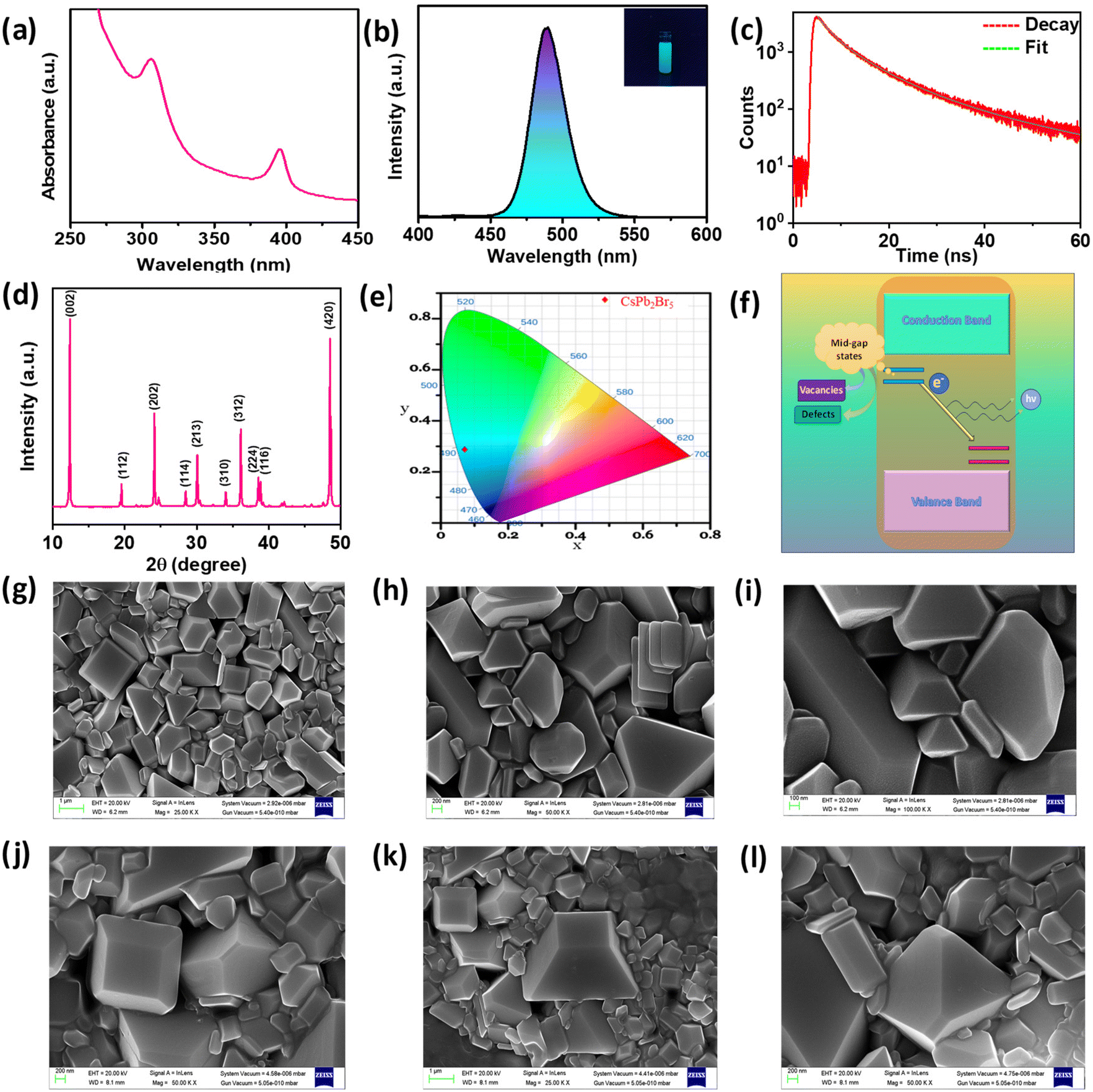 | ||
| Fig. 2 (a) Absorption (UV-vis), (b) emission (inset photograph) (PL), and (c) TCSPC spectra. (d) XRD pattern. (e) CIE co-ordinates. (f) Photoluminescence mechanism. (g–i) SEM images at different magnifications. (j–l) Different stages of microcrystals. | ||
A thorough understanding of the optical behavior and device application of the synthesized CsPb2Br5 was derived from the study of its optoelectronic characteristics. We investigated the absorption and emission characteristics of the material using UV-Vis and PL analysis (Fig. 2a–c). As shown in Fig. 2a, the UV-Vis spectrum has two distinct peaks at 305 nm and 395 nm, which agrees well with the previous reports. With the help of the Tauc plot, we calculated the band gap of the microcrystals. We calculated the values of (αhν) and plotted the (αhν)1/2vs. energy (eV) graph. The peak at 395 nm corresponds to the bandgap of 3.76 eV. According to Zhang et al. this wide bandgap near 3.8 eV corresponds to CsPb2Br5.27 Additionally, the emission property was examined (Fig. 2b). A sharp peak was observed around 489 nm (λex = 340 nm) which fits well with the previous report.38 The color purity of the light (Fig. 2e) was investigated by CIE (Commission Internationale de l’Éclairage), which implies that the material is capable of being used in optoelectronic devices. Although CsPb2Br5 is said to be an indirect band gap material in the literature, the green PL that results from it is debatable and occasionally ascribed to the trace amounts of CsPbBr3 that occur on the surface of CsPb2Br5.39
However, in our case, the absence of CsPbBr3 is confirmed by the results of XRD, SEM, and EDX, as discussed later in the paper. According to Jiang et al., this green emission arises from the mid-gap states. Mid-gap states (Fig. 2f) are the results of vacancies and antisite defects.5 This is also confirmed by the fact that Zhang et al. guessed that the absorbance of 320–370 nm is probably due to defects. In Fig. 2c, from the TCSPC analysis, we can observe the time-resolved photoluminescence decay. The fluorescence lifetime decay curve is fitted in tri-exponential. The curve has three components, fast, moderate, and slow, as shown in Table S2.† The lifetime of these components is 2.36, 6.66, and 19.7 ns, respectively. The calculated average lifetime is 10.4 ns.
To confirm the successful formation of CsPb2Br5, XRD analysis was performed (Fig. 2d). Sharp and prominent peaks revealed by the XRD analysis confirm the high crystallinity and quality of the synthesized material. All the peaks are identified and compared with the previously reported XRD of pure CsPb2Br5.27,40 CsPb2Br5 has a tetragonal I4/mcm phase with the peaks at 12.46°, 19.77°, 24.35°, 28.28°, 30.12°, 34.10°, 36.3°, 38.59°, 38.94°, and 48.50° corresponding to the planes (002), (112), (202), (114), (213), (310), (312), (224), (116), and (420), respectively (Fig. 2d).27
However, several reports from the previous literature highly suggest the coexistence of the CsPbBr3 phase with CsPb2Br5 as a by-product. So, the production of the pure CsPb2Br5 phase is a tedious job. To confirm the purity of our material, we have compared the obtained XRD pattern with that of the pure CsPb2Br5 phase and there was no extra peak of impurity or the characteristic peak of CsPbBr3 around 15° was absent.
The morphological characteristics were investigated by FE-SEM analysis. FE-SEM images were collected at various magnifications to better comprehend the morphology (Fig. 2g–i). The surface structure is revealed where we found that our synthesized CsPb2Br5 has square pyramid-like blocks, unlike previous reports which show mostly a square sheet-like geometry.31,36,40 The different stages of the microcrystal can be seen in Fig. 2j–l. The square-pyramidal-like morphology has still not been reported to the best of our knowledge. EDX analysis is further performed to establish the elemental composition of the material, which reveals a ratio of around 1![[thin space (1/6-em)]](https://www.rsc.org/images/entities/char_2009.gif) :2:5 for Cs:Pb:Br (Table S1†). To better understand the morphology and structure of the synthesised material we have acquired HR-TEM images which clearly show the 2D projection of the square pyramidal geometry. In Fig. 3a, b, and c, we can see the TEM image of the microcrystals, and fringes obtained from HR-TEM analysis, followed by the SAED pattern, respectively. In Fig. 3d–j, TEM images at different magnifications (100 nm, 200 nm, and 500 nm) are acquired to provide insight into the morphology of the material. The elemental mapping of the material is shown in Fig. 3j and k. From Fig. 3b we have observed a lattice spacing of 0.59 nm, corresponding to the (110) plane of CsPb2Br5 which agrees well with the previous reports.34,41 From the SAED pattern, we found the presence of (220) and (020) planes corresponding to the d-spacing value of 0.291 nm and 0.426 nm, which agrees well with the d-spacing calculated from the XRD pattern.28,40,42
:2:5 for Cs:Pb:Br (Table S1†). To better understand the morphology and structure of the synthesised material we have acquired HR-TEM images which clearly show the 2D projection of the square pyramidal geometry. In Fig. 3a, b, and c, we can see the TEM image of the microcrystals, and fringes obtained from HR-TEM analysis, followed by the SAED pattern, respectively. In Fig. 3d–j, TEM images at different magnifications (100 nm, 200 nm, and 500 nm) are acquired to provide insight into the morphology of the material. The elemental mapping of the material is shown in Fig. 3j and k. From Fig. 3b we have observed a lattice spacing of 0.59 nm, corresponding to the (110) plane of CsPb2Br5 which agrees well with the previous reports.34,41 From the SAED pattern, we found the presence of (220) and (020) planes corresponding to the d-spacing value of 0.291 nm and 0.426 nm, which agrees well with the d-spacing calculated from the XRD pattern.28,40,42
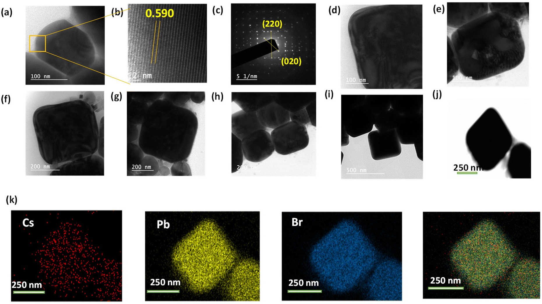 | ||
| Fig. 3 TEM images of CsPb2Br5 (a) at 100 nm, (b) fringes at 2 nm, (c) SAED pattern, (d and e) images at 100 nm, (f–h) images at 200 nm, (i) image at 500 nm, and (j and k) elemental mapping of the microcrystal. | ||
As mentioned, we have used PbBr2 and CsBr in 2:5.5 initially, which is contradictory if we consider the final product where the Pb:Cs ratio is 2:1. But, at the first stage of the reaction, when we mix Pb and Cs salts together, in the span of 1 hour the salts get dissolved in the reaction mixture, forming a white solution. After 1 hour, when we add acetone to the reaction mixture the Pb2+ and Cs+ get precipitated, making the solution transparent. The white solution does not exhibit any luminescence. This suggests that the formation of CsPb2Br5 has not started at this stage. Now as per Yin et al. the solubility of Cs+ in water is much higher than that of Pb2+ in water.40 So, during precipitation, the precipitation rate of Pb2+ is higher than that of Cs+. At the initial stage, due to the higher precipitation rate of Pb2+, the concentration of Pb2+ is higher than that of Cs+, which facilitates the formation of the Pb2Br5− layer rapidly, which grows in the direction perpendicular to the c-axis, i.e., in the ab-plane. As the time passes, the concentration of Cs+ surpasses the concentration of Pb2+. The Cs+ layer grows parallel to the c-axis and has a much lower rate of growth than the Pb2+ layer. On the other hand, the Pb2+ is the limiting reagent, i.e., the amount of Pb2+ in the total reaction mixture is lower than that of Cs+. After a certain point, the Pb2+ layer growth starts to decrease due to the scarcity of Pb concentration. However, the supply of Cs+ remains constant due to its higher amount in the reaction mixture. Hence, the growth of Cs+ along the c-axis continues until the Pb2+ is used up. Due to the constant growth of the c-axis and gradually decreasing growth of the ab-axis, the crystal forms a square pyramidal-like morphology, in which some of the crystal growth stops at stage i, and some crystal growth is complete and forms stage iv (Fig. 1c). Owing to this, a mixture of all four different stages of the microcrystals was observed. If the Cs and Pb were present in the same molar amount, it would have formed a flake-like morphology.27
To validate the existence of all constituent elements, XPS analysis was performed. The survey scan is given in Fig. S4.† Two peaks for Cs appear at 738.20 and 723.98 eV (Fig. 4a). Those two peaks are attributed to 3d3/2 and 3d5/2, respectively. Peaks for Pb 4f appear at 143.07 and 138.11 eV, which correspond to 4f5/2 and 4f7/2, respectively (Fig. 4b). In the case of Br, 3d3/2 and 3d5/2 peaks can be seen at 68.96 and 67.87 eV (Fig. 4c). This confirms that all the constituent atoms are in their desired valence state.24
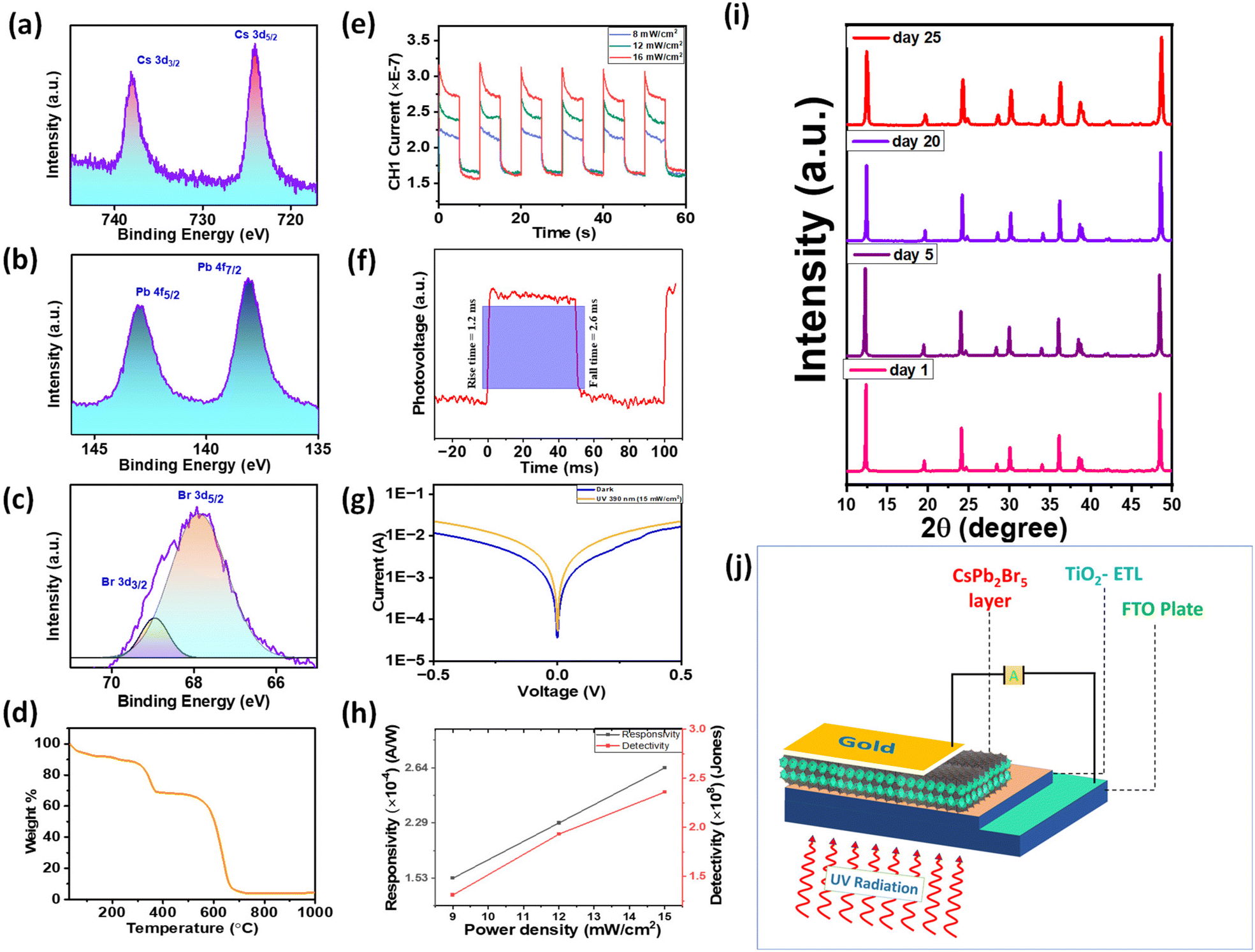 | ||
| Fig. 4 XPS spectra of CsPb2Br5: (a) narrow scan of Cs, (b) narrow scan of Pb, and (c) narrow scan of Br. (d) TGA spectra, (e) photoresponse study (current–time graph) at different light intensities, (f) photoresponse for the rise and fall time, (g) I–V characteristics of the photodetector under light and dark conditions, (h) responsivity and detectivity of the photodetector, (i) time-dependent XRD pattern and (j) schematic of the fabricated UV-photodetector. | ||
To ensure the structural stability, time-dependent XRD was performed. The XRD of the 25th day does not have any extra peak, which confirms the stability of the material in the mentioned period (Fig. 4i). The thermal stability of the as-synthesized CsPb2Br5 was examined by TGA (Fig. 4d). From the TGA curve we can see that there are three main degradation peaks. The first one, close to 100 °C, is due to the loss of moisture, which is less significant than the other two. The second decrement around 300 °C is due to the elimination of surface-bound ligands and at 600 °C the last decrement can be attributed to the structural disintegration of the perovskite structure.
The performance of the photodetector was measured using a UV (380 nm) SMD LED light source driven by a Keysight function generator. To quantify the performance of the photodetector, measurements were also taken with different incident power densities. Fig. 4e shows the response of the prepared photodetector device under the illumination of 380 nm wavelength light under different light intensities. Further to characterize and compare the performance of a photodetector, various parameters such as rise/fall time, responsivity, and specific detectivity need to be taken into consideration. Detection speed is an important parameter of a photodetector which is measured by the time photocurrent takes to reach 10% and 90% of its saturation level upon switching the light on and off. To measure the rise and fall time of the device we carried out the transient photovoltage measurement of the device under 16 mW cm−2 UV light intensity using an oscilloscope. The rise and fall times of the device as shown in Fig. 4f are 1.2 ms and 2.6 ms, respectively, which are comparable to and even faster than those of many previously reported all inorganic CsPb2Br5 perovskite nanocrystal-based photodetectors as shown in Table 1.
Responsivity, indicating the efficiency of a photodetector in responding to incoming light, is defined as the ratio of the generated photocurrent to the incident light power on the device's active area. It is expressed as R = Jph/Pinc = (Ilight − Idark)/(Pinc × S), where Jph is the photocurrent density, Pinc is the incident light intensity, Ilight is the current under light, Idark is the dark current and S is the active area of the device. Without applied bias, the responsivity of the UV light photodetector, as depicted in Fig. 4h, exhibits an almost linear increase from 0.15 mA W−1 to 0.26 mA W−1 for light intensities of 9 mW cm−2 to 15 mW cm−2. This trend is attributed to the reduction in carrier recombination rate under high light intensity, resulting in an increased generated photocurrent and enhanced responsivity. This relationship has been elucidated through numerical modeling by Klee et al.47
Another significant characteristic of a photodetector is specific detectivity, defining the lowest light intensity it can detect. It depends on the responsivity and noise of the photodetector. Assuming shot noise as the dominant contributor to the dark current, specific detectivity is given by D* = RS0.5/(2qIdark)0.5, where q is the elementary charge. D* increases with an increase in incident light intensity. For UV light, the highest detectivity is observed at 2.36 × 10⁸ Jones (1 Jones = 1 cm Hz0.5 W−1) under 15 mW cm−2 light intensity, as illustrated in Fig. 4h. This value is comparable to those of previously reported perovskite nanocrystal-based photodetectors.48 The observed increase in responsivity and detectivity with rising incident light power aligns with the findings from previous studies on perovskite photodetectors.49
Conclusion
In this study, we report the successful fabrication of a 2D lead halide perovskite CsPb2Br5via an environmentally friendly method. We used water as a solvent and carried out the reaction at room temperature and atmospheric pressure without the need for any inert atmosphere. The successful formation of the material is backed up by XRD, XPS, and SEM-EDX data which match with previously reported articles. The material shows an intense blue-green emission around 489 nm. Along with the easy synthesis process, we have reported a square-pyramidal-like morphology which gives an insight into the crystal growth in this material. Furthermore, we have successfully developed a super-fast UV photodetector using our material with ultrafast switching speed owing to a rise and fall time of 1.2 ms and 2.6 ms, respectively. Owing to the mild reaction condition, this can be utilized to scale up the reaction and synthesize the material without the use of any hazardous solvents. CsPb2Br5 with this new morphology along with impressive optoelectronic properties can be extremely useful for other optoelectronic applications.Data availability
The data supporting this article have been included as part of the ESI.†Conflicts of interest
There is no conflict of interest.Acknowledgements
P. K. and M. B. acknowledges Science and Engineering Research Board (CRG/2020/000702, CRG/2021/001744), India. D. R. and A. S. sincerely acknowledges MoE, India, for their doctoral fellowship. A. K. and S. K. sincerely acknowledges CSIR, India, for their doctoral fellowship. The authors acknowledge the Institute Instrumental Centre (IIC), and IIT Roorkee for instrumental facilities.References
- L. N. Quan, B. P. Rand, R. H. Friend, S. G. Mhaisalkar, T. W. Lee and E. H. Sargent, Chem. Rev., 2019, 119, 7444–7477 CrossRef CAS PubMed.
- W. Hu, R. Wu, S. Yang, P. Fan, J. Yang and A. Pan, J. Phys. D: Appl. Phys., 2018, 10, 43 Search PubMed.
- E. Horváth, M. Spina, Z. Szekrényes, K. Kamarás, R. Gaal, D. Gachet and L. Forró, Nano Lett., 2014, 14, 6761–6766 CrossRef.
- Y. P. Jeon, S. J. Woo and T. W. Kim, Appl. Surf. Sci., 2018, 434, 375–381 CrossRef CAS.
- Y. Jiang, B. Li, T. Zhang, Y. Shi and Q. H. Xu, ChemNanoMat, 2020, 6, 327–335 CrossRef CAS.
- T. H. Han, S. Tan, J. Xue, L. Meng, J. W. Lee and Y. Yang, Adv. Mater., 2019, 31 Search PubMed.
- J. S. Manser, M. I. Saidaminov, J. A. Christians, O. M. Bakr and P. V. Kamat, Acc. Chem. Res., 2016, 49, 330–338 CrossRef CAS PubMed.
- Y. Shi, W. Wu, H. Dong, G. Li, K. Xi, G. Divitini, C. Ran, F. Yuan, M. Zhang, B. Jiao, X. Hou and Z. Wu, Adv. Mater., 2018, 30, 1800251 CrossRef.
- M. Kulbak, D. Cahen and G. Hodes, J. Phys. Chem. Lett., 2015, 6, 2452–2456 CrossRef CAS.
- G. Wang, J. Liu, K. Chen, R. Pathak, A. Gurung and Q. Qiao, J. Colloid Interface Sci., 2019, 555, 180–186 CrossRef CAS PubMed.
- B. S. Zhu, H. Z. Li, J. Ge, H. D. Li, Y. C. Yin, K. H. Wang, C. Chen, J. S. Yao, Q. Zhang and H. Bin Yao, Nanoscale, 2018, 10, 19262–19271 RSC.
- Y. Zhao, C. Wang, X. Hu and J. Fan, ChemNanoMat, 2021, 7, 789–804 CrossRef CAS.
- W. Sun, R. Yun, Y. Liu, X. Zhang, M. Yuan, L. Zhang and X. Li, Small, 2023, 19, 2205950 CrossRef CAS.
- W. Deng, H. Huang, H. Jin, W. Li, X. Chu, D. Xiong, W. Yan, F. Chun, M. Xie, C. Luo, L. Jin, C. Liu, H. Zhang, W. Deng and W. Yang, Adv. Opt. Mater., 2019, 7, 1801521 CrossRef.
- S. Q. Luo, J. F. Wang, B. Yang and Y. B. Yuan, Front. Phys., 2019, 14, 53401 CrossRef.
- M. Xue, H. Zhou, G. Ma, L. Yang, Z. Song, J. Zhang and H. Wang, Sol. Energy Mater. Sol. Cells, 2018, 187, 69–75 CrossRef CAS.
- L. P. Cheng, J. S. Huang, Y. Shen, G. P. Li, X. K. Liu, W. Li, Y. H. Wang, Y. Q. Li, Y. Jiang, F. Gao, C. S. Lee and J. X. Tang, Adv. Opt. Mater., 2019, 7, 1801534 CrossRef.
- G. Tong, T. Chen, H. Li, W. Song, Y. Chang, J. Liu, L. Yu, J. Xu, Y. Qi and Y. Jiang, Sol. RRL, 2019, 3, 1900030 CrossRef.
- Q. Zhang, R. Su, W. Du, X. Liu, L. Zhao, S. T. Ha and Q. Xiong, Small Methods, 2017, 1, 1700163 CrossRef.
- H. Xia, S. Tong, C. Zhang, C. Wang, J. Sun, J. He, J. Zhang, Y. Gao and J. Yang, Appl. Phys. Lett., 2018, 112, 233301 CrossRef.
- J. Song, Q. Cui, J. Li, J. Xu, Y. Wang, L. Xu, J. Xue, Y. Dong, T. Tian, H. Sun and H. Zeng, Adv. Opt. Mater., 2017, 5, 1700157 CrossRef.
- W. Chen, X. Xin, Z. Zang, X. Tang, C. Li, W. Hu, M. Zhou and J. Du, J. Solid State Chem., 2017, 255, 115–120 CrossRef CAS.
- L. Meng, J. You and Y. Yang, Nat. Commun., 2018, 9, 5265 CrossRef CAS.
- R. Wang, Z. Li, S. Li, P. Wang, J. Xiu, G. Wei, H. Liu, N. Jiang, Y. Liu and M. Zhong, ACS Appl. Mater. Interfaces, 2020, 12, 41919–41931 CrossRef CAS.
- A. Kostopoulou, D. Vernardou, K. Savva and E. Stratakis, Nanoscale, 2019, 11, 882–889 RSC.
- L. Ding, B. Borjigin, Y. Li, X. Yang, X. Wang and H. Li, ACS Appl. Mater. Interfaces, 2021, 13, 51161–51173 CrossRef CAS PubMed.
- Z. Zhang, Y. Zhu, W. Wang, W. Zheng, R. Lin and F. Huang, J. Mater. Chem. C, 2018, 6, 446–451 RSC.
- K. H. Wang, L. Wu, L. Li, H. Bin Yao, H. S. Qian and S. H. Yu, Angew. Chem., Int. Ed., 2016, 55, 8328–8332 CrossRef CAS PubMed.
- G. Maity and S. K. Pradhan, J. Alloys Compd., 2020, 816, 152612 CrossRef CAS.
- G. Shao, Y. Zhao, Y. Yu, H. Yang, X. Liu, Y. Zhang, W. Xiang and X. Liang, J. Mater. Chem. C, 2019, 7, 13585–13593 RSC.
- C. Lin, L. Liu, J. Xu, F. Fang, K. Jiang, Z. Liu, Y. Wang, F. Chen and H. Yao, RSC Adv., 2020, 10, 20745–20752 RSC.
- T. Paul, P. K. Sarkar, S. Maiti, A. Sahoo and K. K. Chattopadhyay, Dalton Trans., 2022, 51, 3864–3874 RSC.
- L. Xu, Y. Yang, W. Wu, C. Wei, G. Luo, Z. Huang, W. Chen and H. Peng, Inorg. Chem. Front., 2022, 9, 4548–4553 RSC.
- T. Zhang, Z. Chen, Y. Shi and Q. H. Xu, Nanoscale, 2019, 11, 3216–3221 RSC.
- G. Li, H. Wang, Z. Zhu, Y. Chang, T. Zhang, Z. Song and Y. Jiang, Chem. Commun., 2016, 52, 11296–11299 RSC.
- X. Wu, X. Zhang, W. Yu, Y. Zhou, W. Wong, W. He, K. P. Loh, X. F. Jiang and Q. H. Xu, J. Mater. Chem. A, 2023, 11, 4292–4301 RSC.
- L. Xu, Y. Yang, W. Wu, C. Wei, G. Luo, Z. Huang, W. Chen and H. Peng, Inorg. Chem. Front., 2022, 9, 4548–4553 RSC.
- P. Li, Y. Cheng, L. Zhou, X. Yu, J. Jiang, M. He, X. Liang and W. Xiang, Mater. Res. Bull., 2018, 105, 63–67 CrossRef CAS.
- J. Yin, H. Yang, K. Song, A. M. El-Zohry, Y. Han, O. M. Bakr, J. L. Brédas and O. F. Mohammed, J. Phys. Chem. Lett., 2018, 9, 5490–5495 CrossRef CAS PubMed.
- J. Yin, G. Zhang and X. Tao, CrystEngComm, 2019, 21, 1352–1357 RSC.
- S. Li, F. Wang, S. Dong, H. Dou, T. Wang and H. E. Wang, Chem. Commun., 2024, 60, 4679–4682 RSC.
- S. Lou, Z. Zhou, W. Gan, T. Xuan, Z. Bao, S. Si, L. Cao, H. Li, Z. Xia, J. Qiu, R. S. Liu and J. Wang, Green Chem., 2020, 22, 5257–5261 RSC.
- X. Tang, S. Han, Z. Zu, W. Hu, D. Zhou, J. Du, Z. Hu, S. Li and Z. Zang, Front. Phys., 2018, 5, 9 Search PubMed.
- C. Han, C. Li, Z. Zang, M. Wang, K. Sun, X. Tang and J. Du, Photonics Res., 2017, 5, 473 CrossRef CAS.
- N. Jiang, J. Wei, M. Lv, Y. Rong, C. Wang, Y. Liu, G. Wei, X. Han, Y. Wang, Y. Liu and H. Liu, J. Mater. Chem. C, 2023, 11, 6046–6056 RSC.
- R. Zhi, J. Hu, S. Yang, C. P. Veeramalai, Z. Zhang, M. I. Saleem, M. Sulaman, Y. Tang and B. Zou, J. Alloys Compd., 2020, 824, 153970 CrossRef CAS.
- V. Klee, E. Preciado, D. Barroso, A. E. Nguyen, C. Lee, K. J. Erickson, M. Triplett, B. Davis, H. I. Lu, S. Bobek, J. McKinley, J. P. Martinez, J. Mann, A. A. Talin, L. Bartels and F. Leonard, Nano Lett., 2015, 15, 2612–2619 CrossRef CAS PubMed.
- Y. Dong, Y. Gu, Y. Zou, J. Song, L. Xu, J. Li, J. Xue, X. Li and H. Zeng, Small, 2016, 12, 5622–5632 CrossRef CAS PubMed.
- A. Waleed, M. M. Tavakoli, L. Gu, Z. Wang, D. Zhang, A. Manikandan, Q. Zhang, R. Zhang, Y. L. Chueh and Z. Fan, Nano Lett., 2017, 17, 523–530 CrossRef CAS PubMed.
- A. Suhail, A. Saini, S. Beniwal and M. Bag, J. Phys. Chem. C, 2023, 127, 17298–17306 CrossRef CAS.
Footnote |
| † Electronic supplementary information (ESI) available: An overview of the synthesis process, device fabrication, instrumental information, EDX spectra, elemental mapping, and XPS survey scan.50. See DOI: https://doi.org/10.1039/d4nr03021d |
| This journal is © The Royal Society of Chemistry 2024 |