
 Open Access Article
 This Open Access Article is licensed under a Creative Commons Attribution-Non Commercial 3.0 Unported Licence
Dopant-free fluorene based dimers linked with thiophene units as prospective hole transport materials for Sb2S3 solar cells†
Nimish
Juneja
 a,
Aistė
Jegorovė
b,
Raitis
Grzibovskis
c,
Atanas
Katerski
a,
Maryte
Daskeviciene
b,
Tadas
Malinauskas
b,
Aivars
Vembris
c,
Smagul
Karazhanov
d,
Nicolae
Spalatu
a,
Vytautas
Getautis
b,
Malle
Krunks
*a and
Ilona
Oja Acik
a
a,
Aistė
Jegorovė
b,
Raitis
Grzibovskis
c,
Atanas
Katerski
a,
Maryte
Daskeviciene
b,
Tadas
Malinauskas
b,
Aivars
Vembris
c,
Smagul
Karazhanov
d,
Nicolae
Spalatu
a,
Vytautas
Getautis
b,
Malle
Krunks
*a and
Ilona
Oja Acik
a
aDepartment of Materials and Environmental Technology, Tallinn University of Technology, Ehitajate tee 5, Tallinn, 19086, Estonia. E-mail: malle.krunks@ttu.ee
bDepartment of Organic Chemistry, Kaunas University of Technology, Kaunas, LT-50254, Lithuania
cInstitute of Solid State Physics, University of Latvia, Kengaraga Str. 8, Riga, LV-1063, Latvia
dInstitute for Energy Technology (IFE), P.O. Box 40, Kjeller, NO 2027, Norway
First published on 19th July 2024
Abstract
Novel dopant-free dimers comprising methoxydiphenylamine substituted fluorene derivatives and connected by central cores consisting of different numbers of thiophene moieties were synthesized and explored as hole transport materials (HTMs) in Sb2S3 absorber solar cells. Energy level diagrams show agreeable band offsets validating the compatibility of novel HTMs for the FTO/TiO2/Sb2S3/HTM/Au solar cell with TiO2 and Sb2S3 layers deposited by ultrasonic spray. X-ray photoelectron spectroscopy (XPS) study reveals the Sb 3d core level peak shift upon applying any of the HTMs on Sb2S3 indicating an increased electron density surrounding Sb atoms which refers to the interaction of S from electron-rich thiophene units with Sb in the absorber at the Sb2S3/HTM interface. It is demonstrated that application of HTMs containing diphenylamine units in their side fragments increases the cell open circuit voltage from 478 mV to 673 mV, fill factor from 46% to 56% and conversion efficiency from 1.9% to 4.5% as compared to the device without any HTM and the observed improvement can be explained by the passivation of the interfacial states. In contrast, no enhancement in device performance has been observed when applying HTMs containing triphenylamine units although strong Sb–S interaction has been detected at the Sb2S3/HTM interface. Quantum chemical simulation results suggest that to achieve enhanced charge selectivity by the organic HTM layer, the HOMO of the HTMs should be formed by the thiophene groups. Possible phenomena occurring at the Sb2S3/HTM interface are discussed providing new insights towards understanding the charge transfer at the Sb2S3/HTM interface.
1. Introduction
The need for resource saving energy applications in society requires accelerated development and design of materials and solar cell devices with a wide set of properties which would allow an extended application range beyond Si photovoltaics (PVs). At this scale, for a new PV technology, it is insufficient to be only competitive with the current established c-Si or CdTe thin film technologies regarding the performance and stability but it should also be environmentally friendly and comprise earth abundant chemical elements. An emerging family of promising cost-efficient PV materials, such as antimony and bismuth-based chalcogenides1–3 and lead-free chalcogenide perovskites4 are currently under investigation in the PV community. Among these materials, antimony chalcogenides such as Sb2S3, Sb2Se3 and Sb2(S,Se)3 showed a nascent track record of rapid performance development, reaching power conversion efficiencies (PCEs) of 8.0%, 10.57% and 10.75%, respectively.5–7 These materials have garnered substantial R&D efforts within the PV community due to their compelling attributes such as their abundance in nature, environmentally benign elemental constituents, as well as commendable optoelectronic characteristics and stability.2,8,9 In particular, the utility of Sb2S3 absorbers makes them viable for employment in semi-transparent solar cells, owing to their band gap of 1.7 eV, and a high absorption coefficient (105 cm−1 at 450 nm). These advantageous attributes make them particularly well-suited for integration within tandem cell device configurations and as solar windows.In many solar cells, including antimony chalcogenide-based solar cells, a hole transporting layer (HTL) is utilized to extract and transport photogenerated charge carriers from the absorber layer to the electrode. The HTL also serves as a barrier layer for electron leakage and as a protective layer to screen the active layer from oxygen and moisture. The HTL can be made of inorganic and organic materials. An ideal material for the HTL should have an excess of holes, high hole mobility, good thermal stability, low density of defects, high solubility in a suitable solvent, simple synthesis process and appropriate band energy alignment with the absorber.10,11 In general, organic hole transporting materials (HTMs) like poly(3-hexylthiophene) (P3HT)11–13 and 2,2′,7,7′-tetrakis[N,N-di(4-methoxyphenyl)amino]-9,9′-spirobifluorene (Spiro-OMeTAD)5,14,15 or a combination of them16 are the most commonly employed to fabricate efficient Sb chalcogenide solar cells, although Spiro-OMeTAD is the most efficient one to date delivering a PCE of around 10%.7,17,18 However, both these HTMs possess serious drawbacks for large-scale applications. P3HT and Spiro-OMeTAD are expensive due to their complex and time-consuming synthesis processes.19 In addition, P3HT exhibits parasitic absorption of light in the visible spectral region, leading to a decrease in the overall optical transmittance of the solar cell13,20–22 while Spiro-OMeTAD exhibits low values of conductivity and hole mobility.23 Common additives such as lithium bis(trifluoromethanesulfonyl)imide (LiTFSI) and 4-tert-butylpyridine (TBP) are used to improve the electrical properties of Spiro-OMeTAD films,24 which, in turn, seriously worsen the stability of the devices. Therefore, the exploration and advancement of easily synthesizable and dopant-free HTMs is a challenging task.
It has been demonstrated that fluorene-based enamines synthesized by a facile condensation reaction are efficient dopant-free HTMs for high performance perovskite solar cells yielding a PCE of 17.1% that outperforms the device with undoped Spiro-OMeTAD exhibiting a PCE of 10.4%.25 Fluorene-based enamines were recently explored as dopant-free HTMs in Sb2S3 solar cells.20,21 The devices with new transparent HTMs exhibited higher PCEs, up to 4.3% compared to 3.8% by the reference device with P3HT, and ca. 20% higher optical transparency.21
Novel transparent HTM molecules comprising 4,4′-dimethoxydiphenylamine-substituted fluorene fragments, widely used in organic HTMs, including Spiro-OMeTAD,26 and thiophene units mimicking P3HT, were synthesized by a simple and high yield synthesis process.22 Thiophene units were added into the molecule targeting application in antimony chalcogenide active layer solar cells, as the thiophene could interact with Sb atoms at the absorber/HTM interface and an improvement in interfacial properties is expected.27–29 In our previous study, HTMs from fluorene-based molecules with terminated thiophene units proved their applicability in Sb2S3 solar cells, the devices demonstrate PCEs of 4.7–4.9% and an average optical transparency in the visible spectral range of ca. 30%, outperforming the parameters of the P3HT-based device.22
In this study four new dopant-free HTMs (V1422, V1423, V1454 and V1455) were synthesized, characterized and explored in Sb2S3 solar cells. The novelty of the study lies in development and optimization of new HTMs and their evaluation as prospective charge transport materials in Sb2S3 thin film devices. The synthesized molecules are dimers containing diphenylamine units (V1422 and V1423) and triphenylamine units (V1454 and V1455) in their side fragments. The common structural feature of all molecules is that the central core consists of different numbers of thiophene moieties. The properties of the novel HTMs are thoroughly studied; quantum chemical calculations are employed to analyze HTM molecular geometry and determine the Highest Occupied Molecular Orbital (HOMO) and Lowest Unoccupied Molecular Orbital (LUMO) positions. The suitability of the synthesized materials as HTMs in planar Sb2S3-based solar cells is examined. The solar cell stack comprises glass/FTO/TiO2/Sb2S3/HTM/Au, with TiO2 and the absorber layer deposited through ultrasonic spray deposition and the HTM layer via spin coating. Various characterization methods applied to the materials, interfaces and devices provide insights on the functionality of this new family of dopant-free HTMs for Sb-chalcogenide-based solar cells.
2. Experimental
2.1. Materials
Chemicals required for the synthesis of the HTMs were purchased from Sigma-Aldrich and TCI Europe and used without any additional purification. Comprehensive information on the synthetic procedures of HTMs is detailed in the ESI.† For the fabrication of solar cells, the following substances were used as received: FTO substrate (10 Ω sq−1), titanium(IV) tetraisopropoxide (TTIP) from Acros Organics (99 wt%), acetylacetone from Acros Organics (99 wt%), ethanol from Estonian Spirit (96.6 vol%), methanol from Sigma-Aldrich (99.9 vol%), antimony trichloride from Sigma-Aldrich (99.99 wt%), thiourea from Sigma-Aldrich (99 wt%), chlorobenzene from Sigma-Aldrich (99.5 vol%), and poly(3-hexylthiophene-2,5-diyl) (P3HT) from Sigma-Aldrich (regio regular, >90%).2.2. Methods
The ionization potential (IP) values of all the functional layers were measured by the photoelectron yield spectroscopy (PYS) method. The optical band gap values (Eg) of the absorber and HTM films were calculated from the absorption spectra using Tauc plots. Additionally, the work function of the Au metal contacts was measured through a Kelvin probe. The hole drift mobility of the HTMs was measured utilizing the time-of-flight (ToF) method. The X-ray diffraction (XRD) pattern of the glass/FTO/TiO2/Sb2S3 stack was measured using a Rigaku Ultima-IV with a Cu Kα source (λ = 1.5406 Å) in the 2θ range of 10–80°. Micro-Raman spectra were measured at room temperature using a Horiba Labram HR 800 instrument. The He–Ne laser intensity was attenuated to 143 mW mm2 with a focal area of Ø 5 mm. Scanning electron microscopy (SEM) was used to measure the thickness of the absorber and HTM layers. The instrument used was a Zeiss HR FESEM Ultra 55 with an electron beam accelerating voltage of 4 kV.
X-ray photoelectron spectroscopy (XPS) was conducted on a Thermo Fisher ESCALAB Xi system with a monochromatic Al Kα (1486.7 eV) X-ray source, and the studied area had a diameter of 650 μm. The total transmittance and total reflectance spectra of the two cell stacks – glass/HTM and glass/FTO/TiO2/Sb2S3/HTM were recorded on an ultraviolet-visible (UV-VIS) spectrophotometer in the range of 300–1100 nm. The Average Visible Transmittance (AVT) values for the glass/HTM and glass/FTO/TiO2/Sb2S3/HTM samples were calculated from the total transmittance spectra in the range of 400–800 nm. The current–voltage (J–V) characteristics were acquired from a Wavelabs LS-2 LED solar simulator under standard AM1.5G conditions at an irradiance of 100 mW cm−2. The measurements were performed at room temperature. The external quantum efficiency (EQE) spectra were measured using a Newport 69911 system. Density Functional Theory (DFT) calculations were performed using B3LYP functional and the 6-31G(d,p) basis set. The highest occupied and lowest unoccupied molecular orbitals of the molecules were calculated for the optimized molecule geometry of the ground state. All calculations were carried out with the Gaussian 09W program and graphical representation was done using the Avogadro program.30
3. Results and discussion
The investigated HTMs can be classified into two distinct groups, as depicted in Fig. 1a: molecules featuring diphenylamine units in their side fragments (V1422 and V1423) and molecules containing triphenylamine units (V1454 and V1455). The common structural feature of both groups is that the central core consists of different numbers of thiophene moieties. The thermal stability of the HTMs was investigated with the help of thermogravimetric analysis (TGA) and differential scanning calorimetry (DSC). The data from TGA suggest that the HTMs decompose in the range of 430–445 °C (Fig. S1, in the ESI†), exceeding the temperature necessary for both the device preparation and operation.31 Consequently, thiophene linked fluorene-based dimers with a higher molecular mass and therefore stronger intramolecular interaction possess higher decomposition temperatures compared to their monomeric analogues (391–403 °C).22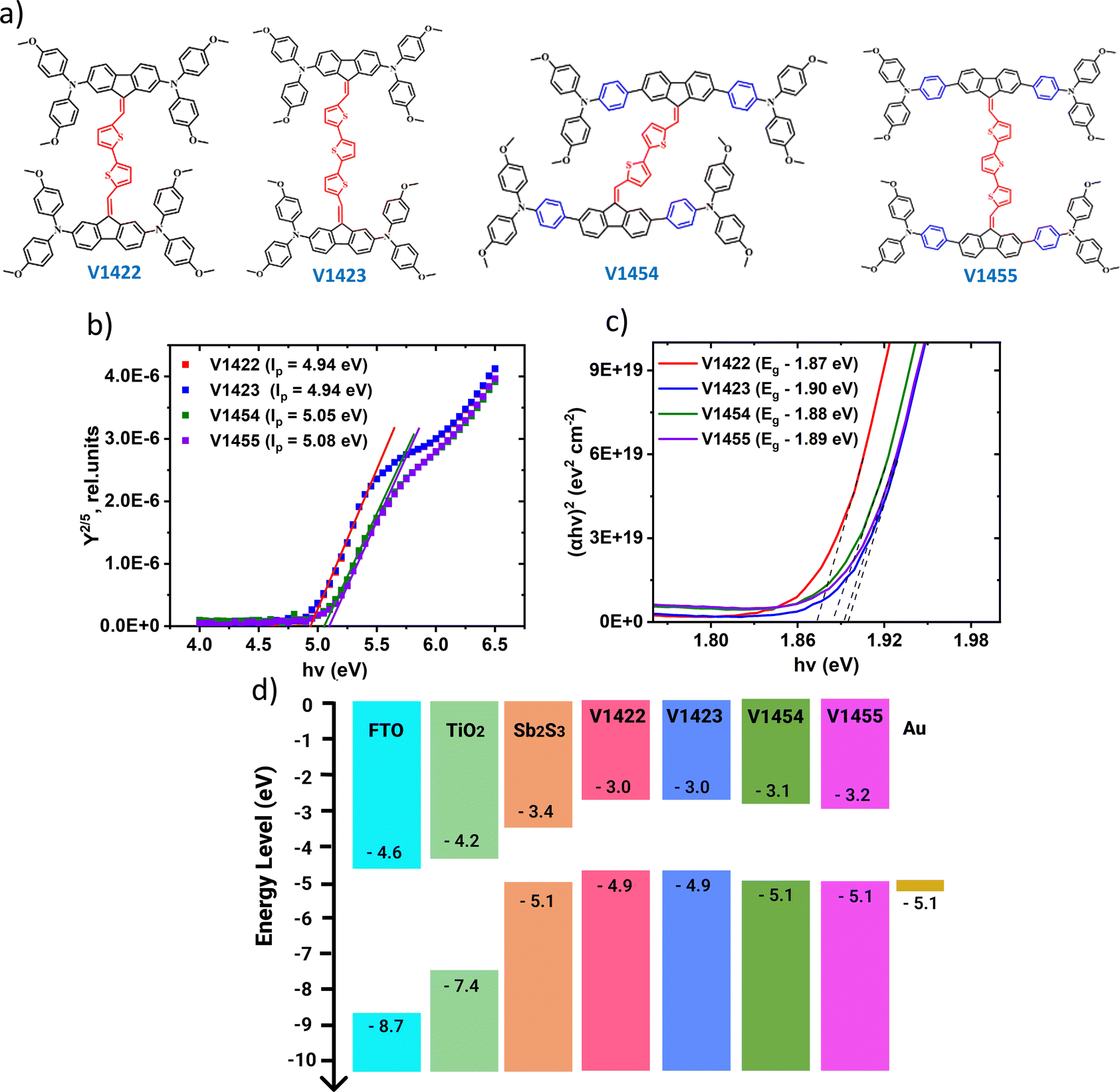 | ||
| Fig. 1 (a) Chemical structures of synthesised HTMs – V1422, V1423, V1454 and V1455, (b) ionization potential (IP), and (c) band gap (Eg) values calculated from the absorption spectra using Tauc plots for V1422, V1423, V1454 and V1455 thin films deposited on glass substrates, and (d) energy band diagram of constituent layers of the solar cell. | ||
DSC measurements indicate that thiophene linked fluorene-based dimers are molecular glasses, exhibiting glass transition temperatures (Tg) ranging from 148 °C to 175 °C (Fig. S2†), exceeding that of Spiro-OMeTAD (124 °C)26 as well as of their monomeric analogues.22 The thermal characteristics of the analysed HTMs are presented in Table 1. Comparing the Tg of new HTMs has revealed that the inclusion of triphenylamine units in HTMs' side fragments (V1454 and V1455) results in an elevated Tg. This increase could be attributed to the higher molecular mass associated with the additional triphenylamine units. It is noteworthy that V1455, with a central trithiophene-based unit and triphenylamine as side fragments, exhibits no endothermic peaks, suggesting an entirely amorphous state (Fig. S2†). This property is advantageous for the formation of homogeneous films, eliminating the potential for film crystallization during either device preparation or operation. The ultraviolet-visible (UV-Vis) absorption spectra of the HTMs (Fig. S3†) present two prominent absorption peaks at wavelengths of 300 and 375 nm, corresponding to the π–π* transitions of the side chromophores. Notably, the spectra exhibit an additional peak in the 425–550 nm range, which corresponds to π–π* transitions, and is attributed to the electron-rich thiophene π systems. Comparison of the absorption curves of molecules featuring diphenylamine units in their side fragments (V1422 and V1423) and molecules containing triphenylamine units (V1454 and V1455) has revealed that the latter show higher absorption. It can be assumed that this is due to the presence of an additional phenyl fragment in these compounds. Moreover, comparison of the absorption spectra presented in Fig. S3† with those reported for monomeric analogues in the previous study22 revealed that the number and positions of absorption peaks remain nearly unchanged, indicating that the conjugated system of the thiophene linked fluorene-based dimers is basically unaffected. As presented in Table 1, the inferred zero-field hole mobilities are 9.86 × 10⁻⁷, 1.29 × 10⁻⁶, 3.38 × 10⁻⁶, and 1.85 × 10⁻⁶ cm2 V−1 s−1 for V1422, V1423, V1454, and V1455, respectively. Therefore, it can be concluded that the presence of the additional phenyl ring in the side diphenyl units of V1454 and V1455 slightly increased the hole drift mobility.
| HTM | T g (°C) | T m (°C) | T d5 (°C) | λ abs (nm) | μ 0 (cm2 V−1 s−1) | E g (eV) | I P (eV) |
|---|---|---|---|---|---|---|---|
| V1422 | 148 | 276 | 430 | 293, 383, 468 | 9.86 × 10⁻⁷ | 1.87 | 4.94 |
| V1423 | 153 | — | 435 | 300, 383, 479 | 1.29 × 10⁻⁶ | 1.90 | 4.94 |
| V1454 | 175 | 307 | 445 | 285, 377, 467 | 3.38 × 10⁻⁶ | 1.88 | 5.05 |
| V1455 | 172 | — | 444 | 286, 377, 480 | 1.85 × 10⁻⁶ | 1.89 | 5.08 |
To understand the energy level alignment of the synthesized HTMs with that of Sb2S3 and the metal back contact, a Photoelectron Yield Spectroscopy (PYS) technique was employed for measuring the ionization potential (IP) (see Fig. 1b). The HOMO levels of V1422, V1423, V1454 and V1455 are found to be at −4.94, −4.94, −5.05 and −5.08 eV relative to the vacuum level, respectively. Thus, HTMs bearing triphenylamine units (instead of diphenylamine units) exhibit slightly lower HOMO levels. The calculated band gap (Eg) values for HTMs V1422, V1423, V1454 and V1455 thin films are 1.87, 1.90, 1.88 and 1.89 eV, respectively (see Fig. 1c). The energy band diagram is presented in Fig. 1d and reveals agreeable band offsets conducive to the photogenerated carrier transport from the absorber to the metal back contact.
The Sb2S3 absorber layer was characterized using XRD and Raman spectroscopy. Data are presented in Fig. S4, in the ESI.† The XRD results confirmed the presence of a single phase of orthorhombic Sb2S3 (ICDD PDF 01-075-4013) without any secondary phase.9,13,20,22 The Raman spectrum shows sharp peaks at 128, 155, 188, 236, 280, 302, and 312 cm−1, which are characteristic of the crystalline Sb2S3 layer.9,13,20,22 The band gap of the Sb2S3 film was 1.78 eV, as calculated from the absorption spectra using the Tauc plot (Fig. S4†), which is in line with the values previously reported for sprayed Sb2S3 films.9,13,20,21 The SEM cross-sectional images of solar cells with two HTMs, V1423 and V1454, both deposited from 2 mM solutions, are presented in Fig. S5, in the ESI.† The thickness of the Sb2S3 absorber layer was approximately 80 nm.
To study a possible chemical interaction at the Sb2S3/HTM interface, XPS studies were performed for HTMs on a glass substrate and Sb2S3 solar cell stacks without and with an HTM. The XPS spectra of Sb2S3/HTM (V1422, V1423, V1454 and V1455) samples in the Sb 3d region and S 2p region are shown in the ESI, in Fig. S6 and S7,† respectively. The Sb 3d spectra for Sb2S3 films and Sb2S3 covered with a thin layer of V1423 and V1454, are shown in Fig. 2a and b, respectively. The binding energies (BEs) of Sb 3d core level peaks in the Sb2S3 sample are located at 539.7 eV for Sb 3d3/2 and 530.3 eV for Sb 3d5/2. For the samples of Sb2S3 with V1423, the BE peak positions are shifted to lower energy values, to 539.2 eV for Sb 3d3/2 and to 529.9 eV for Sb 3d5/2.
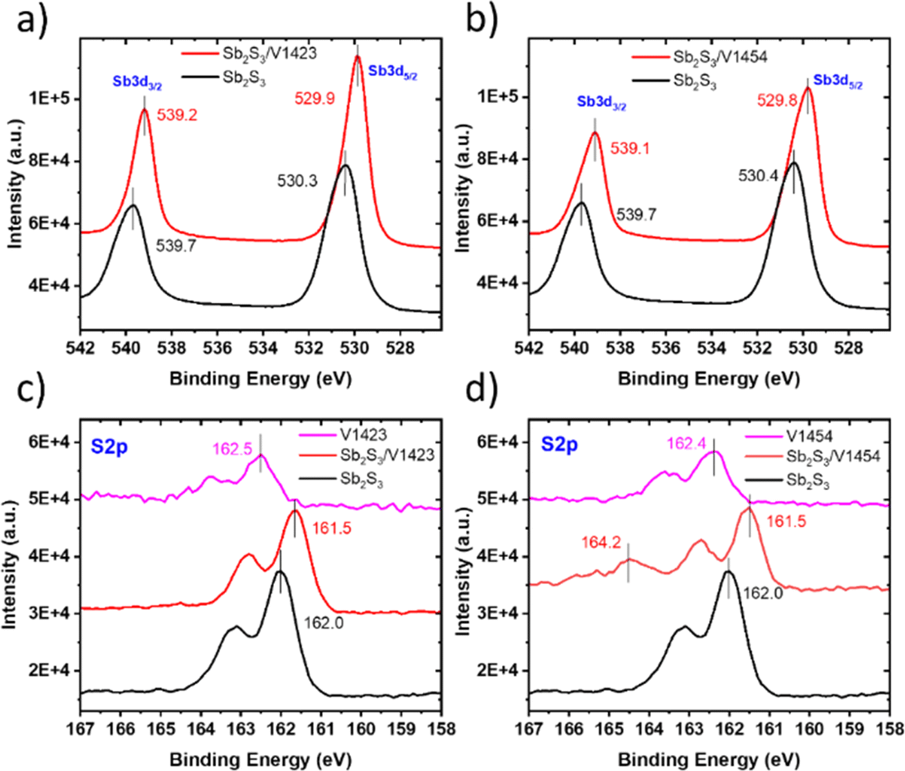 | ||
| Fig. 2 XPS core level spectra (a) Sb 3d for Sb2S3 and Sb2S3/V1423, (b) Sb 3d for Sb2S3 and Sb2S3/V1454, (c) S 2p for Sb2S3, V1423 and Sb2S3/V1423, and (d) S 2p for Sb2S3, V1454 and Sb2S3/V1454. | ||
A similar shift in Sb 3d core level peak positions to lower BE values is also observed for the sample with V1454 as the HTM (Fig. 2b). The noted shift towards lower binding energy values, in comparison to pristine Sb2S3, indicates an increased electron density around the Sb atoms in the absorber. A similar shift in the Sb 3d core level peak was observed when a dithieno[3,2-b:20,30-d]pyrrole-cored small molecule (DTPThMe-ThTPA)32 and thiophene-modified quinoxaline core small molecules27 were applied onto the Sb2(S,Se)3 film.
S 2p core level spectra for Sb2S3 films, HTMs (V1423, V1454) and Sb2S3/HTM samples are shown in Fig. 2c and d. S 2p3/2 peaks for Sb2S3 and Sb2S3/V1423 samples are positioned at BEs of 162.0 and 161.5 eV, respectively (see Fig. 2c). A similar shift of the S 2p3/2 peak towards the lower BE region is observed when V1454 is applied onto Sb2S3 (Fig. 2d). V1454 deposited onto a glass substrate shows the S 2p3/2 peak at 162.4 eV, but after deposition of V1454 onto Sb2S3 the S 2p peak of V1454 shifted to a higher energy region and peaked at a BE of 164.2 eV (see Fig. 2d and Fig. S7 in the ESI†).
A similar shift of the S 2p peak of thiophene-modified quinoxaline core small molecules to higher energies has been detected when applied to the Sb2(S,Se)3 layer.27 Interestingly, we did not detect S 2p peaks characteristic of V1423 in the spectrum of the Sb2S3/V1423 stack (Fig. 2c), although the shifts in the positions of S 2p peak and Sb 3d peak of the Sb2S3 were clearly detected upon application of V1423 onto Sb2S3. The shifts observed in Sb 3d and S 2p peak positions of Sb2S3 as well as in S 2p peak positions of HTMS refer to the interaction between S atoms from electron-rich thiophene units and Sb atoms from the Sb-chalcogenide compound which is expected to improve the interfacial carrier extraction ability.
Solar cells based on Sb2S3 were prepared in the superstrate configuration glass/FTO/TiO2/Sb2S3/HTM/Au (see the sketch in Fig. 3a and SEM images in Fig. S5, in the ESI†). The systematic change in the concentration of V-series HTM solutions (4, 2, 1, 0.6 mM) was studied. The resulting output parameters are presented in Table S1, in the ESI.† Solar cells fabricated with 2 mM solutions showed the highest performance, independent of the HTM used. The current–voltage (J–V) characteristics of the best performing devices using 2 mM HTM solutions are presented in Fig. 3b, and the cell output parameters are summarized in Table 2. The reference device, lacking an HTM, yielded a VOC of 478 mV, JSC of 8.7 mA cm−2, FF of 0.46, and a PCE of 1.9%. Introduction of V1422 and V1423 as HTMs resulted in open circuit voltages of 656 and 673 mV, respectively. On application of HTMs, also other solar cell parameters improved as compared to the cells without an HTM. In the case of the cell with V1423, JSC improved from 9.0 to 12.1 mA cm−2, FF from 0.46 to 0.56 and PCE from 1.9 to 4.5%. Therefore, the utilization of HTMs – V1422 and V1423 substantially mitigates carrier recombination at the back interface, leading to improved carrier collection. Notably, the device with the HTM – V1423 yielded device output characteristics comparable to those employing P3HT. In contrast, solar cell devices with V1454 and V1455, having triphenylamine side fragments, yielded VOC values of 439 and 437 mV, respectively. As compared to the solar cell without any HTM, there was no improvement in VOC values. In addition, an increase in series resistance (RS) values and a decrease in JSC, FF and overall PCE was recorded (Fig. 3b and Table 2). High RS values up to ca. 5 Ω cm2 in solar cells could result from an excessively thick layer. For the purpose of reducing the HTM layer thickness, solar cells were fabricated with diluted HTM solutions. The concentration of HTM solutions was decreased from 2 mM to 0.6 mM. However, no notable improvement in solar cell parameters was observed, as detailed in the ESI, Table S1.† The external quantum efficiency (EQE) graphs of the champion devices without any HTM and with different HTM layers are presented in Fig. 3c. It should be noted that the integrated JSC, calculated based on EQE spectra, closely correspond to the values obtained from the J–V curves (see Table 2). A dip in the spectral response in the case of the device with P3HT can be seen in the range of 550–650 nm, which is attributed to its parasitic absorption losses.20,22 Normalized EQE curves of the devices with investigated HTMs are presented in the ESI, in Fig. S9.† The concavity in the EQE curve is less pronounced in the case of samples with V-series HTMs. All investigated HTMs have a similar band gap, within the range of 1.8–1.9 eV. However, the V-series HTM layers were considerably thinner, approximately 20–25 nm, in contrast to P3HT, with a thickness of about 80–100 nm. Thus, devices with V-series HTMs show an average visible transmittance (AVT) of 24–26% compared to 21% by the P3HT-based device (see Fig. S10 in the ESI†). A statistical representation (i.e., box plots) of solar cell parameters of the fabricated cells without any HTM and with investigated HTMs (Fig. 3d–i) refers to high reproducibility of the results.
 | ||
| Fig. 3 (a) Schematic of the Sb2S3 absorber solar cell (glass/FTO/TiO2/Sb2S3/HTM/Au) fabricated in the superstrate configuration, (b) J–V characteristics, (c) external quantum efficiency (EQE) curves with the calculated integrated JSC curves of the champion solar cells without (w/o) the HTM and with different HTMs (P3HT, V1422, V1423, V1454 and V1455). Box plots of Sb2S3 solar cells without any HTM (Sb2S3/Au) and with P3HT, V1422, V1423, V1454 and V1455 as HTMs: (d) VOC, (e) JSC, (f) fill factor (FF), (g) PCE, (h) series resistance (RS), and (i) shunt resistance (RSH). | ||
| HTM | HTM conc. (mg mL−1) | V OC (mV) | J SC (mA cm−2) | Integrated JSC (mA cm−2) | FF (%) | PCE (%) | R S (Ω cm2) | R SH (Ω cm2) |
|---|---|---|---|---|---|---|---|---|
| w/o | — | 478 | 8.7 | 9.0 | 46 | 1.9 | 1.1 | 514 |
| V1422 | 2 mM | 656 | 9.7 | 9.9 | 43 | 3.9 | 1.7 | 436 |
| V1423 | 2 mM | 673 | 12.1 | 12.0 | 56 | 4.5 | 1.3 | 1005 |
| V1454 | 2 mM | 439 | 5.7 | 6.8 | 35 | 0.8 | 2.7 | 192 |
| V1455 | 2 mM | 437 | 6.1 | 7.1 | 33 | 0.7 | 4.9 | 198 |
| P3HT | 1 wt% | 689 | 12.2 | 12.2 | 55 | 4.7 | 1.8 | 526 |
Although the interaction between the S atom from the thiophene unit and Sb from Sb2S3 has been noted in all interfaces with V-series HTMs, only the use of V1422 and V1423 as HTMs led to an increase in the open-circuit voltage (VOC) of up to 650–670 mV. Furthermore, only the application of V1423 in the solar cell structure resulted in fill factor values of up to 56%, leading to conversion efficiencies exceeding 4% (see box-plot, in Fig. 3), which is very close to that obtained using P3HT as the HTM. Our results show that V1423, a dimer molecule with three thiophene units in its structure is the most efficient one in this family of novel HTMs. The application of V1454 and V1455 as HTM layers did not reduce the interface recombination or improve the carrier collection. VOC remains on the level of 400 mV comparable to the cells without the HTM, fill factor values are low and vary in the region 30–35%. The current density is ca. two times lower as compared to the cell with V1423 and the solar cell exhibits a high RS value of ca. 5 Ω cm2 (Fig. 3d–i). Consequently, the solar cell conversion efficiencies are below 1%, that is two times lower than that recorded for the cells without any HTM.
As stated above, the interaction of S from the thiophene unit with Sb from Sb2S3 at the absorber surface may explain the improvement of the VOC and overall solar cell parameters via passivation of the interfacial states. Although such a mechanism is validated by the enhanced VOC in V1422 and V1423-based devices, the abrupt decrease in the VOC and overall performance of V1454 and V1455-based cells indicate that there might be another concomitant phenomenon which prevails or compensates the benefit of thiophene-based interactions. A possible explanation for the low VOC and PCE of V1454 and V1455-based cells, can be linked to the dipole effects at the absorber/HTM interface. As demonstrated in organic solar cells, insertion of organic materials between the photoactive absorber layer and electrodes can be an efficient approach for manipulation of the electric potential distribution by dipole moments at the electrode surface.33–35 Several experimental and numerical simulation studies reported that the dipoles at the back/front interfaces have to be aligned in such a way that it allows accumulation of high hole concentration at the vicinity of hole contact and high electron density at the vicinity of electron contact.33,36 The efficiency of photogenerated charge carrier separation (and thus, improved charge selectivity) is influenced by the specific arrangement of the molecules and the orientation of the permanent dipole moment. Thus, in some cases, depending on the angular configuration and molecular arrangement, the organic molecules can act as hole or electron selective layers. For example, Kippelen et al., demonstrated that the HTM – PEDOT:PSS can be easily altered to a well-functionalized electron transport layer by complexation with polyethylenimine ethoxylated (PEIE) molecules.37
Considering these approaches, it can be assumed that in V1454 and V1455 based solar cell devices, the additional phenyl fragment in the HTMs reconfigured the angular and molecular arrangement resulting in unsuitable alignment in the orientation of the dipoles at the back interface. As a consequence, this imposes an increase of an “incorrect” type of charge carrier concentration in the vicinity of the metal back contact (i.e., electron proximity of the Hall contact), decreasing the VOC and deteriorating the overall device performance. Validation of this hypothesis can be assured by in-depth analysis of the changes in the work function of the contact electrode in proximity of the HTM. This approach would imply complex correlative measurements of Kelvin-probe AFM and UPS combined with numerical simulations which has been applied in organic solar cells33 and remains a great challenge for the emerging Sb2S3/HTM interface.
The anomalous low performance of V1454 and V1455-based cells can be approached from a different angle – by analysing the molecular geometry and orbitals and correspondingly, the positions of the Highest Occupied Molecular Orbital (HOMO) and Lowest Unoccupied Molecular Orbital (LUMO) of V1422 (a representative of molecules with diphenylamine units in their structures) and V1454 (a representative of molecules with triphenylamine units in their structures) from quantum chemical simulation. Fig. 4 presents the optimized geometry of HTM compound molecules of V1422 and V1454, and their HOMO and LUMO.
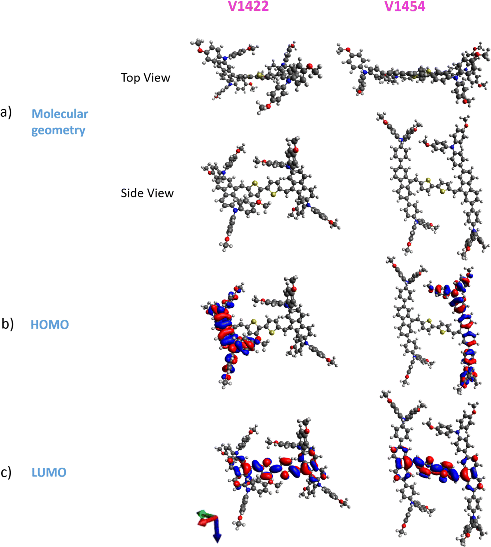 | ||
| Fig. 4 (a) Optimized geometry of HTM molecules – V1422 and V1454 in top and side views, (b) highest occupied molecular orbital (HOMO) in HTMs – V1422 (left) and V1454 (right), (c) lowest unoccupied molecular orbital (LUMO) in HTMs – V1422 (left) and V1454 (right). Colors used for atoms: gray – C, white – H, yellow – S, red – O and blue – N. | ||
The result of the simulation shows that HOMO levels of both V1454 and V1422 are formed by fluorene and benzene rings, while LUMO is primarily located on the thiophene groups. In addition to this HOMO–LUMO configuration, compared to V1422 (having a nonplanar orientation of fluorene in relation to the thiophene groups), V1454 exhibits more planar arrangement of fluorene groups relative to the thiophene groups. The latter effect allows a greater accessibility of the thiophene moieties in V1454 and consequently, a stronger interaction between S atoms in the thiophene group and Sb from Sb2S3. This strong interaction is highlighted by the observed shift of the V1454 S 2p3/2 peak towards the higher BE region when applied onto Sb2S3 (Fig. 2d, XPS analysis). However, this strong interaction does not result in an improved charge carrier transport through the interface since the HOMO level is not located on thiophene moieties and thus the condition for the accumulation of the “right” type of charge carrier (i.e., holes) at the back interface is not satisfied. Thus, the quantum chemical simulation results suggest that to achieve higher efficiency of photogenerated charge carrier separation and improved charge selectivity by an organic HTM layer, the HOMO of the HTMs should be formed by the thiophene groups. Although this hypothesis may interfere with other requirements for the alignment of the electronic states at the organic/inorganic interfaces, these results lay a solid foundation for further investigations and understanding the charge transfer kinetics at the Sb2S3/HTM interface.
4. Conclusion
Four dopant-free dimers (V1422, V1423, V1454, V1455) comprising methoxydiphenylamine substituted fluorene derivatives and connected by central cores consisting of different numbers of thiophene moieties were synthesized by a solution chemical route. Synthesized organic semiconductors are molecular glasses, exhibiting glass transition and thermal decomposition temperatures of 148–175 °C and 430–445 °C, respectively and having an energy band gap of 1.9 eV and ionization potential of 4.9–5.1 eV. Synthesized organic semiconductors were explored, for the first time, as HTMs in superstrate configuration FTO/TiO2/Sb2S3/HTM/Au solar cells in which the Sb2S3 absorber and TiO2 layers were deposited by the ultrasonic spray method while HTM layers were obtained by spin-coating. Energy level diagrams demonstrate agreeable band offsets validating the applicability of the synthesized materials as efficient HTMs in an FTO/TiO2/Sb2S3/HTM/Au device. It has been shown that application of the HTM layer on top of the Sb2S3 layer induces a shift in the Sb 3d core level peak to lower binding energies, indicating increased electron density surrounding the Sb atoms. Such a shift confirms the interaction between S atoms from thiophene units and Sb atoms from the absorber occurring at the Sb2S3/HTM interface. By introducing HTMs comprising diphenylamine units in their structures (V1422, V1423) into the solar cell structure, an increase in the device output characteristics compared to the device without an HTM layer was observed. The highest boost in device performance was observed for V1423-based cells, exhibiting an increase of the VOC from 478 mV to 673 mV, fill factor from 46% to 56%, and PCE from 1.9% to 4.5%.Thus, it can be concluded that this type of HTM effectively mitigates carrier recombination at the back interface, and contributes to better collection of carriers. The application of V1454 and V1455 (molecules with triphenylamine units in their structures) as HTM layers did not improve the device parameters as the VOC remained on the level of 430 mV (comparable to the cells without HTMs) while the fill factor values reached the lowest level of 30–35%. For the same cells, the JSC values were two times lower compared to the cells with V1423 and the PCEs of solar cells were below 1% – two times lower than those recorded for the cells without any HTM. The abrupt decrease in the VOC, JSC and overall performance of V1454 and V1455-based cells indicates the presence of a concomitant phenomenon which prevails or compensates the benefit of thiophene-based interactions. Possible phenomena occurring at the Sb2S3/HTM interface were discussed through the prism of correlation between the efficiency of the charge transfer/charger selectivity and final device performance, including possible impacts of the dipole effect as well as a prospective analysis from the quantum chemical simulation side. The results of quantum chemical simulation suggest that to achieve higher efficiency of photogenerated charge carrier separation and improved charge selectivity by the organic HTM layer, the HOMO of the HTMs should be configured by the thiophene groups. So far, the results of this study provide new perspectives on the chemical and physical understanding of Sb2S3/HTM organic/inorganic interfaces towards the identification of suitable innovative HTMs which would allow a significant boost in the efficiency of the emerging Sb-chalcogenide thin film PV technology.
Data availability
The data that support the findings of this study will be made available by the corresponding author upon request.Author contributions
Nimish Juneja – conceptualization, methodology, validation, data curation, writing – original draft. Aistė Jegorovė – conceptualization, methodology, validation, writing – review & editing. Raitis Grzibovskis – methodology, validation, writing – review & editing. Atanas Katerski – methodology, validation. Maryte Daskeviciene – writing – review & editing. Tadas Malinauskas – writing – review & editing. Aivars Vembris – conceptualization, methodology, validation, writing – review & editing. Smagul Karazhanov – writing – review & editing. Nicolae Spalatu – methodology, formal analysis, visualization, supervision, writing – review & editing. Vytautas Getautis – conceptualization, methodology, validation, writing – review & editing. Malle Krunks – conceptualization, methodology, validation, supervision, writing – review & editing. Ilona Oja Acik – conceptualization, funding acquisition, project administration, writing – review & editing.Conflicts of interest
There are no conflicts to declare.Acknowledgements
The “Development of Semi-Transparent Bifacial Thin Film Solar Cells for Innovative Applications” benefits from a 999372 € grant from Iceland, Liechtenstein and Norway through the EEA Grants. The aim of the project is to develop a new approach based on novel materials and structures and production technologies, which are the key to further increasing the share, and range of application of PV in areas with sub-average sunlight, including Baltic and Nordic countries. Therefore, development of resource saving, cost-effective and efficient PV devices is a primary challenge of this project. The project contract no. with the Research Council of Lithuania (LMTLT) is S-BMT-21-1 (LT08-2-LMT-K-01-003). Department of Materials and Environmental Technology, Tallinn University of Technology has received funding from the Estonian Research Council, projects PRG627 “Antimony Chalcogenide Thin films for Next-Generation Semi-transparent Solar Cells Applicable in Electricity Producing Windows” and PSG689 “Bismuth Chalcogenide Thin-Film Disruptive Green Solar Technology for Next Generation Photovoltaics”. The research was partially funded by the European Union's Horizon 2020 ERA Chair project 5GSOLAR (grant agreement no. 952509). The research was supported by the European Cooperation in Science and Technology (COST) project RENEW-PV (CA21148) and by the Estonian Ministry of Education and Research (project TK210; TK210U8 “Center of Excellence in Sustainable Green Hydrogen and Energy Technologies”). Institute of Solid-State Physics, University of Latvia has received funding from the European Union's Horizon 2020 Framework Programme H2020-WIDESPREAD-01-2016-2017-TeamingPhase2 under grant agreement no. 739508, project CAMART2.Notes and references
- N. Cates and M. Bernechea, APL Mater., 2018, 6, 084503 CrossRef
.
- S. Barthwal, R. Kumar and S. Pathak, ACS Appl. Energy Mater., 2022, 5, 6545–6585 CrossRef CAS
- M. Koltsov, S. V. Gopi, T. Raadik, J. Krustok, R. Josepson, R. Gržibovskis, A. Vembris and N. Spalatu, Sol. Energy Mater. Sol. Cells, 2023, 254, 112292 CrossRef CAS
- C. Comparotto, P. Ström, O. Donzel-Gargand, T. Kubart and J. J. S. Scragg, ACS Appl. Energy Mater., 2022, 5, 6335–6343 CrossRef CAS
- S. Wang, Y. Zhao, B. Che, C. Li, X. Chen, R. Tang, J. Gong, X. Wang, G. Chen, T. Chen, J. Li and X. Xiao, Adv. Mater., 2022, 34, 2206242 CrossRef CAS PubMed
- Y. Zhao, S. Wang, C. Li, B. Che, X. Chen, H. Chen, R. Tang, X. Wang, G. Chen, T. Wang, J. Gong, T. Chen, X. Xiao and J. Li, Energy Environ. Sci., 2022, 15, 5118–5128 RSC
- Y. Zhao, S. Wang, C. Jiang, C. Li, P. Xiao, R. Tang, J. Gong, G. Chen, T. Chen, J. Li and X. Xiao, Adv. Energy Mater., 2022, 12, 2103015 CrossRef CAS
- A. A. F. Husain, W. Z. W. Hasan, S. Shafie, M. N. Hamidon and S. S. Pandey, Renewable Sustainable Energy Rev., 2018, 94, 779–791 CrossRef CAS
- J. S. Eensalu, A. Katerski, E. Kärber, L. Weinhardt, M. Blum, C. Heske, W. Yang, I. Oja Acik and M. Krunks, Beilstein J. Nanotechnol., 2019, 10, 2396–2409 CrossRef CAS PubMed
- V. K. H. Bui and T. P. Nguyen, Polymers, 2023, 15, 4443 CrossRef CAS PubMed
- E. Zimmermann, T. Pfadler, J. Kalb, J. A. Dorman, D. Sommer, G. Hahn, J. Weickert and L. Schmidt-Mende, Adv. Sci., 2015, 2, 1500059 CrossRef PubMed
- M. S. You, C.-S. Lim, D. H. Kwon, J. H. Heo, S. H. Im and K. J. Chae, Org. Electron., 2015, 21, 155–159 CrossRef CAS
- J. S. Eensalu, A. Katerski, E. Kärber, I. Oja Acik, A. Mere and M. Krunks, Beilstein J. Nanotechnol., 2019, 10, 198–210 CrossRef PubMed
- J. Chen, J. Qi, R. Liu, X. Zhu, Z. Wan, Q. Zhao, S. Tao, C. Dong, G. Y. Ashebir, W. Chen, R. Peng, F. Zhang, S. Yang, X. Tian and M. Wang, Commun. Chem., 2019, 2, 121 CrossRef
- Y. Zhang, S. Li, R. Tang, X. Wang, C. Chen, W. Lian, C. Zhu and T. Chen, Energy Technol., 2018, 6, 2126–2131 CrossRef CAS
- Y. Yang, C. Shi, K. Lv, Q. Wang, X. Sun and W. Chen, New J. Chem., 2021, 45, 10357–10361 RSC
- X. Jin, Y. Fang, T. Salim, M. Feng, Z. Yuan, S. Hadke, T. C. Sum and L. H. Wong, Adv. Mater., 2021, 33, 2104346 CrossRef CAS PubMed
- R. Tang, X. Wang, W. Lian, J. Huang, Q. Wei, M. Huang, Y. Yin, C. Jiang, S. Yang, G. Xing, S. Chen, C. Zhu, X. Hao, M. A. Green and T. Chen, Nat. Energy, 2020, 5, 587–595 CrossRef CAS
- M. L. Petrus, T. Bein, T. J. Dingemans and P. Docampo, J. Mater. Chem. A, 2015, 3, 12159–12162 RSC
- N. Juneja, S. Mandati, A. Katerski, N. Spalatu, S. Daskeviciute-Geguziene, A. Vembris, S. Karazhanov, V. Getautis, M. Krunks and I. Oja Acik, Sustainable Energy Fuels, 2022, 6, 3220–3229 RSC
- N. Juneja, S. Daskeviciute-Geguziene, N. Spalatu, S. Mandati, A. Katerski, R. Grzibovskis, A. Vembris, S. Karazhanov, V. Getautis, M. Krunks and I. Oja Acik, Mater. Sci. Semicond. Process., 2024, 169, 107934 CrossRef CAS
- S. Mandati, N. Juneja, A. Katerski, A. Jegorovė, R. Grzibovskis, A. Vembris, T. Dedova, N. Spalatu, A. Magomedov, S. Karazhanov, V. Getautis, M. Krunks and I. Oja Acik, ACS Appl. Energy Mater., 2023, 6, 3822–3833 CrossRef CAS PubMed
- D. Poplavskyy and J. Nelson, J. Appl. Phys., 2003, 93, 341–346 CrossRef CAS
- S.-J. Moon, Y. Itzhaik, J.-H. Yum, S. M. Zakeeruddin, G. Hodes and M. Grätzel, J. Phys. Chem. Lett., 2010, 1, 1524–1527 CrossRef CAS
- S. Daskeviciute, C. Momblona, K. Rakstys, A. A. Sutanto, M. Daskeviciene, V. Jankauskas, A. Gruodis, G. Bubniene, V. Getautis and M. K. Nazeeruddin, J. Mater. Chem. A, 2021, 9, 301–309 RSC
- T. Malinauskas, D. Tomkute-Luksiene, R. Sens, M. Daskeviciene, R. Send, H. Wonneberger, V. Jankauskas, I. Bruder and V. Getautis, ACS Appl. Mater. Interfaces, 2015, 7, 11107–11116 CrossRef CAS PubMed
- Y. Xiang, H. Guo, Z. Cai, C. Jiang, C. Zhu, Y. Wu, W.-H. Zhu and T. Chen, Chem. Commun., 2022, 58, 4787–4790 RSC
- S. Xu, J. Wu, F. Guo, M. Wu, S. Chen, W. Chen and C. Shi, Sustainable Energy Fuels, 2023, 7, 61–65 RSC
- S. H. Im, C.-S. Lim, J. A. Chang, Y. H. Lee, N. Maiti, H.-J. Kim, M. K. Nazeeruddin, M. Grätzel and S. Il Seok, Nano Lett., 2011, 11, 4789–4793 CrossRef CAS PubMed
-
M. J. Frisch, G. W. Trucks, H. B. Schlegel, G. E. Scuseria, M. A. Robb, J. R. Cheeseman, G. Scalmani, V. Barone, G. A. Petersson and H. Nakatsuji, Gaussian 09, Revision A.02, Gaussian Inc., Wallingford CT, 2016 Search PubMed
- M. V. Khenkin, E. A. Katz, A. Abate, G. Bardizza, J. J. Berry, C. Brabec, F. Brunetti, V. Bulović, Q. Burlingame, A. Di Carlo, R. Cheacharoen, Y.-B. Cheng, A. Colsmann, S. Cros, K. Domanski, M. Dusza, C. J. Fell, S. R. Forrest, Y. Galagan, D. Di Girolamo, M. Grätzel, A. Hagfeldt, E. von Hauff, H. Hoppe, J. Kettle, H. Köbler, M. S. Leite, S. Liu, Y.-L. Loo, J. M. Luther, C.-Q. Ma, M. Madsen, M. Manceau, M. Matheron, M. McGehee, R. Meitzner, M. K. Nazeeruddin, A. F. Nogueira, Ç. Odabaşı, A. Osherov, N.-G. Park, M. O. Reese, F. De Rossi, M. Saliba, U. S. Schubert, H. J. Snaith, S. D. Stranks, W. Tress, P. A. Troshin, V. Turkovic, S. Veenstra, I. Visoly-Fisher, A. Walsh, T. Watson, H. Xie, R. Yıldırım, S. M. Zakeeruddin, K. Zhu and M. Lira-Cantu, Nat. Energy, 2020, 5, 35–49 CrossRef
- C. Jiang, J. Zhou, R. Tang, W. Lian, X. Wang, X. Lei, H. Zeng, C. Zhu, W. Tang and T. Chen, Energy Environ. Sci., 2021, 14, 359–364 RSC
- U. Würfel, M. Seßler, M. Unmüssig, N. Hofmann, M. List, E. Mankel, T. Mayer, G. Reiter, J. Bubendorff, L. Simon and M. Kohlstädt, Adv. Energy Mater., 2016, 1600594 CrossRef
- J. Kesters, T. Ghoos, H. Penxten, J. Drijkoningen, T. Vangerven, D. M. Lyons, B. Verreet, T. Aernouts, L. Lutsen, D. Vanderzande, J. Manca and W. Maes, Adv. Energy Mater., 2013, 3, 1180–1185 CrossRef CAS
- F. A. Nüesch, Chimia, 2013, 67, 388–392 CrossRef PubMed
- C. F. N. Marchiori and M. Koehler, J. Phys. D Appl. Phys., 2014, 47, 215104 CrossRef
- Y. Zhou, C. Fuentes-Hernandez, J. Shim, J. Meyer, A. J. Giordano, H. Li, P. Winget, T. Papadopoulos, H. Cheun, J. Kim, M. Fenoll, A. Dindar, W. Haske, E. Najafabadi, T. M. Khan, H. Sojoudi, S. Barlow, S. Graham, J.-L. Brédas, S. R. Marder, A. Kahn and B. Kippelen, Science, 2012, 336, 327–332 CrossRef CAS PubMed
Footnote |
| † Electronic supplementary information (ESI) available. See DOI: https://doi.org/10.1039/d4se00472h |
| This journal is © The Royal Society of Chemistry 2024 |