 Open Access Article
An ambient process for hole transport layer-free highly stable MAPbI3 by addition of MACl for efficient perovskite solar cells†
Pardhasaradhi
Nandigana
 ab,
Bavatharini
Saminathan
a,
Sriram
P.
ab,
Sujatha
D.
ab,
Imthiaz Ahmed
M.
a,
Ram Prasanth
R.
a,
B.
Subramanian
ab and
Subhendu K.
Panda
ab,
Bavatharini
Saminathan
a,
Sriram
P.
ab,
Sujatha
D.
ab,
Imthiaz Ahmed
M.
a,
Ram Prasanth
R.
a,
B.
Subramanian
ab and
Subhendu K.
Panda
 *ab
*ab
aEMF Division, CSIR – Central Electrochemical Research Institute, Karaikudi, Tamil Nadu 630003, India. E-mail: skpanda@cecri.res.in; Tel: +91 4565 241234
bAcademy of Scientific and Innovative Research (AcSIR), Ghaziabad-201002, India
First published on 2nd January 2024
Abstract
Methylammonium lead iodide (MAPbI3) is a front-runner material for efficient perovskite solar cells (PSCs) due to its high light-absorption coefficient, suitable bandgap, and superior charge carrier mobility. However, high-quality photoactive MAPbI3 (MAPI) perovskite thin-films are usually fabricated in controlled atmospheric conditions (inside a glove box) and annealed at high temperature (generally >120 °C for 20 min). Here, we report a facile method to fabricate high quality MAPbI3 (MAPI) thin-films by the simple addition of an MA-based volatile additive, i.e., methylammonium chloride (MACl). The optimized amount of MACl in the perovskite solution produced a highly crystalline and optically active MAPI black perovskite phase at room temperature under ambient atmospheric conditions. MACl not only regulates the surface morphology of the perovskite films, but also the intermediate phases by altering the formation energy of the perovskite material. MACl lowered the formation energy of the MAPI perovskite resulting in the room temperature formation of phase pure MAPI perovskite under ambient conditions. Finally, we assembled perovskite solar cell devices with an HTL-free carbon-based architecture to determine the photovoltaic performance of the prepared thin-films. Our champion device showed a power conversion efficiency as high as 7.11% with an open circuit voltage of 0.98 V, short circuit current density of 11.03 mA cm−2 and a fill-factor of 65.86%. The device was stable over 10 days under ambient conditions and retained ∼80% of its initial efficiency. These results are favourable for large-scale fabrication to make it commercially viable.
Introduction
In recent years, hybrid organic–inorganic metal halide perovskites (AMX3: A = organic cation, M: Pb and X: halide (I, Br, Cl)) have gained great attention due to their excellent optoelectronic properties, such as high charge carrier mobility, tunable band gap, small exciton binding energy, long carrier diffusion length, and high absorption coefficients.1–4 Miyasaka and co-workers utilized perovskite (MAPbI3/MAPbBr3) nanocrystals as a light absorber material in dye sensitized solar cells (DSSCs) for the first time and reported that the power conversion efficiency (PCE) was about 3.8% in 2009.5 In 2012, Park and Gratzel et al. introduced a solid hole transport layer in perovskite solar cells to enhance the stability and performance of the device.6 The power conversion efficiency (PCE) of single junction perovskite solar cells (PSCs) has been increased to over 25.7% surpassing the record of conventional silicon-based solar cells.7 Currently, most of the perovskite solar cell fabrication is confined to a controlled atmosphere (N2/Ar filled glove box) and annealing at high temperatures such as 130 °C to 150 °C to form the perovskite phase. These conditions will limit the production of perovskite solar cells on an industrial scale. It's necessary to fabricate the solar cell devices under ambient conditions at room temperature to make it commercially viable. Wan-Jian Yin et al. reported a dramatic decrease in the formation temperature of CsPbI3 perovskite thin-films by the incorporation of small amounts of bromide.8 Similarly, Dianyi Liu and co-workers continued this work and fabricated CsPbI2Br perovskite thin-films at room temperature showing a PCE of 8.67% for flexible inverted PSCs.9 Maryam Bari and co-workers reported room temperature grown MAPbX3 (X = I, Br, Cl) single crystals by creating constant supersaturation during the crystal growth and obtained large single crystals at room temperature via controlled solvent evaporation and studied their optical properties.10 Lixiu Zhang et al. reported room temperature formation of MAPI perovskite thin-films by using a low boiling point solvent and obtained a PCE of 18.21%.11 Zijiang Yang and co-workers developed a novel strategy to produce the room temperature formation of phase pure MAPI perovskite thin-films via anti-solvent (chloroform) washing and reported a PCE as high as 17.7% under ambient conditions with a relative humidity of about 30% at room temperature.12 To form a highly crystalline iodide or iodide/bromide perovskite and attain high performance in PSCs, sources containing only iodide and bromide salts (such as PbI2, PbBr2, MAI, FAI, CsI, MABr) are typically used as precursors. However, recently, MACl as an excellent additive to regulate the perovskite crystallization, giving uniform film formation (full coverage over all the surface of the perovskite thin-film) and defect passivation at grain boundaries in the presence of MACl, has been widely explored.13–15 Zhu et al. introduced MACl in the bulk MAPI perovskites for the first time and studied their crystal structure, charge carrier dynamics and performance of PSCs. They observed better film formation and improved recombination resistance in planar perovskites, which results in an enhanced PCE from 2% to 12%.15 Besides, there are different ways to introduce MACl effectively into the bulk perovskites, such as one-step conventional spin-coating, one-step spin-coating under iodide-deficient conditions, two-step conversion, and post-treatment of the perovskite film with MACl.16–19 Among these routes, a single step deposition process, i.e. addition of an excess amount of MACl to the 1![[thin space (1/6-em)]](https://www.rsc.org/images/entities/char_2009.gif) :
:![[thin space (1/6-em)]](https://www.rsc.org/images/entities/char_2009.gif) 1 ratio of MAI and PbI2 resulted in higher crystallinity, and good morphology with higher grain size and entire surface coverage without pinholes on the perovskite thin-films was observed, which resulted in enhanced performance of the PSC with negligible hysteresis.
1 ratio of MAI and PbI2 resulted in higher crystallinity, and good morphology with higher grain size and entire surface coverage without pinholes on the perovskite thin-films was observed, which resulted in enhanced performance of the PSC with negligible hysteresis.
It is important to mention that MACl not only regulates the surface morphology of the perovskite films, but also regulates the intermediate phases of the perovskite material at the time of deposition. Kim and co-workers investigated the effect of MACl on the perovskites (FAPbI3) experimentally as well as theoretically. MACl successfully induces the intermediate phase of pure α-FAPbI3 at room temperature. Furthermore, the formation energy of the bulk perovskite varies with the concentration of MACl incorporated into the perovskite solution.20 The formation energy of MAPI is less than that of FAPbI3 because the ionic radius of the MA cation is less than that of the FA cation. In this work, we are incorporating an optimized amount of MACl into the MAPI perovskite solution (PbI2![[thin space (1/6-em)]](https://www.rsc.org/images/entities/char_2009.gif) :
:![[thin space (1/6-em)]](https://www.rsc.org/images/entities/char_2009.gif) MAI with 1
MAI with 1![[thin space (1/6-em)]](https://www.rsc.org/images/entities/char_2009.gif) :
:![[thin space (1/6-em)]](https://www.rsc.org/images/entities/char_2009.gif) 1) for room temperature formation of phase pure semiconductor grade MAPI perovskite films. MACl modified MAPI films showed high crystallinity, improved surface morphology with larger grain sizes and improved optoelectronic properties at room temperature under ambient conditions. To promote commercialization, lowering the production cost and reducing the complexity of the process would make the devices more competitive and thus are highly required. In this respect, we assembled perovskite solar cell devices with a HTL-free carbon-based device architecture (FTO/c-TiO2/mp-TiO2/perovskite/carbon) and studied their photovoltaic properties and stability under ambient atmospheric conditions.
1) for room temperature formation of phase pure semiconductor grade MAPI perovskite films. MACl modified MAPI films showed high crystallinity, improved surface morphology with larger grain sizes and improved optoelectronic properties at room temperature under ambient conditions. To promote commercialization, lowering the production cost and reducing the complexity of the process would make the devices more competitive and thus are highly required. In this respect, we assembled perovskite solar cell devices with a HTL-free carbon-based device architecture (FTO/c-TiO2/mp-TiO2/perovskite/carbon) and studied their photovoltaic properties and stability under ambient atmospheric conditions.
Experimental section
Materials
Methylammonium iodide (MAI) (99.0%), lead iodide (PbI2) (99.99%), and methylammonium chloride (MACl) (98.0%) were purchased from TCI chemicals. Chlorobenzene (Extra Pure), DMF (99%) and DMSO (99.9%) were purchased from Alfa Aesar. Titanium oxide nanoparticles (P-25) (99.5%), titanium(IV) isopropoxide (98%), conductive carbon paste and FTO glass substrates (7 Ω sq−1) were purchased from Sigma Aldrich. Absolute ethanol (100%, Hayman ethanol) was used. All the chemicals were used without further purification.Perovskite thin-film fabrication
Perovskite solution was prepared by mixing equimolar (1.3 M) amounts of MAI and PbI2 in DMF and DMSO mixed solvent (7![[thin space (1/6-em)]](https://www.rsc.org/images/entities/char_2009.gif) :
:![[thin space (1/6-em)]](https://www.rsc.org/images/entities/char_2009.gif) 3) and stirred overnight. The obtained clear perovskite solution was used for spin coating. Then the perovskite thin-films were prepared by spin coating by a two-step spin coating process. Initially, 40 μL of the perovskite solution was drop cast onto FTO and spin coated at 1000 rpm for 10 s, followed by 5000 rpm for 30 s. During the second step, the anti-solvent chlorobenzene was dropped 10 s before completion. Pristine perovskite thin-films without annealing were named as MAPI_RT, and the films annealed at 120 °C were named as MAPI_120 °C. Furthermore, to understand the effect of MACl, different amounts, such as 0.1 M, 0.2 M and 0.3 M of MACl were added to the pristine perovskite solutions and stirred for 6 h at room temperature under ambient conditions. The thin-films are fabricated following the same procedure as discussed earlier. Interestingly, the MACl-added perovskite solutions formed highly crystalline, optically active perovskite phases under ambient conditions. A video was taken during the thin-film formation of the black perovskite phase, which is provided in the ESI.† The samples were named MAPI_MACl_1, MAPI_MACl_2 and MAPI_MACl_3 for 0.1 M, 0.2 M and 0.3 M MACl added, respectively. The MACl added perovskite thin-films are used for characterization and device fabrication without further annealing.
3) and stirred overnight. The obtained clear perovskite solution was used for spin coating. Then the perovskite thin-films were prepared by spin coating by a two-step spin coating process. Initially, 40 μL of the perovskite solution was drop cast onto FTO and spin coated at 1000 rpm for 10 s, followed by 5000 rpm for 30 s. During the second step, the anti-solvent chlorobenzene was dropped 10 s before completion. Pristine perovskite thin-films without annealing were named as MAPI_RT, and the films annealed at 120 °C were named as MAPI_120 °C. Furthermore, to understand the effect of MACl, different amounts, such as 0.1 M, 0.2 M and 0.3 M of MACl were added to the pristine perovskite solutions and stirred for 6 h at room temperature under ambient conditions. The thin-films are fabricated following the same procedure as discussed earlier. Interestingly, the MACl-added perovskite solutions formed highly crystalline, optically active perovskite phases under ambient conditions. A video was taken during the thin-film formation of the black perovskite phase, which is provided in the ESI.† The samples were named MAPI_MACl_1, MAPI_MACl_2 and MAPI_MACl_3 for 0.1 M, 0.2 M and 0.3 M MACl added, respectively. The MACl added perovskite thin-films are used for characterization and device fabrication without further annealing.
Solar cell device fabrication
A fluorine doped tin oxide (FTO) glass substrate with 7 Ω sq−1 was used for the fabrication of solar cell devices. The substrates were cleaned using soap solution followed by ultrasonication with DI water, acetone and isopropyl alcohol each for 15 min, respectively. These substrates were dried with N2 flow and finally treated with oxygen plasma for 15 min. A compact-TiO2 (c-TiO2) layer was spin coated onto FTO at 2000 rpm for 30 s and fired at 450 °C for 30 min. c-TiO2 solution can be prepared by mixing titanium isopropoxide (75 μL) with absolute ethanol (5 mL) and stirred for 1 h and 200 μL of the solution is taken for spin-coating. Furthermore, mesoporous-TiO2 (mp-TiO2) was spin coated onto the FTO/c-TiO2 substrate at 3000 rpm for 30 s and fired at 450 °C for 30 min. mp-TiO2 was prepared by taking an appropriate amount of TiO2 (P-25) powder and mixing with organic binders (PEG and PEO) and stirred overnight. Then, the perovskite layers were coated onto the FTO/c-TiO2/mp-TiO2 as discussed earlier. Finally, commercially available conductive carbon paste (purchased from Sigma) was used as a back contact for the solar cells. The active area of the cell was measured to be 0.09 cm2. Device fabrication was done at room temperature (27–30 °C) under ambient conditions with a relative humidity of approximately 50–60%.Characterization and device measurements
Powder X-ray diffraction analysis was carried out using Rigaku, smart lab guidance model at the scan rate of 3° min−1. The surface morphology of the prepared perovskite thin-films captured from field-emission scanning electron microscope (FESEM, Gemini, Supra55VP Zeiss) and the elemental composition of the samples was estimated by using energy dispersive spectroscopy (Quanta 250FEG) attached with SEM. XPS analysis was done using a Thermo Scientific ESCALAB 250XI base system to understand the oxidation states of elements present in the thin-films. The absorbance studies were carried out using a UV-Vis spectrophotometer (Cary 60 UV-Vis Agilent Technologies). Steady state photoluminescence spectra of the prepared thin-films were taken by using a fluorescence spectrophotometer (Flurolog-3, Horiba) and the 565 nm excitation wavelength is for the PL measurements. Time resolved photoluminescence decay measurements were carried out by using DeltaHub equipped with Nano-LEDs (Pulsed diode controller, Horiba), where N-390 nm NanoLED was used as an excitation source. The I–V characteristics of the device were measured using BioLogic (SP-150) equipped with EC-Lab software and measured for both the forward scan (FS) and reverse scan (RS). These measurements were carried out using a solar simulator (Sciencetech-SLB300B) equipped with a visible light filter (AM 1.5G) with 100 mW cm−2 intensity (1 sun illumination) calibrated using a reference silicon solar cell (VLSI Standard).Results and discussion
Fig. 1 shows the schematic representation of MAPI perovskite thin-film fabrication, in which the MAPI film containing MACl formed a phase pure perovskite film at room temperature. In contrast, pristine MAPI films at room temperature showed different intermediate phases. Typically, the formation of pure MAPI perovskite phases requires 120 °C for ∼20 min, which was observed from Fig. 1. The formation of phase pure MAPI perovskite thin-films at room temperature is due to the addition of MACl into the perovskite solution. As we know, MACl induces the intermediate phase of pure α-FAPbI3 (FAPI) at room temperature by regulating the formation energy of the bulk perovskite. The formation energy of MAPI is much lower than that of FAPI and further addition of MACl helps to reduce the formation energy of MAPI bulk perovskite which results in the room temperature formation of optically active phase pure perovskite thin-films under ambient conditions.20 Besides, antisolvent (chlorobenzene) plays a major role while fabricating the perovskite thin-films. Antisolvent treatment can increase the nucleus density during film formation to produce highly crystalline, uniform and pinhole-free perovskite thin-films, which facilitates improved solar cell efficiency, and stability of the device.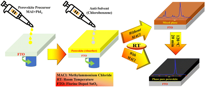 | ||
| Fig. 1 Schematic representation of room temperature formation of MAPbI3 perovskite thin-films with the addition of MACl under ambient conditions. | ||
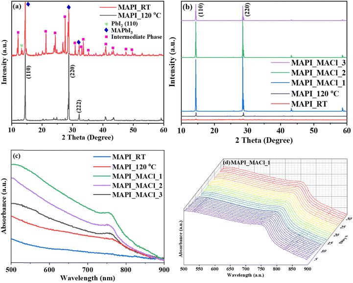
Fig. 2 shows the XRD patterns of all the prepared perovskite samples. The diffraction patterns of MAPI_RT film showed multiple peaks indicating intermediate phases.21 Also, a poor perovskite phase can be observed along with the PbI2 peak (Fig. 2a). In contrast, the MAPI_120 °C film showed a highly crystalline and phase pure perovskite. Fig. 2b demonstrates that all perovskite films exhibit characteristic diffraction peaks at 2θ = 14.0° and 28.4° corresponding to the planes (110) and (220), respectively. Which indicates the complete conversion of the precursor solutions to MAPI perovskite. The peak intensity of MACl added films was observed to be higher than that of pristine MAPI_120 °C. Fig. S1 (in ESI†) shows the intensity comparison of MAPI_120 °C along with the target film MAPI_MACl_1, where it is approximately 14.5 times higher for the later sample. This demonstrates the increased crystallinity and phase purity with the addition of MACl at room temperature under ambient conditions.22 However, the diffraction peak intensity is gradually reducing while increasing the concentration of MACl (Fig. 2b). The excessive amount of MACl in the perovskite film will result in the shrinkage of the perovskite crystals resulting in the reduced diffraction peak intensities.23
UV-visible absorption spectroscopy analysis was performed for all the prepared perovskite thin-films to understand their optical properties and the results are shown in Fig. 2c. It can be observed that the MAPI_RT thin-film shows no absorption in the visible region, but the film annealed at 120 °C shows the absorption edge starting from 790 nm and it absorbs light in the entire visible region. Interestingly, the MACl modified MAPI perovskite thin-films showed strong absorption in the same region and the intensity of the MAPI_MACl_1 film was observed to be higher than that of other perovskite films. There is no peak shift observed with the addition of MACl into the MAPI perovskites. Typically, there will be a peak shift towards the blue region for the mixed halide perovskites. Our results show that there is no peak shift, which may be due to the low content of Cl, indicating that Cl-ions are not replacing the I-ions during perovskite film formation. As we know, MACl is a volatile additive, so it will evaporate easily and regulate the perovskite film morphology and formation energy, which results in the room temperature formation of a phase pure and highly crystalline optically active perovskite phase under ambient conditions.20 Furthermore, we have calculated the optical bandgap of the thin-films by using a Tauc plot. It is observed from Fig. S2 (ESI†) that all the samples showed a band gap of ∼1.53 eV. It has been reported that the organic–inorganic halide perovskites are unstable under ambient, high humidity and high temperature conditions, so it is necessary to examine the stability of the fabricated perovskite thin-films under ambient conditions for a longer period. Hence, UV-Vis absorption measurements for the target sample (MAPI_MACl_1) were studied for over 32 days (Fig. 2d). There is no peak shift or noticeable change in the optical profile observed, which indicates the high optical stability under ambient conditions without any observable degradation.
Another important characteristic of perovskite thin-films is the surface morphology. Fig. 3 shows the surface morphology of the prepared perovskite thin-films. MAPI_120 °C film shows uniform grains with full surface coverage and the size of the grains is around 200–250 nm. The volatile additives MACl generally control the surface morphology resulting in large grain boundaries.20,22 The MAPI_MACl_1 film shows better surface morphology with an increased grain size of about 400 to 500 nm, which is double that of the pristine MAPI_120 °C thin-films. Similarly, the MAPI_MACl_2 film also shows better film morphology with the grain size around 300–400 nm. But in the case of MAPI_MACl_3 the grain size is reduced to ∼300 to 350 nm, which is due to the excess amount of MACl leading to shrinkage in the perovskite crystal formation resulting in a reduced grain size.23 Elemental analysis was conducted by EDAX spectroscopy to understand the elemental composition of the prepared perovskite sample (MAPI_MACl_1) and the result is presented in Fig. S3 (ESI†). All the elements are present in their stoichiometric ratio and there is no chlorine content observed in the sample,22 which agreed with the UV-Vis data.
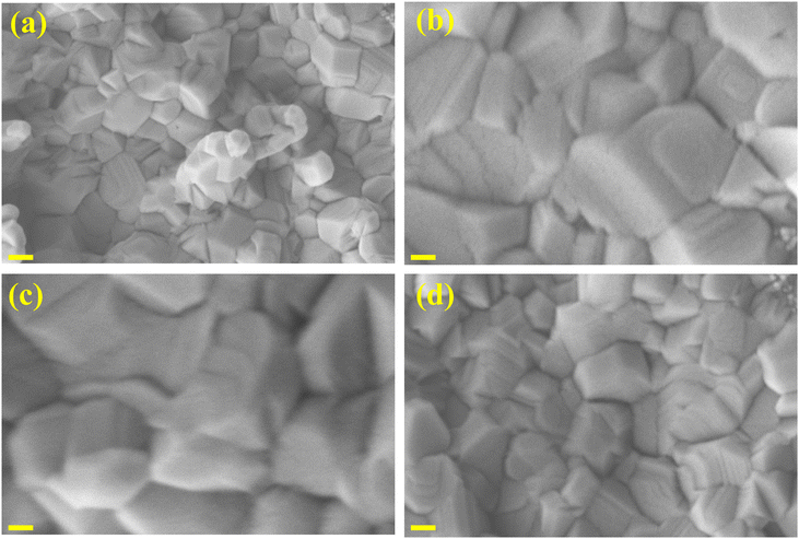 | ||
| Fig. 3 Scanning electron microscope images of the prepared perovskite thin-films (a) MAPI_120 °C, (b) MAPI_MACl_1, (c) MAPI_MACl_2 and (d) MAPI_MACl_3 (scale bar is 200 nm for all the images). | ||
XPS analysis was performed to understand the chemical composition and oxidation states of the perovskite films and Fig. 4 shows the spectra of sample MAPI_MACl_1. The survey spectrum is shown in Fig. 4a, and it can be observed that all the elements are present and there is no chlorine peak present in the sample, which is further evidence for the UV-Vis spectra (no change in the bandgap even after adding MACl into the perovskite solution).20Fig. 4b shows the high-resolution spectrum of C 1s that can be de-convoluted into 3 peaks starting from 284.8 eV, 286 eV and 288.2 eV. In particular, the peaks at 284.8 eV and 286 eV attributed to the sp2 carbon (C–C) from the surface adsorbed species and carbon bonded with nitrogen (C–C) from the surface adsorbed species and carbon bonded with nitrogen (C–N) in the perovskite organic core respectively. The peak at 288.2 eV assigned to the carbon singly bonded with oxygen (C–O), which is also attributed to surface contamination.24,25 High-resolution XPS spectra of I 3d are shown in Fig. 4c, and it can be observed that there are strong peaks at 618.8 eV and 630.3 eV attributed to the 3d5/2 and 3d3/2 respectively. These peaks signify the presence of iodine in the 3− (I3−) oxidation state in the MAPI perovskite films. Fig. 4d shows the high-resolution spectrum of Pb 4f, where the peaks at 138.4 eV and 143.6 eV are attributed to the 4f7/2 and 4f5/2, respectively, which are signature peaks of the 2+ oxidation state of Pb (Pb2+).26 Finally, Fig. 4e shows the high-resolution spectrum of N 1s and shows a high intense peak at low binding energy and the shoulder peak shifted to higher binding energies. The peak at 400 eV is associated with nitrogen singly bonded to carbon (–N–H) and the peak at 402 eV corresponds to the N–H3 singly bonded to the carbon in the MAPI perovskite phase, with these results well matching with the reported literature.24–26
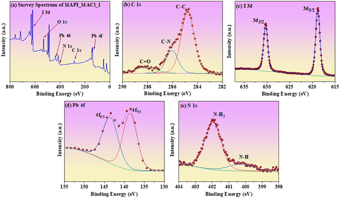 | ||
| Fig. 4 (a) XPS survey spectrum of MAPI_MACl_1 and (b)–(e) high-resolution spectra of C 1s, I 3d, N 1s and Pb 4f, respectively. | ||
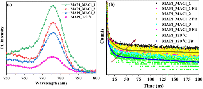
Photoexcited carrier behaviour was investigated using steady-state photoluminescence (PL) spectroscopy and the results are shown in Fig. 5a. It can be observed that all the perovskite thin-films showed prominent PL emission in the 776 nm wavelength region and these results are in good agreement with the UV absorbance data. The peak intensity of MAPI_MACl_1 is found to the very high and is four times higher than that of MAPI_120 °C, indicating the high crystal quality, in agreement with the XRD results and suppressed non-radiative recombination in the perovskite thin-films.20,22 However, the PL peak intensity is gradually decreasing with the increase of the concentration of MACl. The excess amount of MACl leads to shrinkage in the perovskite crystals resulting in reduced grain size as observed from the SEM analysis. The reduced grain size leads to the creation of surface defects on the thin-films. These surface defects may be responsible for the increase in the non-radiative recombination resulting in the reduced PL peak intensity while increasing the concentration of MACl in the MAPI perovskite samples.23 These results were further supported by the time-resolved photoluminescence (TRPL) decay measurements and are shown in Fig. 5b. These curves are fitted with the biexponential function (eqn (1)) containing both τ1 and τ2, indicating fast and slow decay lifetimes, respectively, where τ1 and τ2 are the PL decay times and A1 and A2 are the amplitudes.23,27 The fast decay component τ1 indicates charge carrier quenching at the interface and nonradiative recombination caused by charge trapping defects and the slow decay component τ2 represents the bulk recombination of charge carriers.28 Table S1 (ESI†) shows the charge carrier lifetime of all the perovskite thin-films. The τ1 value of MAPI_MACl_1 was calculated to be 9.6 ns, which is higher than that of MAPI_ 120 °C (5.4 ns) indicating that MAPI_MACl_1 has minor surface defects resulting in the reduced nonradiative recombination, which is confirmed by surface morphology observed from the SEM analysis. The higher τ2 value of MAPI_MACl_1 indicates that the recombination in the bulk perovskite thin-film is also efficiently reduced.23
 | (1) |
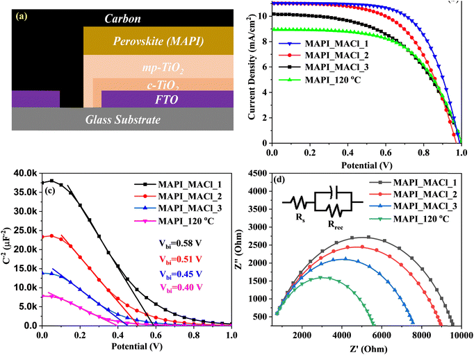
The photovoltaic performance of MACl-modified MAPI perovskite solar cells was fabricated with a carbon-based HTL-free device architecture (Fig. 6a) under ambient conditions with relative humidity around (50–60%) at room temperature. The solar cell J–V results are shown in Fig. 6b. The power conversion efficiency of our champion device (MAPI_MACl_1) is 7.11% with Voc of 0.98 V and the Isc is 11.03 mA cm−2 which is much higher than that of pristine MAPI_120 °C of 5.27% (Voc: 1.0 V and Isc: 8.95). All the solar cell parameters are summarized in Table 1. The FF of our champion device MAPI_MACl_1 of ∼65.86% is higher as compared with all the other devices due to the better charge transport at the interfaces.
| Sample | V oc | I sc | FF | PCE |
|---|---|---|---|---|
| MAPI_120 °C (RS) | 1.01 | 8.95 | 58.82 | 5.27 |
| MAPI_120 °C (FS) | 1.00 | 8.98 | 52.31 | 4.70 |
| MAPI_MACl_1 (RS) | 0.98 | 11.03 | 65.86 | 7.11 |
| MAPI_MACl_1 (FS) | 0.98 | 11.06 | 57.02 | 6.18 |
| MAPI_MACl_2 (RS) | 0.96 | 11.02 | 59.29 | 6.27 |
| MAPI_MACl_2 (FS) | 0.96 | 11.05 | 53.61 | 5.69 |
| MAPI_MACl_3 (RS) | 1.00 | 10.17 | 52.22 | 5.31 |
| MAPI_MACl_3 (FS) | 1.00 | 10.27 | 46.41 | 4.77 |
All the devices showed a hysteresis effect, which is due to the weak interaction between the two layers in the perovskites solar cell resulting in defect generation (Fig. S4, ESI†). These defects are responsible for the increase in the hysteresis in the perovskite solar cells. There are different ways to reduce the hysteresis in the perovskite solar cells, such as improving the charge transporting ability via optimizing the charge transport layers, stabilizing perovskite materials and finding more suitable materials and finally, reducing the traps via optimizing the interfaces between the perovskite and charge transport layers.29 In addition, we have done a stability study of the fabricated perovskite solar cells (Fig. 7). The device showed high stability over the period of 10 days stored under ambient conditions while retaining 80% of its initial efficiency. Whereas the pristine device showed a PCE of 5.27% and decreased ∼50% of its initial efficiency within 5 days. The enhanced photovoltaic performance of MAPI_MACl_1 is due to the reduced recombination of photogenerated charge carriers. The recombination behaviour of charge carriers was further investigated by using electrochemical impedance spectroscopy (EIS). The EIS measurements were done for all the fabricated devices and the results are shown in Fig. 6d. The MAPI_MACl_1 device shows high recombination resistance as compared to the other devices, which is attributed to the clean interface between the perovskite and other charge transport layers which is due to the incorporation of MACl.30 Furthermore, to understand the interface contact between the perovskite/ETL and perovskite/carbon we conducted Mott–Schottky measurements for the fabricated devices. The built-in potential (Vbi) was obtained by fitting the linear region of the plot, as shown in Fig. 6c. It was observed that the device MAPI_MACl_1 shows a higher Vbi (0.58 V) as compared with the rest of the devices. This indicates that the larger Vbi not only suppresses the reverse transport of photogenerated charge carriers at the interface but also enhances the charge separation. That corroborates with the results obtained in impedance spectroscopy.31 Typically, to attain high power conversion efficiency in the solar cell, the series resistance (Rs) should be low and the shunt resistance (Rsh) should be high. If the Rs is high, electrons cannot move freely along the circuit, and if the Rsh is low, leakage current will occur, which results in poor performance for the solar cell device. Fig. S5(a and b) (ESI†) shows the shunt and series resistance for all the perovskite solar cells and the values are summarized in Table S2 (ESI†). Fig. S5c (ESI†) shows the equivalent circuit diagram of the perovskite solar cell device. Interestingly, it is observed form Fig. S5(a and b) (ESI†) that the values for Rsh are higher (∼5882 Ω), whereas Rs (∼20.80 Ω) is lower for the MAPI_MACl_1 device indicating the better charge transport at both the interfaces between the perovskite and carbon and the perovskite and ETL. EIS analysis also corroborates with the above studies that when the recombination resistance was observed to be higher it facilitates the lower charge recombination at the interface resulting in a high power conversion efficiency.32 As previously discussed, MACl regulates the surface morphology of the perovskite thin-films by increasing the grain size in the order of 2, and MACl induces the room temperature formation of phase pure perovskite thin-films resulting in the high photovoltaic performance of the MACl-modified MAPI perovskite thin-films under ambient conditions.
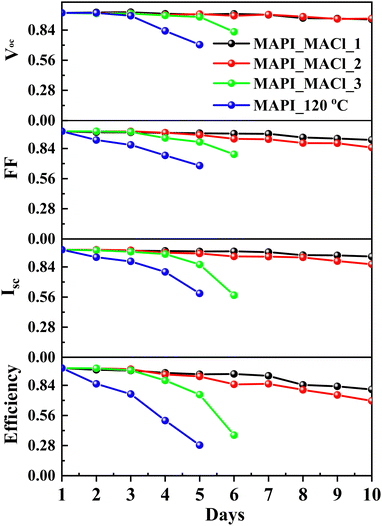 | ||
| Fig. 7 Stability of the fabricated perovskite solar cells stored under ambient conditions over 10 days (normalized Voc, FF, Isc and PCE). | ||
Conclusions
In conclusion, we have demonstrated the HTL-free carbon-based perovskite solar cell device architecture fabricated under ambient conditions at room temperature. The MACl-modified perovskite solar cell devices showed enhanced power conversion efficiency of 7.11% with high stability over a period of 10 days stored under ambient atmosphere and retained 80% of their initial efficiency. This enhanced performance is due to the incorporation of MACl into the MAPI perovskite material. Which induces the room temperature formation of the phase pure semiconductor grade perovskite confirmed by XRD analysis. MACl modified films showed improved surface morphology with increased grain size on the order of 2 times as compared with the pristine one, which was confirmed by the SEM results. The enhanced optoelectronic properties of the MACl-modified films were studied by using UV-Vis, PL and lifetime analysis. The target films showed the enhanced optoelectronic properties, such as high absorption in the visible region, and showed enhanced PL emission, which indicated reduction in the non-radiative recombination. Furthermore, these results were supported by electrochemical impedance spectroscopy, which confirms the increased recombination resistance for the MACl added perovskite solar cells. This indicates improved charge carrier mobility in the device resulting in the high power conversion efficiency. This device architecture may be further used to fabricate stable ambient processed perovskite solar cells on a large scale to make them commercially viable.Author contributions
Pardhasaradhi Nandigana: conceptualization, methodology, data generation, data curation and writing original draft. Bhavadarini S: synthesis of materials and characterization. Sriram P: original draft correction. Sujatha D: carbon paste preparation. Imthiaz and Ram Prasanth R: literature survey and characterization and plotting. Subhendu K. Panda: supervision, investigation, editing final draft.Conflicts of interest
There are no conflicts to declare.Acknowledgements
The authors are thankful for the funding support from the CSIR FTT project (MLP-0407). Pardhasaradhi N. is grateful for the fellowship from UGC-SRF (191620061516). Thanks go to Central instrumentation facility of CSIR-Central Electrochemical Research Institute, Karaikudi for sample characterization. CSIR-CECRI manuscript communication number: CECRI/PESVC/Pubs/2023-120.References
- D. Weber, Z. Naturforsch., B: J. Chem. Sci., 1978, 33, 1443–1445 CrossRef.
- C. Wehrenfennig, G. E. Eperon, M. B. Johnston, H. J. Snaith and L. M. Herz, Adv. Mater., 2014, 26, 1584–1589 CrossRef CAS PubMed.
- Y. Zhao and K. Zhu, Chem. Soc. Rev., 2016, 45, 655–689 RSC.
- T. Jesper Jacobsson, J. P. Correa-Baena, M. Pazoki, M. Saliba, K. Schenk, M. Grätzel and A. Hagfeldt, Energy Environ. Sci., 2016, 9, 1706–1724 RSC.
- A. Kojima, K. Teshima, Y. Shirai and T. Miyasaka, J. Am. Chem. Soc., 2009, 131, 6050–6051 CrossRef CAS.
- H. S. Kim, C. R. Lee, J. H. Im, K. B. Lee, T. Moehl, A. Marchioro, S. J. Moon, R. Humphry-Baker, J. H. Yum, J. E. Moser, M. Grätzel and N. G. Park, Sci. Rep., 2012, 2, 1–7 Search PubMed.
- https://www.nrel.gov/pv/cell-efficiency.html .
- W. J. Yin, Y. Yan and S. H. Wei, J. Phys. Chem. Lett., 2014, 5, 3625–3631 CrossRef CAS.
- D. Liu, C. Yang, M. Bates and R. R. Lunt, iScience, 2018, 6, 272–279 CrossRef CAS PubMed.
- M. Bari, H. Wu, A. A. Bokov, R. F. Ali, H. N. Tailor, B. D. Gates and Z. G. Ye, CrystEngComm, 2021, 23, 3326–3339 RSC.
- L. Zhang, C. Zuo and L. Ding, J. Semicond., 2021, 42, 72201 CrossRef CAS.
- Z. Yang, J. Pan, Y. Liang, Q. Li and D. Xu, Small, 2018, 14, 1802240 CrossRef PubMed.
- M. Liu, Z. Chen, Q. Xue, S. H. Cheung, S. K. So, H. L. Yip and Y. Cao, J. Mater. Chem. A, 2018, 6, 16347–16354 RSC.
- B. Yang, C. C. Brown, J. Huang, L. Collins, X. Sang, R. R. Unocic, S. Jesse, S. V. Kalinin, A. Belianinov, J. Jakowski, D. B. Geohegan, B. G. Sumpter, K. Xiao and O. S. Ovchinnikova, Adv. Funct. Mater., 2017, 27, 1700749 CrossRef.
- Y. Zhao and K. Zhu, J. Phys. Chem. C, 2014, 118, 9412–9418 CrossRef CAS.
- F. Xu, T. Zhang, G. Li and Y. Zhao, ChemSusChem, 2017, 10, 2365–2369 CrossRef CAS.
- H. Tsai, W. Nie, P. Cheruku, N. H. MacK, P. Xu, G. Gupta, A. D. Mohite and H. L. Wang, Chem. Mater., 2015, 27, 5570–5576 CrossRef CAS.
- P. Docampo, F. C. Hanusch, S. D. Stranks, M. Döblinger, J. M. Feckl, M. Ehrensperger, N. K. Minar, M. B. Johnston, H. J. Snaith and T. Bein, Adv. Energy Mater., 2014, 4, 1–6 Search PubMed.
- Q. Chen, H. Zhou, Y. Fang, A. Z. Stieg, T. Bin Song, H. H. Wang, X. Xu, Y. Liu, S. Lu, J. You, P. Sun, J. McKay, M. S. Goorsky and Y. Yang, Nat. Commun., 2015, 6, 1–9 CAS.
- M. Kim, G. H. Kim, T. K. Lee, I. W. Choi, H. W. Choi, Y. Jo, Y. J. Yoon, J. W. Kim, J. Lee, D. Huh, H. Lee, S. K. Kwak, J. Y. Kim and D. S. Kim, Joule, 2019, 3, 2179–2192 CrossRef CAS.
- X. Guo, C. McCleese, C. Kolodziej, A. C. S. Samia, Y. Zhao and C. Burda, Dalton Trans., 2016, 45, 3806–3813 RSC.
- L. Bi, Q. Fu, Z. Zeng, Y. Wang, F. R. Lin, Y. Cheng, H. L. Yip, S. W. Tsang and A. K. Y. Jen, J. Am. Chem. Soc., 2023, 145, 5920–5929 CrossRef CAS PubMed.
- D. Liu, C. Li, C. Zhang, Z. Wang, H. Zhang, J. Tian and S. Pang, RSC Adv., 2017, 7, 51944–51949 RSC.
- C. Rocks, V. Svrcek, T. Velusamy, M. Macias-Montero, P. Maguire and D. Mariotti, Nano Energy, 2018, 50, 245–255 CrossRef CAS.
- C. Rocks, V. Svrcek, P. Maguire and D. Mariotti, J. Mater. Chem. C, 2017, 5, 902–916 RSC.
- G. Rajendra Kumar, A. Dennyson Savariraj, S. N. Karthick, S. Selvam, B. Balamuralitharan, H. J. Kim, K. K. Viswanathan, M. Vijaykumar and K. Prabakar, Phys. Chem. Chem. Phys., 2016, 18, 7284–7292 RSC.
- S. Pari, P. Nandigana and S. K. Panda, ACS Appl. Opt. Mater., 2023, 1, 802–809 CrossRef CAS.
- E. Khorshidi, B. Rezaei, D. Blätte, A. Buyruk, M. A. Reus, J. Hanisch, B. Böller, P. Müller-Buschbaum and T. Ameri, Sol. RRL, 2022, 6, 2200023 CrossRef CAS.
- P. Liu, W. Wang, S. Liu, H. Yang and Z. Shao, Adv. Energy Mater., 2019, 9, 1803017 CrossRef.
- Y. Yang, K. Ri, A. Mei, L. Liu, M. Hu, T. Liu, X. Li and H. Han, J. Mater. Chem. A, 2015, 3, 9103–9107 RSC.
- Q. Xiong, L. Yang, Q. Zhou, T. Wu, C.-L. Mai, Z. Wang, S. Wu, X. Li and P. Gao, ACS Appl. Mater. Interfaces, 2020, 12, 46306–46316 CrossRef CAS.
- D. I. Kim, J. W. Lee, R. H. Jeong and J.-H. Boo, Sci. Rep., 2022, 12, 697 CrossRef CAS.
Footnote |
| † Electronic supplementary information (ESI) available. See DOI: https://doi.org/10.1039/d3ya00500c |
| This journal is © The Royal Society of Chemistry 2024 |

