
Deformation behavior and yield strength prediction of [112] oriented NbMoTaW refractory high entropy alloy nanowires†
Taozhi
Tian
a,
Tao
Fu
 *ac,
Mengye
Duan
a,
Hao
Hu
a,
Chuanying
Li
a,
Xiang
Chen
*b and
Xianghe
Peng
*a
*ac,
Mengye
Duan
a,
Hao
Hu
a,
Chuanying
Li
a,
Xiang
Chen
*b and
Xianghe
Peng
*a
aDepartment of Engineering Mechanics, Chongqing University, Chongqing 400044, China. E-mail: futao@cqu.edu.cn; xhpeng@cqu.edu.cn
bInstitute for Advanced Sciences, Chongqing University of Posts and Telecommunications, Chongqing, 400065, China. E-mail: chenxiang@cqupt.edu.cn
cState Key Laboratory of Coal Mining Disaster Dynamics and Control, Chongqing University, Chongqing, 400044, China
First published on 16th December 2024
Abstract
Refractory high entropy alloys (RHEAs) have garnered widespread attention due to their potential applications at extremely high temperatures. However, accurately predicting the mechanical properties of these materials is challenging due to the complex slip systems in body-centered cubic (BCC) metals. In this work, the tensile behaviors of NbMoTaW RHEA single crystalline nanowires with various radii under tensile deformation were investigated using molecular dynamics simulations, focusing on their deformation behavior, mechanical response, and size-dependent effects. The results revealed a transition in yield stress from the Hall–Petch relation to the inverse Hall–Petch relation with the decrease of the nanowire radius. The primary deformation mechanism observed was the nucleation and glide of dislocation from the surface. A thermal activation-based theoretical model was developed for determining the yield stress, incorporating stacking fault energy and surface energy as pivotal parameters. This model could effectively predict the yield stress of the RHEA in the inverse Hall–Petch stage and exhibit significant potential in predicting the mechanical properties of other BCC metals.
1. Introduction
BCC refractory high entropy alloys (RHEAs), such as NbMoTaW and NbMoTaWV,1 have attracted considerable attention due to their exceptional properties, including high strength, thermal stability, and resistance to high temperatures and oxidation.2–5 These properties make them promising candidates for applications in aerospace, biomedicine, and the development of radiation-resistant materials. Extensive research has demonstrated the importance of microstructure and characteristic dimensions of nanomaterials in determining their mechanical properties, particularly strength and toughness. Consequently, there is considerable interest in the design and optimization of these mechanical properties by tailoring their microstructure and size in the fields of materials science and engineering.6–8Nanowires (NWs), as a kind of one-dimensional material with diameters typically below 100 nm, exhibit remarkable mechanical, electromagnetic, and optical performance, making them highly versatile for applications in wearable devices,9,10 nanogenerators,11 water purification,12 biosensors13,14 and other fields. The small size of nanowires makes their mechanical properties particularly sensitive to their radius, leading to the size effects similar to those observed in polycrystalline materials. While the Hall–Petch (HP) relation15,16 generally shows a ‘smaller is stronger’ correlation between grain size and yield strength in most metals,15 this trend may shift to the inverse Hall–Petch (IHP) relation when the grain size is reduced to a few nanometers,17,18 characterized by “the smaller, the weaker”.19,20 This shift can be attributed to a change in the deformation mechanism from dislocation-dominated activity to grain boundary (GB)-dominated behavior, such as GB sliding or migration21–24 and grain rotation.25,26 For single-crystalline materials like nanowires, numerous studies have shown the strong size-dependence of their mechanical properties,27–29 like HP. However, as the sample size is further decreased, the HP relation may transition to the IHP relation; analogous to the role of GBs in polycrystalline materials, the surface effect30–32 may become a crucial factor affecting the mechanical properties of NWs due to the sharp increase in surface content.
Although extensive research has been conducted on FCC metals, investigations on BCC metals are still in the nascent stages, primarily due to the complexity and uncertainty of their deformation behaviors. Unlike the stable slip system in FCC metals, the deformation behavior of BCC metals is highly dependent on the loading direction,33–35 and exhibits remarkable tension-compression asymmetry.36–38 Slip in BCC metals can occur on multiple slip planes (such as {110}, {112}, {123}), even with a consistent slip direction along the 〈111〉 direction, leading to a competition between dislocation glide and twinning.39,40 While some studies have elucidated the deformation behavior and predominant mechanisms of BCC nanowires under loading along specific orientations,34,41 a unified theory that can comprehensively describe this phenomenon is still lacking. Consequently, predicting the mechanical properties of BCC metals remains a significant challenge.
Conventional models for predicting mechanical properties usually rely on empirical formulas, which may encounter challenges when applied to materials with smaller dimensions. To address these challenges, various alternative models have been proposed from diverse viewpoints, aiming to offer more effective descriptions and predictions of mechanical properties. For instance, one innovative approach differs from the traditional crystal plasticity by assigning a slip system to each Burgers vector, which facilitates the replication of the results obtained by molecular dynamics (MD) simulations and provides valuable insights into the plasticity of single crystals.42 Zhao et al. proposed a model that addresses the size-dependent fracture mechanisms of nanowires by identifying critical aspect ratios that describe the relation between the fracture strain and aspect ratio.27 Additionally, machine learning techniques have been utilized to determine the influencing factors of fitting parameters (σ0 and k) in the HP relation, enabling the development of new relations based on key parameters without relying on constant experimental data fitting.43 In material–property-based models for nanopolycrystalline metals, the GBs are treated as distinct phases from the grain interior, allowing for the assessment of the maximum strength based on the activation energy required for the transition between crystalline and amorphous phases.44 Notably, the amorphous model44 not only effectively predicted the mechanical properties of BCC Ta at the IHP stage but also showed great potential for predicting mechanical properties of other materials.45,46
In this work, the mechanical responses of the NbMoTaW nanowires with different radii under tension are studied using MD simulations, to explore the deformation mechanisms and the key factors affecting the mechanical properties of these nanowires at the IHP stage. Additionally, a theoretical model is developed for predicting the yield stress. In section 2, the establishment of nanowire samples and MD simulation details are introduced. In section 3, the mechanical responses and deformation mechanism of the NbMoTaW nanowires with different radii under tension are presented and discussed. In section 4, a theoretical model incorporating thermal activation is developed, which is used to describe the yield stress of nanowires and is extended to predict the mechanical properties of other BCC metals. Finally, conclusions are drawn in section 5.
2. Simulation details
In this work, the spectral neighbor analysis potential (SNAP) parameters identified by Li et al.47 are utilized to describe the interatomic interaction in NbMoTaW RHEAs. The single-crystalline nanowires with orientations of x//[1![[1 with combining macron]](https://www.rsc.org/images/entities/char_0031_0304.gif) 1], y//[10], and z//[112] are built using the software ATOMSK.48 These nanowires have radii R ranging from 2 nm to 15 nm and a fixed height of 8 nm, with an atomic composition of Nb
1], y//[10], and z//[112] are built using the software ATOMSK.48 These nanowires have radii R ranging from 2 nm to 15 nm and a fixed height of 8 nm, with an atomic composition of Nb![[thin space (1/6-em)]](https://www.rsc.org/images/entities/char_2009.gif) :Mo:Ta:W set as 1:1:1:1 (equal atomic ratio), as shown in Fig. 1.
:Mo:Ta:W set as 1:1:1:1 (equal atomic ratio), as shown in Fig. 1.
 | ||
| Fig. 1 Atomic configuration and cross-section of the NbMoTaW RHEA nanowire with a radius (R) of 4 nm and the loading direction of [112]. (a) Cross-section with atoms colored by the element type. (b) Cross-section with atoms colored by the local structure, with blue and white balls denoting inner and surface layer atoms, respectively. | ||
All MD simulations are conducted using LAMMPS.49 Periodic boundary conditions are applied in the x, y, and z directions, with a vacuum layer in the radial direction to mimic the surface of nanowires. Prior to the mechanical test, the samples undergo a 30 ps relaxation at 10 K under NPT ensemble, maintaining zero pressure in all directions to achieve a stable system. Subsequently, the nanowires are uniaxially stretched at a strain rate of 1 × 10⁹ s−1 in the z direction at 10 K using NVT ensemble, with the maximum strain of 0.2. The timestep is set to 1 fs. Since the calculated tensile stress corresponds to the stress of the simulation box along the z axis, it is necessary to convert it to the tensile stress of the nanowire due to the introduction of a vacuum layer in the radial direction. This is done using the relation σNW = σBox × SBox/SNW, where σNW is the tensile stress of the nanowire, σBox is the z-axis tensile stress of the box, SBox is the cross-sectional area of the simulation box in the z direction, and SNW = πR2 is the cross-section area of the nanowire, with R as the nanowire radius.
To account for latent effects of atomic distribution in the RHEAs, three sets of samples (labeled as sample groups A, B, and C) with different random seeds are built to enhance the statistical robustness and reliability of our results. All the simulations are performed under identical loading conditions. Microstructure analysis and visualization are carried out using OVITO,50 where blue balls represent the internal atoms in the BCC lattice, white balls denote surface atoms or defects, and green and pink lines indicate the 〈111〉 and 〈110〉 type dislocations.
3. Results and discussion
Fig. 2(a)–(c) show the stress–strain (σ–ε) curves of sample groups A, B, and C, respectively. These curves exhibit similar trends, initially showing nearly linear growth until reaching the yield stress, with slight variations in slope. At a strain of approximately 0.13 (ε ≈ 0.13), all the samples begin to yield, characterized by a rapid drop in stress from the peak (yield stress), followed by a plastic flow stage where stress fluctuates within a certain range as strain increases. Fig. 2(d) shows the variation of yield stress with the radius R, revealing a trend analogous to the HP and IHP relations, with a critical transition radius around 6 nm. In the range of R > 6 nm, the yield stress increases with the decrease of R, consistent with the HP stage and showing a “the smaller, the stronger” trend. Conversely, for R < 6 nm, the yield stress decreases with the decrease of R, aligning with the IHP stage and reflecting a trend of “the smaller, the weaker”. Notably, the stress change in the IHP stage is within 2 GPa, which differs from the IHP stages observed in Mo (ref. 35) and Fe (ref. 51) nanowires, where stress changes exceed 3 GPa. This discrepancy can be attributed to that the radius R we used corresponds to the minimum sample diameter of d = 4 nm, which is larger than the diameter of d = 1 nm for BCC Mo (ref. 35) and d = 1.42 nm for BCC Fe.51 Additionally, it can be seen that the yield stress would not saturate with the increase of radius but transitions into the HP stage. A similar transition has also been observed in 〈111〉 oriented Mo nanowires,35 supporting our results. | ||
| Fig. 2 (a)–(c) Stress–strain curves of sample groups A, B, and C with different R. (d) Variation of yield stress with R, revealing a transition from the HP relation to the IHP relation at R = 6 nm. Simulations on sample group A with R = 2 nm at different strain rates confirm that the deviation of the yield stress obtained with different strain rates remains within the error range. | ||
In order to assess the effect of the strain rate, additional simulations on sample group A with R = 2 nm are conducted at various strain rates. The results [Fig. 2(d)] show that the yield stress at a strain rate of 1 × 10⁹ s−1 differs only slightly from those at lower strain rates (1 × 10⁸ s−1 to 5 × 10⁸ s−1), with all values falling within the error range, which confirms that the strain rate of 1 × 10⁹ s−1 is reasonable for this study. Furthermore, although the SNAP potential used in this work is highly accurate, it has relatively low computational efficiency. Therefore, we selected 1 × 10⁹ s−1 as the strain rate to balance the requirement of accuracy and computational efficiency.
Fig. 3(a) shows the σ–ε curve of the nanowire with R = 4 nm, where yield occurs at ε ≈ 0.13. To analyze the microstructure evolution and dominant deformation mechanism, the microstructures corresponding to the feature points (points b to f) in the σ–ε curve are presented in Fig. 3(b)–(f), respectively. At ε = 0.135, a dislocation nucleates from the surface, where the local energy is relatively high [Fig. 3(b)]. As ε increases to 0.137, the dislocation grows and glides along the slip plane [Fig. 3(c)]. Simultaneously, a second dislocation nucleates from the surface on the other side [Fig. 3(c)], leading to the interconnection and intertwining of multiple dislocations within the nanowires as ε reaches 0.139 [Fig. 3(d)]. At this stage, twin nucleation begins, accompanied by a significant drop in stress [from points b to d in Fig. 3(a)]. As ε further increases to 0.15, the dislocation count decreases, and the stress falls to the bottom of the valley [point e in Fig. 3(a)]; the twin becomes more distinct [Fig. 3(e)]. At ε = 0.20, dislocations nearly disappear, the edges of twin boundaries (TBs) gradually migrate towards the surface, and numerous scattered defects appear within the nanowires [Fig. 3(f)]. Slicing the nanowires and observing the TBs along the 〈111〉 direction reveals that the TBs noticeably shorten from ε = 0.15 to ε = 0.2, with their positions migrating from the center towards the periphery of the nanowires [Fig. 3(g) and (h)]. Substantial deformation is observed, with the {110} plane identified as the slip plane, forming a slip band comprising five atomic layers [Fig. 3(i)]. This deformation mode aligns well with the experimental result of W nanowires subjected to tension in the same direction.52
 | ||
| Fig. 3 (a) Stress–strain curve of a nanowire sample with R = 4 nm, with points b–f as feature points. (b)–(f) Top views of microstructures of the nanowire sample at points b–f in (a), illustrating the dislocation nucleation process. Atoms in the perfect BCC lattice have been removed for clarity, with white atoms indicating the surface or defect sites, green lines representing 〈111〉 dislocations, and pink lines representing 〈110〉 dislocations. (g) and (h) Slices of nanowires revealing twin boundaries at ε = 0.15 and ε = 0.2, respectively. (i) Formation of the slip band observed at ε = 0.2. | ||
The Young's modulus E is defined as the slope of the stress–strain (σ–ε) curve prior to dislocation nucleation. In our work, the Young's moduli of the nanowires with different radii are calculated with the σ–ε curves in the strain range from 0 to 0.05. It can be seen in Fig. 4 that E decreases gradually with the decrease of the nanowire radius. The E of the nanowires with different radii can be described using the rule of mixture (ROM):53
| E = f0E0 + f1E1 | (1) |
 | ||
| Fig. 4 Comparison of Young's moduli (E) of nanowires with varying R from eqn (1) and MD results. | ||
The microstructure evolutions of the nanowires with other R under tension are also analyzed. Due to the absence of internal defects, the surface atoms of the nanowires have higher energy compared with the internal atoms, leading to dislocation nucleation initiating from the surface. Throughout the simulation, twin nucleation consistently follows the nucleation of dislocations, indicating that the deformation mechanism is mainly dislocation-dominated. This is because twinning typically involves the {112}〈111〉 slip system, while in BCC metals, slip systems are temperature-dependent, and at low temperatures, the {110} plane is often preferred.54 In this work, tension tests on nanowires are conducted at a low temperature of 10 K, favoring the {110}〈111〉 slip system, thus facilitating the generation of dislocations. Slip occurs when the resolved shear stress on a slip system exceeds a critical value. The Schmid factor can describe the relation between the applied tensile stress and the resolved shear stress, and the Schmid factor for the two slip systems can be calculated: the {110}〈111〉 slip system corresponding to dislocation nucleation has a Schmid factor of μ1 = 0.41, and the {112}〈111〉 slip system corresponding to twining has a Schmid factor of μ2 = 0.39.55 Since μ1 > μ2, dislocation nucleation should be the dominant deformation mechanism. As R increases, the number of dislocations nucleating from the surface increases, along with the capacity to store dislocations. The number of dislocations increases rapidly after yield, and subsequently decreases with the increase of strain. As ε = 0.2, dislocations in the nanowire samples with smaller radii tend to annihilate, while some dislocations may persist in the samples with larger radii.
4. Model construction and validation
As discussed in section 3, the primary deformation mechanism for the yield of the NbMoTaW nanowires is the nucleation of dislocation from the surface, followed by dislocation slip and the formation of the slip band as strain increases. The grain size effect, characterized by the fact that the smaller the grain size, the higher the grain boundary fraction, would significantly affect the mechanical properties of polycrystalline materials. Similarly, in nanowires, a reduction in the sample radius would also result in a higher proportion of the surface area. The surface, which would increase the energy of a system due to the introduction of additional surface energy, would lower the energy barrier for dislocation nucleation, accounting for the observed IHP-like relation. Therefore, the surface proportion should be considered as a crucial factor in evaluating the influence of the surface on the mechanical properties of nanowires.The local microstructure of the samples is examined using DXA56 in OVITO, revealing that the surface proportion of the nanowires increases from approximately 5% at R = 15 nm to around 25% at R = 2 nm. To determine the surface proportion, the outermost atoms of the nanowires are defined as the surface layer atoms, with a layer of atoms perpendicular to the axis being intercepted. The interatomic distance ranges from 0.707a to 0.866a (a is the lattice constant), and a thickness of 0.866a is selected for the outermost surface layer thickness. This method enables the calculation of the surface proportion of nanowires in the cross-section for different radii and lattice constants (more details are available in section S1 in the ESI†). The results obtained are consistent with those by DXA in OVITO, supporting the selection methodologies outlined in the relevant literature.57
Chandross et al.44 proposed a theoretical model to predict the strength of materials through thermal activation theory, which is based on the energy barrier associated with the transition between crystalline and amorphous phases. The model can be expressed as:
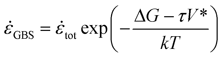 | (2) |
![[small epsi, Greek, dot above]](https://www.rsc.org/images/entities/i_char_e0a1.gif) GBS is the strain rate related to GB sliding, which can be viewed as the strain rate related to GB behavior here; tot is the total (applied) strain rate; ΔG is the activation energy; τ is the shear stress; V* is the activation volume; k is the Boltzmann constant and T is the temperature. By applying the Taylor expansion to eqn (2), one obtains:
GBS is the strain rate related to GB sliding, which can be viewed as the strain rate related to GB behavior here; tot is the total (applied) strain rate; ΔG is the activation energy; τ is the shear stress; V* is the activation volume; k is the Boltzmann constant and T is the temperature. By applying the Taylor expansion to eqn (2), one obtains: | (3) |
In MD simulations, it is usually assumed that the two strain rates (GBS and tot) are approximately equal,44 and thus, eqn (3) can be simplified to:
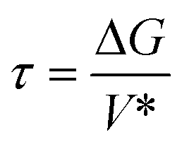 | (4) |
To predict the strength of nanotwinned metals, Xiao et al.45 considered their yield as the result of combined contributions of grain boundary melting and phase transition, and introduced an innovative energy activation model to quantify the energy required for phase transitions. Drawing inspiration from their work, in this work, we also treat the nucleation of dislocation and the formation of a stacking fault from the surface of nanowires as a phase transition. During the yield of the nanowires, dislocation activation and glide lead to the formation of a stacking fault, while new surfaces are formed. Therefore, the activation energy of these behaviors can be expressed in terms of the stacking fault energy (γSFE) and surface energy (γSUR) as:
| ΔG = ΔG(γSFE,γSUR) | (5) |
We then calculate the required γSFE and γSUR. The calculation of γSFE involves the construction of a bulk sample and the determination of the maximum energy needed for sliding along the 〈111〉 direction on the {110} plane (further details can be found in section S2 of the ESI†). On the other hand, γSUR is directly calculated by using the established nanowire sample (more details are provided in section S3 of the ESI†). As a result, the values of γSFE and γSUR of the nanowires are determined to be 1.363 J m−2 and 2.615 J m−2, respectively. Notably, compared with γSFE, the higher γSUR supports our hypothesis that the surfaces of the nanowires with smaller radii may exert a more significant influence on their yield stress.
The activation process of dislocation is illustrated in Fig. 5(a). To facilitate the construction of the model, we set the height of the model to be perpendicular to the {110} plane. First, we assume that the area of dislocation nucleation is much smaller than the surface of the nanowire sample. Therefore, at the site where dislocation nucleates, we simplify the curved surface as a plane. The orange plane represents the simplified surface, and plane A is concaved into the nanowire under the influence of the dislocation nucleation, which form the curved surface B, and the top and bottom of surface B are semicircles C with radius r. The contribution of γSFE and γSUR to the activation energy corresponds to the change of their relevant area in the activation model. The area corresponding to the contribution of γSFE is S1= (π − 2)rh, which is the increased area from plane A to curved surface B, and the area corresponding to the contribution of γSUR is S2= πr2/2, which is the area of the new surface C. Here, r is the distance at which the stacking fault occurs and is set to 0.433a, and h is the atomic distance in the 〈110〉 direction and is set to 0.707a. Smoluchowski et al.58 suggested that the presence of a surface on nanowires could lower the energy barrier for dislocation nucleation, making nucleation easier. By using the surface proportion suggested previously as the influence factor for reducing the stacking fault energy barrier, the corresponding contribution of γSFE is weakened, with the degree of weakening being dependent on the radius of nanowires. Hence, the activation energy can be expressed as:
 | (6) |
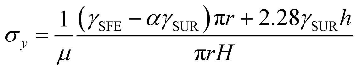 | (7) |
 | ||
| Fig. 5 (a) Schematic of dislocation activation from the surface of the nanowire (orange plane). (b) Comparison of yield stresses of NbMoTaW nanowire samples with different R obtained using theoretical model predictions [red curve, eqn (7) for the IHP stage; blue curve, fitting curve using the HP relation] with that simulated using MD (black points). | ||
Substituting the parameters into eqn (7) and comparing the results with the MD results, as shown in Fig. 5(b), one can see that the predicted curve aligns well with the MD simulation results. With the increase of R, the stress increases initially, then flattens out gradually. The yield stress predicted aligns well with the MD results at the IHP stage, specifically, in the range of 2 nm < R < 6 nm.
To evaluate the predictive capability of the model for the mechanical properties of various BCC metal nanowires, we select the constituent metals of RHEAs and other metals or alloys for verification. To ensure the accuracy of the results for single-component metals and minimize the influence of the difference in sample size,59 samples with a predefined radius and a radius deviation of ±0.1 nm are built (e.g., R = 2 nm represents the average of R = 1.9 nm, 2.0 nm and 2.1 nm). The average value of the three sets of simulations is taken as the yield stress, WTa alloys are treated similarly to RHEAs, and their yield stress, γSFE, and γSUR are obtained under the same simulation conditions. Although the deformation mechanisms of some metals are dominated by twinning rather than dislocation nucleation, it is important to note that both dislocation nucleation and twinning are initiated by partial dislocations.7,60 Therefore, using γSFE as a consistent descriptor for yield stress is justified.
Two types of results are obtained: one exhibits the IHP relation and the other does not;18 here we only choose the former for discussion (other results can be found in section S4 of the ESI†). Several metals show the IHP relation, including W, Mo, Fe, and WTa; a verification range of 2 nm ≤ R ≤ 7 nm is selected for the comparison of the results predicted using eqn (7) with those obtained using MD simulations, as shown in Fig. 6. The yield stress obtained using MD simulations also takes the average of the results of the three samples. The γSUR and γSFE used in eqn (7) for each metal are calculated and shown in section S4 and Table S1 in the ESI.†
 | ||
| Fig. 6 Comparison of yield stresses for metals predicted using eqn (7) with that obtained using MD simulations, exhibiting the IHP relation. | ||
Overall, the model can predict more accurately the yield stress of nanowires with smaller radii (2 nm < R < 7 nm in Fig. 6). It can be seen in Fig. 6 that W has the highest yield stress, ranging approximately from 27 to 28 GPa, while eqn (7) gives a prediction from 27 to 30 GPa. Fe has the lowest yield stress, around 17 to 18 GPa, with a critical transition radius of about 3 nm [Fig. 6]; in the IHP stage, the yield stress predicted by eqn (7) lies between 17 and 18 GPa. The yield stresses of the Mo and WTa nanowires fall within these ranges. Compared to NbMoTaW [Fig. 5(b)], these metals/alloys exhibit relatively stable yield stresses across the radius range we adopt, limiting our ability to identify the critical radius where the HP relation transitions to the IHP relation. Additionally, examining the error bars in Fig. 6, one can find that for each target radius, the calculation results for the three sample groups are relatively consistent, indicating that although minor size variations affect the yield mechanism, their impact is less pronounced than the effect of random component distribution in RHEAs. The error bars for WTa alloys suggest that the random distribution of components in more complex alloys may influence the yield stress more significantly, implying that the size effect might be more substantial in RHEAs.
The orientation of a nanowire is also an important factor affecting its strength.35,51 We investigate the size effect on the yield stress of NbMoTaW nanowires with different orientations. The results indicate that the results of the [110] and [111] oriented nanowires are similar to those of the [112] oriented nanowires, both showing a transition from the HP relation to the IHP relation. In contrast, the [001] oriented nanowires exhibit consistently the HP relation (more details are given in section S5 in the ESI†). This difference can be attributed to variations in surface energy, atomic arrangement, and deformation mechanisms associated with different orientations. The theoretical model based on the [112] oriented nanowires still have room for improving the description capabilities to include these orientations, which implies the significance of establishing a unified theoretical expression.
5. Conclusion
In this work, we investigated the deformation behavior and mechanical response of NbMoTaW nanowire samples with different radii subjected to tensile deformation using molecular dynamics simulations, aiming to uncover the size effect and develop the corresponding model for the prediction of their yield stress. The main conclusions are drawn as follows:(1) The yield stress of NbMoTaW nanowire samples exhibit significant variation with the sample radius, showing a transition between the Hall–Petch (HP) and inverse Hall–Petch (IHP) relations at a critical radius of about 6 nm.
(2) The dominant deformation mechanism observed was the nucleation and glide of dislocation from the surface, with twin nucleation typically occurring after the formation of dislocations. Although multiple dislocations form rapidly, yield generally occurs with the nucleation of the first dislocation and the emergence of a twin on the {110} plane before transitioning to the formation of a slip band.
(3) A thermal activation-based theoretical model was developed for the prediction of yield stress, making use of stacking fault energy and surface energy as pivotal parameters. This model can effectively predict the yield stress of NbMoTaW nanowires at the IHP stage. The validity of the model in predicting the yield stress of other BCC metal nanowires was evaluated. It was found that although the metals verified exhibited both dislocation nucleation and twinning as the primary deformation mechanisms, they are consistently initiated by partial dislocation slip, allowing for consistent application of the model. Different verification approaches were employed for the prediction of the yield stresses of BCC metal nanowires. The results demonstrated the validity of the model.
This study may contribute to the understanding of the deformation mechanism and size dependent mechanical properties of BCC refractory high entropy alloy nanowires.
Data availability
The data that support the findings of this study are available from the corresponding author upon reasonable request.Conflicts of interest
There are no conflicts to declare.Acknowledgements
This work was supported by the National Natural Science Foundation of China [11932004 and 12272066], the Fundamental Research Funds for the Central Universities (2024CDJXY009) and the Chongqing Natural Science Foundation (CSTB2022NSCQ-MSX0383).References
- O. N. Senkov, G. B. Wilks, D. B. Miracle, C. P. Chuang and P. K. Liaw, Refractory high-entropy alloys, Intermetallics, 2010, 18, 1758–1765 CrossRef.
- F. L. Wang, G. H. Balbus, S. Z. Xu, Y. Q. Su, J. Shin, P. F. Rottmann, K. E. Knipling, J. C. Stinville, L. H. Mills, O. N. Senkov, I. J. Beyerlein, T. M. Pollock and D. S. Gianola, Multiplicity of dislocation pathways in a refractory multiprincipal element alloy, Science, 2020, 370, 95–101 CrossRef PubMed.
- Z. Q. Wang, H. H. Wu, Y. Wu, H. L. Huang, X. Y. Zhu, Y. J. Zhang, H. H. Zhu, X. Y. Yuan, Q. Chen, S. D. Wang, X. J. Liu, H. Wang, S. H. Jiang, M. J. Kim and Z. P. Lu, Solving oxygen embrittlement of refractory high-entropy alloy via grain boundary engineering, Mater. Today, 2022, 54, 83–89 CrossRef.
- J. H. Liu, X. M. Zhao, S. M. Zhang, Y. W. Sheng and Q. Hu, Microstructure and mechanical properties of MoNbTaW refractory high-entropy alloy prepared by spark plasma sintering, J. Mater. Res., 2023, 38, 484–496 CrossRef.
- X. Y. Li, Z. H. Jin, X. Zhou and K. Lu, Constrained minimal-interface structures in polycrystalline copper with extremely fine grains, Science, 2020, 370, 831–836 CrossRef.
- D. Agius, A. Kareer, A. Al Mamun, C. Truman, D. M. Collins, M. Mostafavi and D. Knowles, A crystal plasticity model that accounts for grain size effects and slip system interactions on the deformation of austenitic stainless steels, Int. J. Plast., 2022, 152, 103249 CrossRef.
- L. Zhao, G. Chen, H. Zheng, S. Jia, K. Li, R. Jiang, L. Li, Y. Zhang, H. Peng, P. Zhao, Z. Huang and J. Wang, Strong size effect on deformation twin-mediated plasticity in body-centered-cubic iron, J. Mater. Sci. Technol., 2023, 144, 235–242 CrossRef.
- C. J. r. Henager, Reversing inverse Hall-Petch and direct computation of Hall-Petch coefficients, Acta Mater., 2024, 265, 119627 CrossRef.
- J. M. Lee, Y. H. Kim, H. K. Kim, H. J. Kim and C. H. Hong, Effect of AlOx protection layer on AgNWs for flexible transparent heater, Sci. Rep., 2020, 10, 4592 CrossRef.
- B. Lee, J. Y. Oh, H. Cho, C. W. Joo, H. Yoon, S. Jeong, E. Oh, J. Byun, H. Kim, S. Lee, J. Seo, C. W. Park, S. Choi, N. M. Park, S. Y. Kang, C. S. Hwang, S. D. Ahn, J. I. Lee and Y. Hong, Ultraflexible and transparent electroluminescent skin for real-time and super-resolution imaging of pressure distribution, Nat. Commun., 2020, 11, 663 CrossRef PubMed.
- X. Peng, K. Dong, C. Y. Ye, Y. Jiang, S. Y. Zhai, R. W. Cheng, D. Liu, X. P. Gao, J. Wang and Z. L. Wang, A breathable, biodegradable, antibacterial, and self-powered electronic skin based on all-nanofiber triboelectric nanogenerators, Sci. Adv., 2020, 6, eaba9624 CrossRef.
- W. Zhang, G. Xue, W. Zhan, L. Han, Y. Liu, L. Liu, H. Ni and H. Zeng, The core-shell CuO/PDA@TA-Fe nanowires arrays on 3D Cu foam for solar evaporator and water purification with highly efficiency and stability, Surf. Interfaces, 2024, 46, 104076 CrossRef CAS.
- H. Takahashi, Y. Baba and T. Yasui, Oxide nanowire microfluidics addressing previously-unattainable analytical methods for biomolecules towards liquid biopsy, Chem. Commun., 2021, 57, 13234–13245 RSC.
- X. L. Li, J. S. Mo, J. R. Fang, D. X. Xu, C. Yang, M. Zhang, H. B. Li, X. Xie, N. Hu and F. M. Liu, Vertical nanowire array-based biosensors: device design strategies and biomedical applications, J. Mater. Chem. B, 2020, 8, 7609–7632 RSC.
- E. O. Hall, The Deformation and Ageing of Mild Steel: III Discussion of Results, Proc. Phys. Soc., London, Sect. B, 1951, 64, 747–753 CrossRef.
- N. J. Petch, The Cleavage Strength of Polycrystals, J. Iron Steel Inst., London, 1953, 174, 25–28 CAS.
- C. S. Pande and K. P. Cooper, Nanomechanics of Hall–Petch relationship in nanocrystalline materials, Prog. Mater. Sci., 2009, 54, 689–706 CrossRef.
- X. Wang, S. X. Zheng, S. Shinzato, Z. W. Fang, Y. He, L. Zhong, C. M. Wang, S. Ogata and S. X. Mao, Atomistic processes of surface-diffusion-induced abnormal softening in nanoscale metallic crystals, Nat. Commun., 2021, 12, 5237 CrossRef.
- C. Huang, X. H. Peng, Y. B. Zhao, S. Y. Weng, B. Yang and T. Fu, Flow strength limit of nanocrystalline tantalum predicted with molecular dynamics simulations, Mater. Sci. Eng., A, 2018, 738, 1–9 CrossRef.
- W. W. Xu and L. P. Dávila, Tensile nanomechanics and the Hall-Petch effect in nanocrystalline aluminium, Mater. Sci. Eng., A, 2018, 710, 413–418 CrossRef.
- Z. W. Shan, E. A. Stach, J. M. K. Wiezorek, J. A. Knapp, D. M. Follstaedt and S. X. Mao, Grain boundary-mediated plasticity in nanocrystalline nickel, Science, 2004, 305, 654–657 CrossRef PubMed.
- T. J. Rupert, D. S. Gianola, Y. Gan and K. J. Hemker, Experimental Observations of Stress-Driven Grain Boundary Migration, Science, 2009, 326, 1686–1690 CrossRef.
- S.-X. Zheng, X.-M. Luo and G.-P. Zhang, Cumulative shear strain–induced preferential orientation during abnormal grain growth near fatigue crack tips of nanocrystalline Au films, J. Mater. Res., 2020, 35, 372–379 CrossRef.
- C. Li, T. Fu, X. Shen, H. Hu, S. Weng, D. Yin and X. Peng, Mechanical response and grain boundary behavior of (HfNbTaTiZr)C high-entropy carbide ceramics and its constituent binary carbides, Surf. Interfaces, 2024, 52, 104982 CrossRef.
- L. Wang, J. Teng, P. Liu, A. Hirata, E. Ma, Z. Zhang, M. W. Chen and X. Han, Grain rotation mediated by grain boundary dislocations in nanocrystalline platinum, Nat. Commun., 2014, 5, 4402 CrossRef PubMed.
- Q. Liu, Z. W. Xiong, X. R. Liu, L. M. Fang, C. Lv, J. Yang, Y. Liu, Y. J. Zhang, W. K. Zhu, J. Li, Y. Y. Yu and Z. P. Gao, Grain size dependence of grain rotation under high pressure and high temperature, J. Appl. Phys., 2023, 134, 185903 CrossRef.
- K. Zhao, Y. J. Wang and P. H. Cao, Fracture universality in amorphous nanowires, J. Mech. Phys. Solids, 2023, 173, 105210 CrossRef.
- Z.-W. Hu, M. Wang, C.-W. Guo, Z.-W. Shan, J. Li and W.-Z. Han, Graphene-coated tungsten nanowires deliver unprecedented modulus and strength, Mater. Res. Lett., 2018, 7, 47–52 CrossRef.
- C. R. Weinberger, A. T. Jennings, K. Kang and J. R. Greer, Atomistic simulations and continuum modeling of dislocation nucleation and strength in gold nanowires, J. Mech. Phys. Solids, 2012, 60, 84–103 CrossRef CAS.
- Q. J. Li, B. Xu, S. Hara, J. Li and E. Ma, Sample-size-dependent surface dislocation nucleation in nanoscale crystals, Acta Mater., 2018, 145, 19–29 CrossRef CAS.
- Y. Lu, J. Song, J. Y. Huang and J. Lou, Surface dislocation nucleation mediated deformation and ultrahigh strength in sub-10-nm gold nanowires, Nano Res., 2011, 4, 1261–1267 CrossRef CAS.
- Y. Zhu, Q. Qin, F. Xu, F. Fan, Y. Ding, T. Zhang, B. J. Wiley and Z. L. Wang, Size effects on elasticity, yielding, and fracture of silver nanowires: In situexperiments, Phys. Rev. B: Condens. Matter Mater. Phys., 2012, 85, 045443 CrossRef.
- J. W. Wang, Z. Zeng, C. R. Weinberger, Z. Zhang, T. Zhu and S. X. Mao, atomic-scale observation of twinning-dominated deformation in nanoscale body-centred cubic tungsten, Nat. Mater., 2015, 14, 594–600 CrossRef CAS.
- G. Sainath and B. K. Choudhary, Orientation dependent deformation behaviour of BCC iron nanowires, Comput. Mater. Sci., 2016, 111, 406–415 CrossRef CAS.
- S. Kotrechko, A. Timoshevskii, I. Mikhailovskij, T. Mazilova, N. Stetsenko, O. Ovsijannikov and V. Lidych, Atomic mechanisms governing upper limit on the strength of nanosized crystals, Eng. Fract. Mech., 2015, 150, 184–196 CrossRef.
- Y. Pan, T. Fu, M. Duan, C. Li, H. Hu and X. Peng, Tension–Compression Asymmetry of BCC NbMoTaW in High Entropy Alloy Nanowires, ACS Appl. Nano Mater., 2024, 7, 8121–8129 CrossRef CAS.
- N. Bertin, L. A. Zepeda-Ruiz and V. V. Bulatov, Sweep-tracing algorithm: in silico slip crystallography and tension-compression asymmetry in BCC metals, Mater. Theory, 2022, 6, 1 CrossRef.
- S. Z. Xu, A. Al Mamun, S. Mu and Y. Q. Su, Uniaxial deformation of nanowires in 16 refractory multi-principal element alloys, J. Alloys Compd., 2023, 959, 170556 CrossRef.
- A. Dutta, Compressive deformation of Fe nanopillar at high strain rate: Modalities of dislocation dynamics, Acta Mater., 2017, 125, 219–230 CrossRef.
- G. Sainath, B. K. Choudhary and T. Jayakumar, Molecular dynamics simulation studies on the size dependent tensile deformation and fracture behaviour of body centred cubic iron nanowires, Comput. Mater. Sci., 2015, 104, 76–83 CrossRef.
- Y. C. Li, H. X. Xie and D. Zhen, Orientation effect on twin formation mechanisms of tungsten under uniaxial tension/compression, Mater. Today Commun., 2023, 36, 106790 CrossRef.
- N. Bertin, R. Carson, V. V. Bulatov, J. Lind and M. Nelms, Crystal plasticity model of BCC metals from large-scale MD simulations, Acta Mater., 2023, 260, 119336 CrossRef.
- L. Jiang, H. Fu, H. Zhang and J. Xie, Physical mechanism interpretation of polycrystalline metals' yield strength via a data-driven method: A novel Hall–Petch relationship, Acta Mater., 2022, 231, 117868 CrossRef.
- M. Chandross and N. Argibay, Ultimate Strength of Metals, Phys. Rev. Lett., 2020, 124, 125501 CrossRef.
- J. W. Xiao and C. Deng, Ultimate Strength of Nanotwinned Face-Centered Cubic Metals, Phys. Rev. Lett., 2020, 125, 266101 CrossRef PubMed.
- H. Hu, T. Fu, C. A. Y. Li, S. Y. Weng, Y. B. Zhao, X. Chen and X. H. Peng, Delay of inverse Hall-Petch relationship of nanocrystalline Cu by modifying grain boundaries with coherent twins, Phys. Rev. B, 2022, 105, 024107 CrossRef.
- X. G. Li, C. Chen, H. Zheng, Y. X. Zuo and S. Y. P. Ong, Complex strengthening mechanisms in the NbMoTaW multi-principal element alloy, npj Comput. Mater., 2020, 6, 70 Search PubMed.
- P. Hirel, Atomsk: A tool for manipulating and converting atomic data files, Comput. Phys. Commun., 2015, 197, 212–219 CrossRef.
- S. Plimpton, Fast Parallel Algorithms for Short-Range Molecular-Dynamics, J. Comput. Phys., 1995, 117, 1–19 CrossRef.
- A. Stukowski, Visualization and analysis of atomistic simulation data with OVITO–the Open Visualization Tool, Modell. Simul. Mater. Sci. Eng., 2010, 18, 015012 CrossRef.
- G. Sainath and B. K. Choudhary, Molecular dynamics simulations on size dependent tensile deformation behaviour of [110] oriented body centred cubic iron nanowires, Mater. Sci. Eng., A, 2015, 640, 98–105 CrossRef CAS.
- S. Y. Wei, Q. N. Wang, H. Wei and J. W. Wang, Bending-induced deformation twinning in body-centered cubic tungsten nanowires, Mater. Res. Lett., 2019, 7, 210–216 CrossRef CAS.
- J. B. Zhang, X. Lin, J. L. Ren, J. Liu and X. B. Wang, Synthesis and biodistribution of a novel Tc nitrido dithiocarbamate complex containing aromatic group for cerebral imaging, Appl. Radiat. Isot., 2010, 68, 101–104 CrossRef CAS PubMed.
- A. Seeger, Why anomalous slip in body-centred cubic metals?, Mater. Sci. Eng., A, 2001, 319–321, 254–260 CrossRef.
- E. Schmid and W. Boas, Plasticity of Crystals, J. R. Aeronaut. Soc., 1950, 54(479), 718–719 Search PubMed.
- A. Stukowski, V. V. Bulatov and A. Arsenlis, Automated identification and indexing of dislocations in crystal interfaces, Modell. Simul. Mater. Sci. Eng., 2012, 20, 085007 CrossRef.
- X. Y. Yang and J. Quan, Simulations of the size effect on the elastic properties and the inherent mechanism of metallic nanowire, Acta Phys. Sin., 2015, 64, 116201 CrossRef.
- R. Smoluchowski, Theory of Grain Boundary Motion, Phys. Rev., 1951, 83, 69–70 CrossRef.
- Z. W. Bai, T. Fu, S. Y. Weng, Y. B. Zhao and X. H. Peng, Deformation characteristics of nanolayered dual-phase CrCoNi medium-entropy alloy nanowires, Mater. Today Commun., 2022, 31, 103273 CrossRef.
- T. Zhu, J. Li, A. Samanta, A. Leach and K. Gall, Temperature and strain-rate dependence of surface dislocation nucleation, Phys. Rev. Lett., 2008, 100, 025502 CrossRef PubMed.
Footnote |
| † Electronic supplementary information (ESI) available. See DOI: https://doi.org/10.1039/d4ce00984c |
| This journal is © The Royal Society of Chemistry 2025 |