DOI:
10.1039/D4SC06615D
(Review Article)
Chem. Sci., 2025,
16, 1617-1651
Chemical modulation and defect engineering in high-performance GeTe-based thermoelectrics
Received
30th September 2024
, Accepted 20th December 2024
First published on 6th January 2025
Abstract
Thermoelectric technology plays an important role in developing sustainable clean energy and reducing carbon emissions, offering new opportunities to alleviate current energy and environmental crises. Nowadays, GeTe has emerged as a highly promising thermoelectric candidate for mid-temperature applications, due to its remarkable thermoelectric figure of merit (ZT) of 2.7. This review presents a thorough overview of the advancements in GeTe thermoelectric materials, meticulously detailing the crystal structure, chemical bonding characteristics, band structure, and phonon dynamics to elucidate the underlying mechanisms that contribute to their exceptional performance. Moreover, the phase transition in GeTe introduces unique degrees of freedom that enable multiple pathways for property optimization. In terms of electrical properties, noticeable enhancement can be realized through strategies such as band structure modulation, carrier concentration engineering, and vacancy engineering. For phonon transport properties, by incorporating defect structures with varying dimensions and constructing multi-scale hierarchical architectures, phonons can be effectively scattered across different wavelengths. Additionally, we provide a summary of current research on devices and modules of GeTe. This review encapsulates historical progress while projecting future development trends that will facilitate the practical application of GeTe in alignment with environmentally sustainable objectives.
 Yilin Jiang | Yilin Jiang is currently a PhD candidate under the supervision of Prof. Jing-Feng Li at the School of Materials Science and Engineering at Tsinghua University, Beijing, China. He received his BE degree in Materials Science and Engineering from the Harbin Institute of Technology, Harbin, China, in 2020. His primary research interest is thermoelectric materials. |
 Jincheng Yu | Jincheng Yu received his BE and MD degrees from the School of Materials Science and Engineering at Shandong University, China, in 2014 and 2017, respectively. He received his PhD degree from the Department of Materials at The University of Manchester, UK, in 2021. He is currently a Shuimu Tsinghua Scholar at Tsinghua University, China, under the supervision of Prof. Jing-Feng Li. His main research interests focus on thermoelectric materials and devices. |
 Hezhang Li | Hezhang Li received his PhD degree from Tohoku University, Japan, in 2022 and then worked at the National Institute for Materials Science (NIMS), Japan, as a postdoc researcher from April, 2022 to February 2023. He is now a postdoctoral researcher at Tsinghua University, China. His research focuses on the calculation of electronic structures, crystal structure analysis and the transport properties of Heusler alloys and other thermoelectric materials. |
 Hua-Lu Zhuang | Hua-Lu Zhuang is a postdoctoral researcher at the School of Materials Science and Engineering at Tsinghua University, funded by the Shuimu Tsinghua Scholar program, under the supervision of Prof. Jing-Feng Li. He received his bachelor's degree from the Huazhong University of Science and Technology (China) in 2017 and obtained his PhD degree from Tsinghua University (China) in 2022. His current research focuses on thermoelectric materials and devices. |
 Jing-Feng Li | Jing-Feng Li is a Changjiang scholar distinguished professor at the School of Materials Science and Engineering at Tsinghua University and also serves as deputy director of Tsinghua University-Toyota research center. He is also a specially appointed guest professor at Tohoku University in Japan. His research interests include thermoelectric materials and devices, lead-free ferro/piezoelectric ceramics, piezoelectric films for MEMS, and dielectric materials for energy storage. He has been elected a foreign fellow of the Engineering Academy of Japan, fellow of The American Ceramic Society, member of IEEE Ferroelectric Standing Committee, and board member of the International Thermoelectric Society. He is Editor-in-Chief of the Journal of Materiomics and a Highly Cited Researcher. |
1. Introduction
Thermoelectric materials span a vast range of compounds that facilitate the direct conversion of heat to electricity and vice versa.1,2 Based on the Seebeck effect (Fig. 1a), the temperature gradient created throughout the whole thermoelectric material enables power generation in a simple and eco-friendly route without moving parts, combustion, or emissions.60,61 Thermoelectric devices are applicable in various fields, such as industrial waste heat recovery and aerospace technology.62,63 In addition, by exploiting the Peltier effect (Fig. 1b), thermoelectric materials can provide an efficient solution for solid-state refrigeration, giving rise to anticipated future applications such as temperature control for 5G optical communication devices, laser refrigeration technologies, etc.64–66 Currently, research on thermoelectric materials is positioned to revolutionize current energy paradigms and environmental frameworks while promoting carbon neutrality and achieving zero emissions.67
 |
| | Fig. 1 Schematic images of a thermoelectric module for (a) power generation (Seebeck effect) and (b) active refrigeration (Peltier effect). (c) The relationship between the ZT value and carrier concentration.3 Summary of thermoelectric performance achieved in GeTe-based materials. Thermoelectric development history of (d) ZT values and (e) average ZT values.4–53 (f) ZTavg of high-performance GeTe-alloys compared to that of other thermoelectric materials.54–59 | |
The thermoelectric performance of candidate materials is characterized by the dimensionless figure of merit ZT, defined as
where
σ,
S,
T, and
κ are the electrical conductivity, Seebeck coefficient, absolute temperature, and total thermal conductivity, respectively. It is clear that this value has several components, with the Seebeck coefficient representing the voltage reduced by the temperature gradient, the electrical conductivity quantifying the Joule heating, and the thermal conductivity assessing the establishment of a stable temperature difference.
68,69 Notably, the thermal conductivity is usually contributed by three distinct parts: electronic thermal conductivity, lattice thermal conductivity, and bipolar diffusion thermal conductivity.
70 The conversion efficiency of thermoelectric devices is closely linked to the average
ZT value as shown in this formula:
| |  | (2) |
where
TH and
TC are the hot-side and cold-side temperatures in the Kelvin scale, respectively, and
ZTavg is the average
ZT value over a temperature range from
TH to
TC.
71 The first part of the right side in
eqn (2) represents the Carnot efficiency and the second part is related to average
ZT values. Therefore, the enhancement in
ZT values is crucial for advancing both thermoelectric performance and conversion efficiency.
72
In order to optimize the ZT value, improvements in the Seebeck coefficient and electrical conductivity, while reducing thermal conductivity of solid compounds, are expected.3 Importantly, these thermoelectric parameters are profoundly influenced by the structural and chemical characteristics of thermoelectric materials. A critical factor is the presence of defects, which are controlled by the formation energy and help modulate the carrier concentration.73 By selecting appropriate doping elements, the carrier concentration can be optimized, which can alter the interplay among electrical conductivity, Seebeck coefficient, and total thermal conductivity, resulting in enhanced ZT values (Fig. 1c). Moreover, a comprehensive understanding of molecular orbitals offers valuable insights into manipulating band structures, which gives opportunities to modify the Seebeck coefficient; for instance, band convergence,74 resonant level75 and band flattening76 can lead to an increase in the Seebeck coefficient along with an increase in the power factor. The phonon transport behavior of the crystal can be analyzed using the first-principles calculations on phonon density of states and the phonon spectrum to identify suitable defects.77 By implementing multi-scale phonon scattering centers, the lattice thermal conductivity can be substantially reduced, thereby boosting the ZT values.78,79
IV–VI semiconductor compounds such as GeTe, SnTe,54,80 PbTe,55 GeSe,81 SnSe,56 PbSe,82 skutterudites83,84 and Heusler85,86 materials are considered promising mid-temperature thermoelectric candidates. Notably, GeTe has exhibited superior performance compared to PbTe and SnTe for mid-temperature range applications. Research on GeTe can be traced back to the 1960s, with initial investigations focusing on TAGS ((GeTe)100−x(AgSbTe)x), which demonstrated a ZT value exceeding 1.0.4 Since 2010, developments in physical theories and advances in technology have led to a growing number of GeTe derivatives with exceptional performance87 (Fig. 1d–e). Recently, the ZT value of GeTe thermoelectric materials has exceeded 2.7, with an average ZT value approaching 1.7 surpassing most of the thermoelectric materials working in the mid-temperature range (Fig. 1f). This highlights the significant application potential of GeTe materials in waste heat recovery and power generation.
In this review, we will provide a deeper understanding of the structural characteristics of GeTe materials and systematically categorize methodologies for optimizing electrical and phonon transport. Furthermore, we summarize the current state of work on GeTe-based thermoelectric devices and modules. Finally, we point out existing challenges and propose viable solutions.
2. Characteristics of GeTe
2.1 Chemical characteristics of GeTe
Fig. 2a shows the Ge–Te binary phase diagram.88 It can be seen that the melting point of pristine GeTe is 720 °C, when a congruent melting reaction from liquid GeTe to| | | β-GeTe (GeTe(l) → β-GeTe(s)) | (3) |
occurs. β-GeTe exhibits a rock-salt structure with a space group of cubic Fm![[3 with combining macron]](https://www.rsc.org/images/entities/char_0033_0304.gif) m and a lattice constant of 6.01 Å. Upon further cooling, β-GeTe transforms into α-GeTe at 430 °C, in a peritectic reaction:
m and a lattice constant of 6.01 Å. Upon further cooling, β-GeTe transforms into α-GeTe at 430 °C, in a peritectic reaction:| | | β-GeTe(s) + Ge(s) → α-GeTe(s) | (4) |
 |
| | Fig. 2 (a) Binary phase diagram of Ge and Te.88 Crystal structures of (b) rhombohedral GeTe and (c) cubic GeTe. Primitive cells of (d) rhombohedral GeTe and (e) cubic GeTe.89 (f) Temperature dependence of diffraction diagrams for GeTe measured in the d range. (g) Temperature dependence of diffraction diagrams for GeTe measured in the d range corresponding to (220)c reflection. (h) Temperature dependence of diffraction diagrams showing the intensity as a function of d corresponding to (g).90 (i) Energy level diagram of a heteropolar compound XY. (j) Orbital-resolved energy level diagram of cubic GeTe.67 | |
α-GeTe is in a space group of rhombohedral R3m (lattice constants: a = b = 4.156 Å and c = 10.663 Å).91 Rhombohedral and cubic GeTe can be easily distinguished from Fig. 2b–e. Cubic GeTe is similar to a NaCl-type crystal structure, with one Ge atom at the center of the octahedron (0.5, 0.5, 0.5) surrounded by six Te atoms equidistant from each other. After the phase transition, there are three longer (3.15 Å) and three shorter (2.83 Å) bonds among the six Ge–Te bonds in rhombohedral GeTe. This is due to the decoupling of p orbitals in Ge–Te bonds in rhombohedral GeTe, leading to the displacement of the Ge atom to the off-center position in the octahedron (0.5 − x, 0.5 − x, 0.5 − x).92,93 This phenomenon significantly reduces the symmetry of the structure, which is manifested by the distortion of the Ge/Te sublattice along the [111] direction, when the rhombohedral angle reduces from 60° to about 58°. This anomaly is attributed to the presence of a 4s2 lone pair on the Ge atom, leading to a strong structural distortion near the Ge atom.25 The phase transition of GeTe can be characterized by in situ neutron diffraction. Fig. 2f shows the variations of the lattice constant d at different temperatures.90 As the temperature increases, the two sets of typical double peaks of (006) and (113), as well as (110) and (104) in the rhombohedral phase, gradually merge into the single peaks of the cubic phases (222) and (220), respectively. Fig. 2g and h illustrate the detailed phase transition process; the merging of two peaks is an important index of the phase transition.
Fig. 2i shows the molecular orbitals of a binary polar-covalent semiconductor (composition: XY), which are formed by the interaction of the atomic orbitals of the cation X and the anion Y, resulting in the bonding XY and the antibonding XY*.94,95 In solids, these molecular orbitals contribute to the formation of bands, and the broadening of the bands is related to the degree of orbital overlap of adjacent molecular orbitals with the same energy.96 In Fig. 2i, 2A is the energy difference between the atomic orbitals, while B is the strength of the bonding interaction (i.e., bond energy), and WVB and WCB are the widths of the valence and conduction bands, respectively. 2A + 2B is the energy difference between the bonding and antibonding molecular orbitals, directly related to the band gap (Eg) between the valence and conduction bands.97,98
Fig. 2j shows the orbital-resolved energy level diagram of GeTe. It can be seen that the carrier transport in GeTe is mainly contributed by the bonding orbitals σpp and πpp which are the highest occupied molecular orbitals (HOMOs). The upper anti-bonding energy level is not occupied by electrons and belongs to the lowest unoccupied molecular orbital (LUMO). As mentioned above, there is an additional Ge 4s2 state in the molecular orbital of GeTe. This type of lone pair is commonly found in the main group elements of groups 13, 14 and 15 and behaves differently depending on the local coordination environment. In light-weight elements, the lone pair tends to be expressed stereochemically. With increasing atomic weight of the same main group elements, the attraction to the lone pair becomes stronger, making the ns2 lone pair electrons more prone to being “quenched”, and thus the tellurides PbTe and SnTe show a high symmetry structure of the cubic phase.99–101 For elements in group 14, 2s2 lone pairs of C atoms and 3s2 lone pairs of Si atoms tend to be stereochemically expressed, while 5s2 lone pairs of Sn atoms and 6s2 lone pairs of Pb atoms tend to be quenched to make the structure more symmetrical.102 4s2 lone pairs of Ge atoms are in the middle position, contributing to a rhombohedral phase and a cubic phase transition. Various hypothetical bonding mechanisms have been proposed to explain the Ge–Te bond and the existence of the lone pair. M. Wuttig et al.103 redefined the resonate bond mechanism as a metavalent bond mechanism, so as to distinguish cubic GeTe with traditional ionic and covalent compounds; several properties are distinct from the mixture of ionic and covalent limits, such as optical absorption, dielectric constant, Born effective charge, etc. T. H. Lee and S. R. Elliott proposed a quantum mechanical hyperbonding mechanism.104 The Ge_4s2 lone pair and two pairs of Ge_4p and Te_5p orbitals are hybridized into six hyperbonds. It is acknowledged that the Ge–Te bond is based on the long-range polarizing force and can enhance the long-range polarizing force in turn. Such long-range chemical bonds are responsible for anisotropic carrier transport by distorting the ellipses of Fermi pockets along different principal axes, which induces a higher ratio of the density-of-states mass to inertial effective mass. This case is prone to decoupling the trade-off between the Seebeck coefficient and electrical conductivity in cubic GeTe.
2.2 Molecular orbitals and band structures
The band structure is also an important factor affecting the thermoelectric properties of GeTe materials. Fig. 3a–c show the calculated Fermi surface and the band structure of GeTe materials in the rhombohedral and cubic phases, respectively.105,106 The band gap of rhombohedral GeTe is indirect, with a value of about 0.47 eV. Because the major carriers of GeTe are holes, the valence band structure deserves more attention. As shown in Fig. 3b, there are four points (L, Z, Σ, and η) close to the Fermi level. The valence band maximum is located at the Σ point. In contrast, the Fermi energy at the L band, Z point and η point differs from the valence band maximum (Σ point) by 0.15 eV, 0.2 eV and 0.4 eV respectively.89 As the temperature increases, the phase transition from the rhombohedral phase to the cubic phase leads to an elevated energy of the L band. The L band gradually replaces the Σ band as the valence band maximum. Meanwhile, 3 L and 1 Z gradually merge into a 4 L (Nv = 4) and 6 Σ and 6 η gradually merge into 12 Σ (Nv = 12).25 For the cubic phase GeTe, both the valence band maximum and the conduction band minimum are located at the L point, and this direct band gap is 0.37 eV. The secondary valence band maximum is located at the Σ point. After the phase transition, the energy difference between the L band and the Σ band is ∼64 meV. Cubic GeTe, PbTe and SnTe have the same rock salt structure, and their band structures are similar. It is well-known that high ZT values have been achieved in PbTe (band energy difference between L and Σ is ∼100 meV) due to the convergence of the L and Σ bands at high temperatures.18,107 Therefore, by inducing convergence between the L and Σ valence bands, it is expected that the electronic properties of GeTe can also be manipulated as well.
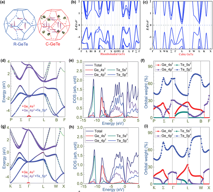 |
| | Fig. 3 (a) Calculated Fermi surface of rhombohedral and cubic GeTe with spin–orbital coupling (SOC).105 Calculated band structures for (b) rhombohedral GeTe and (c) cubic GeTe.106 Calculated band structures in orbital details for (c) rhombohedral GeTe and (g) cubic GeTe. Density of states and partial density of states of (d) rhombohedral GeTe and (h) cubic GeTe. Orbital weights for the highest occupied molecular orbital (HOMO) projected along the high symmetric points for (f) rhombohedral GeTe and (i) cubic GeTe.89 | |
In order to further study the band characteristics of GeTe, Fig. 3d–i show the influence of molecular orbitals (Ge_4s2, Ge_4p2, Te_5s2, and Te_5p4) with different orbital masses on the band structure.89 Similar to the case of GeTe molecular orbitals, Ge_4p2 and Te_5p4 occupy the lowest unoccupied molecular orbitals and the highest occupied molecular orbitals, while the Te_5s2 orbital mainly contributes to the subvalence band energy level. The Ge_4s2 orbital exists at L and Σ points and contributes to more orbital characters at the L point than at the Σ point as shown in Fig. 3f and i. This accounts for the higher energy in the L valence band. The stereochemically “expressed” Ge_4s2 lone-pair electrons in rhombohedral phase GeTe are related to the strong s–p orbital hybridization, inducing a significant distortion in the electron distribution. With increasing temperature, the lone electron pair of Ge_4s2 is quenched, reducing the effect on electron structural distortion and leading to a high symmetry structure.99,108 At the same time, the L band becomes the valence band maximum, which is consistent with the findings for the cubic PbTe and SnTe.
2.3 Phonon transport and lattice thermal conductivity
Lattice thermal conductivity, as a part of thermal conductivity, is an important and interdependent factor in evaluating the figure of merit ZT value, which is dominated by the phonon transport behaviors. In order to understand the thermal transport properties of rhombohedral and cubic GeTe, the phonon dispersion of these two phases is carefully studied. Wdowik et al.109 investigated the lattice dynamics and phonon transport of GeTe through density functional theory calculations as shown in Fig. 4a and b. Rhombohedral GeTe exhibits 6 phonon modes at Γ. The three lowest dispersions are acoustic modes, indexed as in-plane transverse acoustic mode (TA), in-plane longitudinal acoustic mode (LA) and out-of-plane flexural acoustic mode (ZA). The phonons belonging to the other three optical modes (two types of transverse optical modes (TO) and one longitudinal optical mode (LO)) show higher eigenvalues, leading to the separation of the acoustic and optical branches. Several imaginary modes are shown in the phonon dispersion of cubic GeTe, indicating its thermodynamic instability and absence at room temperature. Cubic GeTe shows the primary soft mode at the Γ point. Rhombohedral GeTe instead represents real frequencies across the Brillouin zone instead. According to the calculated phonon density of states and the results of the 125Te nuclear inelastic scattering experiment performed on GeTe, the vibration of the Ge sublattice dominates the highest frequency region composed of the LO-phonon band, while both the acoustic mode and the TO mode are related to the mixed vibration of the Ge and Te sublattice.109
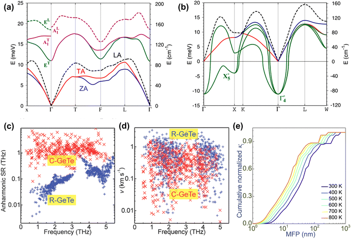 |
| | Fig. 4 Phonon-dispersion relations for (a) rhombohedral GeTe and (b) cubic GeTe at 300 K.109 (c) Anharmonic scattering rates (SRs) for rhombohedral and cubic GeTe at 300 K. (d) Group velocity (v) for rhombohedral and cubic GeTe at 300 K.23 (e) Normalized cumulative lattice thermal conductivity as a function of phonon MFP.30 | |
Fig. 4c shows the anharmonic scattering rates of rhombohedral and cubic GeTe.23 It can be seen that the anharmonic scattering rates are stronger in cubic GeTe, indicating the strengthened anharmonic phonon–phonon interaction. The group velocity of phonons is another key factor that determines the lattice thermal conductivity.110 Overall, the phonon group velocity in cubic GeTe is lower than that in rhombohedral GeTe (Fig. 4d), which is attributed to the higher coordination number and longer Ge–Te bonds in cubic GeTe than in rhombohedral GeTe. As a result, cubic GeTe has higher anharmonic scattering rates and a lower lattice thermal conductivity. The lattice thermal conductivity value is reduced from 2.6 W m−1 K−1 for rhombohedral GeTe at 300 K to 0.8 W m−1 K−1 for cubic GeTe at 700 K.111 According to the research by Chen et al., compared to the tellurides of the same main group (PbTe and SnTe), GeTe has a similar sound velocity but a lower average atomic mass; however, they still exhibit similar lattice thermal conductivity values.112 This phenomenon can be ascribed to the fluctuation in bond length caused by the symmetry breaking (cubic to rhombohedral GeTe), leading to fluctuations in the inter-atom force constant. Due to the relationship between the sound velocity and the force constant
where
vs is the sound velocity,
F is the force constant, and
M is the atomic mass, the sound velocity of rhombohedral GeTe (∼2100 m s
−1)
113 is comparable to that of cubic SnTe (∼2070 m s
−1).
114 The existence of the soft mode in the phonon density of states in GeTe results in the low mean free path of phonons. It is also noted that the mean free path of phonons is calculated to be 1–100 nm (
Fig. 4e),
30 which provides useful insights for further reduction in the lattice thermal conductivity of GeTe.
3. Tuning the electrical transport properties
Due to the large number of Ge vacancies, the pure GeTe sample has a high carrier concentration (∼1021 cm−3), a low Seebeck coefficient (∼30 μV K−1) and a moderate carrier mobility (∼50 cm2 V−1 s−1).18 Therefore, it is critical to optimize these parameters appropriately, which is crucial to improve the thermoelectric performance of the GeTe system. The Seebeck coefficient can be described by the Bethe-Summerfield expansion:115| |  | (6) |
where kB is the Boltzmann constant and q is the carrier charge. The Seebeck coefficient can be improved by lowering the carrier concentration due to the inverse relationship between the Seebeck coefficient and the carrier concentration, by inducing band convergence or the resonant level due to the dependence of the Seebeck coefficient on the symmetry breaking of density of states at the Fermi level and by introducing energy filtering since the second term (dμ(E)/dE) of the equation is associated with the scattering exponent (r). In addition, the phonon-drag effect is also reported to play an important role in improving the Seebeck coefficient at low temperatures. However, because GeTe is a mid-temperature thermoelectric material, it is usually assumed that the phonon-drag effect provides limited contributions.
3.1 Modulation of the band structure
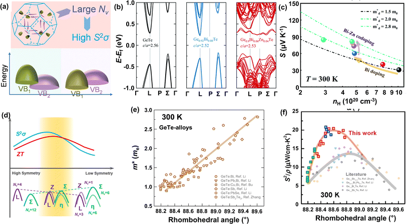
3.1.1 Band convergence.
Band convergence, a type of strategy that reduces energy differences (ΔE) between multiple band edges, as shown in Fig. 5a, has been adopted to improve the electrical transport properties in multiple thermoelectric systems. According to the equations,68,117| |  | (7) |
| |  | (8) |
where kB is the Boltzmann constant, e is the electron charge, n is the charge carrier concentration,  is the density-of-states effective mass, Nv is the valence band degeneracy, and
  is the band effective mass. Basically, eqn (7) is the Pisarenko equation based on the Boltzmann's transport theory. The band degeneracy can be increased via the band convergence strategy by decreasing ΔE. As mentioned above, there is an energy gap between the L band and Σ band in rhombohedral GeTe. By introducing appropriate doping or alloying elements, ΔE can be reduced, leading to improved band degeneracy and hence the Seebeck coefficient (eqn (7) and (8)). Table 1 shows the band characteristics and electronic transport properties induced by different doping/alloying elements. It is evident that the majority of these dopants are transitional metals, while others belong to the group 15 metals and lanthanide elements. These elements have outer s-orbitals, which help to bond with electrons as they enter the GeTe crystal lattice. Zn-doped GeTe samples can be taken as an example. Upon the incorporation of the Zn atom into the crystal lattice, the outer s-orbital of the Zn atom forms covalent bonds with the anion elements. However, due to the lower energy level of the s orbitals of the Zn atom compared to that of the valence band edge, doping with Zn atoms leads to a reduction in energy of the valence band edge of GeTe, resulting in a decrease in ΔE. The band structure of (Bi and Zn) co-doped GeTe samples is shown in Fig. 5b, indicating that Zn doping induces valence band convergence by tuning s-orbital energy.116Fig. 5c shows the increased
  after Zn doping.
 |
| | Fig. 5 (a) Schematic view of the band degeneracy for better properties.77 (b) Calculated band structure of pristine GeTe, Ge0.92Bi0.08Te, and Ge0.9Bi0.06Zn0.04Te. (c) Carrier concentration-dependent Seebeck coefficient for Ge1−xBixTe and Ge0.94−yBi0.06ZnyTe samples at 300 K.116 (d) Schematic of symmetry reduction for better band degeneracy. (e) Density-of-states effective mass  versus the rhombohedral angle (α) for GeTe-alloys at 300 K.72 (f) Power factor versus the rhombohedral angle (α) for GeTe-alloys at 300 K.51 versus the rhombohedral angle (α) for GeTe-alloys at 300 K.72 (f) Power factor versus the rhombohedral angle (α) for GeTe-alloys at 300 K.51 | |
Table 1 Electrical properties of GeTe samples with different dopants
| Dopants |
Compositions |
ΔEL–Σ (eV) |
S
max (μV K−1) |
PFmax (μW cm−1 K−2) |
ZT
max
|
| Bi47 |
Ge0.94Bi0.05Te |
0.074 |
226.5 |
40 |
∼1.7 |
| Bi116 |
Ge0.92Bi0.08Te |
0.13 |
238 |
27 |
∼1.5 |
| Bi–Zn116 |
Ge0.9Bi0.06Zn0.04Te |
0.03 |
240 |
33 |
∼2.0 |
| Bi–Mg32 |
Ge0.94Mg0.04Bi0.06Te |
0.06 |
254 |
54 |
2.5 |
| Bi–Sb16 |
Ge0.85Bi0.05Sb0.1Te |
0.151 |
208 |
∼37 |
1.8 |
| Pb118 |
Ge0.816Pb0.144Bi0.05Te |
0.077 |
238 |
32.7 |
∼2.0 |
| Bi–Pb26 |
Ge0.87Pb0.13Te–3% Bi2Te3 |
0.08 |
275 |
35.2 |
∼1.9 |
| V119 |
Ge0.98V0.02Te |
0 |
178 |
44 |
1.26 |
| Cd120 |
Ge0.97Cd0.03Te |
0.08 |
170 |
45 |
1.4 |
| Ti121 |
Ge0.97Ti0.03Te |
0.11 |
203 |
27 |
∼1.2 |
| Sb–Zn77 |
Ge0.86Sb0.1Zn0.04Te |
0.01 |
247 |
39 |
2.3 |
| Mn–Sb122 |
Ge0.85Mn0.05Sb0.08Te |
0.09 |
205 |
33.61 |
1.67 |
| Mn123 |
Ge0.94Mn0.06Te |
0.01 |
110 |
28 |
0.55 |
3.1.2 Symmetry modulation.
As discussed above, there is symmetry evolution when the temperature is elevated, accompanied by the change in the energy difference of bands, especially for L and Σ bands. This phenomenon offers a new insight to increase the Nv. Li et al. successfully fabricated a series of GeTe-based thermoelectric materials by regulating the contents of Pb and Bi (Ge1−x−yPbxBiyTe). Ge0.86Pb0.1Bi0.04Te reached an intermediate rhombohedral state before transferring to a cubic phase. This intermediate state showed an exceptionally high ZT value of ∼2.4 at 600 K; this value was the highest ZT value in 2018. Such a material also exhibited a very high average ZT of 1.3 in the range of 300–600 K. This phenomenon can be ascribed to the fact that by yielding an Nv close to 16 in the intermediate state, the density of states effective mass can be conspicuously increased when the multiple valence band edges are well aligned. The degree of structure symmetry can be evaluated using the rhombohedral angle (Fig. 5d). Fig. 5e shows the relationship between the density of states effective mass and the rhombohedral angle.72 It can be seen that there is almost a linear relationship between these two parameters. The density of states effective mass increases with an increasing rhombohedral angle. As shown in Fig. 5f, the power factor shows an upward trend followed by a decrease as a function of the rhombohedral angle.51 The optimal rhombohedral angle ranges from 88.5° to 89.0°, with a corresponding  of 1.2–1.9m0. It is reasonable to select promising GeTe-based thermoelectric materials within an appropriate rhombohedral phase angle. Such materials are foreseen to exhibit exceptional electrical performance.
3.1.3 Introduction of the resonant level.
Introducing resonant energy states was first proposed in PbTe by Heremans et al.75 By doping Tl, they reported a significantly improved Seebeck coefficient through the distortion of the electronic density of states near the Fermi level, namely resonant levels (Fig. 6a). The core concept of this strategy is to increase the energy-dependence of n(E) near the Fermi level, so as to increase the density-of-states effective mass. The distortion of the band structure greatly increases the Seebeck coefficient without sacrificing the electrical conductivity, and thus the PF can be improved. Such a strategy is also applicable to GeTe systems. Through DFT calculations, it is found that the resonant level can be introduced into the valence band in both rhombohedral and cubic GeTe by In or Ga doping, as shown in Fig. 6b and c.124 It is clear that there is an abrupt increase near the Fermi level in the DOS of In-doped and Ga-doped GeTe, induced by orbital hybridization between In/Ga and the host atom. The Seebeck coefficient shows an increase after In doping, especially near room temperature (Fig. 6d). As shown in Fig. 6e, the data points of the In-doped GeTe samples deviate largely from the Pisarenco curve, indicating improved density-of-states effective mass; the In doped GeTe samples show a high ZT as a result (Fig. 6f).23,27,124,125 For Ga doping, Zhang et al. found that the grain boundary complexions were formed by Ga segregation or Ga2Te3.46 The role of Ga doping in inducing the resonant level may not be expressed in GeTe samples.
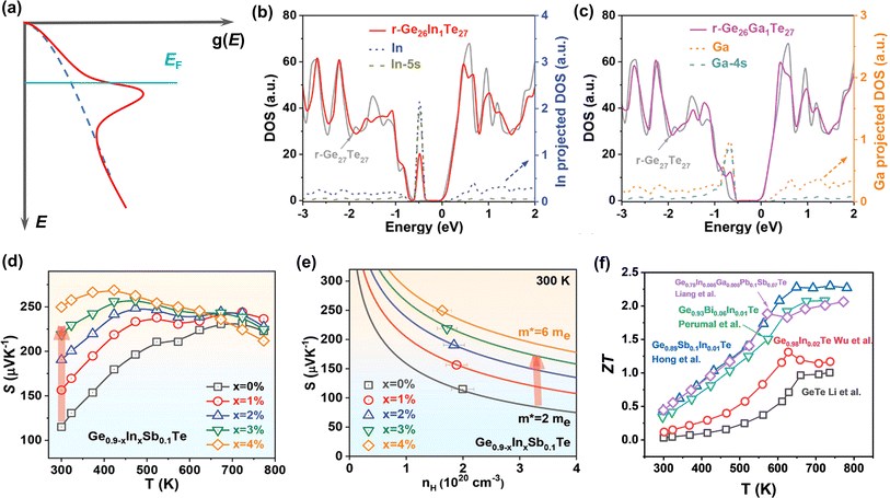 |
| | Fig. 6 (a) Schematic view of the distortion of the band structure induced by the resonant level. The total DOS and projected DOS for (b) r-Ge26In1Te27 and (c) r-Ge26Ga1Te27. (d) Temperature-dependent Seebeck coefficient for Ge0.9−xInxSb0.1Te. (e) Hall carrier concentration-dependent Seebeck coefficient at 300 K. (f) The temperature-dependent ZT value for In doped GeTe samples.23,27,124,125 | |
3.1.4 Rashba effect.
The Rashba spin-splitting effect generates a distinct constant density of states (DOS) near the Fermi level. This effect can enhance band degeneracy, reinforce anharmonicity and introduce soft bond simultaneously, leading to a high Seebeck coefficient and low lattice thermal conductivity.126 In non-centrosymmetric materials, strong spin–orbit coupling (SOC) can induce the Rashba effect, resulting in the splitting of a single energy band edge into two band extrema with energy shift and momentum offset (Fig. 7a). GeTe, undergoing a phase transition near 700 K that breaks the inversion symmetry, also exhibits the Rashba effect. In rhombohedral GeTe, the displacement of Te atoms from their central positions enhances Rashba energy ER and momentum offset k0. The energy dispersion relation near the extrema point of spin-degenerate parabolic band can be described by the band effective mass  approximation:
| | 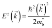 | (9) |
while the two spin-polarized bands are described by| |  | (10) |
where E is the energy dispersion with the superscript ± representing the spin polarizations, k is the momentum, and αR is the Rashba parameter:127| |  | (11) |
 |
| | Fig. 7 (a) Schematic views of the spin-degenerated and spin-dependent shift of the energy dispersion caused by the Rashba effect. (b) Calculated curves of the Seebeck coefficient as a function of the Hall carrier concentration for Ge1−x−ySnxSbyTe at 300 K. Calculated band structures of rhombohedral (c) Ge64Te64 and (d) Ge61Sn3Te64.30 | |
Notably, Hong et al. found that  increased at both 300 K and 780 K, indicating an improved Seebeck coefficient (Fig. 7b). According to the DFT calculations, the Rashba spin-splitting effect could be enhanced in the band structure of GeTe through Sn doping, thereby elevating the energy level of valence band edges near point Z (Fig. 7c and d).30
3.2 Defect engineering in carrier concentration
The role of the carrier concentration is critical, affecting the Seebeck coefficient, electrical conductivity and electronic thermal conductivity. In semiconductors, the number of defects can directly affect the carrier concentration. Therefore, understanding the characteristics of defects and origins of the high carrier concentration in GeTe will benefit the performance modulation.
The formation energies of potential defects in GeTe, including the antisite defect of Ge at the Te site (GeTe), the antisite defect of Te at the Ge site (TeGe), the Te vacancy (VTe), and the Ge vacancy (VGe), can be calculated using DFT. As shown in Fig. 8a–d, VGe has the lowest defect formation energy in both rhombohedral and cubic GeTe, indicating that the Ge vacancy is the dominant defect in GeTe.129,130 According to the defect reaction equation
| | 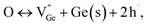 | (12) |
it can be seen that the formation of one Ge vacancy is accompanied by the presence of two holes. In pure GeTe, the fraction of Ge vacancies is about 2.5 at%, corresponding to a carrier concentration of about 10
21 cm
−3. It is also worth noting that the Ge vacancy in rhombohedral GeTe has a lower formation energy than in cubic GeTe, indicating a much higher carrier concentration in the cubic phase. According to the calculated DOS for Ge
64−xTe
64 (
x = 0, 1, 2 and 3), the Fermi level shifts towards the valence band with increasing
x, supporting the increased carrier concentration as well (
Fig. 7b).
128
 |
| | Fig. 8 (a) Schematic view of Ge vacancies in the GeTe matrix. (b) DOS for rhombohedral Ge64−xTe64 with different amounts of Ge deficiencies.128 The formation energy of atomic defects in (c) cubic and (d) rhombohedral GeTe as a function of the relative Fermi-energy under Ge-rich conditions.129 | |
The optimal carrier concentration for GeTe is determined to be 1 − 2 × 1020 cm−3 by theoretical calculation and analysis. Based on the previous studies, the methods for optimizing the carrier concentration can be roughly classified into three categories. Donor doping turns out to be an effective strategy to reduce the carrier concentration (Fig. 9a). The dopants at cation sites, such as Bi,18,47 Sb,19,131 Sc,29 Y,132etc., proved to be effective donors (Fig. 9b), contributing to the improvement of the Seebeck coefficient and PF. For example, compared to the Ge2+ ions, Bi, Sb, Sc, and Y have a valence of +3. When these elements enter the GeTe lattice, they can provide electrons to decrease the hole concentration. Considering Bi and Sb doping as an example, following the defect reaction:
| |  | (13) |
| |  | (14) |
the hole concentration decreased from ∼8.72 × 10
20 cm
−3 for pristine GeTe to ∼1 × 10
20 cm
−3 for the Ge
0.92Bi
0.08Te sample and ∼2.38 × 10
20 cm
−3 for the Ge
0.9Sb
0.1Te sample at 300 K (
Fig. 9b). The Seebeck coefficient increases from ∼30 μV K
−1 for the un-doped GeTe sample to ∼160 μV K
−1 for the Ge
0.92Bi
0.08Te sample at 300 K.
18,91 As for Sc doping, the hole concentration decreased from ∼8.6 × 10
20 cm
−3 for pristine GeTe to ∼3.2 × 10
20 cm
−3 and ∼2.1 × 10
20 cm
−3 for the Ge
0.98Sc
0.02Te sample and the Ge
0.94Sc
0.06Te sample, respectively. The Seebeck coefficient increases from 36.6 to 86.1 μV K
−1. It can be seen that there are differences in carrier mobility for samples with different dopants.
29 By Sc and Y doping, negligible variations in

are observed, but the carrier mobility shows an upward trend; for Bi and Sb doping,

is improved, whilst the carrier mobility suffers from degradation as shown in
Fig. 9b and c. The underlying mechanism will be discussed later.
 |
| | Fig. 9 (a) Schematic view of the donor doping method for reducing the carrier concentration. Hall carrier concentration-dependent (b) Seebeck coefficient and (c) carrier mobility at 300 K for Bi-doped,18,47 Sb-doped,19,131 Sc-doped29 and Y-doped132 GeTe samples. (d) The defect formation energy of different point defects for pristine GeTe, (GeTe)1−x(PbSe)x, and Ge1−xSb2/3xTe. The inset image shows the schematic view of the improved defect formation energy for decreasing carrier concentration. Hall carrier concentration-dependent (e) Seebeck coefficient and (f) carrier mobility at 300 K for (GeTe)1−x(PbSe)x,113 Ge1−xSb2/3xTe24 samples. (g) Schematic view of the lattice plainification method for reducing carrier concentration. Hall carrier concentration-dependent (h) Seebeck coefficient and (i) carrier mobility at 300 K for Cu-doped51 and Ge self-doped GeTe samples.28 | |
Secondly, the carrier concentration can be optimized by elevating the defect formation energy of Ge vacancies. For the GeTe–PbSe alloys,113 namely (GeTe)1−x(PbSe)x, it was found that the formation energy of Ge vacancies increased gradually with increasing PbSe content through DFT calculations (Fig. 9d). The formation energies of Ge vacancies in (GeTe)1−x(PbSe)x samples gradually increased from 0.5 eV to 0.79 eV. The concentration of Ge vacancies decreased and the solubility of Ge precipitates increased. As a result, the carrier concentration of the (GeTe)1−x(PbSe)x samples was reduced from 7.8 × 1020 cm−3 (x = 0) to 0.8 × 1020 cm−3 (x = 0.4) as shown in Fig. 9e. Basically, compared to Ge2+ (0.76 nm) and Te2− (2.21 nm), the ionic radius of Pb2+ is larger (1.13 nm), while the anion radius of Se2− is smaller (1.96 nm). Therefore, alloying with PbSe increases the size of the cation and decreases the size of the anion, favorable for reducing the concentration of cation vacancies. The alloying of Sb2Te3 is similar to that of PbSe. Considering the valence state and substitution of additive Sb3+, the reduced carrier concentration cannot be attributed to the donor effect. The defect reaction equation is shown as follows:
| |  | (15) |
DFT calculation results provide evidence for increased formation energy of Ge vacancies, accounting for the reduced carrier concentration.24Fig. 9f indicates the deteriorated carrier mobility with an increasing doping level due to the introduction of a number of extrinsic atoms.
Thirdly, lattice plainification is also effective in optimizing the carrier concentration and improving carrier mobility (Fig. 9g). In GeTe, Cu doping or Cu2Te alloying is considered popular. By alloying only 1.5% Cu2Te, the carrier concentration in GeTe is reduced from ∼8 × 1020 cm−3 to ∼2 × 1020 cm−3 and the carrier mobility is increased to over 130 cm2 V−1 s−1 as shown in Fig. 9h and i. To unveil the mechanism, Bu et al. carried out DFT calculations,51 which suggested that the GeTe–Cu2Te alloys involve both substitutions and interstitials, leading to a charge compensation. The reduction in the carrier concentration can be attributed to the re-dissolution of Ge precipitates, suggesting that the Ge atoms enter the GeTe lattice and refill the vacancy. To suppress the Ge deficiency, Dong et al.28 optimized the amount of excessive Ge (Ge1+xTe) by mechanical alloying combined with spark plasma sintering, and a reduction in the carrier concentration from 8 × 1020 cm−3 to ∼3 × 1020 cm−3 was achieved. A high Seebeck coefficient value of more than 60 μV K−1 was realized in pristine GeTe at room temperature. Due to the suppressed carriers interaction and lack of Ge vacancies, the carrier mobility was elevated to ∼90 cm2 V−1 s−1. Therefore, a high PF close to ∼24 μW cm−1 K−2 was obtained at room temperature. Lyu et al.133 reported that through AgCuTe alloying, excessive Ge participated in the defect reaction and re-dissolved into the lattice, thereby decreasing the enrichment of Ge and diminishing the carrier concentration. The defect reaction equation is shown as follows:
| |  | (16) |
The carrier concentration decreased from ∼2.8 × 1020 cm−3 to ∼1.0 × 1020 cm−3 at 300 K. The Seebeck coefficient increased from 86.29 μV K−1 to 167.68 μV K−1 at 300 K. A high power factor of 18.58 μW cm−1 K−2 was achieved. Yin et al.134 recently reported that interstitial Cu plays an important role in improving thermoelectric performance. Interstitial Cu can also reduce the carrier concentration in GeTe. Cu doping also improves the carrier mobility to around 100 cm2 V−1 s−1, compared to the value of about 40 cm2 V−1 s−1 in pristine GeTe.
3.3 Other strategies
3.3.1 Energy filtering effect.
The energy filtering effect can effectively improve the electrical transport properties of thermoelectric materials.135 Generally, by introducing various inclusions or nanostructures, such as nanoparticles, nanopores, heterostructures and superlattices, interfacial potential barriers will contribute differently to scattering high-energy and low-energy charge carriers. Charge carrier energy band bending at metal–semiconductor or semiconductor–semiconductor interfaces can be constructed. This band bending acts as a slowly varying potential, which strongly scatters low-energy charge carriers (Fig. 10a). Composite design can strengthen carrier scattering due to the formation of heterogeneous interfaces. To optimize the electrical transport properties, the composites should match the following physical properties:135 (i) the size of impurities comparable to the mean free path of carriers, (ii) the close band gap and/or work function between the matrix materials and the impurities, and (iii) the impurities located along the grain boundaries. When these conditions are well satisfied, the correct barrier height can be ensured, which can effectively scatter low-energy charge carriers. Jiang et al.47 optimized carrier scattering in GeTe samples by introducing boron inclusions (Fig. 10b). The S ∼ nH relationship of the boron-added samples exhibited deviations from the Pisarenco curves, which was attributed to the enhanced scattering factors after adding boron, indicating that boron/GeTe heterogeneous interfaces proved to be effective in carrier scattering as shown in Fig. 10c. This phenomenon significantly improved both the Seebeck coefficient and the power factor (PF). The Seebeck coefficient was improved from ∼83.14 μV K−1 for the pristine sample to ∼97.3 μV K−1 for samples incorporated with 0.4 wt% boron at room temperature. The power factor was improved to 25.4 μW cm−1 K−2 at room temperature and reached 47.7 μW cm−1 K−2 at 573 K (Fig. 10d). This effect helps prevent a significant decrease in electrical conductivity while promoting an increase in the Seebeck coefficient, ultimately aiming to enhance the power factor. Levin et al.10 found that the increased Seebeck coefficient in Dy-doped Ag6.52Sb6.52Ge36.96Te50 (acronym TAGS-85), one of the GeTe derivatives alloyed with AgSbTe2 ((GeTe)x(AgSbTe2)100−x), could also be ascribed to the energy filtering effect. The results of X-ray diffraction and 125Te nuclear magnetic resonance spectroscopy showed that Dy atoms were incorporated into the GeTe lattice. Due to the large atomic size and high magnetic moment, the Dy atom impeded the transport of low-energy charge carriers, thereby improving the Seebeck coefficient and power factor. The Seebeck coefficient was improved from ∼77 μV K−1 for the TAGS-85 sample to ∼96 μV K−1 for TAGS-85 doped with a 1% Dy sample at room temperature (Fig. 10e). The power factor was improved to 16 μW cm−1 K−2 at room temperature and reached 35 μW cm−1 K−2 at 540 K (Fig. 10f).
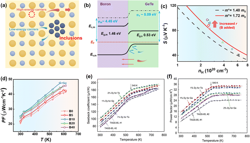 |
| | Fig. 10 (a) Schematic view of blocking parts of carriers by introducing inclusions. (b) Schematic view of potential barriers at the interfaces between boron and GeTe. (c) Hall carrier concentration-dependent Seebeck coefficient at 300 K for boron-added samples. (d) Temperature-dependent power factor for boron-added samples. Temperature-dependent (e) Seebeck coefficient and (f) power factor of Ag6.52Sb6.52Ge36.96Te50 (TAGS-85) with and without Dy doping. | |
3.3.2 Directional defect evolution.
Due to the significant amount of Ge vacancies present in GeTe, the scattering of holes caused by Ge vacancies is inevitable, leading to a reduction in carrier mobility. As mentioned above, some strategies can reduce the defect formation energy or act as interstitial atoms to improve the carrier mobility. Is it possible to develop a rational fabrication route to weaken the scattering effect of Ge vacancies?
Owing to structural considerations, the number of Ge vacancies in the cubic phase is larger than that in the rhombohedral phase. Zhang et al.129 annealed SPSed GeTe samples at 623 K and 773 K with different time durations, respectively. The morphology is shown in Fig. 11a–d. They found that the samples annealed at 623 K showed much lower Ge vacancies and carrier concentration, resulting in an enhanced Seebeck coefficient and PF. Fig. 11e shows that the carrier concentration was reduced from ∼10.5 × 10²⁰ to ∼3 × 1020 cm−3 after annealing for 2 days at 623 K, and this value was maintained after 7-day annealing. The Seebeck coefficient increased from 30 μV K−1 to 70 μV K−1 at 300 K, while PF values increased from ∼7 μW cm−1 K−2 to ∼27.5 μW cm−1 K−2 at 300 K (Fig. 11f). Surprisingly, the carrier mobility was elevated to an extremely high value of 150 cm2 V−1 s−1. The cubic phase shows much lower formation energy, leading to higher Ge vacancies. GeTe samples undergo a transformation from cubic into a rhombohedral phase during the cooling-down process after sintering, and vacancies are maintained. By appropriately annealing, excess supersaturated vacancies can be eliminated, contributing to a low carrier concentration and high carrier mobility. Furthermore, Jiang et al.39 proposed a novel strategy to drive the defect evolution in GeTe (Fig. 11g). With the assistance of the high-temperature heat-treatment, supersaturated vacancies can be transformed into dense dislocations and hierarchical nano-domain structures with planar vacancies. This defect evolution can weaken the carrier scattering of Ge vacancies without affecting the carrier concentration. Tational heat treatment is effective in improving the carrier mobility, which breaks the conventional relationship of the Seebeck coefficient and electrical conductivity, resulting in a higher power factor. The Hall mobility for Bi0.07Ge0.90Te-873 reached 55.4 cm2 V−1 s−1, while a lower result of 41.1 cm2 V−1 s−1 was obtained for Bi0.07Ge0.90Te-723 as shown in Fig. 11h. Fig. 11e shows that a high PF of 45 μW cm−1 K−2 was obtained at 648 K for the Bi0.07Ge0.90Te-873 sample.
 |
| | Fig. 11 (a and b) SEM and (c and d) BSE images for GeTe ingots annealed at different temperatures, respectively. (e) The evolution of carrier concentration and carrier mobility for GeTe samples annealed at 773 and 623 K, respectively. (f) Temperature-dependent power factor for pristine and annealed GeTe samples.129 (g) The schematic diagram presenting the behaviors of carriers and phonons in the GeTe-based compounds with the presence of hierarchical structures. (h) Hall carrier concentration and carrier mobility for the BixGe0.97−xTe-723 and BixGe0.97−xTe-873 samples at room temperature. (i) Temperature-dependent power factor for BixGe0.97−xTe-723 and BixGe0.97−xTe-873 samples.39 | |
3.4 Insights from the weighted mobility
In the preceding three sections, we have enumerated numerous methods for optimizing the electrical transport properties of p-type GeTe materials. As depicted in Table 2, one dopant usually has multiple effects on the transport properties of GeTe. For instance, Bi doping can simultaneously reduce the carrier concentration and induce band convergence, but hinder carrier transport, thereby decreasing the carrier mobility. Cu doping can realize a reduction in the carrier concentration and improvement in carrier mobility. For In doping, distortion of density-of-states in the GeTe band structure and the reduced carrier concentration improve the Seebeck coefficient effectively. However, according to the equation:3| | 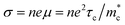 | (17) |
μ is proportional to the carrier relaxation time (τc) and inversely proportional to carrier effective mass  , which is related to the density-of-states effective mass. The introduced resonant level does harm to carrier mobility due to both the increased density-of-states effective mass and reduced carrier relaxation time. To facilitate comparison of performance differences and further exploration of their potential applications, weighted mobility was utilized to classify and compare the electrical properties and performance of these elements. Weighted mobility is a descriptor that directly evaluates electronic qualities.138 Furthermore, weighted mobility is a parameter as the electrical part in the equation describing the quality factor B, which is proportional to the ZT value.139,140 An intriguing observation emerged: some elements, such as Bi (shown in Fig. 12a), exhibited nearly constant or even decreased weighted mobility, while some others, such as Cu (shown in Fig. 12b) demonstrated a gradual increase in weighted mobility with increasing doping content at 300 K.
Table 2 Effect of different dopants on GeTe (units of PF at 300 K: μW cm−1 K−2)
| Dopants |
Band |
Rhombohedral angle |
Carrier concentration |
Carrier mobility |
PF |
| Bi |
Band convergence |
Increased |
Decreased |
Decreased |
∼10–16 (ref. 18) |
| Sb |
Band convergence |
Increased |
Decreased |
Decreased |
∼10–17 (ref. 19) |
| Zn |
Band convergence |
Increased |
Slightly decreased |
Decreased |
— |
| Pb |
Band convergence |
Increased |
Decreased |
Decreased |
∼10 (ref. 12) |
| V |
Band convergence |
— |
Decreased |
— |
∼12–15 (ref. 119) |
| Cd |
Band convergence |
Increased |
Slightly decreased |
Decreased |
∼9 (ref. 22) |
| Ti |
Band convergence |
Increased |
Slightly decreased |
Decreased |
∼11 (ref. 121) |
| Mn |
Band convergence |
Increased |
Increased |
Decreased |
<10 (ref. 123) |
| In |
Resonant level |
Increased |
Decreased |
Decreased |
∼14 (ref. 125) |
| Cu |
— |
Slightly increased |
Decreased |
Increased |
≥20 (ref. 52) |
| Sc |
— |
Slightly increased |
Decreased |
Increased |
23.3 (ref. 29) |
| Y |
— |
Slightly increased |
Decreased |
Increased |
19.1 (ref. 132) |
| Ge |
— |
— |
Decreased |
Increased |
∼24 (ref. 28) |
| Cr |
Improved md |
Slightly increased |
Decreased |
— |
∼15 (ref. 136) |
| Ag |
Improved md |
Decreased |
Increased |
Decreased |
<5 (ref. 137) |
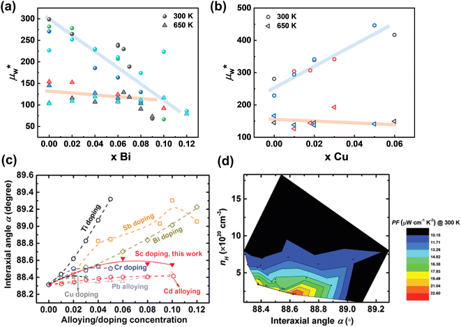 |
| | Fig. 12 The weighted mobility for (a) Bi-doped18,116,141,142 and (b) Cu-doped51,52,143 GeTe samples. (c) Rhombohedral angle α as a function of alloying or doping concentration. (d) Contour plot representation of the room-temperature power factor as a function of the rhombohedral angle (interaxial angle) α and Hall carrier concentration nH.29 | |
According to the equation:138
| |  | (18) |
where
μ0 is the draft mobility,
m* is the density-of-states effective mass and
me is the electron mass. It is apparent that weighted mobility comprises two components: carrier mobility and density-of-states effective mass. Samples with improved weighted mobility usually show a marked increase in carrier mobility. These dopants hardly change the rhombohedral angle, but decrease the concentration of Ge vacancies. A high power factor was achieved in these samples as shown in
Table 2 (such as Cu, Sc, Y and Ge). Conversely, those with unchanged or reduced weighted mobility display decreased carrier mobility but an increased density-of-states effective mass—a phenomenon indicating contributions from the band convergence. The offsetting effect between the reduced carrier mobility and increased density-of-states effective mass results in only marginal improvements in the weighted mobility and power factor for these samples.
Subsequently, it is important to establish a relationship between the structure and electrical properties. As mentioned previously, band convergence inevitably brings structural changes—particularly alterations in rhombohedral angles. Upon comparing data on the rhombohedral angle with the power factor for these samples, it can be observed that within an optimal range of rhombohedral angle values, the power factor reached higher values (Fig. 12c and d).29 This is attributed to the fact that the rhombohedral angle reflects the symmetry of the pseudo-cubic structure. On one hand, as this angle approaches 90° (indicating a tendency toward a cubic structure), there is an increase in Ge vacancies due to lower formation energy in cubic GeTe. The carrier scattering is strengthened by Ge vacancies with a higher concentration and the alloying atoms. On the other hand, there is an optimal rhombohedral angle value suggested by Zhang et al.,72 corresponding to the variation of temperature-dependent ΔE between L and Σ bands. Therefore, it is imperative to consider the rhombohedral angle while selecting suitable dopants and their content; this helps maintain high levels of weighted mobility, thereby enabling a higher power factor, especially near room temperature.
3.5 Insights into n-type GeTe
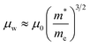
To realize the transition from p-type to n-type GeTe, the defect chemistry should be focused on—the high intrinsic Ge vacancies contribute to a high hole concentration, making it difficult to realize n-type GeTe144,145 (Fig. 13a). Samanta et al.147 reported a high ZT value of ∼0.6 at 500 K in n-type GeTe by alloying AgBiSe2 ((GeTe)100−x(AgBiSe2)x). It shows two distinct regions in the compositional variation dependent band gap, electrical conductivity and Seebeck coefficient. By increasing the AgBiSe2 concentration up to ∼20%, the band gap decreases from ∼0.18 eV to near 0 eV. Then the band gap starts to increase to 0.25 eV at x = 50 (Fig. 13b). The electrical conductivity decreases at first due to the reduced hole concentration and starts to increase slightly with the increasing AgBiSe2 concentration (Fig. 13c). The Seebeck coefficient starts to increase from ∼34 μV K−1 to ∼392 μV K−1 up to x = 25, followed by a sudden change to −278 μV K−1 at x = 30 (Fig. 13d). From the view of the band structure, the conduction band edge is dominated by Ge p orbitals in pristine GeTe. By alloying AgBiSe2, the Bi3+ substitution for Ge2+ strongly contributes to the conduction band edge states. Wang et al.146 reported that by reducing the formation energy of Te vacancies via AgBiTe2 alloying, the electron concentration was optimized, boosting the power factor to 6.2 μW cm−1 K−2. Fig. 13e shows the power factor of n-type GeTe-based thermoelectric materials, compared to the high power factor in p-type GeTe; this indicates that there is still plenty of scope for further optimization.
 |
| | Fig. 13 (a) Schematic diagram of p-type GeTe conversion to n-type.146 Compositional variation of (b) band gap, (c) electrical conductivity, and (d) Seebeck coefficient with the AgBiSe2 concentration in (GeTe)100−x(AgBiSe2)x (x = 0–50) at room temperature. (e) Comparison of S2σ of some representative n-type GeTe-based thermoelectric materials.147 | |
4. Lowering lattice thermal conductivity
In addition to optimization of electrical transport performance, regulating thermal conductivity is also important for enhancing ZT values.148 In GeTe, the total thermal conductivity can be described as:
The electronic thermal conductivity was calculated using the Wiedemann–Franz law:149,150
where the Lorenz factor (
L) was estimated using the single parabolic band (SPB) model. It is easily understood that the electronic thermal conductivity can be reduced as a natural consequence of reduced carrier concentration especially in GeTe. However, the lattice thermal conductivity is a relatively independent factor; inhibiting phonon transport is beneficial for optimizing the thermoelectric performance of GeTe materials. The mechanisms of phonon scattering mainly involve phonon–phonon scattering (umklapp processes
151), point defect scattering (zero-dimension (0D) defects
152,153), dislocation scattering (one-dimension (1D) defects
154), interface scattering (two-dimension (2D) defects
155), and precipitate scattering (three-dimension (3D) defects
156,157) (
Fig. 14). The lattice thermal conductivity can be described in the form of relaxation time:
158,159| |  | (21) |
where
νs is the average sound speed,
ℏ is the reduced Planck constant,
θD is the Debye temperature,
z =
ℏω/
kBT, representing the reduced phonon frequency (
ω denotes the phonon frequency), and
τtot is the total relaxation time that is further described as:
| | | τtot−1 = τU−1 + τGB−1 + τDB−1 + τPD−1 + τPV−1 + τSF−1 + τD−1 + τNP−1 + ⋯ | (22) |
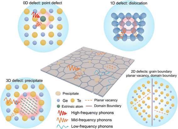 |
| | Fig. 14 Microstructure engineering for reducing lattice thermal conductivity. Schematic view for different types of phonon scattering sources in GeTe. | |
The total relaxation time is contributed from various mechanisms such as the umklapp (U) processes, grain boundary (GB), domain boundary (DB), point defects (PDs), planar vacancy (PV), stacking fault (SF), dislocation (D), and nanoprecipitate (NP) according to Matthiessen's equation (eqn (22)). Different scattering sources aim at phonons with different wavelengths or frequencies. Therefore, the establishment of all-scale hierarchical structures often requires the participation of various defects (Fig. 14). Many efforts have been devoted to lowering the lattice thermal conductivity in recent years as shown in Fig. 15. This section will classify the defects in GeTe-based thermoelectric materials into different dimensions.
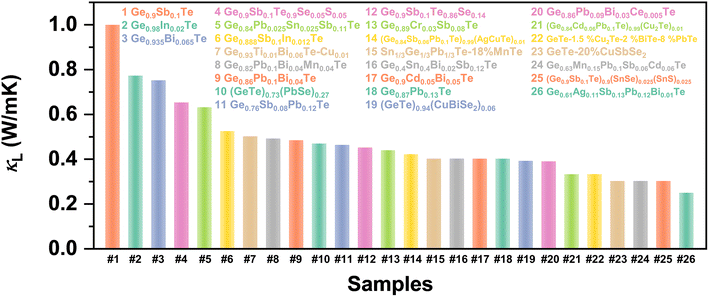 |
| | Fig. 15 Summary of reported minimum lattice thermal conductivity in Ge0.9Sb0.1Te,19 Ge0.98In0.02Te,125 Ge0.935Bi0.065Te,18 Ge0.9Sb0.1Te0.9Se0.05S0.05,17 Ge0.84Pb0.025Sn0.025Sb0.11Te,45 Ge0.888Sb0.1In0.012Te,23 Ge0.93Ti0.01Bi0.06Te–Cu0.01,134 Ge0.82Pb0.1Bi0.04Mn0.04Te,37 Ge0.86Pb0.1Bi0.04Te,25 (GeTe)0.73(PbSe)0.27,113 Ge0.76Sb0.08Pb0.12Te,21 Ge0.9Sb0.1Te0.86Se0.14,19 Ge0.89Cr0.03Sb0.08Te,128 (Ge0.84Sb0.06Pb0.1Te)0.99(AgCuTe)0.01,160 Sn1/3Ge1/3Pb1/3Te–18% MnTe,161 Ge0.4Sn0.4Bi0.02Sb0.12Te,162 Ge0.9Cd0.05Bi0.05Te,22 Ge0.87Pb0.13Te,11 (GeTe)0.94(CuBiSe2)0.06,163 Ge0.86Pb0.09Bi0.03Ce0.005Te,164 (Ge0.84Cd0.06Pb0.1Te)0.99(Cu2Te)0.01,50 GeTe–1.5% Cu2Te–2% BiTe–8% PbTe,51 GeTe–20% CuSbSe2,49 Ge0.63Mn0.15Pb0.1Sb0.06Cd0.06Te,36 (Ge0.9Sb0.1Te)0.9(SnSe)0.025(SnS)0.025,165 and Ge0.61Ag0.11Sb0.13Pb0.12Bi0.01Te.38 | |
4.1. 0D defects
Point defects usually originate from missing atoms or irregular atomic replacement, such as vacancies, antisite defects, interstitials, and substitutional atoms (Fig. 16a). Besides intrinsic defects, dopants can also serve as point defects to scatter high-frequency phonons, which are commonly adopted to lower lattice thermal conductivity in GeTe-based thermoelectric materials. The scattering effect on high-frequency phonons can be observed through the relationship between relaxation time and phonon frequency:167,168| | 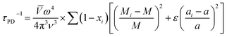 | (23) |
where ν is the Poisson ratio, ![[V with combining macron]](https://www.rsc.org/images/entities/i_char_0056_0304.gif) is the average atomic volume,
is the average atomic volume, ![[M with combining macron]](https://www.rsc.org/images/entities/i_char_004d_0304.gif) is the average atomic mass, and ε is the phenomenological parameter. The intensity of point defect scattering can be estimated using the mass scattering parameter (ΓM) and strain scattering parameter (ΓS). The scattering parameters can be described as
is the average atomic mass, and ε is the phenomenological parameter. The intensity of point defect scattering can be estimated using the mass scattering parameter (ΓM) and strain scattering parameter (ΓS). The scattering parameters can be described as| | 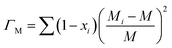 | (24) |
and55| |  | (25) |
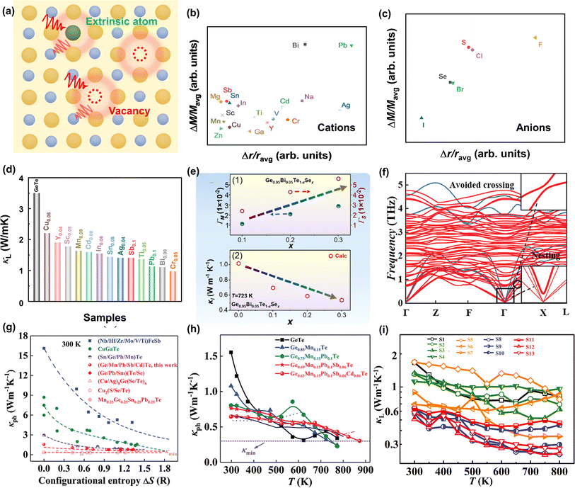 |
| | Fig. 16 (a) The schematic view for point defects. The mass fluctuation and strain field fluctuation of dopants in GeTe: (b) dopants at the cation site and (c) dopants at the anion site. (d) The lattice thermal conductivity of GeTe-based compounds doped with typical elements.18,19,22,29,30,121,123,125,128,132,137. (e1) Calculated composition-dependent ΓM and ΓS of Ge0.95Bi0.05Te1−xSex as a function of Se content. (e2) Predicted composition-dependent lattice thermal conductivity of Ge0.95Bi0.05Te1−xSex at 723 K.166 (f) Phonon dispersion spectra of pristine GeTe (blue lines) and GeTe co-doped with Pb and Bi (red lines). The insets show a zoom-in of avoided crossing behavior and nesting.164 (g) Lattice thermal conductivity as a function of ΔS for GeTe-based alloys at room temperature.36 (h) Temperature-dependent lattice thermal conductivity for medium-entropy alloyed GeTe samples. (i) Temperature-dependent lattice thermal conductivity for high-entropy GeTe samples (S1: GeTe, S2: Ge0.88 Pb0.12Te, S3: Ge0.89Ag0.11Te, S4: Ge0.87Sb0.13Te, S5: Ge0.77Ag0.11Pb0.12Te, S6: Ge0.75Sb0.13Pb0.12Te, S7: Ge0.74Ag0.11Sb0.13Te, S8: Ge0.62Ag0.11Sb0.13Pb0.12Te, S9: Ge0.61Ag0.11Sb0.13Pb0.12Bi0.01Te, S10: Ge0.61Ag0.11Sb0.13Pb0.12Bi0.01Cu0.003Te, S11: Ge0.56Ag0.11Sb0.13Pb0.12Cd0.05Bi0.01Te, S12: Ge0.56Ag0.11Sb0.13Pb0.12Mn0.05Bi0.01Te, and S13: Ge0.56Ag0.11Sb0.13Pb0.12Sn0.05Bi0.01Te).38 | |
It can be found that the scattering parameters are primarily determined by the differences in the mass and atomic radius between impurity atoms and the matrix atoms. We have summarized the relationship between the radius and mass differences of popular dopants used in GeTe, as shown in Fig. 16b and c. In addition, the lattice thermal conductivity for different samples is also summarized in Fig. 16d. It is evident that dopants bringing larger differences in the radius and mass lead to a greater reduction in lattice thermal conductivity, like Bi and Pb, while the effects of dopants such as Cu, Sc, and Mn are less pronounced, which provides guidance for a rational selection of dopants. Additionally, GeTe contains a certain number of Ge vacancies serving as defects, which participate in the phonon scattering process; this can be used to explain some abnormal phenomena. For instance, Cr doped GeTe shows a much lower lattice thermal conductivity at room temperature. Shuai et al.136 demonstrated that Cr doping decreased the formation energy of Ge vacancies, generating larger numbers of homogeneous Ge precipitates and Ge vacancies in the matrix, which effectively reduced the lattice thermal conductivity. This phenomenon was also observed in Zr-doped GeTe samples. Srinivasan et al.169 synthesized a Ge-deficient Zr0.005Ge0.98Te sample and stoichiometric Zr0.02Ge0.98Te sample and found that lower lattice thermal conductivity was achieved in the Ge-deficient sample rather than in its stoichiometric counterpart over the whole measured temperature range. They believed that Ge deficiency-induced vacancy domains could create a barrier to hinder the flow of heat-carrying phonons. In converse, Dong et al.28 used excess Ge (Ge1+xTe) to suppress Ge vacancies, resulting in a recovery of lattice thermal conductivity. Thus, the phonon scattering was reported weakened due to the lack of Ge vacancies. The presence of additional Ge precipitates might also affect thermal conductivity owing to their good thermally conductive nature.
In order to scatter phonons more effectively, multiple dopants have been introduced into the GeTe lattice. The mass and strain scattering parameters in the co-doped samples were calculated. Apart from the Bi dopant, Wang et al.166 further introduced Se into the GeTe lattice (Ge0.95Bi0.05Te1−xSex). Fig. 16e shows that the values of both the mass and strain scattering parameters increase as the Se content increases. Based on the Debye–Callaway model, the lattice thermal conductivity was determined as a function of Se content (Fig. 16e); the lattice thermal conductivity is negatively correlated with Se content at high temperature. The measured lattice thermal conductivity showed a decrease from ∼1.02 W m−1 K−1 to ∼0.65 W m−1 K−1 at 723 K. In addition, the lattice thermal conductivity was reduced to 1.4 W m−1 K−1 by Sb doping in the research by Li et al.19 Further Se doping reduced the lattice thermal conductivity to 0.8 W m−1 K−1. Furthermore, by doping various elements into the cationic sites, mass and strain fluctuations can be enhanced, while solubility limitations of different elements can be improved in the GeTe matrix. Fig. 15 summarizes the lattice thermal conductivity of doped samples with multiple dopants, indicating that samples with multiple element doping exhibited much lower lattice thermal conductivity. Besides enhancing the mass and strain fluctuations, there are other mechanisms induced by point defects. The phonon density of states of GeTe exhibits a gap between acoustic and optical branches due to a significant atomic mass difference between Ge and Te atoms as shown in Fig. 4a. Therefore, there are few scattering channels between acoustic and optical phonons, resulting in weak phonon–phonon interaction in pristine GeTe. Introducing heavy elements can increase cation atom mass which shifts optical branches into lower frequency ranges. Also, dopants can flatten acoustic branches and introduce more optical branches at lower frequencies. By doping Pb and Bi in GeTe, the overlap between acoustic and optical branches increased the phonon–phonon scattering, as shown in the phonon dispersion spectra of pristine GeTe and (Pb,Bi) co-doped GeTe (Fig. 16f).164 It is evident that sound velocity decreases significantly after doping; such changes impede phonon transport, ultimately leading to a great reduction in lattice thermal conductivity. Moreover, Mn doping not only introduces mass fluctuations but also generates a strain field serving as a scattering center for phonons. Meanwhile, Mn dopants can soften chemical bonds, reducing phonon group velocity, further lowering lattice thermal conductivity.122,123
The introduction of impurity dopants can reduce lattice thermal conductivity while causing atom disorder, which is related to the configurational entropy of the sample. The configurational entropy is calculated using:
| |  | (26) |
where
NA is Avogadro's number and
xi is the composition of each element.
170
As shown in Fig. 16g, the relationship between configurational entropy and lattice thermal conductivity of samples was summarized.36 It is observed that with the configurational entropy of samples increasing, lattice thermal conductivity shows a decreased tendency. Large ΔS leads to low lattice thermal conductivity, attributed to the short-range disordered microstructures in the matrix doped with multiple elements (Fig. 16h). Therefore, based on this idea, researchers investigated medium-entropy and high-entropy thermoelectric materials. Zhi et al.36 fabricated a series of (Mn, Pb, Sb, Cd) co-alloyed samples. This medium-entropy alloying was implemented to dampen the phonon propagation, leading to an ultralow lattice thermal conductivity of 0.33 W m−1 K−1 approaching the amorphous limit in GeTe. Jiang et al.38 reported a high-entropy GeTe-based thermoelectric, alloyed with Ag, Sb, Pb, Sn, and Bi (Fig. 16i). Due to the increased lattice strains and mass fluctuations, the lattice thermal conductivity depressed to an ultralow value of ∼0.3 W m−1 K−1 in the overall testing temperature range. An extremely high ZT value of 2.7 is achieved in a Ge0.61Ag0.11Sb0.13Pb0.12Bi0.01Te sample.
4.2. 1D defects
Dislocations are important one-dimensional defects in materials. There are three types of dislocations in materials: edge dislocation, screw dislocation and mixed dislocation. In GeTe, the most common dislocation type is edge dislocation. Edge dislocation, with an extra half-plane of atoms, can usually be introduced by distorting nearby atom planes as shown in Fig. 17a. In metals, large quantities of dislocations are often introduced through plastic deformation. Semiconductors or ceramics have almost no dislocations due to a lack of plastic deformation mechanisms. However, ceramics contain numerous point defects, such as Schottky defects and Frenkel defects. Through high-temperature heat treatment, these point defects may diffuse and migrate at high temperatures to enable the formation of dislocations. The two primary point defects that can induce dislocation nucleation and multiplication are vacancies and interstitial atoms. In ionic crystals, vacancy formation energy is generally lower than that of interstitial atoms.172,173 At high temperatures, supersaturated vacancies spontaneously form low-energy vacancy clusters as shown in Fig. 17b; these vacancy clusters further collapse to form edge dislocation loops. Additionally, at high temperatures these vacancies can induce dislocation climb which further promotes the multiplication of dislocations.55 At elevated temperatures, it exhibits lower vacancy formation energy in GeTe, making it easier to form a large number of Ge vacancies, thus inducing formation of cation vacancy clusters. Therefore, by adjusting the composition of GeTe-based materials (especially inducing Ge vacancies) and fabrication methods, it is possible to regulate the density of dislocations for desired property enhancement.
 |
| | Fig. 17 (a) The schematic view of an edge dislocation. (b) The formation of in-grain dislocations induced by vacancies and the climb of dislocation inducing dislocation multiplication. (c) The classic model of phonon–dislocation interaction. (d) An electron along with a phonon renormalized to a quasi-particle called a “polaron”. (e) The quantum model of phonon–dislocation interaction left the quasi-phonon with a finite lifetime. The calculated phonon spectra (f) with and (g) without a dislocation.171 (h) The TEM image showing the dislocation in (Ge0.84Sb0.06Pb0.1Te)0.99(AgCuTe)0.01.160 (i) Low-magnification TEM image of the dislocation network. (j) The selected area electron diffraction (SAED) of d marked with a white dashed square. The enlarged images of the framed area in (i) with three different diffraction conditions.39 | |
In thermoelectric materials, the strong scattering effect of dislocations on mid-frequency phonons can be observed through the relationship between relaxation time and phonon frequency:174
| | | τds−1 = τDC−1 + τDS−1 | (27) |
| |  | (28) |
| |  | (29) |
where
ν is the Poisson ratio,
BD is the Buckers vector,
ND is the density of dislocations,
vl is the longitudinal sound velocity,
vt is the transverse sound velocity, and
va is the average sound velocity. In addition, as shown in
Fig. 17c–e, Li
et al.171 demonstrated that in the classic dynamic model of dislocation–phonon scattering, the scattering process shows that dislocation absorbs an incoming phonon
ωk and re-emits another phonon

; in phonon renormalization, due to the long-range field of the dislocation, a phonon interacts with the dislocation even far away from the core region. The weakly interacting quasi-phonons are left with a renormalized energy
Ek and a finite lifetime
Γk. As shown in
Fig. 17f and g, a 30 × 30 supercell was used to calculate the phonon spectra with and without a dislocation. The phonon energies show an anisotropic shift, accompanied by a reduction in phonon group velocity as shown in LA mode. This is in good agreement with the effective quasi-phonon theory prediction (yellow dashed lines) in
Fig. 17g. The presence of dislocations has a significant impact on phonon propagation, thereby reducing lattice thermal conductivity. Wu
et al.160 reported that by alloying AgCuTe, a number of dislocations were observed (
Fig. 17h). The appearance of dislocations, combined with the precipitates, resulted in a reduced lattice thermal conductivity of 0.43 W m
−1 K
−1. Jiang
et al.39 realized the evolution from vacancies into dislocations by controlling sintering temperature, resulting in a high-density dislocation (
Fig. 17i–m); the scattering of mid-frequency phonons was enhanced, leading to reduced lattice thermal conductivity down to 0.48 W m
−1 K
−1.
4.3. 2D defects
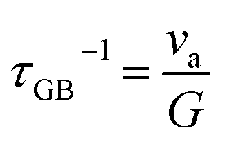
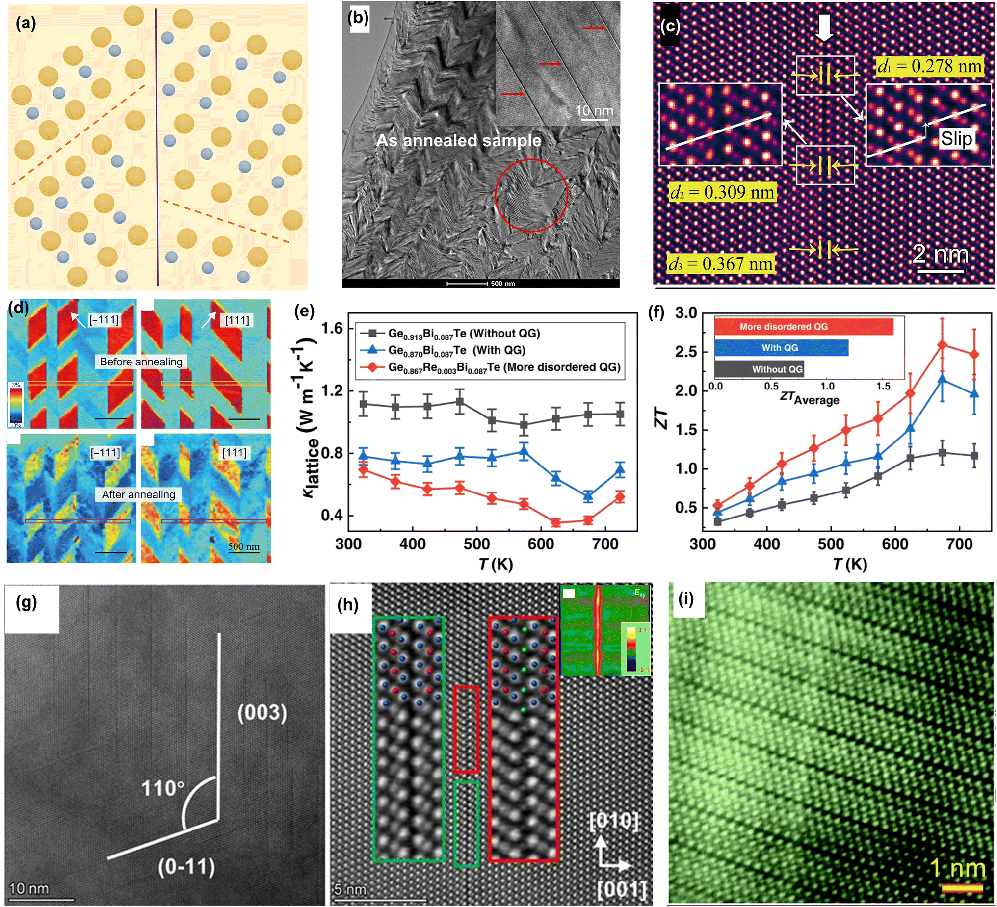
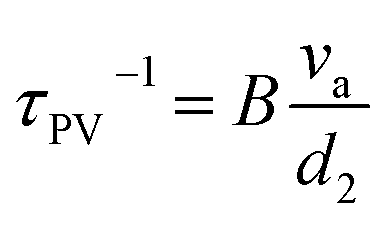
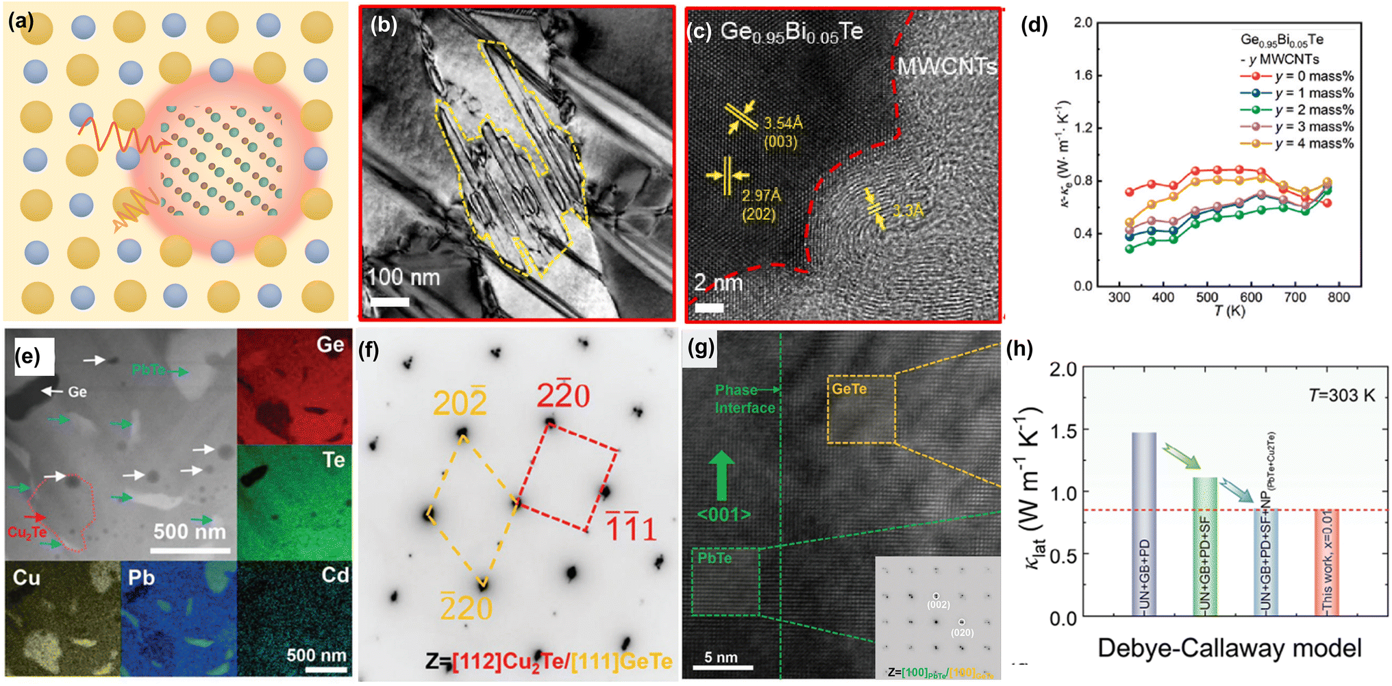
Two-dimensional defects primarily enhance the scattering of low-frequency and mid-frequency phonons. The grain boundary is a typical 2D lattice defect in crystal structures. A reduced grain size, which also suggests the increased grain boundary density, can improve the mechanical strength according to the Hall–Petch relationship and enhance the low-frequency phonon scattering. The relaxation time is shown as follows:| |  | (30) |
where G is the average grain size. The decreased grain size led to the reduction of relaxation time. In GeTe, the reduction of grain size usually relies on restricting grain boundary migration. For example, Bai et al.33 found that the addition of boron inhibited the grain growth due to the Zener pinning effect. Besides the grain boundary, there are a variety of 2D defects in GeTe, playing an important role in scattering phonons.
Domain walls in ferroelectric materials are considered a promising avenue for modulating electrical, optical, magnetic, optical and thermal properties.175–177 These domain walls are the interfaces among different polarization orientation regions for ferroelectric materials. The structural and polarization discontinuity at domain walls lead to anomalous behavior distinct from that observed in single-domain states. Due to crystal lattice distortion present at these domain walls, the phonons can be scattered and the thermal resistance is generated. Inspired by this idea, a high thermal conductivity switching ratio was obtained in PMN-xPT,178 manifesting the role of domain walls in scattering phonons. Given the characteristics of GeTe as a ferroelectric phase at room temperature, 71° and 109° domain structures are most commonly observed in this material (Fig. 18a). This arises from interactions between strain and electrostatic field forces during the transition process from the high-temperature cubic phase to the room-temperature rhombohedral phase—specifically induced by Peierls-distorted bonds. Wu et al.26 investigated the effects of domain structures along with the van der Waals gap (planar vacancy) on the sample performance by intentionally introducing abundant Ge vacancies into the GeTe lattice followed by proper heat treatment. It was revealed that the lattice thermal conductivity reduced from 1.05 W m−1 K−1 to 0.78 W m−1 K−1 and the ZT value increased from 2.0 to 2.4 after heat treatment.
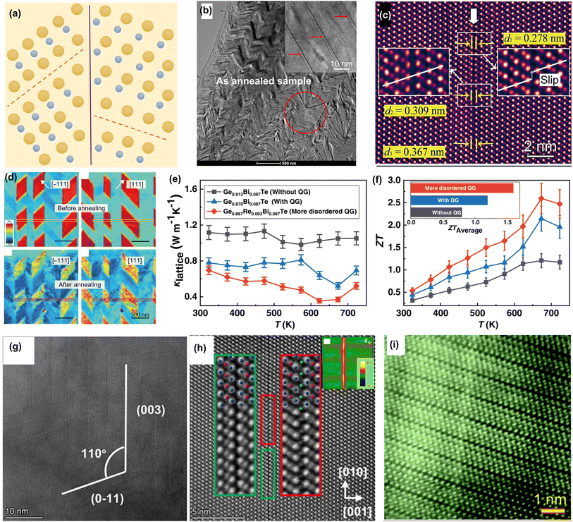 |
| | Fig. 18 (a) Schematic image of the domain structure and planar vacancy. (b) The sample annealed at 300 °C for 2 hours and then cooled down to room temperature. The inserted image shows the high-magnification image of the vdW gaps (planar vacancies). (c) A HRSTEM HAADF image obtained along the [110]PC. (d) The strain field in the [−111] and [111] directions before or after annealing.179 The temperature-dependent (e) lattice thermal conductivity and (f) ZT values.53 (g) TEM image of Ge9Sb2Te11.91 revealing the dense planar vacancies. (h) HRTEM image of one typical planar vacancy with the inset showing the enlarged views of the framed areas and the inset image showing the strain map of a planar vacancy measured by GPA. Reproduced with permission.180 (i) HAADF-STEM image showing the atomic configuration in Ge0.89Cr0.03Sb0.08Te. Reproduced with permission.128 | |
To uncover the underlying mechanism, they used in situ transmission electron microscopy to examine the van der Waals gap.179 Morphologically, a complex hierarchical microdomain–nanodomain-gap structure was observed as shown in Fig. 18b. These negatively charged nanoscale domain walls balance the electric field with the positively charged Ge van der Waals gap within this complex hierarchical structure, resulting in strong scattering effects on mid- and low-frequency phonons. The relaxation time is shown as follows:
| |  | (31) |
and
| |  | (32) |
where prefactors
A and
B are fitting parameters containing the information of scattering efficacy of different planar boundaries and their surrounding strain cores and
d1 and
d2 are the inter-distance between two neighboring domain boundaries and van der Waals gaps, respectively. As shown in
Fig. 18c, the Te–Te distance of 0.278 nm is much shorter in the van der Waals gap area, in contrast to the value of 0.367 nm in the perfect crystal area. The van der Waals gaps in GeTe are an ordering of Ge vacancies, terminated at two edge dislocations, beyond which the GeTe lattice recovers into an intact state. The authors predicted that the van der Waals gaps were induced by a strain field perpendicular to them during the martensitic phase transition in the cooling process according to the
in situ observation and strain analysis in domains (
Fig. 18d). They treated the van der Waals gap as a stacking fault within an edge dislocation loop. The growth of the planar vacancies is similar to the positive climbing of edge dislocation. The climbing of the planar vacancies is driven by mechanical force (strain field) and chemical force (vacancy concentration), where the mechanical force turns out to be dominant according to the theoretical calculation results. In the nucleation of planar vacancies, enough mechanical force is required to overcome the nucleation resistance. Usually, the formation of high-concentration van der Waals gaps induces the generation of hierarchical domain structures, suppressing the lattice thermal conductivity together. However, the domain structure disappeared after the phase transition at elevated temperatures. Therefore, the work focused on van der Waals gaps (planar vacancies) was carried out.
In a recent study by Yu et al.,53 they treated van der Waals gaps as quantum gaps due to the small gap between Te atoms and extensively investigated their impact on thermoelectric performance. They compared two series of samples, with or without quantum gaps. Samples with higher defect concentrations exhibited higher phonon scattering rates, which increase the Grüneisen constant and lower the phonon average velocities, thereby decreasing the lattice thermal conductivity (Fig. 18e). Due to the negligible effect on electrical properties, the ZT value was boosted to 2.6 as shown in Fig. 18f. In addition, in Ge9Sb2Te11.91, high concentrations of planar vacancies embedded in the matrix were discovered, which are parallel to either (003) or (0![[1 with combining macron]](https://www.rsc.org/images/entities/char_0031_0304.gif) 1) directions.180 The HRTEM shows a missing layer of Ge atoms between two adjacent Te atomic planes with a lattice spacing, as shown in Fig. 18g. Ge planar vacancies generate large strains in the lattice (Fig. 18h). The strategy to introduce planar vacancies above is to alloy Bi2Te3 or Sb2Te3 according to eqn (15). The formation of planar vacancies can also be induced by doping elements. Cd/Bi co-doping also favors the formation of planar vacancies, which is attributed to the reduced formation energy of planar vacancies.22 In addition, observations from (Cr, Sb) doped GeTe samples revealed a seven-atomic-layered lattice.128 The formation of this type of structure can be ascribed to the layer-structured GeSb2Te4 (Fig. 18i). The authors suggested that Cr doping could lower the formation energy of GeSb2Te4, which is the energetic reason for the formation of a layered structure. In conclusion, the formation of the planar vacancies or van der Waals gaps is connected to the strain field, the vacancy concentration and the dopants.
1) directions.180 The HRTEM shows a missing layer of Ge atoms between two adjacent Te atomic planes with a lattice spacing, as shown in Fig. 18g. Ge planar vacancies generate large strains in the lattice (Fig. 18h). The strategy to introduce planar vacancies above is to alloy Bi2Te3 or Sb2Te3 according to eqn (15). The formation of planar vacancies can also be induced by doping elements. Cd/Bi co-doping also favors the formation of planar vacancies, which is attributed to the reduced formation energy of planar vacancies.22 In addition, observations from (Cr, Sb) doped GeTe samples revealed a seven-atomic-layered lattice.128 The formation of this type of structure can be ascribed to the layer-structured GeSb2Te4 (Fig. 18i). The authors suggested that Cr doping could lower the formation energy of GeSb2Te4, which is the energetic reason for the formation of a layered structure. In conclusion, the formation of the planar vacancies or van der Waals gaps is connected to the strain field, the vacancy concentration and the dopants.
4.4. 3D defects
According to the calculation of the mean free path of phonons for GeTe, the introduction of nanoinclusions with a size of 10–100 nm can enhance the phonon scattering (Fig. 19a). The phonon scattering relaxation time for the nanoinclusions can be expressed as follows:181| |  | (33) |
where R is the average radius for the precipitates, D is the matrix density, ΔD is the density difference between the precipitate and matrix, and Np is the number density of precipitates, respectively. Si et al.182 successfully reduced the lattice thermal conductivity by adding multi-walled carbon nanotubes (MWCNTs). The TEM bright field image showed the structure of the matrix and MWCNTs as shown in Fig. 19b. The morphology of the MWCNTs showed a diameter of ∼30 nm and the length ranges from hundreds of nanometers to microns in the matrix (Fig. 19c). The total thermal conductivity drops from ∼2.3 W m−1 K−1 for Ge0.95Bi0.05Te to ∼1.8 W m−1 K−1 for Ge0.95Bi0.05Te – 2 mass% MWCNTs at 323 K. Due to the negligible effect on carrier transport, the electronic thermal conductivity was hardly changed after incorporating MWCNTs. As a result, the lattice thermal conductivity decreased from ∼0.7 W m−1 K−1 for Ge0.95Bi0.05Te to ∼0.3 W m−1 K−1 for Ge0.95Bi0.05Te – 2 mass% MWCNTs at 323 K as shown in Fig. 19d. Zhu et al.50 discovered that by incorporating Cu2Te into Ge0.84Cd0.06Pb0.10Te, a coherent nano-network across multiple phases was constructed as shown in Fig. 19e. There were PbTe and Cu2Te nano-precipitates in the GeTe matrix, and the interfaces among them were coherent, which were characterized by selected area electron diffraction and high-resolution transmission microscopy (Fig. 19f and g). Fig. 19h shows the reduced lattice thermal conductivity with the alloying of Cu2Te. The Debye–Callaway model was also carried out to investigate the effect of the scattering sources. The results suggested the important role of nano-precipitates in scattering phonons. The minimum lattice thermal conductivity was reduced to 0.33 W m−1 K−1. Table 3 shows the effect of different nanoinclusions/inclusions on transport properties, indicating that the composite strategy is also a promising method for optimizing thermoelectric performance of GeTe.
 |
| | Fig. 19 (a) Schematic view of precipitates in the matrix. (b) The TEM image of the GeTe matrix incorporating multi-walled carbon nanotubes. (c) The HRTEM image showing the structure of GeTe and multi-walled carbon nanotubes. (d) The temperature-dependent lattice thermal conductivity for Ge0.95Bi0.05Te – y mass% MWCNTs. (e) The STEM and corresponding EDS images. (f) The diffraction spots of the Cu2Te phase along the [112] direction and the overlapped diffraction pattern of the GeTe phase along the [111] direction, marked in yellow. (g) HRTEM image of an interface between PbTe and GeTe; the inset image shows diffraction spots of the GeTe phase and the PbTe phase both along the [100] direction. (h) The calculated lattice thermal conductivity using the Debye–Callaway model at 303 K. | |
Table 3 The thermoelectric properties at room temperature by incorporating different nanoinclusions/inclusions (units: κ, κL: W m−1 K−1, σ: 103 S cm−1, and S: μV K−1)
| Samples |
κ
|
κ
L
|
σ
|
S
|
ZT
max
|
| MWCNTs/Ge0.95Bi0.05Te182 |
0.2 wt% |
∼1.8 |
∼0.3 |
∼2.8 |
∼87 |
∼2.3 |
| × |
∼2.3 |
∼0.7 |
∼2.8 |
∼87 |
∼2.0 |
| Cu2Te/Ge0.84Cd0.06Pb0.10Te50 |
0.1 mol |
∼1.24 |
∼0.86 |
∼0.74 |
∼154 |
∼2.22 |
| × |
∼2.37 |
∼0.9 |
∼2.36 |
∼73 |
∼1.9 |
| Ga/Ge0.9Sb0.1Te46 |
1 at% |
∼1.53 |
∼1.14 |
∼0.75 |
∼146 |
1.97 |
| × |
∼1.60 |
∼1.21 |
∼0.70 |
∼130 |
∼1.74 |
| FeGe2/Ge0.875Sb0.08Te183 |
1.5% |
∼1.83 |
∼0.9 |
∼1.65 |
∼106 |
∼2.1 |
| × |
∼2.42 |
∼1.42 |
∼1.71 |
∼92 |
∼1.8 |
| Fe/Ge0.96Bi0.06Te184 |
2 mol% |
∼2.71 |
∼1.46 |
∼1.99 |
∼74 |
1.68 |
| × |
3.09 |
∼1.62 |
∼2.33 |
∼71 |
1.53 |
| Ge0.84Pb0.1Sb0.06TeB0.07 (ref. 33) |
7 mol% |
— |
— |
— |
— |
2.2 |
| FeTe2/Ge0.9Sb0.1Te185 |
1.0% |
∼1.45 |
∼1.04 |
∼0.83 |
∼143 |
2.1 |
| B/Ge0.94Bi0.05Te47 |
0.1 wt% |
2.47 |
0.73 |
2.99 |
92.16 |
2.45 |
| Ge0.78Ga0.01Pb0.1Sb0.07Te46 |
— |
∼1.3 |
0.8 |
∼1.15 |
∼120 |
2.1 |
5. Progress in thermoelectric devices and modules
Recently, a high ZT value of over 2.0 has been already achieved in GeTe-based thermoelectric materials through the implementation of diverse strategies, showing great potential in fabrication of thermoelectric devices. However, besides the superior thermoelectric performance of p-type and n-type materials, the high efficiency of thermoelectric devices relies on the geometry optimization and the module assembly as shown in Fig. 20.186 While integrating p-type legs with n-type legs, the cross-sectional area ratio and width are also key geometric parameters. Furthermore, the design of diffusion barrier layers should be carefully considered; ideal barrier layers are expected to be chemically inert but mechanically adhesive, and their work function and thermal expansion coefficient should match with those of the TE legs, so as to achieve low thermal and electrical resistivities at the interface. High mechanical and thermal stabilities at high temperatures are also required for diffusion barrier layers. In essence, critical factors also encompassing mechanical strength and thermal strain induced by the phase transition need to be taken into account.71,111
 |
| | Fig. 20 Logical framework for the full-parameter optimization of a thermoelectric power generation module.186 | |
5.1 Simulation and measurement
To achieve maximum efficiency, geometry optimization is essential. The Seebeck coefficient, electrical conductivity and thermal conductivity are all temperature-dependent; the geometry of devices and modules affect the temperature distribution, heat flow, etc. In segmented single-leg devices, maximizing the single-leg device efficiency necessitates geometry optimization to determine the optimal proportions of working materials and establish their ideal height ratio. Thus, each part of a thermoelectric material can work in an appropriate temperature range. Furthermore, as for modules with p- and n-type thermoelectric legs, simulating cross-sectional areas of p- and n-legs is crucial for maximizing output power density and conversion efficiency. Fig. 21a and d show the schematic view of one segmented single-leg device and module, respectively.187,188Fig. 21b and c illustrate the contour map of output power density and conversion efficiency as a function of the height ratio and current for the segmented single-leg device. At x = 0.77 and I = 9.22 A, the maximum output power density is 16.4 mW mm−2 when Th = 723 K, while the simulated ηmax reaches 15.9% when x = 0.66 and I = 7.05 A. The conversion efficiency reached 9.5% for the segmented GeTe/(Bi,Sb)2Te3 thermoelectric leg.187Fig. 21e and f show the simulated output power density and conversion efficiency as a function of the ratio of the cross-sectional areas of the p- to n-legs (Ap/An) and the ratio of the height to the total cross-sectional area (H/Apn). The simulated conversion efficiency reached 13.7%.188 Here, the n-type leg is skutterudite (SKD), which exhibits high thermoelectric performance at high temperatures and a comparable thermal expansion coefficient to p-type GeTe. As can be seen, increasing H/Apn would benefit the conversion efficiency because a large H ensures an increased ΔT over the thermoelectric leg. By contrast, output power density decreases with increasing H/Apn, attributed to the large H of thermoelectric legs, leading to high internal resistance. The as-fabricated modules exhibited a high conversion efficiency of 12% as illustrated in Fig. 21h. Jiang et al.38 conducted preparation and testing on modules with varying length ratios using p-type GeTe and n-type PbTe with the low temperature part of Bi2Te3-based thermoelectric materials. The module labeled as 11 consisted of uniform legs of Ge0.61Ag0.11Sb0.13Pb0.12Bi0.01Te and Pb0.997In0.003Te0.996I0.004 thermoelectric materials. The ratios (7![[thin space (1/6-em)]](https://www.rsc.org/images/entities/char_2009.gif) :3, 8:3 and 9:3) in Fig. 21i are the length ratios of the segmented legs, coupled with p-type Bi0.5Sb1.5Te3 and n-type Bi2Te2.7Se0.3, respectively. It shows the efficiencies of different modules at 500 K and 800 K, respectively, in which the highest efficiency is 13.3% for a length ratio of 8:3. These studies illustrate the importance of geometry optimizations in the fabrication of devices or modules. However, there are still differences between the simulated and measured results. It is significant to select proper diffusion layer materials for pursuing devices or modules with high conversion efficiency.
:3, 8:3 and 9:3) in Fig. 21i are the length ratios of the segmented legs, coupled with p-type Bi0.5Sb1.5Te3 and n-type Bi2Te2.7Se0.3, respectively. It shows the efficiencies of different modules at 500 K and 800 K, respectively, in which the highest efficiency is 13.3% for a length ratio of 8:3. These studies illustrate the importance of geometry optimizations in the fabrication of devices or modules. However, there are still differences between the simulated and measured results. It is significant to select proper diffusion layer materials for pursuing devices or modules with high conversion efficiency.
 |
| | Fig. 21 (a) Schematic diagram of a segmented GeTe/(Bi,Sb)2Te3 thermoelectric leg. (b and c) Contour map of power density (Pd) and efficiency (η) when Th = 723 K and Tc = 303 K.187 (d) Schematic illustration of p-GeTe and n-SKD modules. Simulated (e) Pd and (f) ηmax for the GeTe/SKD module when Th = 873 K and Tc = 293 K.188 (g) η–I relationship of GeTe/(Bi,Sb)2Te3 segmented one-leg TE modules. (h) η of the module as a function of the current I at different operating temperatures. (i) Conversion efficiencies for the fabricated 11, 7:3, 8:3, and 9:3 modules.38 | |
5.2 Screening the diffusion barrier materials
Fig. 22 indicates some selected standards taking metals as examples. Xing et al.189 conducted a comprehensive study on the interfaces between GeTe and 12 different metals (Cr, Hf, Nb, Ti, Mo, Ni, Ta, Zr, Al, Co, V, and Fe), respectively, by mixing them with GeTe powders followed by the SPS technique. Based on the morphological analysis of various interfaces (Fig. 22a), these materials can be categorized into three types. The first type of interface includes Nb/GeTe and Ta/GeTe, which display large gaps at the interfaces, indicating poor contact that may increase the resistance and degrade the mechanical strength. The second type comprises Fe/GeTe and Ni/GeTe interfaces, which form Fe–Te and Ni–Te binary compounds, respectively, suggesting a too rapid reaction rate with the GeTe matrix. The third category consists of materials capable of establishing reaction layers at the interfaces and good contact with the GeTe matrix. The authors measured the thickness of these reaction layers as illustrated in Fig. 22b, where the interfacial reaction between Mo and the matrix gave rise to a thin reaction layer with a thickness of less than 1 μm. Furthermore, it is crucial to consider the work function difference as it can influence interface contact resistance within devices. For n-type materials, the work function of the diffusion barrier materials should be lower than that of thermoelectric materials; conversely, for p-type materials, it should be higher than that of thermoelectric materials. As depicted in Fig. 22c, Pei et al.187 reported data about work functions for GeTe materials alongside various diffusion barrier materials. Subsequent analysis using SEM and energy dispersive spectroscopy (EDS) revealed that the thickness of the Ti diffusion layer is 3 μm. Therefore, Ti was selected as an interconnection layer between copper electrodes and GeTe.
 |
| | Fig. 22 (a) Microstructures of typical interfaces between GeTe and 12 kinds of pure metals (Cr, Hf, Nb, Ti, Mo, Ni, Ta, Zr, Al, Co, V, and Fe). The central image shows the schematic map of the sample integrating different interfaces.189 (b) Thickness of reaction layers between GeTe and different pure metals. (c) Work function and linear expansivity of GeTe and some metals as metallization layers. | |
Another critical factor is the thermal expansion coefficient. The thermal expansion coefficients of rhombohedral GeTe (11.2 × 10⁻⁶ K−1) and cubic GeTe (23.4 × 10⁻⁶ K−1) differ significantly.111 Consequently, under a temperature gradient, this disparity in thermal expansion coefficients induces volume change and substantial thermal stress within the GeTe device, potentially leading to crack formation at the interface and adversely affecting its mechanical properties and stability. To mitigate this issue, two primary strategies can be employed. The first is to lower the phase transition temperature to approximately room temperature through methods such as doping and high-entropy alloying. The second strategy aims to increase the thermal expansion coefficient of rhombohedral GeTe to match that of cubic GeTe. Furthermore, it is essential to select a diffusion barrier material with a thermal expansion coefficient comparable to that of the GeTe material. Pei et al.187 summarized data about linear thermal expansion for GeTe materials and various metals, providing a screening for selection of proper diffusion barrier materials (Fig. 22c). Li et al.33 found that there is a good match between the thermal expansion coefficients of Ge0.9Sb0.1TeB0.01 and Al66Si34 alloys over a wide temperature range. While Al possesses a high thermal expansion coefficient, Si exhibits a lower one; thus, an Al66Si34 alloy was chosen as the diffusion barrier material whose thermal expansion coefficient may be comparable to that of GeTe. A diffusion layer with 10 μm thickness exists between Al66Si34 alloy and GeTe, accompanied by a contact resistance of ∼20.7 μΩ cm2.
As shown in Fig. 23, some materials that can serve as excellent diffusion barrier layers are summarized. Bu et al.34 used SnTe as the diffusion barrier material and Ag as the electrode, achieving a remarkably low contact resistance of ∼8 μΩ cm2 and attaining an efficiency of 14% for single-leg devices. Fig. 23a shows the single-leg device prepared from (Ge0.98Cu0.04Te)0.88(PbSe)0.12. The interfaces between Ag–SnTe and SnTe–GeTe were characterized by SEM (Fig. 23b), where no cracks were observed. The total electrical contact resistance was 0.2 μΩ with a low interfacial contact resistivity of only ∼8 μΩ cm2. Xing et al.189 reported Mo as the diffusion barrier material generating an impressively low contact resistance of less than 1 μΩ cm2 (Fig. 23c). SEM and EDS analyses revealed excellent interfacial integrity along with minimal diffusion layers present in these configurations as shown in Fig. 23d. The contact resistance measurement indicates an extremely low value of <1 μΩ cm2 (Fig. 23e). Additionally, Xie et al.'s investigation188 identified NiGe from the calculated ternary phase diagrams at 0 K based on thermodynamic conditions and the calculated interfacial reaction energy capable of forming chemically inert interfaces with GeTe; notably, the NiGe compound also exhibits enhanced electrical conductivity and thermal conductivity. The solid circles in Fig. 23f indicate the stable phases at 0 K, while the empty circle represent the unstable phases. As shown in Fig. 23f, the positive interfacial interaction energy for NiGe indicates that it is chemically inert to GeTe, rendering it a potential diffusion barrier material. HRTEM was used to characterize the GeTe/NiGe interface. The EDS mapping shows a good interface according to the element distributions as illustrated in Fig. 23g and h. As a result, a low interfacial contact resistivity at the GeTe/NiGe interface of ∼1 μΩ cm2 was acquired and remained below 3 μΩ cm2 after aging at 773 K for 10 days. The subsequent Fig. 23i and j illustrate several commonly employed diffusion barrier layers in GeTe-based devices along with their respective contact resistances.
 |
| | Fig. 23 (a) Experimental setup for the device efficiency measurement. (b) EDS mapping of the contacts. (c) Room-temperature contact resistance using a line scanning technique.34 (d) SEM image and EDS elemental mapping performed near the interfaces of the GeTe/Mo/GeTe sandwich leg. (e) Resistance (R) line scanning across the interfaces for the electrical contact resistivity measurement.189 (f) Calculated phase equilibria diagrams (PEDs) at 0 K for the Ni–Ge–Te system. Solid and empty circles represent stable and unstable phases at 0 K. Calculated interfacial reaction energy (EIR) between GeTe and the diffusion barrier material for the Ni–Ge–Te system. (g) Energy-dispersive spectrometry (EDS) mapping. (h) Atomic structure to show a sharp interface between GeTe and NiGe.188 (i) The interfacial contact resistivity in GeTe devices.190. (j) Interfacial contact resistivity of NiGe, FeGe2, Mo, Ti, Al66Si34, and SnTe barrier layers after aging. “Broken” in (j) means that the Fe layer peels off the GeTe matrix and the GeTe/Fe interface is broken after the aging.188 | |
In addition to the properties of diffusion barrier materials, reliable mechanical properties are also crucial for the fabrication of devices and modules. Favorable mechanical properties enhance the potential for subsequent mechanical processing of the sample. The mechanical properties of pristine GeTe can be enhanced through doping or composite approaches. The point defects can reinforce the mechanical strength through doping. The medium-entropy alloyed GeTe samples showed a Vickers hardness of 270 Hv for Ge0.63Mn0.15Pb0.1Sb0.06Cd0.06Te compared to 134 Hv for the pristine sample.36 In addition, the phase transition temperature was reduced to near room temperature. On the other hand, Zhang et al.33 successfully improved both the compressive strength and Vickers hardness of the material via boron incorporation while simultaneously reducing the thermal expansion coefficient disparity before and after the phase transition as illustrated in Fig. 24a–c. Zhu et al.50 also introduced composites of Cu2Te and PbTe into the GeTe matrix through Cu2Te alloying combined with Pb and Cd doping, resulting in a notable enhancement in Vickers hardness and significant improvement in compressive strain (Fig. 24d and e). Fig. 24d illustrates the comparison of Vickers hardness for GeTe-based materials. Additionally, interface bonding strength is an important factor, which relies on the reaction layers between GeTe and diffusion barrier materials. If the reaction layer is thinner, the thermal resistance and electrical resistance of the device will be reduced, but the interface strength may not be sufficient for module fabrication, leading to module failure.191Fig. 24f summarizes the shear strength for GeTe-based materials observed for various material interfaces, which provides potential diffusion barrier materials for device fabrication. Tables 4 and 5 illustrate the relevant information about the single devices or modules, respectively, indicating the high performance of GeTe devices and modules.
 |
| | Fig. 24 (a) Compressive strength and (b) Vickers hardness of Ge0.9Sb0.1TeBx. (c) Temperature dependence of relative length variation (dL/L0).33 (d) Comparison of room-temperature Vickers microhardness Hv. (e) Comparison of compressive tests of GeTe and some other typical brittle thermoelectric materials.50 (f) Comparison of the shear strength of the segmented legs and some joints.190 | |
Table 4 Performance of single-leg GeTe-based devices
| Materials |
Barrier/electrode |
P
max (W) |
η
max (%) |
ΔT (K) |
| Ge0.93Bi0.06In0.01Te27 |
Fe/Ag |
0.55 |
12.3 |
445 |
| (Pb0.15Ge0.85Te)0.8(AgSbTe2)0.2 (ref. 42) |
SnTe/Fe |
0.165 |
14.8 |
500 |
| 0.9GeTe–0.03CuBiSe2–0.07PbTe192 |
SnTe/InGa |
0.08 |
13.4 |
500 |
| Bi0.07Ge0.90Te39 |
Mo/InGa |
0.14 |
11.0 |
498 |
| Bi0.05Ge0.99Te/(Bi,Sb)2Te3 (ref. 187) |
GeTe/Ti/Cu, (Bi,Sb)2Te3/Ni/Cu |
— |
9.5 |
423 |
| Ge0.87Y0.02Sb0.10Ag0.01Te43 |
SnTe/Fe |
0.2 |
13.4 |
463 |
| B-Bi0.05Ge0.94Te/Bi0.4Sb1.6Te3.01 (ref. 47) |
GeTe/Ti/Cu, (Bi,Sb)2Te3/Ni/Cu |
0.186 |
13.7 |
456 |
| Ge0.76Pb0.10Bi0.06Sb0.04Te/(Bi0.4Sb1.6Te3)0.97(MgB2)0.03 (ref. 190) |
— |
∼0.095 |
15.5 |
450 |
| Ge0.9Sb0.1Te/Bi0.5Sb1.5Te3 (ref. 193) |
Ag/GeTe/(Bi,Sb)2Te3/Ni |
∼0.077 |
13.6 |
493 |
| (Ge0.98Cu0.04Te)0.88(PbSe)0.12 (ref. 34) |
SnTe/Ag |
∼0.13 |
∼14 |
440 |
| Ge0.93Ti0.01Bi0.06Te–0.01Cu134 |
Mo/Ni |
∼0.04 |
10.5 |
423 |
| Ge0.94Bi0.06Te/Bi0.5Sb1.5Te3 |
— |
— |
10.3 |
419 |
Table 5 Performance of GeTe-based modules
| p-Type materials |
n-Type materials |
Pairs |
P
max (W) |
η
max (%) |
ΔT (K) |
| Ge0.92Sb0.04Bi0.04Te0.95Se0.05 (ref. 189) |
Yb0.3Co4Sb12 |
8 |
2 |
7.8 |
500 |
| Ge0.84Pb0.1Sb0.06TeB0.07 (ref. 33) |
Yb0.3Co4Sb12 |
4 |
1.3 |
5.64 |
425 |
| Ge0.84Pb0.1Sb0.06TeB0.07 (ref. 33) |
Yb0.3Co4Sb12 |
9 |
9.2 |
7.4 |
477 |
| Ge0.92Bi0.08Te0.92I0.08 (ref. 194) |
Yb0.075CoSb3 |
8 |
1.2 |
12 |
500 |
| (Ge0.84Cd0.06Pb0.10Te)0.99(Cu2Te)0.01 (ref. 50) |
Yb0.3Co4Sb12 |
7 |
0.4 |
7 |
400 |
| Ge0.89Cu0.06Sb0.08Te188 |
Yb0.3Co4Sb12 |
8 |
4.0 |
12 |
545 |
| Ge0.78Ga0.01Pb0.1Sb0.07Te46 |
Yb0.3Co4Sb12 |
18 |
7.86 |
5.85 |
476 |
| (Pb0.15Ge0.85Te)0.8(AgSbTe2)0.2 (ref. 42) |
Mg3.15Co0.05Sb1.24Bi0.75Se0.01 |
— |
0.78 |
14.5 |
480 |
| Ge0.83Mn0.09Ti0.02Bi0.06Te195 |
Multi-segmented Mg3(Sb, Bi)2 |
1 |
0.38 |
12.8 |
480 |
| (Ge0.84Sb0.06Pb0.1Te)0.99(AgCuTe)0.01 (ref. 160) |
PbTe-based material |
17 |
1.93 |
7.9 |
500 |
| Ge0.61Ag0.11Sb0.13Pb0.12Bi0.01Te38 |
Pb0.997In0.003Te0.996I0.004 |
— |
3.5 |
13.3 |
500 |
6. Summary and outlook
In summary, great advancements and developments have been achieved in GeTe thermoelectric materials. We have delineated the intrinsic characteristics of GeTe materials, encompassing the bonding structure, band structure, phonon structure, and defect structure. Additionally, we have summarized contemporary methods for performance optimization. The bonding structure offers fundamental insights into the unique properties of GeTe, while its distinctive phase transition structure introduces new degrees of freedom for performance enhancement. By investigating the band and defect structures, we can effectively optimize the electrical and phonon transport properties of these materials. As for electrical transport properties, the power factor can be improved by band engineering, carrier density optimization, energy filtering and rational processes. Furthermore, the analysis of weighted mobility enables us to observe variations in electrical transport performance from another insight to select dopants. As for phonon transport properties, the phonon structure provides useful guidance for optimizing lattice thermal conductivity. Through the introduction of 0D, 1D, 2D and 3D defects, phonons with different frequencies can be scattered effectively.
Moreover, through quality factor analysis, we can evaluate how dopants affect the thermoelectric potential of the material, providing valuable insights into ZT enhancement as shown in Fig. 25. According to simulations, the quality factors of GeTe can be 0.3 and 1.5 at 300 K and 700 K, respectively; based on current data levels, there remains significant room for improvement. The quality factor is determined by the weighted mobility and lattice thermal conductivity, reflecting the microscopic transport characteristics of electrons and phonons, respectively. Research into multi-element co-doping as well as medium-entropy and high-entropy materials has emerged as a prominent trend that significantly reduces the carrier concentration while enhancing the Seebeck coefficient and suppressing lattice thermal conductivity, increasing the ZT value profoundly; however, this often leads to significant loss in carrier mobility, deteriorating the weighted mobility. Therefore, to achieve further enhancements in performance, it is essential to implement multiple strategies that consider mobility.
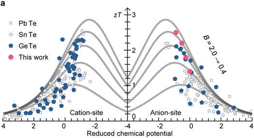 |
| | Fig. 25 Comparison of the quality factor (B) and figure-of-merit (ZT) of GeTe, PbTe, and SnTe thermoelectric materials with cationic and anionic doping.194 | |
A rational fabrication process and composite incorporation are robust strategies for enhancing their properties. Optimizing the performance of GeTe materials through rational process design can effectively optimize the structure of Ge vacancies, serving as a strategic approach to improve carrier mobility. Furthermore, a rational process and the introduction of specific dopants are pivotal in constructing hierarchical domain structures that significantly scatter phonons while exerting minimal influence on carrier transport. The judicious selection of composites can also concurrently enhance both electrical and thermal transport properties, potentially establishing a trend in future research on GeTe-based thermoelectric materials. Additionally, the development of specialized microstructures within GeTe warrants careful consideration; for instance, modifying grain boundaries or introducing nanopores may substantially improve performance of GeTe-based thermoelectric materials.
In terms of synthesis technology, beyond traditional methods such as hot pressing and spark plasma sintering (SPS), it is essential to explore innovative synthesis techniques. For example, employing 3D printing additive manufacturing could markedly expedite the production of bulk GeTe samples. Moreover, utilizing the Bridgman method for fabricating single crystal GeTe is crucial for achieving deeper insights into the structure–performance relationship inherent in these samples.
In the field of devices, research on high-performance devices and modules has advanced considerably. For the diffusion barrier layers in GeTe-based thermoelectric devices, it is imperative to attain low resistance, superior mechanical properties and thermal stability, and compatible thermal expansion coefficients while accommodating a reaction layer with a proper thickness (low contact resistance (both electrical and thermal) but high bonding strength). Specifically, metals employed as diffusion barrier layers have been thoroughly investigated. In contrast, studies concerning compounds as diffusion barrier layers remain relatively sparse.
Although significant progress has been made in understanding contact resistance, investigations on the compatibility of mechanical properties and thermal expansion coefficients at the interfaces are still insufficiently developed, especially under the externally applied mechanical or thermal stresses upon thermal cycling. These parameters are related to the reliability of the thermoelectric modules in real applications, such as deep space probes. Mechanical properties encompass both the intrinsic characteristics of the material and the bonding strength at the interface. Given that GeTe exhibits a high density of vacancies, its mechanical performance may be adversely affected, potentially leading to material failure at elevated temperatures. Enhancing both the mechanical properties of GeTe and its interfacial bonding strength is vital for advancing micro-scale GeTe thermoelectric materials and devices in future applications. The thermal expansion coefficient should account for variations within GeTe itself as well as its compatibility with adjacent barrier layers and electrodes. Additionally, attention must be directed towards matching thermal expansion coefficients between p-type and n-type GeTe materials; the way achieving n-type GeTe-based thermoelectric materials with performance comparable to their p-type counterparts is critically important. More studies on device stability and longevity are encouraged, and thus performance evaluation for samples subjected to prolonged annealing is necessary for further applications.
Data availability
All the data that support this study are included in this article.
Author contributions
All authors contributed to the conceptualization and writing of the article. Y. J. drafted the initial manuscript. C. Y., H.-L. Z., and H. L. provided input and revisions, and J.-F. L. performed the final editing.
Conflicts of interest
There are no conflicts to declare.
Acknowledgements
This work was supported by the National Key R&D Program of China (2023YFB3809400), the Basic Science Center Project of the National Natural Science Foundation of China (52388201), and the China Postdoctoral Science Foundation (2023M731870). J. Y. acknowledge financial support from the Shuimu Tsinghua Scholar Program (2023SM098). H. L. acknowledge financial support from the Shuimu Tsinghua Scholar Program (2022SM045). H.-L. Z. acknowledge financial support from the Shuimu Tsinghua Scholar Program (2022SM119).
References
- J.-F. Li, W.-S. Liu, L.-D. Zhao and M. Zhou, NPG Asia Mater., 2010, 2, 152 CrossRef.
- J. Mao, Z. Liu, J. Zhou, H. Zhu, Q. Zhang, G. Chen and Z. Ren, Adv. Phys., 2018, 67, 69 CrossRef.
- G. J. Snyder and E. S. Toberer, Nat. Mater., 2008, 7, 105 CrossRef PubMed.
- F. D. Rosi, J. P. Dismukes and E. F. Hockings, Electr. Eng., 1960, 79, 450 Search PubMed.
- D. A. Wright, Metall. Rev., 1970, 15, 147 CrossRef.
- S. K. Plachkova, Phys. Status Solidi A, 1984, 83, 349 CrossRef.
- G. C. Christakudis, S. K. Plachkova, L. E. Shelimova and E. S. Avilov, Phys. Status Solidi A, 1991, 128, 465 CrossRef.
- S. H. Yang, T. J. Zhu, T. Sun, J. He, S. N. Zhang and X. B. Zhao, Nanotechnology, 2008, 19, 245707 CrossRef PubMed.
- E. M. Levin, B. A. Cook, J. L. Harringa, S. L. Bud’ko, R. Venkatasubramanian and K. Schmidt-Rohr, Adv. Funct. Mater., 2011, 21, 441 CrossRef.
- E. M. Levin, S. L. Bud’ko and K. Schmidt-Rohr, Adv. Funct. Mater., 2012, 22, 2766 CrossRef.
- Y. Gelbstein, J. Davidow, S. N. Girard, D. Y. Chung and M. Kanatzidis, Adv. Energy Mater., 2013, 3, 815 CrossRef CAS.
- D. Wu, L.-D. Zhao, S. Hao, Q. Jiang, F. Zheng, J. W. Doak, H. Wu, H. Chi, Y. Gelbstein, C. Uher, C. Wolverton, M. Kanatzidis and J. He, J. Am. Chem. Soc., 2014, 136, 11412 CrossRef CAS.
- F. Fahrnbauer, D. Souchay, G. Wagner and O. Oeckler, J. Am. Chem. Soc., 2015, 137, 12633 CrossRef CAS.
- T. Schröder, T. Rosenthal, N. Giesbrecht, M. Nentwig, S. Maier, H. Wang, G. J. Snyder and O. Oeckler, Inorg. Chem., 2014, 53, 7722 CrossRef.
- E. Hazan, N. Madar, M. Parag, V. Casian, O. Ben-Yehuda and Y. Gelbstein, Adv. Electron. Mater., 2015, 1, 1500228 CrossRef.
- S. Perumal, P. Bellare, U. S. Shenoy, U. V. Waghmare and K. Biswas, Chem. Mater., 2017, 29, 10426 CrossRef.
- M. Samanta and K. Biswas, J. Am. Chem. Soc., 2017, 139, 9382 Search PubMed.
- J. Li, Z. Chen, X. Zhang, Y. Sun, J. Yang and Y. Pei, NPG Asia Mater., 2017, 9, e353 CrossRef.
- J. Li, X. Zhang, S. Lin, Z. Chen and Y. Pei, Chem. Mater., 2017, 29, 605 CrossRef.
- S. Schwarzmüller, M. Jakob, M. Nentwig, T. Schröder, A. Kuhn, A. Düvel, P. Heitjans and O. Oeckler, Chem. Mater., 2018, 30, 7970 CrossRef.
- J. Li, X. Zhang, X. Wang, Z. Bu, L. Zheng, B. Zhou, F. Xiong, Y. Chen and Y. Pei, J. Am. Chem. Soc., 2018, 140, 16190 CrossRef PubMed.
- M. Hong, Y. Wang, W. Liu, S. Matsumura, H. Wang, J. Zou and Z.-G. Chen, Adv. Energy Mater., 2018, 8, 1801837 CrossRef.
- M. Hong, Z.-G. Chen, L. Yang, Y.-C. Zou, M. S. Dargusch, H. Wang and J. Zou, Adv. Mater., 2018, 30, 1705942 CrossRef PubMed.
- X. Zhang, J. Li, X. Wang, Z. Chen, J. Mao, Y. Chen and Y. Pei, J. Am. Chem. Soc., 2018, 140, 15883 CrossRef PubMed.
- J. Li, X. Zhang, Z. Chen, S. Lin, W. Li, J. Shen, I. T. Witting, A. Faghaninia, Y. Chen, A. Jain, L. Chen, G. J. Snyder and Y. Pei, Joule, 2018, 2, 976 CrossRef.
- D. Wu, L. Xie, X. Xu and J. He, Adv. Funct. Mater., 2019, 29, 1806613 CrossRef.
- S. Perumal, T. Ghosh, A. Singh and K. Biswas, Joule, 2019, 10, 2565 CrossRef.
- J. Dong, F.-H. Sun, H. Tang, J. Pei, H.-L. Zhuang, H.-H. Hu, B.-P. Zhang, Y. Pan and J.-F. Li, Energy Environ. Sci., 2019, 12, 1396 RSC.
- Z. Liu, W. Gao, W. Zhang, N. Sato, Q. Guo and T. Mori, Adv. Energy Mater., 2020, 10, 2002588 CrossRef.
- M. Hong, W. Lyv, M. Li, S. Xu, Q. Sun, J. Zou and Z.-G. Chen, Joule, 2020, 4, 2030 CrossRef.
- X. Xu, Y. Huang, L. Xie, D. Wu, Z. Ge and J. He, Chem. Mater., 2020, 32, 1693 CrossRef.
- T. Xing, C. Zhu, Q. Song, H. Huang, J. Xiao, D. Ren, M. Shi, P. Qiu, X. Shi, F. Xu and L. Chen, Adv. Mater., 2021, 33, 2008773 CrossRef.
- G. Bai, Y. Yu, X. Wu, J. Li, Y. Xie, L. Hu, F. Liu, M. Wuttig, O. Cojocaru-Mirédin and C. Zhang, Adv. Energy Mater., 2021, 11, 2102012 CrossRef.
- Z. Bu, X. Zhang, B. Shan, J. Tang, H. Liu, Z. Chen, S. Lin, W. Li and Y. Pei, Sci. Adv., 2021, 7, eabf2738 CrossRef.
- M. Li, Q. Sun, S.-D. Xu, M. Hong, W.-Y. Lyu, J.-X. Liu, Y. Wang, M. Dargusch, J. Zou and Z.-G. Chen, Adv. Mater., 2021, 33, 2102575 CrossRef.
- S. Zhi, J. Li, L. Hu, J. Li, N. Li, H. Wu, F. Liu, C. Zhang, W. Ao, H. Xie, X. Zhao, S. J. Pennycook and T. Zhu, Adv. Sci., 2021, 8, 2100220 CrossRef.
- D.-Z. Wang, W.-D. Liu, M. Li, L.-C. Yin, H. Gao, Q. Sun, H. Wu, Y. Wang, X.-L. Shi, X. Yang and Q. Liu, Chem. Eng. J., 2022, 441, 136131 CrossRef.
- B. Jiang, W. Wang, S. Liu, Y. Wang, C. Wang, Y. Chen, L. Xie, M. Huang and J. He, Science, 2022, 377, 208 CrossRef.
- Y. Jiang, J. Dong, H.-L. Zhuang, J. Yu, B. Su, H. Li, J. Pei, F.-H. Sun, M. Zhou, H. Hu, J.-W. Li, Z. Han, B.-P. Zhang, T. Mori and J.-F. Li, Nat. Commun., 2022, 13, 6087 CrossRef PubMed.
- S. Duan, W. Xue, H. Yao, X. Wang, C. Wang, S. Li, Z. Zhang, L. Yin, L. Huang, X. Wang, C. Chen, J. Sui, Y. Chen, J. Mao, F. Cao, Y. Wang and Q. Zhang, Adv. Energy Mater., 2022, 12, 2103385 CrossRef.
- Y. Jin, D. Wang, T. Hong, L. Su, H. Shi, S. Zhan, Y. Wang, S. Wang, X. Gao, Y. Qiu and L.-D. Zhao, Adv. Energy Mater., 2022, 12, 2103779 CrossRef.
- X. Wang, H. Yao, L. Yin, W. Xue, Z. Zhang, S. Duan, L. Chen, C. Chen, J. Sui, X. Liu, Y. Wang, J. Mao, Q. Zhang and X. Lin, Adv. Energy Mater., 2022, 12, 2201043 CrossRef.
- C. Liu, Z. Zhang, Y. Peng, F. Li, L. Miao, E. Nishibori, R. Chetty, X. Bai, R. Si, J. Gao, X. Wang, Y. Zhu, N. Wang, H. Wei and T. Mori, Sci. Adv., 2023, 9, eadh0713 CrossRef.
- Z. Guo, G. Wu, X. Tan, R. Wang, Z. Zhang, G. Wu, Q. Zhang, J. Wu, G.-Q. Liu and J. Jiang, Adv. Funct. Mater., 2023, 33, 2212421 CrossRef.
- A. Das, P. Acharyya, S. Das and K. Biswas, J. Mater. Chem. A, 2023, 11, 12793 RSC.
- C. Zhang, G. Yan, Y. Wang, X. Wu, L. Hu, F. Liu, W. Ao, O. Cojocaru-Mirédin, M. Wuttig, G. J. Snyder and Y. Yu, Adv. Energy Mater., 2023, 13, 2203361 CrossRef.
- Y. Jiang, B. Su, J. Yu, Z. Han, H. Hu, H.-L. Zhuang, H. Li, J. Dong, J.-W. Li, C. Wang, Z.-H. Ge, J. Feng, F.-H. Sun and J.-F. Li, Nat. Commun., 2024, 15, 5915 CrossRef PubMed.
- V. K. Ranganayakulu, T.-H. Wang, C.-L. Chen, A. Huang, M.-H. Ma, C.-M. Wu, W.-H. Tsai, T.-L. Hung, M.-N. Ou, H.-T. Jeng, C.-H. Lee, K.-H. Chen, W.-H. Li, M. K. Brod, G. J. Snyder and Y.-Y. Chen, Energy Environ. Sci., 2024, 17, 1904 RSC.
- Y. Jin, Y. Qiu, S. Bai, H. Xie, S. Liu, T. Hong, X. Gao, Y. Wen and L.-D. Zhao, Adv. Energy Mater., 2024, 14, 2400623 CrossRef.
- J. Zhu, X. Tan, M. Hong, Y. Wei, H. Ma, F. Feng, Y. Luo, H. Wu, Q. Sun and R. Ang, Adv. Energy Mater., 2024, 2402552 CrossRef CAS.
- Z. Bu, W. Li, J. Li, X. Zhang, J. Mao, Y. Chen and Y. Pei, Mater. Today Phys., 2019, 9, 100096 CrossRef.
- L. Xie, Y. Chen, R. Liu, E. Song, T. Xing, T. Deng, Q. Song, J. Liu, R. Zheng, X. Gao, S. Bai and L. Chen, Nano Energy, 2020, 68, 104347 CrossRef.
- Y. Yu, X. Xu, Y. Wang, B. Jia, S. Huang, X. Qiang, B. Zhu, P. Lin, B. Jiang, S. Liu, X. Qi, K. Pan, D. Wu, H. Lu, M. Bosman, S. J. Pennycook, L. Xie and J. He, Nat. Commun., 2022, 13, 5612 CrossRef PubMed.
- F. Li, X. Liu, S.-R. Li, X.-F. Zhang, N. Ma, X.-J. Li, X.-Y. Lin, L. Chen, H. Wu and L.-M. Wu, Energy Environ. Sci., 2024, 17, 158 RSC.
- Y. Wu, Z. Chen, P. Nan, F. Xiong, S. Lin, X. Zhang, Y. Chen, L. Chen, B. Ge and Y. Pei, Joule, 2019, 3, 1276 Search PubMed.
- C. Zhou, Y. K. Lee, Y. Yu, S. Byun, Z.-Z. Luo, H. Lee, B. Ge, Y.-L. Lee, X. Chen, J. Y. Lee, O. Cojocaru-Mirédin, H. Chang, J. Im, S.-P. Cho, M. Wuttig, V. P. Dravid, M. G. Kanatzidis and I. Chung, Nat. Mater., 2021, 20, 1378 CrossRef PubMed.
- M. Guo, H.-H. Cui, W. Guo, Z. Chen, H. Ming, Z.-Z. Luo and Z. Zou, Adv. Funct. Mater., 2024, 34, 2313720 CrossRef.
- A. Bhui, S. Das, R. Arora, U. Bhat, P. Dutta, T. Ghosh, R. Pathak, R. Datta, U. V. Waghmare and K. Biswas, J. Am. Chem. Soc., 2023, 145, 25392 CrossRef.
- K. Biswas, J. He, I. D. Blum, C.-I. Wu, T. P. Hogan, D. N. Seidman, V. P. Dravid and M. G. Kanatzidis, Nature, 2012, 489, 414 CrossRef.
- Q. Yan and M. G. Kanatzidis, Nat. Mater., 2022, 21, 503 CrossRef.
- X. Zhou, Y. Yan, X. Lu, H. Zhu, X. Han, G. Chen and Z. Ren, Mater. Today, 2018, 21, 974 CrossRef.
- A. Witze, Nature, 2014, 515, 484 CrossRef PubMed.
- H. Hu, Y. Ju, J. Yu, Z. Wang, J. Pei, H.-C. Thong, J.-W. Li, B. Cai, F. Liu, Z. Han, B. Su, H.-L. Zhuang, Y. Jiang, H. Li, Q. Li, H. Zhao, B.-P. Zhang, J. Zhu and J.-F. Li, Nat. Mater., 2024, 23, 527 CrossRef CAS PubMed.
- I. Chowdhury, R. Prasher, K. Lofgreen, G. Chrysler, S. Narasimhan, R. Mahajan, D. Koester, R. Alley and R. Venkatasubramanian, Nat. Nanotechnol., 2009, 4, 235 CrossRef CAS.
- Y. Qin, B. Qin, T. Hong, X. Zhang, D. Wang, D. Liu, Z.-Y. Wang, L. Su, S. Wang, X. Gao, Z.-H. Ge and L.-D. Zhao, Science, 2024, 383, 1204 CrossRef CAS PubMed.
- D. Liu, D. Wang, T. Hong, Z. Wang, Y. Wang, Y. Qin, L. Su, T. Yang, X. Gao, Z. Ge, B. Qin and L.-D. Zhao, Science, 2023, 380, 841 CrossRef CAS PubMed.
- M. Li, X.-L. Shi and Z.-G. Chen, Adv. Funct. Mater., 2024, 2403498 CrossRef.
- Y. Yu, X. Xu, M. Bosman, K. Nielsch and J. He, Nat. Rev. Electr. Eng., 2024, 1, 109 CrossRef.
- J. Yu, H. Hu, H.-L. Zhuang, H. Li and J.-F. Li, Acc. Mater. Res., 2024, 5(11), 1428–1439 CrossRef.
- X. Shi, L. Chen and C. Uher, Int. Mater. Rev., 2016, 61, 379 CrossRef.
- X.-L. Shi, J. Zou and Z.-G. Chen, Chem. Rev., 2020, 120, 7399 CrossRef PubMed.
- X. Zhang, Z. Bu, S. Lin, Z. Chen, W. Li and Y. Pei, Joule, 2020, 4, 986 CrossRef.
- M. Hong and Z.-G. Chen, Acc. Chem. Res., 2022, 55, 3178 CrossRef PubMed.
- L.-D. Zhao, H. J. Wu, S. Hao, C.-I. Wu, X. Zhou, K. Biswas, J. He, T. P. Hogan, C. Uher, C. Wolverton, V. P. Dravid and M. Kanatzidis, Energy Environ. Sci., 2013, 6, 3346 RSC.
- J. P. Heremans, V. Jovovic, E. S. Toberer, A. Saramat, K. Kurosaki, A. Charoenphakdee, S. Yamanaka and G. J. Snyder, Science, 2008, 321, 554 CrossRef PubMed.
- H. Wang, H. Hu, N. Man, C. Xiong, Y. Xiao, X. Tan, G. Liu and J. Jiang, Mater. Today Phys., 2021, 16, 100298 CrossRef.
- M. Hong, Y. Wang, T. Feng, Q. Sun, S. Xu, S. Matsumura, S. T. Pantelides, J. Zou and Z.-G. Chen, J. Am. Chem. Soc., 2019, 141, 1742 CrossRef PubMed.
- H.-L. Zhuang, H. Hu, J. Pei, B. Su, J.-W. Li, Y. Jiang, Z. Han and J.-F. Li, Energy Environ. Sci., 2022, 15, 2039 RSC.
- H. Hu, H.-L. Zhuang, Y. Jiang, J. Shi, J.-W. Li, B. Cai, Z. Han, J. Pei, B. Su, Z.-H. Ge, B.-P. Zhang and J.-F. Li, Adv. Mater., 2021, 33, 2103633 CrossRef CAS.
- H. Pang, X. Zhang, D. Wang, R. Huang, Z. Yang, X. Zhang, Y. Qiu and L.-D. Zhao, J. Mater., 2022, 8, 184 CrossRef.
- J. Dong, Y. Liu, Z. Li, H. Xie, Y. Jiang, H. Wang, X. Y. Tan, A. Suwardi, X. Zhou, J.-F. Li, C. Wolverton, V. P. Dravid, Q. Yan and M. G. Kanatzidis, J. Am. Chem. Soc., 2024, 146, 17355 CrossRef CAS PubMed.
- B. Jiang, Y. Yu, H. Chen, J. Cui, X. Liu, L. Xie and J. He, Nat. Commun., 2021, 12, 3234 CrossRef CAS.
- B. C. Sales, D. Mandrus and R. K. Williams, Science, 1996, 272, 1325 CrossRef CAS.
- J. Li, X. Zhang, H. Ma, B. Duan, G. Li, J. Yang, H. Wang, H. Yang, L. Zhou and P. Zhai, J. Mater., 2022, 8, 88 Search PubMed.
- W. G. Zeier, J. Schmitt, G. Hautier, U. Aydemir, Z. M. Gibbs, C. Felser and G. J. Snyder, Nat. Rev. Mater., 2016, 1, 1 Search PubMed.
- H. Li, K. Hayashi, Z. Huang, H. Takeuchi, G. Kanno, J.-F. Li and Y. Miyazaki, J. Mater., 2024, 10, 511 Search PubMed.
- T. Zhu, Y. Liu, C. Fu, J. P. Heremans, J. G. Snyder and X. Zhao, Adv. Mater., 2017, 29, 1605884 CrossRef PubMed.
- H. Okamoto, J. Ph. Equilibria Diffus., 2000, 21, 496 CrossRef.
- M. Hong, J. Zou and Z.-G. Chen, Adv. Mater., 2019, 31, 1807071 CrossRef.
- T. Chatterji, C. M. N. Kumar and U. D. Wdowik, Phys. Rev. B, 2015, 91, 054110 CrossRef.
- S. Perumal, S. Roychowdhury and K. Biswas, J. Mater. Chem. C, 2016, 4, 7520 RSC.
- K. M. Rabe and J. D. Joannopoulos, Phys. Rev. B, 1987, 36, 6631 CrossRef CAS.
- R. Basu and A. Singh, Energy Adv., 2024, 3, 689 RSC.
- R. Hoffmann, Angew. Chem. Int. Ed., 1987, 99, 871 CrossRef CAS.
-
G. S. Rohrer, Structure and Bonding in Crystalline Materials, Cambridge University Press, Cambridge, 2001 Search PubMed.
- W. A. Harrison, Pure Appl. Chem., 1989, 61, 2161 CrossRef CAS.
- T. Koopmans, Physica, 1934, 1, 104 CrossRef.
- W. G. Zeier, A. Zevalkink, Z. M. Gibbs, G. Hautier, M. G. Kanatzidis and G. J. Snyder, Angew. Chem. Int. Ed., 2016, 55, 6826 CrossRef CAS PubMed.
- L. M. Schoop, L. Müchler, C. Felser and R. J. Cava, Inorg. Chem., 2013, 52, 5479 CrossRef CAS PubMed.
- B. B. Van Aken, T. T. M. Palstra, A. Filippetti and N. A. Spaldin, Nat. Mater., 2004, 3, 164 CrossRef.
- M. Miao, J. Brgoch, A. Krishnapriyan, A. Goldman, J. A. Kurzman and R. Seshadri, Inorg. Chem., 2013, 52, 8183 CrossRef PubMed.
-
P. A. Cox, The Electronic Structure and Chemistry of Solids, Oxford University Press, London, 1987 Search PubMed.
- M. Wuttig, V. L. Deringer, X. Gonze, C. Bichara and J.-Y. Raty, Adv. Mater., 2018, 30, 1803777 CrossRef PubMed.
- T. H. Lee and S. R. Elliott, Adv. Mater., 2020, 32, 2000340 CrossRef.
- W.-D. Liu, D.-Z. Wang, Q. Liu, W. Zhou, Z. Shao and Z.-G. Chen, Adv. Energy Mater., 2020, 10, 2000367 CrossRef.
- T. Wang, C. Zhang, J.-Y. Yang and L. Liu, Phys. Chem. Chem. Phys., 2021, 23, 23576 RSC.
- Y. Zhong, J. Tang, H. Liu, Z. Chen, L. Lin, D. Ren, B. Liu and R. Ang, ACS Appl. Mater. Interfaces, 2020, 12, 49323 CrossRef.
- E. S. Božin, C. D. Malliakas, P. Souvatzis, T. Proffen, N. A. Spaldin, M. G. Kanatzidis and S. J. L. Billinge, Science, 2010, 330, 1660 CrossRef PubMed.
- U. D. Wdowik, K. Parlinski, S. Rols and T. Chatterji, Phys. Rev. B, 2014, 89, 224306 CrossRef.
- J. Pei, H. Li, H.-L. Zhuang, J. Dong, B. Cai, H. Hu, J.-W. Li, Y. Jiang, B. Su, L.-D. Zhao and J.-F. Li, InfoMat, 2022, 4, e12372 CrossRef.
- M. Hong, M. Li, Y. Wang, X.-L. Shi and Z.-G. Chen, Adv. Mater., 2023, 35, 2208272 CrossRef.
- Z. Chen, X. Zhang, S. Lin, L. Chen and Y. Pei, Natl. Sci. Rev., 2018, 5, 888 CrossRef CAS.
- J. Li, Z. Chen, X. Zhang, H. Yu, Z. Wu, H. Xie, Y. Chen and Y. Pei, Adv. Sci., 2017, 4, 1700341 CrossRef.
- W. Li, Z. Chen, S. Lin, Y. Chang, B. Ge, Y. Chen and Y. Pei, J. Mater., 2015, 1, 307 Search PubMed.
- M. Jonson and G. D. Mahan, Phys. Rev. B:Condens. Matter Mater. Phys., 1980, 21, 4223 CrossRef CAS.
- Z. Guo, Q. Zhang, H. Wang, X. Tan, F. Shi, C. Xiong, N. Man, H. Hu, G. Liu and J. Jiang, J. Mater. Chem. A, 2020, 8, 21642 RSC.
- C. Wood, Rep. Prog. Phys., 1988, 51, 459 CrossRef.
- Y. Feng, J. Li, Y. Li, T. Ding, C. Zhang, L. Hu, F. Liu, W. Ao and C. Zhang, J. Mater. Chem. A, 2020, 8, 11370 RSC.
- Q. Sun, M. Li, X.-L. Shi, S.-D. Xu, W.-D. Liu, M. Hong, W. Lyu, Y. Yin, M. Dargusch, J. Zou and Z.-G. Chen, Adv. Energy Mater., 2021, 11, 2100544 CrossRef.
- J. Li, W. Li, Z. Bu, X. Wang, B. Gao, F. Xiong, Y. Chen and Y. Pei, ACS Appl. Mater. Interfaces, 2018, 10, 39904 CrossRef PubMed.
- J. Shuai, X. J. Tan, Q. Guo, J. T. Xu, A. Gellé, R. Gautier, J.-F. Halet, F. Failamani, J. Jiang and T. Mori, Mater. Today Phys., 2019, 9, 100094 CrossRef.
- A. Kumar, P. Bhumla, T. Parashchuk, S. Baran, S. Bhattacharya and K. T. Wojciechowski, Chem. Mater., 2021, 33, 3611 CrossRef.
- Z. Zheng, X. Su, R. Deng, C. Stoumpos, H. Xie, W. Liu, Y. Yan, S. Hao, C. Uher, C. Wolverton, M. G. Kanatzidis and X. Tang, J. Am. Chem. Soc., 2018, 140, 2673 CrossRef.
- R. Liang, G. Yan, Y. Geng, L. Hu, F. Liu, W. Ao and C. Zhang, Adv. Funct. Mater., 2024, 2404021 CrossRef.
- L. Wu, X. Li, S. Wang, T. Zhang, J. Yang, W. Zhang, L. Chen and J. Yang, NPG Asia Mater., 2017, 9, e343 CrossRef.
- X. Yang, X.-M. Li, Y. Li, Y. Li, R. Sun, J.-N. Liu, X. Bai, N. Li, Z.-K. Xie, L. Su, Z.-Z. Gong, X.-Q. Zhang, W. He and Z. Cheng, Nano Lett., 2021, 21, 77 CrossRef PubMed.
- Y. Zhai, S. Baniya, C. Zhang, J. Li, P. Haney, C.-X. Sheng, E. Ehrenfreund and Z. V. Vardeny, Sci. Adv., 2017, 3, e1700704 CrossRef PubMed.
- M. Hong, K. Zheng, W. Lyv, M. Li, X. Qu, Q. Sun, S. Xu, J. Zou and Z.-G. Chen, Energy Environ. Sci., 2020, 13, 1856 RSC.
- M. Zhang, Z. Gao, Q. Lou, Q. Zhu, J. Wang, Z. Han, C. Fu and T. Zhu, Adv. Funct. Mater., 2024, 34, 2307864 CrossRef.
- Q. Chen, C. Yang, T. Xing, J. Xi, W. Zhang, J. Yang and L. Xi, J. Mater., 2025, 11, 100832 Search PubMed.
- S. Perumal, P. Bellare, U. S. Shenoy, U. V. Waghmare and K. Biswas, Chem. Mater., 2017, 29, 10426 CrossRef.
- W. Gao, Z. Liu, W. Zhang, N. Sato, Q. Guo and T. Mori, Appl. Phys. Lett., 2021, 118, 033901 CrossRef.
- J. Lyu, J. Li, W. Yang, Z. Chen, Z. Ren, Z. Zhao, S. Liu and J. Shuai, Chem. Eng. J., 2024, 485, 149695 CrossRef.
- L.-C. Yin, W.-D. Liu, M. Li, D.-Z. Wang, H. Wu, Y. Wang, L. Zhang, X.-L. Shi, Q. Liu and Z.-G. Chen, Adv. Funct. Mater., 2023, 33(25), 2301750 CrossRef.
- C. Gayner and Y. Amouyal, Adv. Funct. Mater., 2020, 30, 1901789 CrossRef.
- J. Shuai, Y. Sun, X. Tan and T. Mori, Small, 2020, 16, 1906921 CrossRef PubMed.
- B. Srinivasan, R. Gautier, F. Gucci, B. Fontaine, J.-F. Halet, F. Cheviré, C. Boussard-Pledel, M. J. Reece and B. Bureau, J. Phys. Chem. C, 2018, 122, 227 CrossRef.
- G. J. Snyder, A. H. Snyder, M. Wood, R. Gurunathan, B. H. Snyder and C. Niu, Adv. Mater., 2020, 32, 2001537 CrossRef.
- L. Su, D. Wang, S. Wang, B. Qin, Y. Wang, Y. Qin, Y. Jin, C. Chang and L.-D. Zhao, Science, 2022, 375, 1385 CrossRef.
- Y. Pei, H. Wang and G. J. Snyder, Adv. Mater., 2012, 24, 6125 CrossRef PubMed.
- Y. Jin, Y. Xiao, D. Wang, Z. Huang, Y. Qiu and L.-D. Zhao, ACS Appl. Energy Mater., 2019, 2, 7594 CrossRef.
- Z. Liu, J. Sun, J. Mao, H. Zhu, W. Ren, J. Zhou, Z. Wang, D. J. Singh, J. Sui, C.-W. Chu and Z. Ren, Proc. Natl. Acad. Sci. U. S. A., 2018, 115, 5332 CrossRef.
- Y.-F. Tsai, M.-Y. Ho, P.-C. Wei and H.-J. Wu, Acta Mater., 2022, 222, 117406 CrossRef.
- L.-C. Yin, W.-D. Liu, M. Li, D.-Z. Wang, S. Li, S.-Q. Li, X.-L. Shi, Y. Wang, L. Zhang, Q. Liu and Z.-G. Chen, Adv. Energy Mater., 2024, 14, 2400340 CrossRef.
- D.-Z. Wang, W.-D. Liu, Y. Mao, S. Li, L.-C. Yin, H. Wu, M. Li, Y. Wang, X.-L. Shi, X. Yang, Q. Liu and Z.-G. Chen, J. Am. Chem. Soc., 2024, 146, 1681 CrossRef PubMed.
- D.-Z. Wang, W.-D. Liu, M. Li, K. Zheng, H. Hu, L.-C. Yin, Y. Wang, H. Zhu, X.-L. Shi, X. Yang, Q. Liu and Z.-G. Chen, Adv. Funct. Mater., 2023, 33, 2213040 CrossRef.
- M. Samanta, T. Ghosh, R. Arora, U. V. Waghmare and K. Biswas, J. Am. Chem. Soc., 2019, 141, 19505 CrossRef PubMed.
- H.-L. Zhuang, J. Yu and J.-F. Li, Small Sci., 2024, 2400284 CrossRef.
- H.-S. Kim, Z. M. Gibbs, Y. Tang, H. Wang and G. J. Snyder, APL Mater., 2015, 3, 041506 CrossRef.
- G. Yang, R. Niu, L. Sang, X. Liao, D. R. G. Mitchell, N. Ye, J. Pei, J.-F. Li and X. Wang, Adv. Energy Mater., 2020, 10, 2000757 CrossRef.
- A. A. Maznev and O. B. Wright, Am. J. Phys., 2014, 82, 1062 CrossRef.
- H. Hu, Y. Ju, J. Yu, Z. Wang, J. Pei, H.-C. Thong, J.-W. Li, B. Cai, F. Liu, Z. Han, B. Su, H.-L. Zhuang, Y. Jiang, H. Li, Q. Li, H. Zhao, B.-P. Zhang, J. Zhu and J.-F. Li, Nat. Mater., 2024, 23, 527 CrossRef PubMed.
- B. Su, Z. Han, Y. Jiang, H.-L. Zhuang, J. Yu, J. Pei, H. Hu, J.-W. Li, Y.-X. He, B.-P. Zhang and J.-F. Li, Adv. Funct. Mater., 2023, 33, 2301971 CrossRef.
- S. I. Kim, K. H. Lee, H. A. Mun, H. S. Kim, S. W. Hwang, J. W. Roh, D. J. Yang, W. H. Shin, X. S. Li, Y. H. Lee, G. J. Snyder and S. W. Kim, Science, 2015, 348, 109 CrossRef.
- J. Yu, H. Hu, Y. Jiang, H.-L. Zhuang, H.-C. Thong, B. Su, J.-W. Li, Z. Han, H. Li, J. Pei and J.-F. Li, Adv. Energy Mater., 2024, 14, 2303942 CrossRef.
- J.-W. Li, Z. Han, J. Yu, H.-L. Zhuang, H. Hu, B. Su, H. Li, Y. Jiang, L. Chen, W. Liu, Q. Zheng and J.-F. Li, Nat. Commun., 2023, 14, 7428 CrossRef PubMed.
- J. Yu, X. Liu, H. Hu, Y. Jiang, H.-L. Zhuang, H. Li, B. Su, J.-W. Li, Z. Han, Z. Wang, L. Chen, K. Hayashi, Y. Miyazaki, B. L. Mehdi and J.-F. Li, Joule, 2024, 8, 2652 CrossRef CAS.
- J. Callaway, Phys. Rev., 1959, 113, 1046 CrossRef CAS.
- J. Callaway and H. C. von Baeyer, Phys. Rev., 1960, 120, 1149 CrossRef CAS.
- G. Wu, J. Cai, L. Chen, Z. Guo, K. Chen, X. Tan, J. Wu, G.-Q. Liu and J. Jiang, Adv. Funct. Mater., 2024, 2407818 CrossRef CAS.
- J. Tang, Z. Yao, Y. Wu, S. Lin, F. Xiong, W. Li, Y. Chen, T. Zhu and Y. Pei, Mater. Today Phys., 2020, 15, 100247 CrossRef.
- A. Suwardi, J. Cao, L. Hu, F. Wei, J. Wu, Y. Zhao, S. H. Lim, L. Yang, X. Y. Tan, S. W. Chien, Y. Yin, W.-X. Zhou, W. L. M. Nancy, X. Wang, S. H. Lim, X. Ni, D. Li, Q. Yan, Y. Zheng, G. Zhang and J. Xu, J. Mater. Chem. A, 2020, 8, 18880 RSC.
- L.-C. Yin, W.-D. Liu, M. Li, Q. Sun, H. Gao, D.-Z. Wang, H. Wu, Y.-F. Wang, X.-L. Shi, Q. Liu and Z.-G. Chen, Adv. Energy Mater., 2021, 11, 2102913 CrossRef CAS.
- X. Liu, W. Wang, Y. Wang, P. Li, Q. Tang, B. Jia, Z. Huang, Y. Lin, B. Jiang and J. He, Adv. Energy Mater., 2024, 14, 2304029 CrossRef CAS.
- P. Acharyya, S. Roychowdhury, M. Samanta and K. Biswas, J. Am. Chem. Soc., 2020, 142, 20502 CrossRef CAS.
- D.-Z. Wang, W.-D. Liu, X.-L. Shi, H. Gao, H. Wu, L.-C. Yin, Y. Zhang, Y. Wang, X. Wu, Q. Liu and Z.-G. Chen, J. Mater. Sci. Technol., 2022, 106, 249 CrossRef CAS.
- G. A. Slack, Phys. Rev., 1957, 105, 829 CrossRef CAS.
- B. Abeles, Phys. Rev., 1963, 131, 1906 CrossRef.
- B. Srinivasan, S. L. Tonquesse, A. Gellé, C. Bourgès, L. Monier, I. Ohkubo, J.-F. Halet, D. Berthebaud and T. Mori, J. Mater. Chem. A, 2020, 8, 19805 RSC.
- Z. Deng, A. Olvera, J. Casamento, J. S. Lopez, L. Williams, R. Lu, G. Shi, P. F. P. Poudeu and E. Kioupakis, Chem. Mater., 2020, 32, 6070 CrossRef CAS.
- M. Li, Z. Ding, Q. Meng, J. Zhou, Y. Zhu, H. Liu, M. S. Dresselhaus and G. Chen, Nano Lett., 2017, 17, 1587 CrossRef.
- L. Xu, Y. Xiao, S. Wang, B. Cui, D. Wu, X. Ding and L.-D. Zhao, Nat. Commun., 2022, 13, 6449 CrossRef PubMed.
- Z. Chen, B. Ge, W. Li, S. Lin, J. Shen, Y. Chang, R. Hanus, G. J. Snyder and Y. Pei, Nat. Commun., 2017, 8, 13828 CrossRef PubMed.
- P. Carruthers, Phys. Rev., 1959, 114, 995 CrossRef.
- G. Catalan, J. Seidel, R. Ramesh and J. F. Scott, Rev. Mod. Phys., 2012, 84, 119 CrossRef.
- S. S. P. Parkin, M. Hayashi and L. Thomas, Science, 2008, 320, 190 CrossRef PubMed.
- P. Sharma, T. S. Moise, L. Colombo and J. Seidel, Adv. Funct. Mater., 2022, 32, 2110263 CrossRef.
- A. Negi, H. P. Kim, Z. Hua, A. Timofeeva, X. Zhang, Y. Zhu, K. Peters, D. Kumah, X. Jiang and J. Liu, Adv. Mater., 2023, 35, 2211286 CrossRef PubMed.
- Y. Yu, L. Xie, S. J. Pennycook, M. Bosman and J. He, Sci. Adv., 2022, 8, eadd7690 CrossRef.
- S. Chen, H. Bai, J. Li, W. Pan, X. Jiang, Z. Li, Z. Chen, Y. Yan, X. Su, J. Wu, C. Uher and X. Tang, ACS Appl. Mater. Interfaces, 2020, 12, 19664 CrossRef PubMed.
- N. Mingo, D. Hauser, N. P. Kobayashi, M. Plissonnier and A. Shakouri, Nano Lett., 2009, 9, 711 CrossRef PubMed.
- R. Si, Z. Zhang, C. Liu, Y. Peng, X. Bai, B. Feng, J. Chen, J. Gao and L. Miao, Mater.
Today Phys., 2023, 34, 101081 CrossRef CAS.
- L. Xie, R. Liu, C. Zhu, Z. Bu, W. Qiu, J. Liu, F. Xu, Y. Pei, S. Bai and L. Chen, Small, 2021, 17, 2100915 CrossRef CAS PubMed.
- C. Zhu, J. Wang, F. Luo, S. Zhang, J. Wang, Y. Zhang, H. Liu and Z. Sun, ACS Appl. Mater. Interfaces, 2022, 14, 38854 CrossRef CAS PubMed.
- Y. Jin, T. Hong, D. Wang, Y. Xiao, W. He, X. Gao, Y. Qiu and L.-D. Zhao, Mater. Today Phys., 2021, 20, 100444 CrossRef CAS.
- Q. Zhang, J. Liao, Y. Tang, M. Gu, C. Ming, P. Qiu, S. Bai, X. Shi, C. Uher and L. Chen, Energy Environ. Sci., 2017, 10, 956 RSC.
- J. Pei, J.-L. Shi, H. Li, Y. Jiang, J. Dong, H.-L. Zhuang, B. Cai, B. Su, J. Yu, W. Zhou, B.-P. Zhang and J.-F. Li, Adv. Funct. Mater., 2023, 33, 2214771 CrossRef CAS.
- L. Xie, C. Ming, Q. Song, C. Wang, J. Liao, L. Wang, C. Zhu, F. Xu, Y.-Y. Sun, S. Bai and L. Chen, Sci. Adv., 2023, 9, eadg7919 CrossRef CAS PubMed.
- T. Xing, Q. Song, P. Qiu, Q. Zhang, M. Gu, X. Xia, J. Liao, X. Shi and L. Chen, Energy Environ. Sci., 2021, 14, 995 RSC.
- Y. Geng, H. He, R. Liang, Q. Lai, L. Hu, F. Liu and C. Zhang, Adv. Energy Mater., 2024, 2402479 CrossRef CAS.
- R. He, G. Schierning and K. Nielsch, Adv. Mater. Technol., 2018, 3, 1700256 CrossRef.
- J. Dong, Y. Jiang, J. Liu, J. Pei, X. Y. Tan, H. Hu, A. Suwardi, N. Jia, C. Liu, Q. Zhu, Q. Yan and J.-F. Li, Nano Energy, 2022, 103, 107809 CrossRef CAS.
- J. Cao, X. Y. Tan, N. Jia, J. Zheng, S. W. Chien, H. K. Ng, C. K. I. Tan, H. Liu, Q. Zhu, S. Wang, G. Zhang, K. Chen, Z. Li, L. Zhang, J. Xu, L. Hu, Q. Yan, J. Wu and A. Suwardi, Nano Energy, 2022, 96, 107147 Search PubMed.
- M. Li, S.-D. Xu, M. Hong, W.-Y. Lyu, Y. Wang, M. Dargusch, J. Zou, H.-M. Cheng and Z.-G. Chen, Adv. Funct. Mater., 2022, 32, 2208579 CrossRef CAS.
- C. Xu, Z. Liang, W. Ren, S. Song, F. Zhang and Z. Ren, Adv. Energy Mater., 2022, 12, 2202392 CrossRef CAS.
|
| This journal is © The Royal Society of Chemistry 2025 |
Click here to see how this site uses Cookies. View our privacy policy here. 
 Open Access Article
 This Open Access Article is licensed under a Creative Commons Attribution-Non Commercial 3.0 Unported Licence
 *ac
*ac


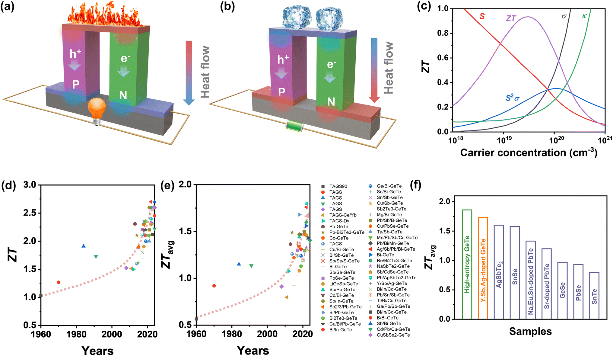
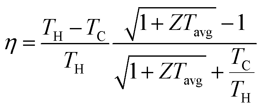
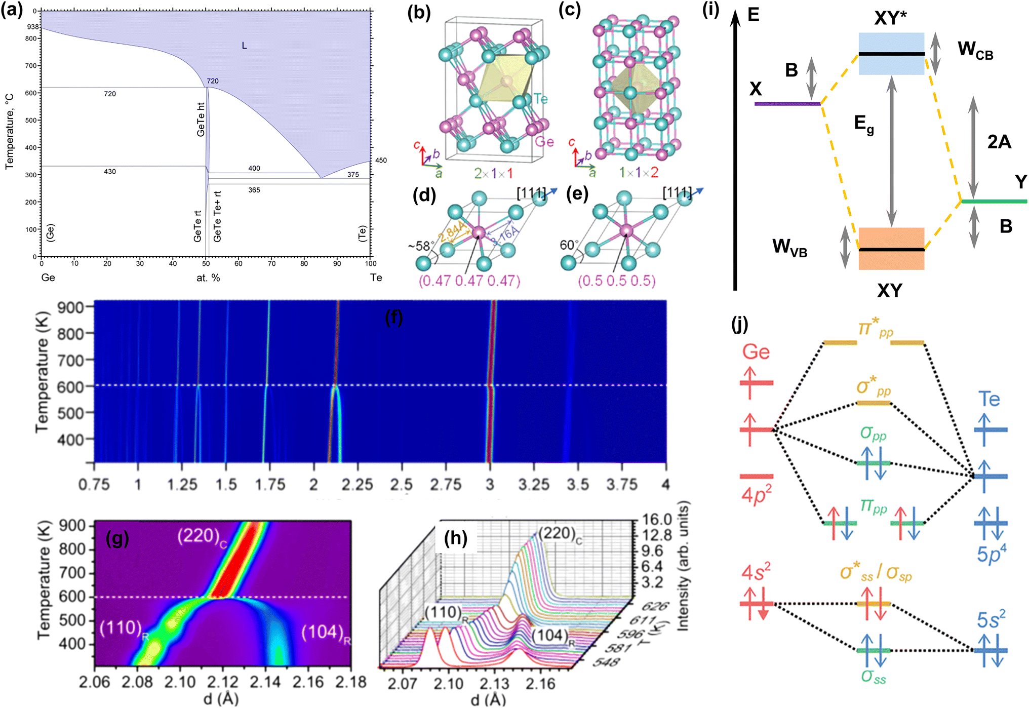


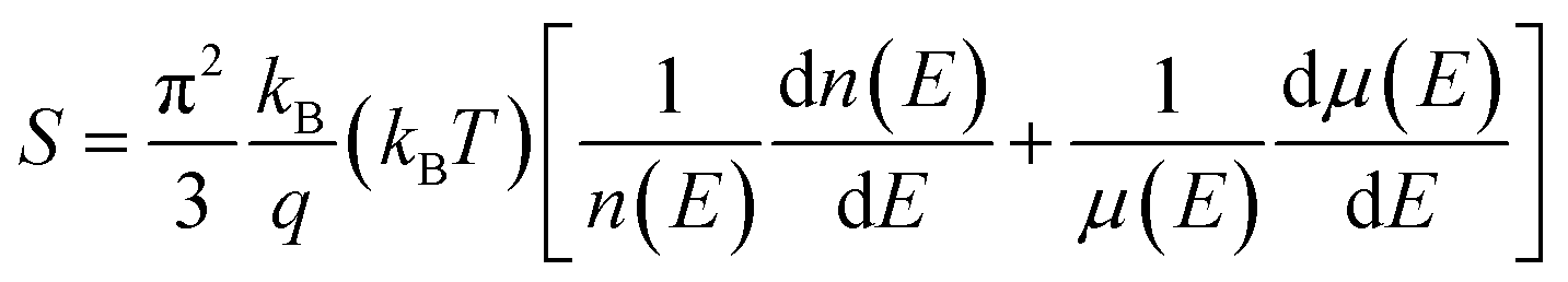
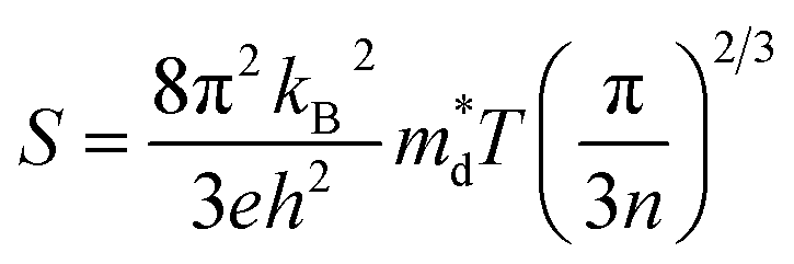
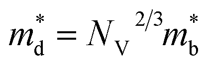
 is the density-of-states effective mass, Nv is the valence band degeneracy, and
  is the band effective mass. Basically, eqn (7) is the Pisarenko equation based on the Boltzmann's transport theory. The band degeneracy can be increased via the band convergence strategy by decreasing ΔE. As mentioned above, there is an energy gap between the L band and Σ band in rhombohedral GeTe. By introducing appropriate doping or alloying elements, ΔE can be reduced, leading to improved band degeneracy and hence the Seebeck coefficient (eqn (7) and (8)). Table 1 shows the band characteristics and electronic transport properties induced by different doping/alloying elements. It is evident that the majority of these dopants are transitional metals, while others belong to the group 15 metals and lanthanide elements. These elements have outer s-orbitals, which help to bond with electrons as they enter the GeTe crystal lattice. Zn-doped GeTe samples can be taken as an example. Upon the incorporation of the Zn atom into the crystal lattice, the outer s-orbital of the Zn atom forms covalent bonds with the anion elements. However, due to the lower energy level of the s orbitals of the Zn atom compared to that of the valence band edge, doping with Zn atoms leads to a reduction in energy of the valence band edge of GeTe, resulting in a decrease in ΔE. The band structure of (Bi and Zn) co-doped GeTe samples is shown in Fig. 5b, indicating that Zn doping induces valence band convergence by tuning s-orbital energy.116Fig. 5c shows the increased
  after Zn doping.
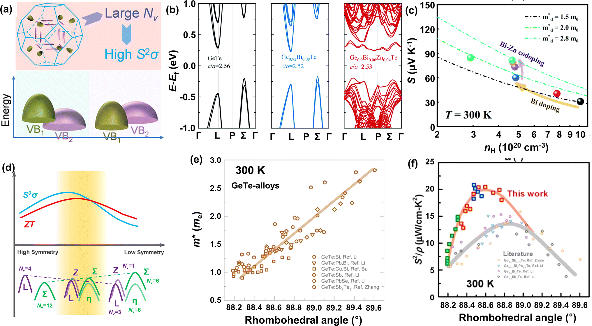
 versus the rhombohedral angle (α) for GeTe-alloys at 300 K.72 (f) Power factor versus the rhombohedral angle (α) for GeTe-alloys at 300 K.51
 of 1.2–1.9m0. It is reasonable to select promising GeTe-based thermoelectric materials within an appropriate rhombohedral phase angle. Such materials are foreseen to exhibit exceptional electrical performance.
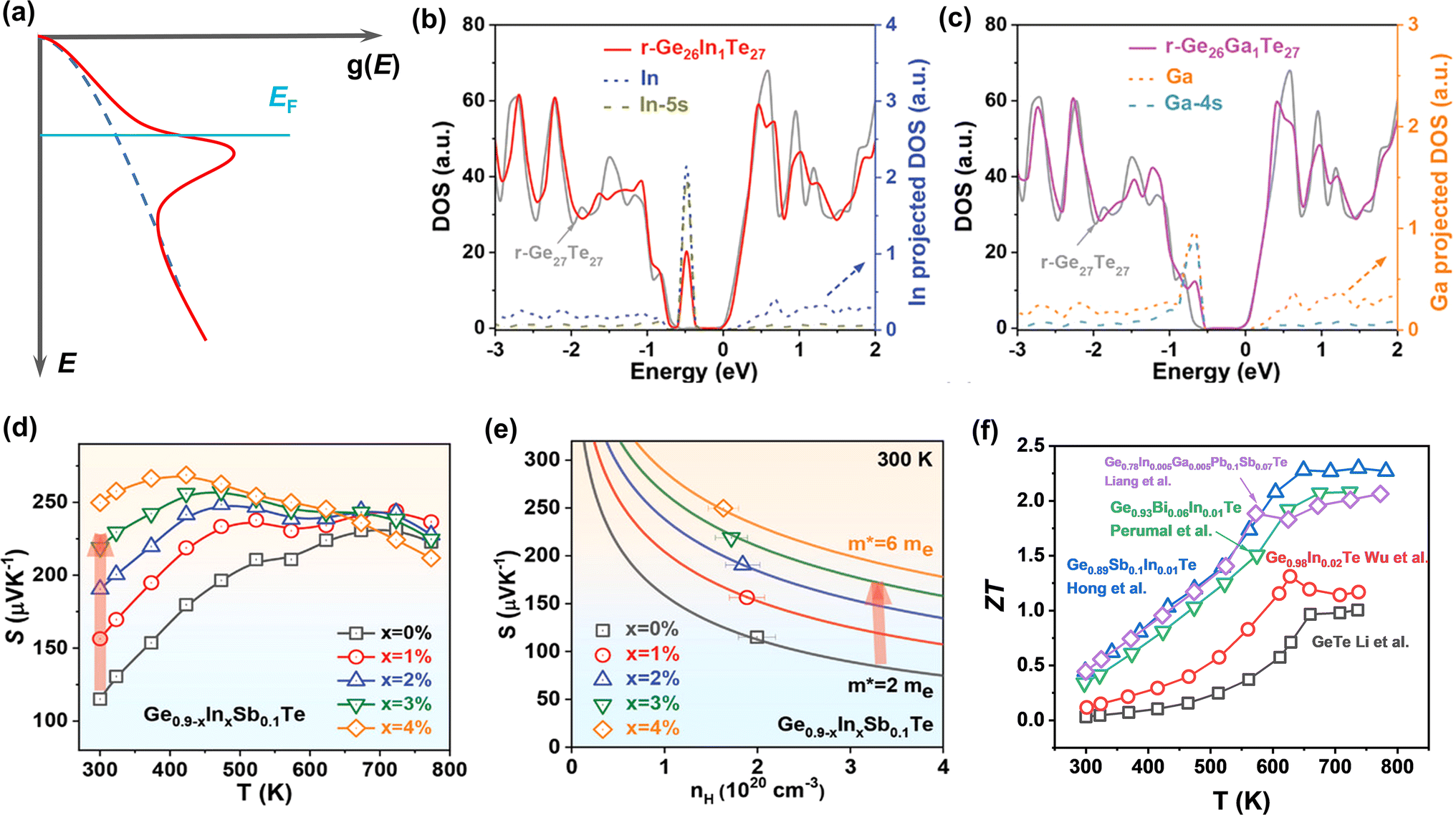
 approximation:
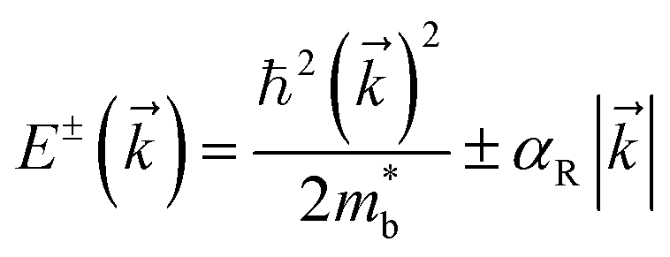


 increased at both 300 K and 780 K, indicating an improved Seebeck coefficient (Fig. 7b). According to the DFT calculations, the Rashba spin-splitting effect could be enhanced in the band structure of GeTe through Sn doping, thereby elevating the energy level of valence band edges near point Z (Fig. 7c and d).30
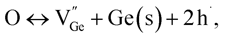
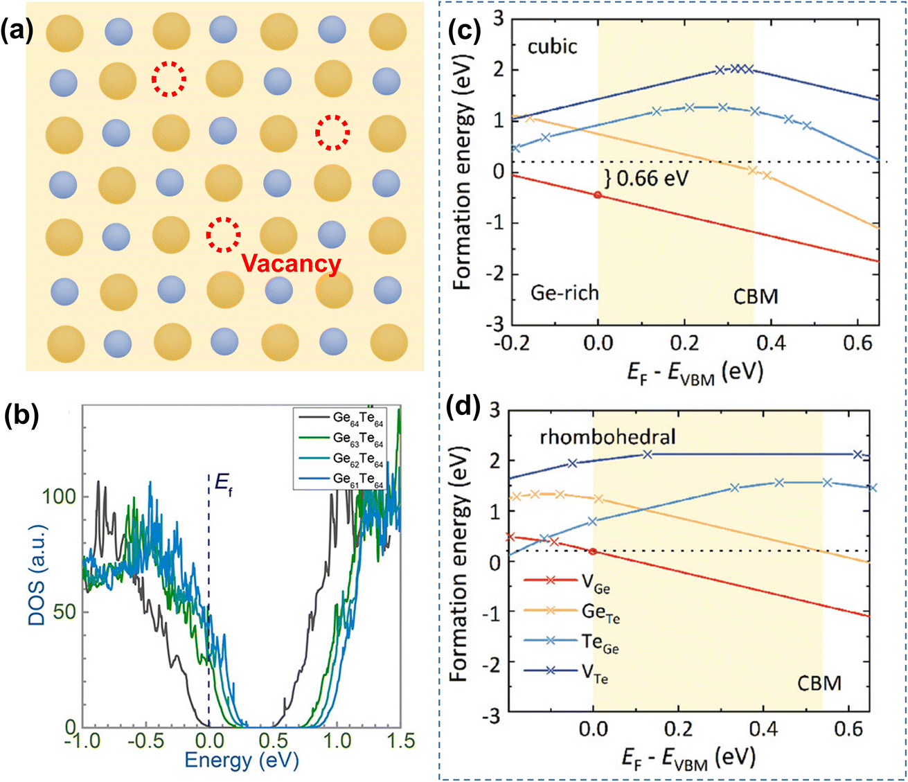

 are observed, but the carrier mobility shows an upward trend; for Bi and Sb doping,
  is improved, whilst the carrier mobility suffers from degradation as shown in Fig. 9b and c. The underlying mechanism will be discussed later.


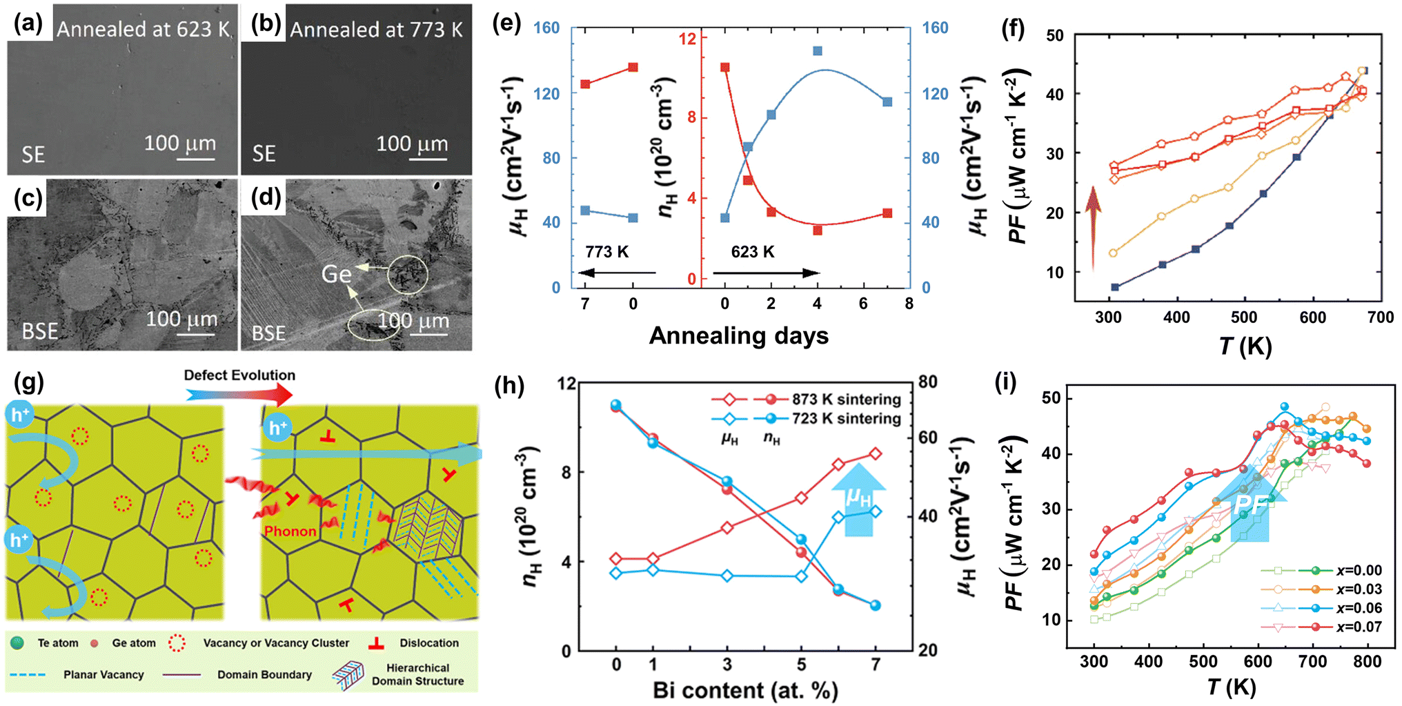

 , which is related to the density-of-states effective mass. The introduced resonant level does harm to carrier mobility due to both the increased density-of-states effective mass and reduced carrier relaxation time. To facilitate comparison of performance differences and further exploration of their potential applications, weighted mobility was utilized to classify and compare the electrical properties and performance of these elements. Weighted mobility is a descriptor that directly evaluates electronic qualities.138 Furthermore, weighted mobility is a parameter as the electrical part in the equation describing the quality factor B, which is proportional to the ZT value.139,140 An intriguing observation emerged: some elements, such as Bi (shown in Fig. 12a), exhibited nearly constant or even decreased weighted mobility, while some others, such as Cu (shown in Fig. 12b) demonstrated a gradual increase in weighted mobility with increasing doping content at 300 K.

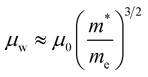


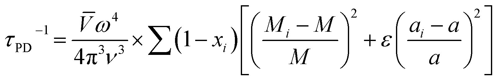
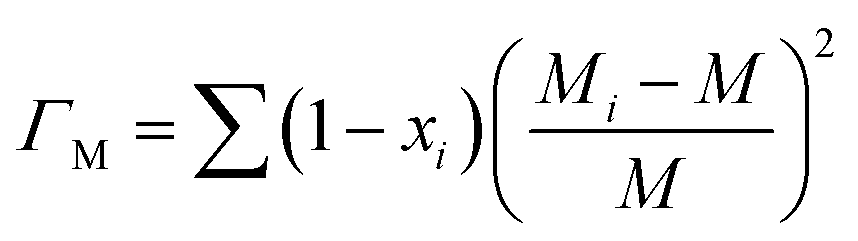
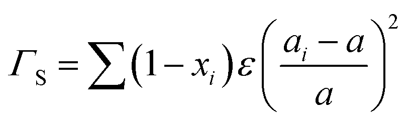
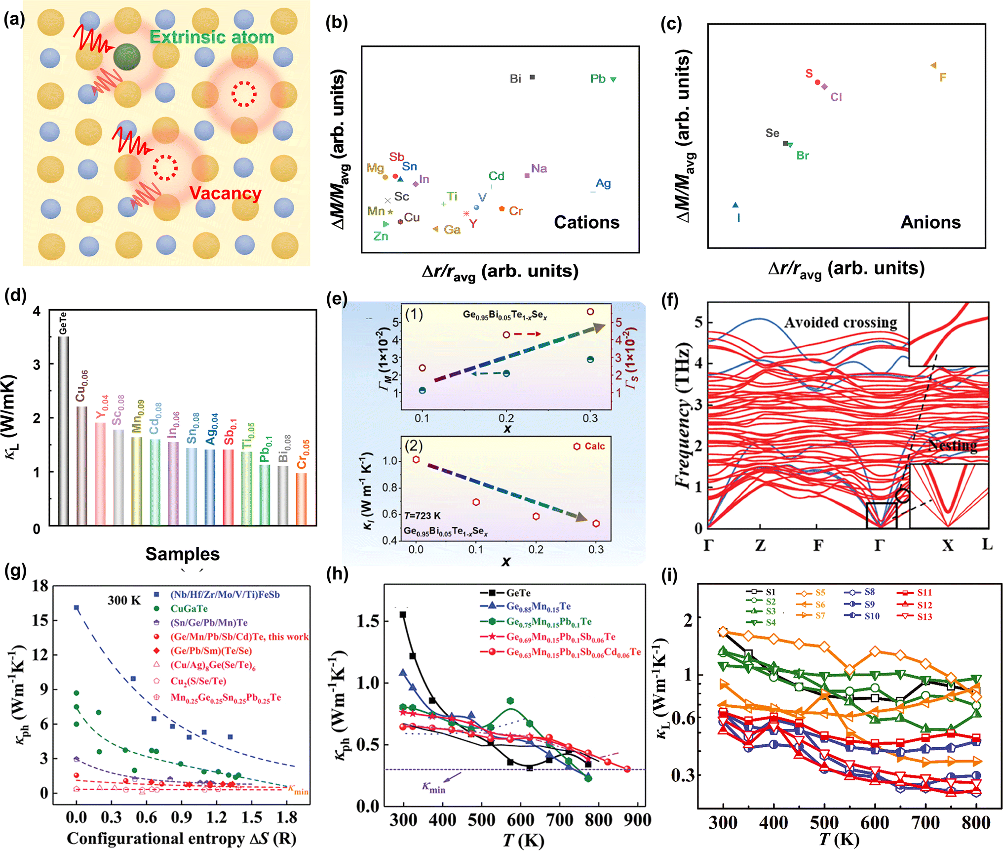
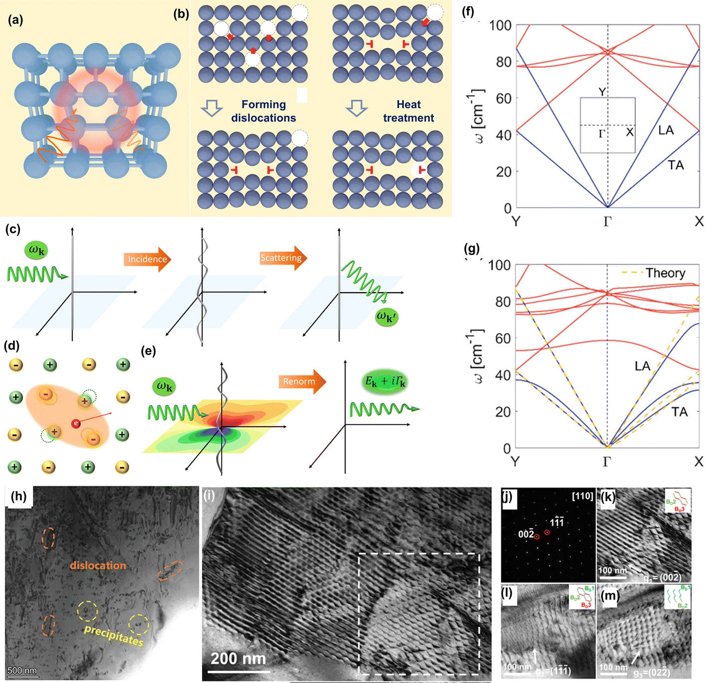

 ; in phonon renormalization, due to the long-range field of the dislocation, a phonon interacts with the dislocation even far away from the core region. The weakly interacting quasi-phonons are left with a renormalized energy Ek and a finite lifetime Γk. As shown in Fig. 17f and g, a 30 × 30 supercell was used to calculate the phonon spectra with and without a dislocation. The phonon energies show an anisotropic shift, accompanied by a reduction in phonon group velocity as shown in LA mode. This is in good agreement with the effective quasi-phonon theory prediction (yellow dashed lines) in Fig. 17g. The presence of dislocations has a significant impact on phonon propagation, thereby reducing lattice thermal conductivity. Wu et al.160 reported that by alloying AgCuTe, a number of dislocations were observed (Fig. 17h). The appearance of dislocations, combined with the precipitates, resulted in a reduced lattice thermal conductivity of 0.43 W m−1 K−1. Jiang et al.39 realized the evolution from vacancies into dislocations by controlling sintering temperature, resulting in a high-density dislocation (Fig. 17i–m); the scattering of mid-frequency phonons was enhanced, leading to reduced lattice thermal conductivity down to 0.48 W m−1 K−1.