
What is special about Y6; the working mechanism of neat Y6 organic solar cells†
Elifnaz
Sağlamkaya
 a,
Artem
Musiienko
b,
Mohammad Saeed
Shadabroo
a,
Bowen
Sun
a,
Sreelakshmi
Chandrabose
c,
Oleksandra
Shargaieva
d,
Giulia
Lo Gerfo M.
e,
Niek F.
van Hulst
ef and
Safa
Shoaee
*a
a,
Artem
Musiienko
b,
Mohammad Saeed
Shadabroo
a,
Bowen
Sun
a,
Sreelakshmi
Chandrabose
c,
Oleksandra
Shargaieva
d,
Giulia
Lo Gerfo M.
e,
Niek F.
van Hulst
ef and
Safa
Shoaee
*a
aDisordered Semiconductor Optoelectronics, Institute of Physics and Astronomy, University of Potsdam, Karl-Liebknecht-Str. 24-25, 14476 Potsdam-Golm, Germany. E-mail: shoai@uni-potsdam.de
bDepartment Novel Materials and Interfaces for Photovoltaic Solar Cells, Helmholtz-Zentrum Berlin für Materialien und Energie, Kekuléstraße 5, 12489 Berlin, Germany
cSoft Matter Physics, Institute of Physics and Astronomy, University of Potsdam, Karl-Liebknecht-Str. 24-25, 14476 Potsdam-Golm, Germany
dHelmholtz-Zentrum Berlin für Materialien und Energie GmbH, HySPRINT Innovation Lab, Department “Solution Processing of Hybrid Materials & Devices” (SE-ALM), Kekuléstr. 5, Berlin 12489, Germany
eICFO – Institut de Ciencies Fotoniques, The Barcelona Institute of Science and Technology, 08860 Castelldefels, Barcelona, Spain
fICREA – Institució Catalana de Recerca i Estudis Avançats, Passeig Lluís Companys 23, 08010 Barcelona, Spain
First published on 1st March 2023
Abstract
Non-fullerene acceptors (NFAs) have delivered advancement in bulk heterojunction organic solar cell efficiencies, with a significant milestone of 20% now in sight. However, these materials challenge the accepted wisdom of how organic solar cells work. In this work we present a neat Y6 device with an efficiency above 4.5%. We thoroughly investigate mechanisms of charge generation and recombination as well as transport in order to understand what is special about Y6. Our data suggest that Y6 generates bulk free charges, with ambipolar mobility, which can be extracted in the presence of transport layers.
New conceptsOrganic solar cells (OSCs) have attracted renewed interest with the emergence of non-fullerene acceptors (NFAs). Small molecule NFAs blended with donor polymers have rapidly advanced, reaching state of the art efficiencies of above 19% for single junctions and 20% for all-organic solution-processed tandem cells. These devices stand out by a strong complimentary absorption of the donor and acceptor components but more importantly a small energy offset at the DA heterojunction. The latter translates into a very small energy difference between the photoexcited intramolecular singlet state (S1) and the interfacial CT state (CT1), questioning the demand for a driving force for charge generation in OSCs. In this regard, we have made solar cells out of neat Y6 with 4.5% efficiency and a short circuit current of 8.4 mA cm−2. By conducting photo-Hall effect measurements and photoinduced absorption measurements, we concluded that, given the binding energy and variation of energetic landscape due to different morphologies, charge generation readily occurs in neat Y6. However, to have long-lived charges, transport layers are required to suppress recombination of the free carriers. This advancement calls for a re-evaluation of charge generation mechanisms in new materials and systems. |
Introduction
Learning from the success of fullerene acceptors, research groups synthesized non-fullerene acceptors (NFAs) from 2D planar molecules into “3D-like” molecules. With this strategy in mind, the emergence of the Y-series NFAs has dramatically pushed organic solar cells (OSCs) forward. The highest efficiencies are reported for single junctions of ternary blends in which one of the components is NFA (2,2′-((2Z,2′Z)-((12,13-bis(2-ethylhexyl)-3,9-diundecyl-12,13-dihydro-[1,2,5]thiadiazolo[3,4-e]thieno[2′′,3′′:4′,5′]thieno[2′,3′:4,5]pyrrolo[3,2-g]thieno[2′,3′:4,5]thieno[3,2-b]indole-2,10-diyl)bis(methanylylidene))bis(5,6-difluoro-3-oxo-2,3-dihydro-1H-indene-2,1-diylidene))dimalononitrile), Y6 acceptor, or one of its close derivatives. Combining Y6 with PM6 gives high and reproducible power conversion efficiencies (PCEs), between 15% and 19%.1–5 Surprisingly, high external quantum efficiencies (EQEs) are observed even with a small driving force.4,6,7When light is absorbed by organic semiconductors, the tenet holds that only excitons are intrinsically photogenerated. The excitons persist due to the strong Coulombic interaction between electrons and holes, leading to large (200–1000 meV)8 exciton binding energies (Eb). This has led researchers to combine two materials with large energetic offsets, to overcome the Eb. Such paradigms have guided the development of OSCs for the last three decades. However, the small energetic offset between Y6 and several polymers but with high efficiencies9 has sparked a lot of interest in understanding the mechanism of charge generation in neat Y6. The demand for a driving force for exciton dissociation in OSCs is ascribed to the strong Eb.10,11 Therefore, the success of high efficiencies with a small energetic offset makes Y6 intriguing as single-component materials and calls for a re-evaluation of charge generation mechanisms in new materials and systems.
Formation of polaron pairs in neat Y6 films has now been reported by several groups.12,13 Transient absorption studies have suggested that in neat Y6, excitons are delocalised, or form an intra-moiety intermediate state.13 Interestingly, all existing time-resolved spectroscopic studies indicate that both exciton and polaron pairs are simultaneously created within the time resolution of the experiment;14 however, since both the features inconveniently overlap in the spectral region, and the free charges are reported to be very short-lived, it is challenging to understand the mechanism of charge generation. This puzzling observation has led to a substantial debate about the physical mechanisms underlying ultrafast exciton dissociation in neat Y6. Different scenarios can be invoked, including field-assisted photogeneration of the charge transfer state, the rapid formation of CT by exciton dissociation either at interlayer interfaces or due to energetic cascade caused by aggregation and different crystallinity and morphology of Y6 or, CT formation from delocalized coherent excitations due to low Eb. In this regard Zhu et al. have estimated the Eb of Y6 in the solid phase to have values of −0.11 to 0.15 eV.15 Such small values are debatable compared to cyclic voltammetry measurements where the exciton binding energy of around 0.3 eV can be estimated.16 In addition, another drawback of neat devices is the difficulty in obtaining the optimized phase separation between donor (D) and acceptor (A) segments in a single material, resulting in severe charge recombination and low charge transport efficiency, as reported by Hodgkiss and co-workers.12
To reflect the importance of all of these exhilarating findings, we fabricated single component Y6 devices with an efficiency of 4.5%–the highest PCE reported for single material small molecule OSCs.17–19 We use a combination of electroluminescence quantum efficiency (EQEEL), photoluminescence (PL), electroluminescence (EL), temperature dependent quasi-steady state absorption spectroscopy (PIA), Hall and photo-Hall measurements, time-delayed collection field (TDCF), and bias-assisted charge extraction (BACE) to analyse the device physics and identify the mechanism of charge generation and recombination pathways. Although exciton dissociation has been reported on ultrafast timescales,12 herein we observed that long-lived charge is only present when Y6 is interfaced with at least one transport layer. Our Hall measurements, PIA and TDCF data indicate that long lived free charges are generated in the bulk and are field independent, while the field dependent PL measurements further confirm extraction of free charge. We further found that charge transport is bipolar and very efficient, 2 × 10⁻³ cm2 V−1 s−1 and 0.9 × 10⁻³ cm2 V−1 s−1 for electrons and holes, respectively. However, despite these merits, recombination of free carriers in the neat Y6 device is several folds faster than that in the state-of-the-art PM6:Y6 blend. We also investigated single neat devices of (2,2′-((2Z,2′Z)-((12,13-bis(2-ethylhexyl)-3,9-diundecyl-12,13-dihydro[1,2,5]thiadiazolo[3,4e]thieno[2′′,3′′:4′,5′] thieno[2′,3′:4,5]pyrrolo[3,2-g] thieno[2′,3′:4,5]thieno[3,2-b]indole-2,10-diyl)bis(methanylylidene))bis(3-oxo-2,3-dihydro1H-indene-2,1-diylidene))dimalononitrile), Y5, and (2,2′-((2Z,2′Z)-((12,13-bis(2-butyloctyl)-3,9-dinonyl-12,13-dihydro-[1,2,5]thiadiazolo[3,4-e]thieno[2′′,3′′:4′,5′]thieno[2′,3′:4,5]pyrrolo[3,2-g]thieno[2′,3′:4,5]thieno[3,2-b]indole-2,10-diyl)bis(methanylylidene))bis(5,6-dichloro-3-oxo-2,3-dihydro-1H-indene-2,1-diylidene))dimalononitrile), eC-9 for comparison. From the findings we suggest that the given external quantum efficiency (EQE) in Y6 is due to bulk charge generation in addition to the exciton dissociation at transport layer interfaces in Y6, good charge transport and the presence of transport layers to spatially separate the free carriers from one another.
Results and discussion
In the investigated devices, Y6 is inserted between ITO and Al contacts, together with electron and hole transport layers (ETLs and HTLs, respectively), which improve the contact selectivity and device performance. 3-[6-(Diphenylphosphinyl)-2-naphthalenyl]-1,10-phenanthroline (Phen-NaDPO or DPO) is used as an ETL, and copper(I) thiocyanate (CuSCN) is used as a HTL. As shown in Fig. 1a, a 60 nm layer of CuSCN is used adjacent to Y6, as a hole transport layer while CuSCN does not absorb to generate any charges.14 Further details about the device structure can be found in the experimental section. The best device performance is achieved when 0.5% 1,8-diiodooctane (DIO) in chloroform (CHCl3) is added as an additive to the Y6 solution. The open-circuit voltage (VOC) in both cases is rather low as compared to the Y6's optical gap (Eopt) of 1.7 eV.20 The biggest difference with the addition of the additive is reflected in the increase in the average short-circuit current density (JSC) from 5.3 to 8.4 mA cm−2 and in the fill-factor (FF) which becomes 65% compared to 55% (Fig. 1b and Table 1). Yet interestingly we did not observe any sub-gap absorption peaks in the measured EQE spectra which could be attributed to the formation of charge transfer (CT) states at the Y6 and interlayer interfaces (Fig. S1b, ESI†) and the thickness dependent data show an increase in JSC and performance with increasing junction thickness (Fig. S2, ESI†). In this paper we focus on understanding the mechanism of charge generation with and without DIO, reflecting on the JSC and FF. | ||
| Fig. 1 (a) Energy levels (materials not in contact with each other) of the CuSCN21 hole transport layer, small molecule acceptor Y6,22 Phen-NaDPO23 electron transport layer and of the electrodes21 taken from the literature. (b) Current density–voltage (J–V) characteristics of a regular device with a 100 nm neat Y6 active layer with and without the DIO additive measured under simulated AM1.5G light (solid lines) and in the dark (dashed lines). | ||
| Additive | J SC [mA cm−2] | V OC [V] | FF [%] | PCE [%] | ΔVOC,nr |
|---|---|---|---|---|---|
| With DIO | 8.4 | 0.79 | 65 | 4.4 | 0.3 |
| Without DIO | 5.3 | 0.82 | 55 | 2.4 | 0.26 |
To elucidate the free charge separation mechanism in the neat Y6 device, we employed the Hall effect and photoconductivity measurements on 100 nm thick neat Y6 films on glass with and w/o DIO. Photo-Hall measurements were carried out by monitoring the Hall and conductivity signal with increasing illumination intensity. The increase in photoconductivity indicates the formation of free charge carriers. The charge carrier concentration can be calculated form the product of the photoconductivity and mobility (see Note S1, ESI†). In the dark measurements, we calculated the carrier density with the assumption that the Hall signal originates from excess electrons. The films w/o DIO had an electron density of 3.8 × 1013 cm−3. The solvent additive DIO introduces a major increase in the electron density, estimated to be 7.4 × 1014 cm−3. Further, under illumination with an excitation energy of 1.7 eV, both films exhibited an increase in the photoconductivity due to the increased carrier concentration, which points towards bulk charge photogeneration in neat Y6 films on glass (Fig. 2a).
 | ||
| Fig. 2 (a) Photoexcited charge carrier concentration of 100 nm thick neat Y6 films on glass was estimated from intensity dependent 4-probe Hall conductivity measurement with an excitation energy of 1.7 eV. (b) Photo-induced absorption spectra of the semi-transparent Y6 device with and w/o DIO measured from the electrode-free area. | ||
We conducted quasi-steady-state photoinduced absorption (PIA) spectroscopy to assess the efficiency of free carriers in Y6 with and without transport layers. We had previously demonstrated that PIA can be an effective assay of yield of free carriers.24 The technique monitors the differential absorption upon modulation of the intensity of the quasi steady-state illumination and therefore probes long-lived species only. Fig. 2b shows the PIA spectra measured for the CuSCN/Y6/DPO sample under open-circuit conditions. For Y6 films sandwiched between the interlayers we observe the GSB signal to be around 850 nm and the PIA band in the region around 1000 nm. Given that the technique operates on long time scale measurements (μs–s), unique absorption features of polarons are those of free carriers and not charge transfer states or excitons, indicating that long-lived charges are present in the sample. In particular it is observed that the DIO sample exhibits a reasonable amplitude. The amplitude of the signal is proportional to carrier density, n through the equation 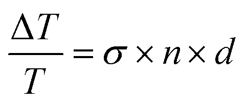 ;24 thus the PIA spectra insinuates that the DIO sample has a higher free carrier density. On the other hand, films of Y6 without transport layers gave negligible signals due to the resolution of the system. This highlights the important role of the transport layers in spatially separating and stabilising the free carriers in the photoactive layer; thereby avoiding fast recombination.12
To understand the mechanism of charge generation in neat Y6 and the difference in the PIA amplitudes between DIO and no DIO samples, we performed photoluminescence (PL) measurements to elucidate if excitons limit charge generation. In order to investigate the role of excitons, we fabricated thin Y6 (15 nm) films with and without the transport layers, to measure photoluminescence quantum yield (PLQY) and thereby assess exciton quenching. As shown in Fig. 3a, the PL of neat Y6 films prepared from CHCl3 only, gets quenched by 76% when interfaced with both CuSCN and Phen-NaDPO layers, while when Y6 is processed from CHCl3 and DIO, and sandwiched between CuSCN and Phen-NaDPO, we observed the Y6's singlet exciton to be quenched by 98% (see Fig S5 in for thickness dependent PLQ data, (ESI†)).
 | ||
| Fig. 3 Absolute photoluminescence spectra of the Y6 films with 15 nm thickness (a) without and (b) with DIO additive showing PL quenching when in contact with transport layers, measured in an integrating sphere. 2D GIWAXS images of (c) without and (d) with DIO Y6 films, where the q values are calculated with azimuthal integration. | ||
Spatially and time resolved fluorescence microscopy measurements25 were conducted on 100 nm Y6 films with DIO and w/o DIO in order to compare the exciton diffusion coefficient and the exciton lifetime. The calculated exciton diffusion length of the Y6 with DIO film is only 7 nm longer than that of Y6 w/o DIO (∼56 nm and 49 nm, respectively) (see Note S2 and Fig. S6, ESI†). The slight increase in the diffusion length can arise from an increased aggregation in the sample. Thus, we characterized the morphology of the 100 nm neat Y6 films with and w/o DIO using grazing incident X-ray scattering (GIWAXS) measurements. As shown in Fig. 3c and d the Y6 films with DIO exhibited an enhanced long-range order. The calculated d spacing (d = 2π/p) for the π–π stacking was 0.349 nm for the Y6 film with DIO and a slightly longer d of 0.353 nm for the w/o DIO film was detected (Fig. S7, ESI†), which shows that aggregation is enhanced in the DIO sample.26,27
Consistent with the reports on aggregation of Y6,28,29 our result (in particular the thickness dependent JV data in Fig. S2, ESI†) favours a picture of aggregation-dependent energy levels,30,31 thereby enabling an energy cascade which facilitates exciton dissociation in the bulk (in addition to interfacial exciton dissociation at the TL) and further drives charges out from the more disordered domains into a more-crystalline domain of Y6. But it should be noted that while we see quenching of Y6 emission when interfaced with transport layers, we cannot rule out partial quenching in the neat Y6 film on glass. The enhanced PL quenching of the DIO sample compared with no DIO sample just on glass, indicates that some exciton dissociation readily occurs in the neat film on glass without the aid of transport layers. This insinuates that the exciton dissociation occurs both at the TL interface and in the bulk of Y6. Furthermore, very strikingly, the complete device under different bias conditions (VOC, JSC and reverse bias) was found to have decreasing PL intensity with increasing reverse bias (Fig. 4a and b) indicating that PL intensity in the neat Y6 device is a field assisted process.
 | ||
| Fig. 4 (a) Photoluminescence spectra of a device with a 15 nm Y6 active layer (a) with no additives and (b) with the DIO additive in the ITO/CuSCN/Y6/Phen-NaDPO/Al structure, under VOC and JSC conditions and under several different applied negative bias conditions. (c) Bias-dependent free charge generation (symbols, left axis) for an inverted Y6 device measured with TDCF for an excitation of 2.07 eV with a low fluence of 0.05 μJ cm−2 and Vcoll = −2 V. For comparison, the current density–voltage characteristics of the device under simulated AM1.5G light are also shown (solid lines, right axis). (d) Bimolecular recombination coefficient as a function of charge carrier density, obtained from BACE measurements for Y6 of 100 nm thickness without the DIO additive (solid pink squares), and with the DIO additive (solid green squares). | ||
Following the observation of field dependent PL intensity, we investigated if charge generation too is field dependent, utilizing TDCF experiments as a function of electric field. The experimental details on TDCF have been described elsewhere.32 In short, the device was excited with a short laser pulse (∼5 ns) while being held at a given pre-bias (Vpre). After a delay time of 6 ns (once the laser is switched off) all charges were extracted by applying a high reverse collection bias (Vcoll). To ensure that non-geminate losses are insignificant during the measurement, we applied a sufficiently large Vcoll of −2 V and the laser intensity was chosen to be low enough to lie in a linear regime (the extracted charge is strictly proportional to the laser fluence) where second order recombination is negligible.33 Then, the total extracted charge (Q) is a direct measure of the efficiency of free charge generation under these conditions. Fig. 4c shows the results of such a measurement for both DIO and w/o DIO devices (with the transport layers), where Vpre is swept from reverse bias to VOC. Here, the excitation energy was 2.38 eV. In both cases, we found that the total charge Qtot does not depend on the applied bias Vpre, even when approaching VOC, meaning that the photocurrent does not suffer from increased geminate recombination when the internal field is decreased. Furthermore, the field independent charge generation mechanism suggests that the field dependent PL, is not due to exciton dissociation but rather due to extraction of free carriers, whereby with increasing reverse bias, extraction is improved and thereby fewer charges are left to recombine through the reformed exciton (reduced PL intensity).
In blends, it has been argued that CT separation can be assisted by various processes such as driving force,31,34 entropy,35 high local mobilities,36 and delocalization of charges on aggregated phases of the donor and/or the acceptor.31,37,38 In addition, several recent papers highlighted the role of energetic disorder in providing low energy sites for the dissociation of CT states in blends or even singlet excitons in neat organic semiconductors. For instance, Hood and Kassal concluded that a Gaussian disorder σ of 100 meV is sufficient to reduce the free-energy barrier to ca. 25 meV, meaning that thermal energy is sufficient to dissociate CT states at room temperature.35
Accordingly, we performed temperature dependent space-charge limited current (SCLC) experiments in electron- and hole-only devices to quantify mobility at room temperature and the energetic disorder in Y6 devices (since this approach has been shown to be sensitive to the shape and width of the DOS) (Fig. S8, ESI†). Energetic disorder obtained using the Gaussian disorder model (GDM) and mobility values are tabulated in Table 2. Although the combined disorder is rather large, however other NFAs also exhibit similar or even larger values (see Table S4, ESI†) of energetic disorder while not exhibiting efficient charge generation or device performance in neat layers. Therefore, such disorder values cannot be solely responsible for energetic disorder as the main driving force for charge separation.
| Additive | μ e [cm2 V−1 s−1] | σ LUMO [meV] | μ h [cm2 V−1 s−1] | σ HOMO [meV] |
|---|---|---|---|---|
| With DIO | 2.1 × 10⁻³ | 70 | 9.6 × 10⁻⁴ | 76 |
| w/o DIO | 2.4 × 10⁻³ | 71 | 1.8 × 10⁻⁴ | 74 |
Now turning to investigate non-geminate recombination in the complete device and to determine the recombination coefficient krec as a function of carrier density, we employed bias assisted charge extraction (BACE). In BACE, the device is held at VOC under steady-state illumination and as soon as the light is turned off, a high reverse bias is applied to extract all charges. A recombination order close to 2 rules out trap-assisted recombination. The analysis of the recombination data according to R = k2ncoll2 as shown in Fig. 4d yields bimolecular recombination coefficient values of 2 × 10⁻¹¹ cm3 s−1 and 1 × 10⁻¹⁰ cm3 s−1 for Y6 with and without DIO, respectively. We noted that these values are up to one order of magnitude higher than what is reported for state of the art PM6:Y6, 7 × 10⁻¹² cm3 s−1 to 2 × 10⁻¹¹ cm3 s−1.39,40
The efficiency limitation that comes with the high k2 value in the sample without DIO can be illustrated with numerical drift-diffusion simulations. In Fig. 5 we have shown that by using our experimental data as input to simulation, we fully reproduce the JV curves of the neat Y6 devices with and without DIO, using our measured parameters (a summary of all simulation parameters is given Table S3, ESI†). Although the difference in recombination between the two devices can be explained from the hole mobility difference in improving the competition between extraction vs. recombination, however we should not underestimate the role CuSCN plays. In comparison, recombination of free carriers in Y6 on glass (without transport layers), as reported by Hodgkiss and co-workers, is on the timescale of 100 pico-seconds.12 The difference between the lifetimes obtained for the films on glass (as reported by Hodgkiss and co-workers) and our measurements with TLs, suggests that in the presence of transport layers, the free charges generated in the bulk can travel to the respective transport layer and suppress recombination.
 | ||
| Fig. 5 Current density–voltage characteristics of 100 nm Y6 devices with and w/o the DIO additive with structure ITO/CuSCN/Y6/Phen-NaDPO/Al (fully reflecting 100 nm) and a device area of 6 mm2 under simulated AM1.5G light. Open squares are the experimental results and the solid lines are the drift-diffusion simulation results generated by using the experimentally determined values for k2 and values close to the measured μe/h. A shunt resistance (Rshunt = 8.6 × 10² Ω cm2) and series resistance (Rs = 1 Ω cm2) were implemented. | ||
By comparing the device performance of Y6 with those of Y5 and eC-9 (see Fig. S11 and Table S4 for details, ESI†) we conclude that our results question charge thermalisation in a broad DOS range as the origin of efficient charge generation in our Y6 neat device. Instead, they favour a picture with aggregation-dependent electron affinity, providing an energy cascade to dissociate the excitons and drive electrons and holes out from the more disordered domains into the well-crystallized domains of neat Y6. The structure of the core unit of Y6 is quite different from that of traditional acceptor (A) donor (D) acceptor NFAs.41 Y6 has a unique ADA′DA structure and the core is angular with an electron-deficient benzothiadiazole fragment at the centre. It has four side chains, with two attached to the inside pyrrole rings and two attached to the outside thiophene rings. Due to the steric repulsion between the two inside alkyl chains, the molecular plane of Y6 shows a certain degree of twist, and the inside alkyl chains move out of the plane to mitigate over crystallisation. Furthermore, the two outside alkyl chains restrict the rotation of the 2-(5,6-difluoro-3-oxo-2,3-dihydro-1H-inden-1-ylidene)malononitrile (DFIC) end units, leading to a higher degree of conformational rigidity and uniformity for the Y6 acceptor. This structure results in a large quadrupole moment, which causes band bending and may facilitate and contribute to charge separation.42 Furthermore, in comparison to NFAs reported earlier, Y6 films have a more preferential face-on orientation, and clusters of Y6 are better connected, encouraging more efficient transport. Single crystal analysis also revealed that Y6 undergoes rather unique peaking to form a 3D network for efficient charge transport43 consistent with our highly balanced transport data. Coupling charge generation properties (interfacial and bulk) with efficient transport mobilities for both holes and electrons in Y6, results in long-lived free carriers only when the charges are spatially separated from one another in the bulk with the aid of the transport layers.
Conclusions
Combining photo-Hall measurements and PIA, we showed that the Y6 material generates long-lived free charges upon light excitation (albeit the conventional two-step process). We have characterized full devices consisting of a single active layer component with a PCE of 4.5%, and showed that the free charge generation is a field independent process. Furthermore, by comparing Y6 devices with and without the DIO additive, we explained the increase in the JSC by enhanced charge generation caused by more exciton dissociation due to aggregation and better extraction of holes due to higher mobility. The improved FF of the Y6 devices with the additive is explained by balanced charge carrier mobility and reduced recombination. The bimolecular recombination is suppressed in the Y6 devices with DIO, as it appears in the bias assisted charge extraction measurements. In light of these drastic changes in the device characteristics with the DIO additive, we consider that there is a morphology dependent energy cascade in the Y6 films.Experimental
Sample preparation
The small acceptor molecule Y6 were purchased from 1-Material Inc. Copper thiocyanate (CuSCN), diethyl sulfide (DES), chloroform (CHCl3), 1,8-diiodooctane (DIO), 3-[6-(diphenylphosphinyl)-2-naphthalenyl]-1,10-phenanthroline (Phen-NaDPO), and methanol were purchased from Sigma Aldrich. 1-Chloronaphthalene was purchased from Alfa Aesar. 2,9-Dimethyl-4,7-diphenyl-1,10-phenanthroline (BCP) the devices with a regular configuration were fabricated with the structure ITO/CuSCN/Y6/Phen-NaDPO/Al. Patterned ITO (Lumtec & PsiOTech Ltd) substrates were cleaned in a beaker with Hellmanex at 75 °C for 1 h, wiped with paper tissues and then taken to an ultrasonic bath to proceed to cleaning with Hellmanex for 20 min, deionized water for 20 min, acetone for 15 min and isopropanol for 15 min, followed by microwave plasma treatment (4 min at 200 W). 26 mg ml−1 CuSCN was dissolved in DES at 60 °C for 1 h and spin coated onto ITO at 2500 rpm. Y6 solutions were prepared either with pure CHCl3 or 0.5% DIO (v/v, DIO/CHCl3) at 20 mg ml−1 concentration. 100 nm of the active layer was spin coated onto the CuSCN hole transport layer at 1700 rpm. The Phen-NaDPO electron transport layer and Al electrode were evaporated under a 10−6–10−7 mbar vacuum. For PL measurements the neat films and films with transport layers were spin coated onto the clean glass substrates.Current–voltage characteristics
JV curves were measured using a Keithley 2400 system in a 2-wire source configuration. Simulated AM1.5G irradiation at 100 mW cm−2 was obtained using a filtered Oriel Class AAA xenon lamp and the intensity was monitored simultaneously with a Si photodiode. The sun simulator was calibrated with a KG5 filtered silicon solar cell (certified by Fraunhofer ISE).Time delayed collection field (TDCF) and bias assisted charge collection (BACE)
In TDCF, the device was excited with a nanosecond laser pulse from a diode pumped Q-switched Nd:YAG laser (NT242, EKSPLA) with a 5 ns pulse duration at a typical repetition rate of 500 Hz. To compensate for the internal latency of the pulse generator, the laser pulse was delayed and homogeneously scattered in an 85 m long silica fibre (LEONI). The devices held at different pre-bias voltages (Vpre) were subsequently switched to a large negative bias (Vcoll) (−2 V) to collect the photogenerated charges with the laser pulse. Vpre and Vcoll were set using an Agilent 81150A pulse generator through a home-built amplifier, which was triggered with a fast photodiode (EOT, ET-2030TTL). The current flowing through the device was measured via a 10 Ω resistor in series with the sample and recorded with an oscilloscope (Agilent DSO9104H). Great care was taken to avoid free carrier recombination prior to extraction. Therefore, the bias was ramped-up (∼2.5 ns) very fast.In BACE, the devices were held under steady state conditions by illuminating with 1 W, 638 nm and 520 nm laser diodes (insaneware) with a switch-off time of ∼10 ns. The laser diode was operated at 500 Hz with a duty cycle of 50%, such that illumination lasted 1 ms and the diode was switched off also for 1 ms. Right after switching off the laser, a high reverse bias was applied to the sample using the same fast pulse generator (Agilent 81150A) as in TDCF measurements, allowing a fast extraction time of 10−20 ns. The current transients were measured via a 10 Ω resistor in series with the sample and recorded with an oscilloscope (Agilent DSO9104H).
Photoluminescence (PL)
PL emission spectral measurements were recorded with an Andor Solis SR393i-B spectrograph with a silicon detector DU420A-BR-DD and an indium gallium arsenide DU491A-1.7 detector. A calibrated Oriel 63355 lamp was used to correct the spectral response. The film under study was excited with a 520 nm laser (insaneware) under negative bias open-circuit (OC) and short-circuit (SC) conditions. PL spectra were recorded with different gratings with central wavelengths of 800, 1100, and 1400 nm and merged afterwards.In absolute PL measurements, the same laser was used together with an optical fibre that goes into the integrating sphere that holds the sample. Measurements were made with 1 sun intensity. The spectra were recorded using an Andor Solis SR393i-B spectrograph connected to an integrating sphere with another optical fibre. A calibrated Oriel 63355 lamp was used to correct the spectral response (same as for EL and PL measurements above), which was shone into the integrating sphere. The spectral photon density was obtained from the corrected detector signal (spectral irradiance) by division through the photon energy (hv), and the photon numbers of the excitation and emission were calculated from the numerical integration, using a MatLab code. Great care was taken to avoid the measured PLQY values with the integrating sphere being influenced by waveguided light that is outcoupled through the sides of the substrate, and thereby we taped the four sides of our glass substrates with black tape.
AC Hall measurements
Hall measurements44 were performed in a 4-probe configuration with a Lake Shore 8400 Hall system. All 4 probe combinations showed a linear IV response and an ohmic contact signature. We used an AC magnetic field (100 mHz) and a lock-in amplifier to enhance the Hall signal. The current through the samples (in the range 0.1–2 nA) was supported by a current source. The Hall data are fully consistent with 4-probe (4c) conductivity measurements.Photo-Hall and photoconductivity measurements
To gain insight into the charge transport under illumination, we further studied thin-film conductivity and Hall effects by illuminating them with 1.7 eV light and intensity close to 1 sun. The photoexcited electron concentration is calculated according to Hall effect mobility (Δn = PhC/(e·μh) due to a better signal-to-noise ratio. The lifetime (τe) and diffusion length (L) were calculated using the following relations and
and 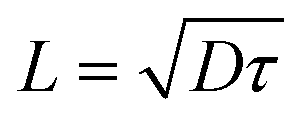 , where G is the generation rate and D is the diffusion constant. Due to the high thickness of the samples (100 nm), we assumed total absorption of light. The decrease in Hall mobility in the sample with additives is explained by the participation of free holes in charge transport, compensating free electron signals:45
Photoinduced absorption (PIA)
In PIA measurements, the photoexcitation of a 405 nm continuous wave laser diode (Spectral Products) is modulated at a frequency of 570 Hz using an optical chopper (Thorlabs MC2000B). In EM measurements, a square voltage with a frequency fixed at 370 Hz and a tunable amplitude provided using a function generator (Keysight 33210A) is applied to the device. The white light emitted from a tungsten halogen lamp is optically directed into a monochromator (Spectral Products DK240), and the monochromatic light emitted from the monochromator is used as the probe light, and focused on the studied device to overlap with the photoexcitation light. The change in the transmitted probe light ΔT induced by the photoexcitation in PIA and the dark injection in EMIA is recorded using a Si photodiode (Thorlabs) and a lock-in amplifier (SR830) and then corrected by background subtraction. The transmitted probe light T through the unexcited sample is measured by using another optical chopper (Thorlabs MC2000B) to modulate the probe light, the same photodiodes and the lock-in amplifier. Our PIA system has a sensitivity on the order of 10−7.Space charge-limited currents (SCLCs)
Electron-only devices were prepared in the ITO/ZnO/Y6 (170–200 nm)/Phen-NaDPO (10 nm)/Al (100 nm) configuration. ZnO nanoparticle dispersion in isopropanol (Avantama N-10) was filtered with a 0.45 μm polytetrafluoroethylene filter and spin coated onto ITO at 5000 rpm for 40 s in air and annealed at 120 °C for 30 min. Hole-only devices with the configuration ITO/MoO3 (8 nm)/Y6 (170–200 nm)/MoO3 (8 nm)/Ag (100 nm) were prepared by evaporating MoO3 on top of ITO. Then, the active layer was prepared as for solar cell devices, followed by evaporation of 8 nm MoO3 under a 10−6–10−7 mbar vacuum.For temperature-dependent measurements, the devices were loaded into a liquid nitrogen-cooled cryostat (VPF-100 Janis) and the temperature was adjusted in a range of 220 K to 320 K using a temperature controller (Lakeshore 335). JV data were measured using a Keithley 2400 source meter in a two-wire configuration.
External quantum efficiency (EQEPV) and absorbance
EQEPV was measured using a home-made setup containing a quartz tungsten halogen lamp, a Thorlabs MC2000B optical chopper at a frequency of 165 Hz, a Bentham TMC300 monochromator, a lock-in amplifier (SR830) and a preamplifier (SR570). The system was calibrated using a standard silicon detector from Enlitech. For EQE measurements as a function of temperature, the sample was placed in the same cryostat as used for JV measurements and the modulated light from the monochromator was focused on the active area of the sample. The electrical signal of the sample was sent to the preamplifier and then the lock-in amplifier. The voltage was applied to the sample from the preamplifier. Absorbance was measured with a Varian Cary 5000 in transmission and reflection model with an integrating sphere.Spatially and time resolved fluorescence microscopy
A 150 fs-pulsed Ti:sapphire laser with a repetition rate of 76 MHz and wavelength 800 nm is used as excitation source. A telescope with a pinhole spatially cleans the beam, while prism compressors compensate for temporal dispersion. The beam is scanned over the sample plane with a galvo-mirror followed by a second telescope. A Nikon Plan APO λ NA 1.40 60× oil immersion objective focuses the beam to a spot of FWHM of 390 nm. In the detection part, fluorescence is confocally collected using a single photon avalanche diode (SPAD) from the MPD series (instrument response function of 50 ps) in reflection through an 830 LP filter and a 15 μm pinhole corresponding to a central spot size of 250 nm diameter in the sample plane. To acquire 2D spatio-temporal maps, the excitation spot is moved away from the detection spot at a well-known distance. Excitons need a certain time to travel the distance between the generation and the collection spot. This results in a time delay which can be identified from an effective increase in the lifetime of fluorescence. The collected fluorescence intensity I(x,t) is then integrated every 20 ps at each scanning position (every 100 nm) along the cross-section of the excitation profile.25Grazing-incidence wide-angle X-ray scattering (GIWAXS)
Measurements were conducted at the μSpot beamline of the BESSY II synchrotron in Berlin with a 9 keV beam incident on the sample at an angle of 0.1° and a photon flux of 1014 cm−2 s−1. The diffracted beam was detected using an Eiger 9M detector and detector frames were integrated azimuthally using a LaB6 measurement as a reference. The detailed description of the measurement setup is reported elsewhere.46Conflicts of interest
There are no conflicts to declare.Acknowledgements
This work was supported in part by the Alexander von Humboldt Foundation and Deutsche Forschungsgemeinschaft through the projects Fabulous (project numbers 450968074) and the SFB HIOS (project nummer 182087777 – SFB 951). A. M. acknowledges the financial support received from the German Science Foundation (DFG) SPP 2196 and Horizon Europe Framework Programme, call – HORIZON-MSCA-2021-PF-01, acronym – HyPerGreen, agreement number – 101061809. GLGM and NFvH acknowledge support received through the MCIN/AEI project PRE2019-091051, the “Severo Ochoa” program for Centers of Excellence in R&D CEX2019-000910-S, Fundació Privada Cellex, Fundació Privada Mir-Puig, and the Generalitat de Catalunya through the CERCA program. Allocation of beamtime at the myspot beamline, BESSY II synchrotron, HZB, Germany, as well as the support received from Ivo Zizak during the measurements are gratefully acknowledged. Last but not least we are grateful to Prof. Dieter Neher, Dr. Lorena Perdigón-Toro and Dr. Felix Lang for fruitful discussions.References
- L. Zhan, S. Li, X. Xia, Y. Li, X. Lu, L. Zuo, M. Shi and H. Chen, Adv. Mater., 2021, 33, 2007231 CrossRef CAS PubMed.
- Z. C. Wen, H. Yin and X. T. Hao, Surf. Interfaces, 2021, 23, 100921 CrossRef CAS.
- X. Ma, A. Zeng, J. Gao, Z. Hu, C. Xu, J. H. Son, S. Y. Jeong, C. Zhang, M. Li, K. Wang, H. Yan, Z. Ma, Y. Wang, H. Y. Woo and F. Zhang, Natl. Sci. Rev., 2021, 8, 305 CrossRef PubMed.
- L. Perdigón-Toro, H. Zhang, A. Markina, J. Yuan, S. M. Hosseini, C. M. Wolff, G. Zuo, M. Stolterfoht, Y. Zou, F. Gao, D. Andrienko, S. Shoaee and D. Neher, Adv. Mater., 2020, 32, 1906763 CrossRef PubMed.
- L. Zhu, M. Zhang, J. Xu, C. Li, J. Yan, G. Zhou, W. Zhong, T. Hao, J. Song, X. Xue, Z. Zhou, R. Zeng, H. Zhu, C. C. Chen, R. C. I. MacKenzie, Y. Zou, J. Nelson, Y. Zhang, Y. Sun and F. Liu, Nat. Mater., 2022, 21, 656 CrossRef CAS PubMed.
- S. Chen, Y. Wang, L. Zhang, J. Zhao, Y. Chen, D. Zhu, H. Yao, G. Zhang, W. Ma, R. H. Friend, P. C. Y. Chow, F. Gao and H. Yan, Adv. Mater., 2018, 30, 1804215 CrossRef PubMed.
- J. Liu, S. Chen, D. Qian, B. Gautam, G. Yang, J. Zhao, J. Bergqvist, F. Zhang, W. Ma, H. Ade, O. Inganäs, K. Gundogdu, F. Gao and H. Yan, Nat. Energy, 2016, 1, 16089 CrossRef CAS.
- V. I. Arkhipov and H. Bässler, Phys. Status Solidi A, 2004, 201, 1152 CrossRef CAS.
- S. Karuthedath, J. Gorenflot, Y. Firdaus, N. Chaturvedi, C. S. P. De Castro, G. T. Harrison, J. I. Khan, A. Markina, A. H. Balawi, T. A. Dela Peña, W. Liu, R.-Z. Liang, A. Sharma, S. H. K. Paleti, W. Zhang, Y. Lin, E. Alarousu, S. Lopatin, D. H. Anjum, P. M. Beaujuge, S. De Wolf, I. McCulloch, T. D. Anthopoulos, D. Baran, D. Andrienko and F. Laquai, Nat. Mater., 2021, 20, 378 CrossRef CAS PubMed.
- L. Zhu, Y. Yi and Z. Wei, J. Phys. Chem. C, 2018, 122, 22309 CrossRef CAS.
- K. Nakano, Y. Chen, B. Xiao, W. Han, J. Huang, H. Yoshida, E. Zhou and K. Tajima, Nat. Commun., 2019, 10, 1 CrossRef CAS PubMed.
- M. B. Price, P. A. Hume, A. Ilina, I. Wagner, R. R. Tamming, K. E. Thorn, W. Jiao, A. Goldingay, P. J. Conaghan, G. Lakhwani, N. J. L. K. Davis, Y. Wang, P. Xue, H. Lu, K. Chen, X. Zhan and J. M. Hodgkiss, Nat. Commun., 2022, 13, 1 Search PubMed.
- R. Wang, C. Zhang, Q. Li, Z. Zhang, X. Wang and M. Xiao, J. Am. Chem. Soc., 2020, 142, 12751 CrossRef CAS PubMed.
- Y. Firdaus, V. M. Le Corre, S. Karuthedath, W. Liu, A. Markina, W. Huang, S. Chattopadhyay, M. M. Nahid, M. I. Nugraha, Y. Lin, A. Seitkhan, A. Basu, W. Zhang, I. McCulloch, H. Ade, J. Labram, F. Laquai, D. Andrienko, L. J. A. Koster and T. D. Anthopoulos, Nat. Commun., 2020, 11, 5220 CrossRef CAS PubMed.
- L. Zhu, J. Zhang, Y. Guo, C. Yang, Y. Yi and Z. Wei, Angew. Chem., Int. Ed., 2021, 60, 15348 CrossRef CAS PubMed.
- D. Neusser, B. Sun, W. L. Tan, L. Thomsen, T. Schultz, L. Perdigón-Toro, N. Koch, S. Shoaee, C. R. McNeill, D. Neher and S. Ludwigs, J. Mater. Chem. C, 2022, 10, 11565 RSC.
- J. Wu, X. Jiang and X. Peng, ACS Appl. Energy Mater., 2022, 5, 11646 CrossRef CAS.
- T. L. Nguyen, T. H. Lee, B. Gautam, S. Y. Park, K. Gundogdu, J. Y. Kim and H. Y. Woo, Adv. Funct. Mater., 2017, 27, 1702474 CrossRef.
- Y. Zhang, D. Deng, Q. Wu, Y. Mi, C. Yang, X. Zhang, Y. Yang, W. Zou, J. Zhang, L. Zhu, H. Zhou, X. Liu and Z. Wei, Sol. RRL, 2020, 4, 1 Search PubMed.
- H. Yu, Z. Qi, J. Zhang, Z. Wang, R. Sun, Y. Chang, H. Sun, W. Zhou, J. Min, H. Ade and H. Yan, J. Mater. Chem. A, 2020, 8, 23756 RSC.
- N. Wijeyasinghe, F. Eisner, L. Tsetseris, Y. H. Lin, A. Seitkhan, J. Li, F. Yan, O. Solomeshch, N. Tessler, P. Patsalas and T. D. Anthopoulos, Adv. Funct. Mater., 2018, 28, 1802055 CrossRef.
- X. Xu, Y. Qi, X. Luo, X. Xia, X. Lu, J. Yuan, Y. Zhou and Y. Zou, Fundam. Res., 2022 DOI:10.1016/j.fmre.2022.01.025.
- A. Seitkhan, M. Neophytou, M. Kirkus, E. Abou-Hamad, M. N. Hedhili, E. Yengel, Y. Firdaus, H. Faber, Y. Lin, L. Tsetseris, I. McCulloch and T. D. Anthopoulos, Adv. Funct. Mater., 2019, 29, 20806 CrossRef.
- L. Q. Phuong, S. M. Hosseini, C. W. Koh, H. Y. Woo and S. Shoaee, J. Phys. Chem. C, 2019, 123, 27417 CrossRef CAS.
- G. Lo Gerfo M., L. Bolzonello, F. Bernal-Texca, J. Martorell and N. F. van Hulst, J. Phys. Chem. Lett., 2023, 14, 1999–2005 CrossRef CAS PubMed.
- J. Xu, S. B. Jo, X. Chen, G. Zhou, M. Zhang, X. Shi, F. Lin, L. Zhu, T. Hao, K. Gao, Y. Zou, X. Su, W. Feng, A. K. Y. Jen, Y. Zhang and F. Liu, Adv. Mater., 2022, 34, 1 Search PubMed.
- L. Zhu, M. Zhang, G. Zhou, T. Hao, J. Xu, J. Wang, C. Qiu, N. Prine, J. Ali, W. Feng, X. Gu, Z. Ma, Z. Tang, H. Zhu, L. Ying, Y. Zhang and F. Liu, Adv. Energy Mater., 2020, 10, 1 Search PubMed.
- Q. Wei, J. Yuan, Y. Yi, C. Zhang and Y. Zou, Natl. Sci. Rev., 2021, 8, 10 Search PubMed.
- T. Xiao, H. Xu, G. Grancini, J. Mai, A. Petrozza, U. S. Jeng, Y. Wang, X. Xin, Y. Lu, N. S. Choon, H. Xiao, B. S. Ong, X. Lu and N. Zhao, Sci. Rep., 2014, 4, 5211 CrossRef CAS PubMed.
- L. Zhu, Z. Tu, Y. Yi and Z. Wei, J. Phys. Chem. Lett., 2019, 10, 4888 CrossRef CAS PubMed.
- S. Shoaee, S. Subramaniyan, H. Xin, C. Keiderling, P. S. Tuladhar, F. Jamieson, S. A. Jenekhe and J. R. Durrant, Adv. Funct. Mater., 2013, 23, 3286 CrossRef CAS.
- J. Kniepert, I. Lange, N. J. Van Der Kaap, L. J. A. Koster and D. Neher, Adv. Energy Mater., 2014, 4, 1301401 CrossRef.
- J. Kurpiers, T. Ferron, S. Roland, M. Jakoby, T. Thiede, F. Jaiser, S. Albrecht, S. Janietz, B. A. Collins, I. A. Howard and D. Neher, Nat. Commun., 2018, 9, 1 CrossRef CAS PubMed.
- L. Benatto, K. R. D. A. Sousa and M. Koehler, J. Phys. Chem. C, 2020, 124, 13580 CrossRef CAS.
- D. Balzer, T. J. A. M. Smolders, D. Blyth, S. N. Hood and I. Kassal, Chem. Sci., 2021, 12, 2276 RSC.
- S. Shoaee, A. Armin, M. Stolterfoht, S. M. Hosseini, J. Kurpiers and D. Neher, Sol. RRL, 2019, 3, 1900184 CrossRef CAS.
- A. E. Jailaubekov, A. P. Willard, J. R. Tritsch, W. L. Chan, N. Sai, R. Gearba, L. G. Kaake, K. J. Williams, K. Leung, P. J. Rossky and X. Y. Zhu, Nat. Mater., 2013, 12, 66 CrossRef CAS PubMed.
- D. Balzer and I. Kassal, Sci. Adv., 2022, 8, 1 Search PubMed.
- A. Karki, J. Vollbrecht, A. L. Dixon, N. Schopp, M. Schrock, G. N. M. Reddy and T. Nguyen, Adv. Mater., 2019, 31, 1903868 CrossRef CAS PubMed.
- S. M. Hosseini, N. Tokmoldin, Y. W. Lee, Y. Zou, H. Y. Woo, D. Neher and S. Shoaee, Sol. RRL, 2020, 11, 2000498 CrossRef.
- C. Yan, S. Barlow, Z. Wang, H. Yan, A. K. Y. Jen, S. R. Marder and X. Zhan, Nat. Rev. Mater., 2018, 3, 18003 CrossRef CAS.
- M. Schwarze, K. S. Schellhammer, K. Ortstein, J. Benduhn, C. Gaul, A. Hinderhofer, L. Perdigón Toro, R. Scholz, J. Kublitski, S. Roland, M. Lau, C. Poelking, D. Andrienko, G. Cuniberti, F. Schreiber, D. Neher, K. Vandewal, F. Ortmann and K. Leo, Nat. Commun., 2019, 10, 2466 CrossRef PubMed.
- G. Zhang, X. K. Chen, J. Xiao, P. C. Y. Chow, M. Ren, G. Kupgan, X. Jiao, C. C. S. Chan, X. Du, R. Xia, Z. Chen, J. Yuan, Y. Zhang, S. Zhang, Y. Liu, Y. Zou, H. Yan, K. S. Wong, V. Coropceanu, N. Li, C. J. Brabec, J. L. Bredas, H. L. Yip and Y. Cao, Nat. Commun., 2020, 11, 3943 CrossRef CAS PubMed.
- F. Peña-Camargo, J. Thiesbrummel, H. Hempel, A. Musiienko, V. M. Le Corre, J. Diekmann, J. Warby, T. Unold, F. Lang, D. Neher and M. Stolterfoht, Appl. Phys. Rev., 2022, 9, 021409 Search PubMed.
- A. Musiienko, R. Grill, P. Moravec, P. Fochuk, I. Vasylchenko, H. Elhadidy and L. Šedivý, Phys. Rev. Appl., 2018, 10, 014019 CrossRef CAS.
- L. Puskar and U. Schade, J. Large-Scale Res. Facil. JLSRF, 2016, 2, A95 CrossRef.
Footnote |
| † Electronic supplementary information (ESI) available. See DOI: https://doi.org/10.1039/d2mh01411d |
| This journal is © The Royal Society of Chemistry 2023 |