
Lanthanide-dependent photoluminescence and thin film fabrication of host CaWO4 micro-materials for potential indoor plant growth applications†
Vanesa
Ponce
ab,
Rik
Van Deun
 c,
Liliana P.
Fernández
d,
Griselda E.
Narda
ab,
Carlos A.
López
*ab and
Germán E.
Gomez
*ab
c,
Liliana P.
Fernández
d,
Griselda E.
Narda
ab,
Carlos A.
López
*ab and
Germán E.
Gomez
*ab
aInstituto de Investigaciones en Tecnología Química (INTEQUI-CONICET), Almirante Brown 1455, 5700 San Luis, Argentina
bUniversidad Nacional de San Luis, Ejército de los Andes, 950 (5700), San Luis, Argentina. E-mail: germangomez1986@gmail.com
cL3 – Luminescent Lanthanide Lab, f-element coordination chemistry, Ghent University, Department of Chemistry, Krijgslaan 281, Building S3, 9000 Gent, Belgium
dInstituto de Química San Luis (INQUISAL), Universidad Nacional de San Luis, CONICET, Ejército de los Andes, 950 (5700) San Luis, Argentina
First published on 26th March 2025
Abstract
A set of scheelite (CaWO4, CWO) doped samples with formula Ca1−2xLnxNaxWO4 (x = 0 and 0.1; Ln = Eu, Tb and Gd) (Eu@CWO, Tb@CWO and Gd@CWO) and doped phases with combinations LnxLn′y = Eu0.05Tb0.05, Eu0.05Gd0.05, Tb0.05Gd0.05 (Eu,Tb@CWO, Eu,Gd@CWO and Tb,Gd@CWO) and Eu0.033Tb0.033Gd0.033 (Eu,Tb,Gd@CWO) were prepared by a modified four-step sol–gel method followed by calcination at mild temperatures. The solids were characterized by X-ray powder diffraction (XRPD) and scanning electron microscopy (SEM). An in-depth analysis of the structure and the impact of the synthesis approach on crystallite shape and size was carried out using Rietveld refinements. Besides, the solid-state photoluminescence was studied in terms of excitation, emission 4f–4f* transitions, lifetimes (τobs), radiative and non-radiative constants (kr and knrad), energy transfer migration analysis and europium quantum yields. Finally, the Eu-containing CWO samples were selected as a potential emitter device constructed using a spin-coating technique giving rise to homogeneous coatings onto square glass substrates. These results are promising for the design and construction of devices based on wolframate micro-sized materials with emission properties and potential applications in plant cultivation LEDs, sensing, photocatalysis and solar cells.
Introduction
Indoor plant cultivation, a relevant method for plant growth, has been attracting increasing attention, since it can be independent of inclement weather events such as drought, storm, fog, flood, etc.1 Also, it is well known that light can affect the growth process of plants. Blue (410–500 nm), red (600–690 nm) and far-red (700–740 nm) light wavelengths are critical for the phototropism, photomorphogenesis and photosynthesis processes in plants, respectively.2,3 Currently, solid-state light-emitting diodes (LEDs) have emerged as one of the most effective lighting options for agricultural applications due to their numerous advantages. These include a wide variety of spectral types that align well with key spectral ranges essential for photosynthesis and photomorphogenesis. LEDs also enable the generation of specific single-color light or complex spectra, ensuring uniform distribution of targeted wavelengths on crops.4,5 In addition to these benefits, they offer high efficiency, energy savings, environmental sustainability, long lifespan, and compact design.6–9 Among them, phosphor-converted LEDs stand out as promising choices for achieving highly efficient lighting solutions for indoor agricultural environments.Previous studies have identified two types of phytochromes: one is the red-light-absorbing form (Pr), with a maximum absorption peak at 670 nm, which remains physiologically inactive; the other is the far-red-light-absorbing form (Pfr), with a peak at 730 nm, which is biologically active.10–13 These two forms can interconvert when exposed to their respective wavelengths. The balance between red and far-red light influences the plant's transition from vegetative to floral growth. Therefore, adjusting this ratio effectively regulates plant development based on its specific needs for red and far-red light.
Trivalent lanthanide ions are used as special building blocks for the development of optical materials with a variety of applications due to specific features such as pure colour emission accompanied by fine 4f–4f transitions, long lifetime values and tuneable optical responses over a variable wavelength range including the UV, visible and infrared regions. The mentioned properties make lanthanides attractive for constructing optical devices, sensors, lasers, up-converters, and light displays.14–20 Lanthanide ions gradually fill the 4f orbitals from 4f0 to 4f14 (La3+ to Lu3+). Besides, the electronic configurations [Xe]fn (n = 0–14) generate a plethora of electronic energy levels,21 resulting in unique optical features.22 With the exception of La3+ and Lu3+, the remaining Ln3+ ions exhibit emission signals in the ultraviolet (UV) to visible and near-infrared (NIR) regions. It is well known that Sm3+, Eu3+, Tb3+, Dy3+ and Tm3+ ions can emit orange, red, green, yellow and blue light, respectively. Other ions such as Nd3+, Yb3+ and Er3+ display near-infrared luminescence. Also, rational combinations of lanthanide ions can achieve interesting optical properties due to energy transfer pathways in up-conversion and down-conversion mechanisms.6
Moreover, metal wolframate-based derivatives, such as polyoxometalates (POMs)23 and scheelite structural type (CaWO4) compounds,24–26 have been proposed as efficient host matrixes for lanthanide ions. The reason for selecting wolframate (with general formula AWO4 (A: Ca/Ba/Sr)) as a host is because d-block and f-block transition elements have an advantage over other host lattices due to the presence of a broad excitation band in the UV region.27 This band is attributed to the O–W charge transfer. Furthermore, it is well known that the CaWO4 phosphor presents diverse optical applications in scintillators, light-emitting diodes (LEDs), solid state lasers and fluorescent lamps.28 Some reports have demonstrated the NIR emission of CaWO4 doped with Gd3+/Er3+/Yb3+ or Er3+/Yb3+ as up-converting materials.29,30 Besides, CaWO4 has been employed as an efficient matrix for Eu3+ by controlling doping through different synthetic approaches.31
In spite of many investigations regarding the structure and optical properties of CaBO4:Eu3+ (B = Mo, W) microparticles and nanoparticles, there are very few reports focusing on an in-depth study of photophysical parameters such as luminescence lifetime (τobs), radiative (kr) and non-radiative (knrad) constants and quantum yield parameters, which are important properties to be evaluated for designing new luminescent materials. Previously, we reported two nano-sized luminescent Ca0.8Ln0.1Na0.1WO4 (Ln = Eu3+, Sm3+) samples synthesized using a three-step methodology including two mechanochemical treatments followed by calcination.32 The nano-sized solids resulted in visible emitters of orange and red light under UV excitation, respectively. The Eu3+-doped sample exhibited a hypersensitive transition (5D0 → 7F2), which was selected as a robust signal for a chemical sensor towards cations in aqueous media. Moreover, some authors relate the impact of the synthesis methodology onto the crystalline sizes and shapes, and their further applications.33–36
In this work, we report the synthesis using a sol–gel method and overall characterization of doped-lanthanide CaWO4 compounds. An in-depth structural and microstructural analysis was carried out by employing powder X-ray diffraction accompanied by Rietveld refinements. Such an in-depth study has not been commonly reported for scheelite samples, which makes this one important for the design of micro-materials and nano-materials. Also, the solid-state photoluminescence (SSPL) was analysed by recording the excitation and emission spectra and calculating the τobs value from the decay profiles. Besides, the europium quantum yields, radiative and non-radiative constants, and CIE colour coordinates were calculated and related to the energy transfer processes between lanthanides and the host matrix. Finally, a thin film was fabricated using a spin-coating method, by controlling several experimental parameters to yield a homogeneous coating on a glass substrate. These results are a contribution to luminescence devices based on luminescent lanthanide micro-materials.
Experimental
Synthesis
Powder samples with stoichiometries Ca1−2xLnxNaxWO4 (x = 0 and 0.1; Ln = Eu, Tb and Gd) and co-doped phases with LnxLn′y = Eu0.05Tb0.05, Eu0.05Gd0.05, Tb0.05Gd0.05 and Eu0.033Tb0.033Gd0.033 were prepared using a modified sol–gel Pechini method37 in four steps. Stoichiometric quantities of Ca(NO3)2·4H2O, anhydrous Na2CO3, (NH4)6H2W12O40·xH2O, Eu(NO3)3·5H2O, Tb(NO3)3·5H2O, Gd(NO3)3·6H2O and citric acid were mixed in 50 mL of distilled water in a beaker under constant stirring and heated at 110 °C. When gel formation was observed, the mixture was removed from the hot plate. Then, the covered beaker was placed in a furnace for 5 h at 180 °C until the formation of a porous and spongy brown “soufflé”. Once dried, the “soufflé” was manually ground with an agate mortar. After that, the samples were calcined to 500 °C for 10 h. A scheme of the synthesis is shown in Fig. 1. | ||
| Fig. 1 Scheme of synthesis of Ln@CWO compounds. | ||
Eu@CWO, Eu,Tb@CWO, Eu,Gd@CWO and Eu,Tb,Gd@CWO were selected for thin film preparation by employing spin-coating apparatus (Laurell model WS-650-23-B). First, the powdered samples were ground with an agate mortar for 1 h and then 50 mg of material was added to 1 mL of a toluene–tetrahydrofuran (1![[thin space (1/6-em)]](https://www.rsc.org/images/entities/char_2009.gif) :1.85 ratio) solution of 2% polymethyl methacrylate (PMMA). After that, the suspension was sonicated for 1 h. For the deposition, glass substrates of 1.3 cm × 1.3 cm that had been previously cleaned with ethanol were used. Besides, to improve the thin film quality, multiple variables were modified during the deposition such as sonication time, revolutions per minute (rpm), step time, concentration and drop volume of the added suspension.
:1.85 ratio) solution of 2% polymethyl methacrylate (PMMA). After that, the suspension was sonicated for 1 h. For the deposition, glass substrates of 1.3 cm × 1.3 cm that had been previously cleaned with ethanol were used. Besides, to improve the thin film quality, multiple variables were modified during the deposition such as sonication time, revolutions per minute (rpm), step time, concentration and drop volume of the added suspension.
Powder X-ray diffraction (PXRD)
The solid phase identification and characterization was carried out by PXRD using a Rigaku Ultima IV diffractometer with CuKα (λ = 1.5418 Å) radiation. The patterns were refined with the Rietveld method using the FullProf program.38,39 The profile shape was modelled using the Thompson–Cox–Hastings pseudo-Voigt function,40 and the instrumental resolution parameters were considered in the refinements to obtain the microstructural parameters. The parameters U, V, and W are fixed and correspond to the instrumental broadening; hence, only the Lorentzian isotropic strain (X) and size (Y) were refined. From these parameters, the apparent size and strain were calculated from the Scherrer and Stokes–Wilson formulas, respectively.Scanning electron microscopy (SEM)
SEM micrographs were obtained and energy dispersive analysis during X-ray spectroscopy (EDS) was conducted on FEI Quanta 200 equipment. Samples were placed on an adhesive carbon tape coated with gold prior to analysis.Photoluminescence spectra and lifetime measurements
The steady-state and time-resolved luminescence measurements were performed on an Edinburgh Instruments FLSP920 spectrometer setup, using a 450 W xenon lamp as the steady-state excitation source and a 60 W pulsed xenon lamp as the time-resolved excitation source (operating at a pulse frequency of 100 Hz). The emission was detected using a Hamamatsu R928P PMT photomultiplier tube for the visible range. Excitation spectra were corrected for the xenon lamp emission profile, whereas emission spectra were corrected for the detector response curve. All measurements were carried out at a step size of 0.1 nm. Time-resolved measurements were performed using a Continuum® Surelite I laser (450 mJ@1064 nm), operating at a repetition rate of 10 Hz and using the third harmonic (355 nm) as the excitation source. Commission Internationale de l'Eclairage (CIE) (x,y) colour coordinates were calculated using the MATLAB program.Results and discussion
From the synthetic approach, powdered samples were obtained. The morphology of the particles was studied using SEM techniques to analyse the impact of the synthesis on the resulting size and shape of the particles. From the SEM analysis, aggregates of around 10–200 μm and some flat structures with a cross-section of 15 μm for Eu@CWO were observed (see Fig. 2). Similar particles were observed for Tb@CWO and Eu,Tb@CWO as shown in Fig. S1 and S2 (ESI†). In addition, the chemical composition was verified from EDS as illustrated in Fig. S3† for these phases. These insights highlight the influence of the synthesis methodology on the resulting particle shape and size. In our previous contribution, the Ca0.8Ln0.1Na0.1WO4 phase (Ln3+ = Sm and Eu) was obtained as rounded nanoparticles using the grinding method.32 | ||
| Fig. 2 SEM images of Eu@CWO particles at (a) 70× and (b) 900× magnification. | ||
Crystal structure
Initial identification and crystal refinements of all samples were achieved using PXRD data. All doped samples were indexed to the scheelite structure (CaWO4) in the tetragonal space group I41/a (#88)41 and no impurities were observed. As is well known, in the scheelite structure, W forms tungstate units (WO4) with a tetrahedral geometry, while Ca2+ is coordinated by eight oxygen atoms. This last site is co-doped with Ln0.1Na0.1, which was confirmed from occupancy factor refinement. All samples present a crystallographic stoichiometry close to Ca0.8Ln0.1Na0.1WO4. The Rietveld refinement plot for Eu@CWO as a representative of the family of micro-materials is shown in Fig. 3a, while the Rietveld refinements for the remaining pristine CWO and doped phases are illustrated in Fig. S4.† The main crystallographic results for selected phases are listed in Table 1, and the remaining phase parameters are listed in Table S1.†Fig. 3b shows a schematic view of the crystal structure of Eu@CWO.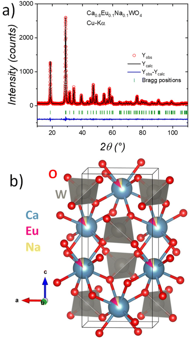 | ||
| Fig. 3 (a) Observed (red points), calculated (black full line) and difference (bottom) Rietveld profiles for Eu@CWO at room temperature. (b) Schematic view of the crystal structure of Eu@CWO. | ||
| ABO4 | Ca | Ca0.8Eu0.1Na0.1 | Ca0.8Gd0.1Na0.1 | Ca0.8Tb0.1Na0.1 |
|---|---|---|---|---|
| a (Å) | 5.2427(1) | 5.2497(2) | 5.2461(2) | 5.2464(2) |
| c (Å) | 11.3764(3) | 11.3841(5) | 11.3761(5) | 11.3720(5) |
| V (Å3) | 312.68(1) | 313.74(2) | 313.09(2) | 313.01(2) |
| A (8d) 0,1/4,5/8 | ||||
| Occ (Ca/Ln) | 1 | 0.828(4)/0.084(4) | 0.764(4)/0.116(4) | 0.832(4)/0.084(5) |
| U iso (Å2) | 0.010(1) | 0.010(2) | 0.013(2) | 0.008(2) |
| W (8c) 0,1/4,1/8 | ||||
| Occ | 1 | 1 | 1 | 1 |
| U iso (Å2) | 0.0080(4) | 0.0093(5) | 0.0093(6) | 0.0099(5) |
| O (16f) x,y,z | ||||
| X | 0.754(1) | 0.762(2) | 0.761(2) | 0.765(2) |
| Y | 0.400(1) | 0.398(2) | 0.398(2) | 0.400(2) |
| Z | 0.0414(6) | 0.041(1) | 0.041(1) | 0.040(1) |
| U iso (Å2) | 0.018(3) | 0.021(4) | 0.018(4) | 0.023(4) |
| Occ | 1 | 1 | 1 | 1 |
| Reliability factors | ||||
| R p, Rwp, χ2, RBragg | 5.5%, 7.8%, 0.6, 1.3% | 5.3%, 7.2%, 0.5, 1.2% | 5.3%, 7.2%, 0.6, 1.2% | 5.3%, 7.2%, 0.6, 1.3% |
The structural impact of Ln3+/Na+ co-doping on the unit-cell volume is plotted in Fig. 4a as a 3D ternary graph. As can be seen, the doped phases present a higher volume than the pristine phase (312.68 Å3) in agreement with the variation between Ca2+ and Ln3+/Na+ ionic radii (rCa2+ = 1.12 Å, rNa+ = 1.18 Å, rEu3+ = 1.07 Å, rGd3+ = 1.05 Å and rTb3+ = 1.04 Å).42 In addition, the increases in ionic size, from Tb3+ to Eu3+, included in the phases with two and three lanthanides, are observed in terms of the volume variations as revealed in the ternary graph (see Fig. 4a).
 | ||
| Fig. 4 (a) Unit-cell volume for different doped phases. The unit-cell volume for the pristine phase is 312.68(1) Å3. (b) Crystallite size for different doped phases. The crystallite size for the pristine phase is 27 nm. (c) Crystallite shape obtained for CaWO4 from SPH formalism. | ||
On the other hand, the diffraction peaks in all patterns present non-negligible broadening consistent with reduced crystallite sizes. Initial refinements were made considering isotropic size and strain effects yielding a proper fit in all phases; however, closer inspection reveals that several lines are not properly modelled showing a line of anisotropic broadening. This suggested that using a model of crystallite size (or strain) can enhance the pattern fitting; thus, after several tests the use of anisotropic crystallite size with spherical harmonics (SPH) treatment leads to a considerable improvement in the fitting. In the refinement of the SPH formalism, eight additional parameters were fitted according to the 4/m Laue class. Fig. S5† compares the results of the refinements using both isotropic and anisotropic models for the Eu3+-doped phase as representative of the series.
The main microstructural results, apparent size and strain, are listed in Table S2.† The average size is plotted in Fig. 4b where the effect after Ln3+/Na+ doping can be observed, while the phases doped with Gd3+ present lower average sizes than the other phases (Eu3+, Tb3+ and Eu3+/Tb3+) with respect to the pristine phase, which present a larger size. The size anisotropy was obtained for each sample, and that for CaWO4 is shown in Fig. 4c. For this pristine phase, the crystallite is slightly shorter in the [001] direction than in the [100] (or [010]) direction. To visualize differences between the obtained crystallite sizes, Table S2† lists the diameters in the [001], [100], [110] and [111] directions and Fig. 4c shows a schematic view of the crystallite shape for CWO. Despite the anisotropy being subtle, this behaviour (short along the [001] direction) is also observed in Gd3+-doped phases. In contrast, the phases without Gd3+ present the contrary deformation exhibiting a superior size along the [001] direction than that along the [100] direction. Therefore, a particular effect in the size (apparent and anisotropic) is observed for which there is no explanation. The unique difference found for Gd3+ with respect to Eu3+ and Tb3+ lies in its electronic configuration since Gd3+ presents half-filled 4f7 orbitals.
Solid state photoluminescence (SSPL)
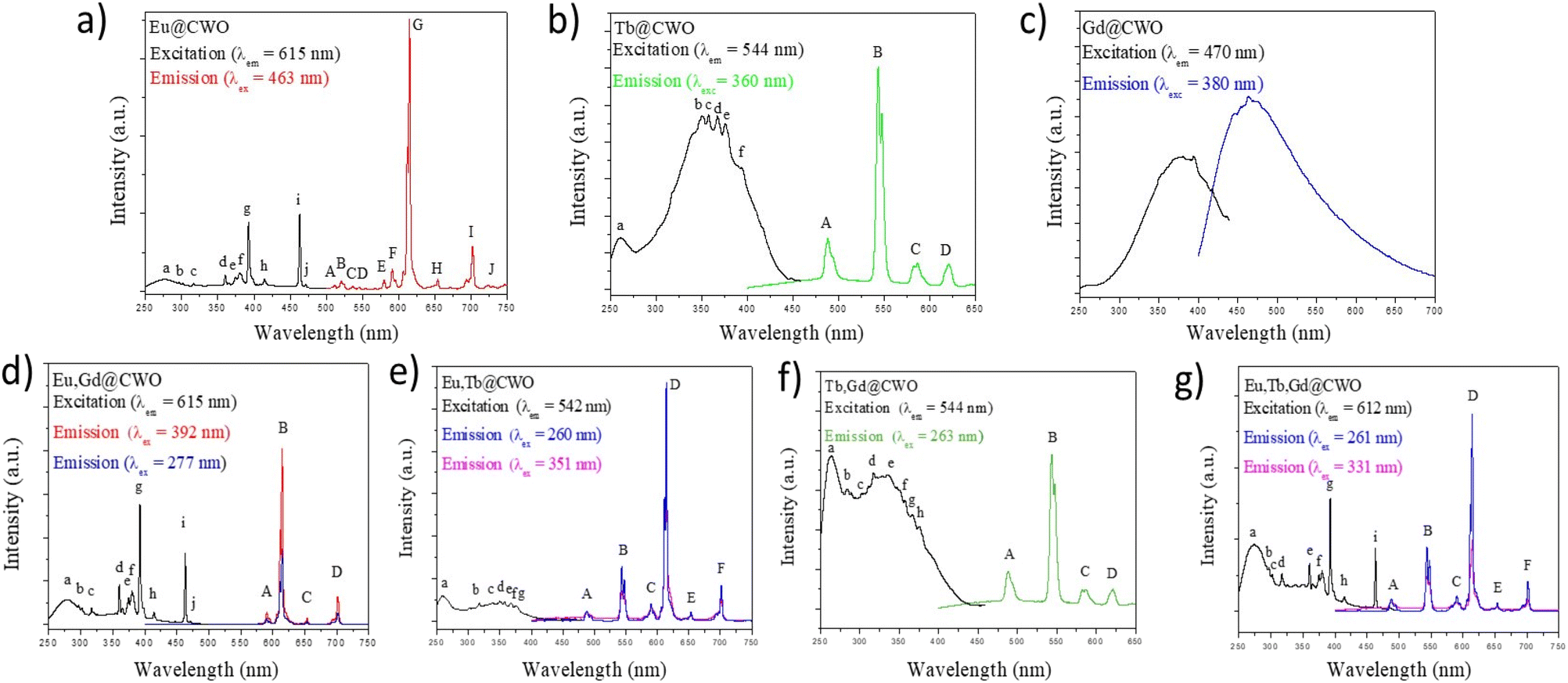 | ||
| Fig. 5 (a) Excitation (λem = 615 nm) (left) and emission (λex = 463 nm) (right) spectra of Eu@CWO. (b) Excitation (λem = 544 nm) (left) and emission (λex = 360 nm) (right) spectra of Tb@CWO. (c) Excitation (λem = 470 nm) (left) and emission (λex = 380 nm) (right) spectra of Gd@CWO. (d) Excitation (λem = 615 nm) (left) and emission (λex = 277 nm and λex = 393 nm) (right) spectra of Eu,Gd@CWO. (e) Excitation (λem = 542 nm) (left) and emission (λex = 260 nm and λex = 350 nm) (right) spectra of Eu,Tb@CWO. (f) Excitation (λem = 544 nm) (left) and emission (λex = 263 nm) (right) spectra of Tb,Gd@CWO. (g) Excitation (λem = 612 nm) (left) and emission (λex = 260 and 330 nm) (right) spectra of Eu,Tb,Gd@CWO. | ||
 | ||
| Fig. 6 (a) Powder samples under UV lamp illumination. (b) CIE diagram showing the colour performance of the studied compounds. | ||
The excitation spectrum of Tb@CWO was recorded in the 250–450 nm range, monitoring the 5D4 → 7F5 emission at 544 nm (Fig. 5b). The narrow peaks labelled a–f in the excitation spectrum correspond to transitions within the 4f shell of the Tb3+ ion. Under direct excitation into the 4f levels (5G5 ← 7F6, 360 nm), the typically narrow peaks of Tb3+ are observed, yielding green emission. The corresponding assignments of the excitation 2S+1LJ ← 7F6 and the emission 5D4 → 7F6, 5D4 → 7F5, 5D4 → 7F4 and 5D4 → 7F3 electronic transitions are shown in Fig. 5b. The most intense emission peak located at 544 nm shows a mono-exponential decay profile (Fig. S7b†) with a τobs value of 1.05 ms. In comparison with the Tb@CaWO4 nanowires obtained by Lin and colleagues, the τobs value of Tb@CWO increased by 28%.43
In the case of Gd@CWO, a broad band located at 470 nm is observed when the sample is excited at 380 nm (see Fig. 5c). This doped phase does not exhibit any sharp lines from the 4f shell of the Gd3+ ion, neither in the excitation nor in the emission spectrum. This fact is expected since the emissive level corresponding to the 6P7/2 state of the Gd3+ ion lies at too high an energy level to be populated by most antenna systems.1,6 Consequently, the excitation and emission spectra from Gd-doped samples are quite similar to those of the host matrix.
First, the excitation spectrum of Eu,Gd@CWO shows a broad band located at 277 nm accompanied by more intense peaks related to Eu3+ ions. From the set of peaks, the most intense is located at 393 nm and is ascribed to the 5L6 ← 7F1 transition. Two excitation experiments when λexc = 277 nm and 393 nm were carried out to find a feasible way to create the most intense emission spectrum. Direct lanthanide sensitization seems to be an efficient pathway to yield emission with intense peaks ascribed to the 5D0 → 7FJ (J = 0–4) transitions (see Fig. 5d). Also, the excitation spectrum of Eu,Tb@CWO exhibited a broad band accompanied by peaks belonging to Eu3+ and Tb3+ ions, as shown in Table S3.† By excitation from the host material (260 nm), or by selecting the maximum excitation peak from the lanthanide (350 nm, 5D4 ← 7F0 (Eu3+) transition), a typical Eu3+ emission is seen, which is accompanied by some peaks from Tb3+ ions (Fig. 5e). Due to the emissive level of Tb3+ (20492 cm−1) being higher than that from Eu3+ (17271 cm−1), it is feasibly attributed to a metal-to-metal charge transfer (MMCT) Tb → Eu, with consequent increments in the emission parameters (see Table 2). This phenomenon has been successfully explained in Tb3+/Eu3+@Sc2(WO4)3 compounds.44
| Eu-based material | I tot/IMD | 1/τr | τ r/ms | k r/s−1 | k exp/s−1 | k nrad/s−1 | τ obs/ms | QYEu% |
|---|---|---|---|---|---|---|---|---|
| Eu@CWO | 16.53 | 817.6 | 1.22 | 817.6 | 943.4 | 125.8 | 1.06 | 86.7 |
| Eu,Gd@CWO | 15.14 | 749.0 | 1.30 | 748.9 | 1043 | 293.8 | 0.959 | 71.8 |
| Eu,Tb@CWO | 14.90 | 737.1 | 1.35 | 737 | 751.9 | 14.83 | 1.33 | 98 |
| Eu,Tb,Gd@CWO | 13.90 | 687.4 | 1.45 | 687.4 | 900.9 | 213.5 | 1.11 | 76 |
By monitoring the excitation spectrum of Tb,Gd@CWO at an emission centred at 544 nm, the most intense signal corresponded to the CWO matrix with respect to the peaks 2S+1LJ ← 7F6 from Tb3+ ions (Fig. 5g). Then, this wavelength was selected for excitation. Upon host matrix sensitization (λexc = 263 nm), Tb,Gd@CWO exhibits four intense 5D4 → 7Fn emission transitions (Fig. 5f and Table S3†). The most intense emission peak, 5D4 → 7F5, is responsible for its green emission at 544 nm. Its mono-exponential decay profile (Fig. S7e†) shows a τobs value of 0.76 ms.
This behaviour is also reflected when the τobs values are analysed. The obtained lifetime from Eu,Gd@CWO is slightly smaller than that from Eu@CWO with values of 0.96 and 1.08 ms (see Fig. S5a and S5d†). Similarly, when τobs values of both Tb,Gd@CWO and Tb@CWO are compared, the co-doped sample exhibited a lifetime of 0.76 ms while the Tb-doped sample showed a value of 1.05 ms (see Fig. S5b and S5e†). Besides, the same effect could be seen in Eu,Tb@CWO in comparison with Eu,Tb,Gd@CWO, exhibiting a decrease of Eu3+ emission from 1.33 to 1.11 ms (see Fig. S5c and S5f†), but accompanied by a slight increment of τobs for Tb3+ from 0.52 to 0.61 ms. All these results reinforce the quencher-role of Gd3+ ions in the set of compounds reported herein.
From the lifetime measurements, all the decay processes were successfully fitted using a mono-exponential equation (eqn (1)):
 | (1) |
This model suggests the presence of one emitting centre in the structure. This behaviour can be related to the crystallographic features where each doped Ln3+ is edge-connected to four AO8 polyhedra. Considering these features, the Rietveld analysis revealed that the lanthanides occupy 10% of the Ca2+ sites. It is possible to assume that the different lanthanide environments do not affect the emitting performance.
To qualify the ability of the host matrix to sensitize the emission of Eu3+ centres, and to acquire information on the relationship between the structure and photoluminescence properties, the photophysical parameters of the Eu-doped samples were analysed.
For a suitable analysis of the photoluminescence efficiency of the Eu-doped samples, the intrinsic europium quantum yield, QYEu, was calculated. This parameter expresses how well the radiative processes compete with the non-radiative pathways and indicates the optimized quantum efficiencies for these materials. Assuming that non-radiative (knr) and radiative (kr) processes are essentially involved in the depopulation of the 5D0 state, QYEu can be expressed as:
| QYEu = kr/(kr + knrad) | (2) |
Generally, non-radiative contributions, knrad, include back-energy transfer to the sensitizer, electron transfer quenching, lanthanide self-quenching and quenching by matrix vibrations.45 The radiative contribution kr can be calculated from the equation:
| kr = 1/τr | (3) |
The so-called radiative lifetime τrad can be approximated for Eu(III) using eqn (4):46
| krad = (1/τrad) = AMD,0·n3·(Itot/IMD) | (4) |
In eqn (4), AMD,0 is the spontaneous emission probability of the 5D0 → 7F1 magnetic dipole transition equal to 14.65 s−1, n is the refractive index (1.5), Itot is the total integrated emission of the 5D0 → 7FJ (J = 0–6) transitions and IMD is the integrated emission of the 5D0 → 7F1 magnetic dipole transition. Besides, if τrad is known, QYEu can be calculated using the τobs value. Based on eqn (1) and (4), QYEu can be calculated as:
| QYEu = τobs/τrad | (5) |
At the same time, knowledge of both τobs and τrad enables the determination of the overall rate of non-radiative deactivation. Hence, the τrad value is an important parameter in the photophysical description of lanthanide luminescence. The photoluminescence parameters of Eu@CWO, Eu,Gd@CWO, Eu,Tb@CWO and Eu,Tb,Gd@CWO are summarized in Table 2.
As can be seen in Table 2, the influence of the gadolinium ions on the PL properties of doped samples disagrees with the regular performance as an enhancer of luminescence. The kr value of Eu@CWO, is higher than that of the corresponding co-doped samples. Nevertheless, when Tb3+ is added, it promotes a decrease in the knrad value related to the energy migration mechanism from Tb → Eu (see Fig. 7). This fact is reinforced when τobs and QYEu demonstrated higher values from the set of samples (Table 2). Moreover, all the τobs values for europium reported here (Table 2) are higher than those from analogous CaWO4-doped compounds, making them interesting materials for long-term red illumination applications.32,47
 | ||
| Fig. 7 Energy diagram of the Ln@CWO compounds studied herein. | ||
Besides, we have demonstrated the effect of a decrease of concentration quenching by incorporating Gd3+ as a doping ion and further improving emission of 2D-coordination polymers based on carboxylates and lanthanides (Eu and Sm).48 Also, Kaczmarek et al.49 reported the improvement in the luminescence properties in a series of co-doped Ln@Y2WO6 (Ln: Sm, Eu, Dy) by adding Gd3+ ions. However, there are few investigations regarding the quenching effect by adding Gd3+ as a doping ion. Meza et al. reported quenching effects in Eu3+@Gd2O3 samples, which are attributable to back energy transfer to Eu → O2−.50 Besides, Nosov et al. have reported the decrease in both emission intensities and lifetime values (up to 7%) of Sm3+ emission (5G5/2 → 6H7/2) due to the incorporation of Gd3+ as co-dopant in a family of NaY0.98−xSm0.02LnxF4 (Ln = Gd, Lu, La) compounds.51 The authors explain this fact in terms of a distortion in the local geometry of the emissive ions due to the presence of Gd3+, yielding an increase in knrad. Moreover, high-quality light performance requires obtaining the Commission International de l'Eclairage (CIE) x,y coordinates, with correlated colour temperature (CCT) parameters for lighting applications. The quantification of colour emission of different luminescent materials allows their comparison by studying the corresponding light-emitting performance. In this sense, the colour coordinates are usually calculated using the CIE x,y chromaticity system and plotted in a two-dimensional diagram. The colour emission of all the compounds was quantified as displayed in Fig. 6. Also, all the samples showed CCT values between 1800 and 7800 K, respectively (see Table 3), matching the human eye-friendly application range.
| Material | CIE x | CIE y | Colour | CCT (K) |
|---|---|---|---|---|
| Eu@CWO | 0.616 | 0.377 | Reddish orange | 1836.4 |
| Tb@CWO | 0.298 | 0.51 | Yellowish green | 6271.9 |
| Eu,Tb@CWO | 0.565 | 0.409 | Orange | 1782.3 |
| Eu,Gd@CWO | 0.656 | 0.343 | Reddish orange | 2854.1 |
| Tb,Gd@CWO | 0.321 | 0.591 | Yellowish green | 5703 |
| Eu,Tb,Gd@CWO | 0.535 | 0.429 | Yellowish orange | 2049.5 |
| CWO | 0.289 | 0.334 | Blue | 7833.2 |
Finally, as a “proof of concept” for the design and fabrication of devices, Eu@CWO, Eu,Gd@CWO, Eu,Tb@CWO and Eu,Tb,Gd@CWO were selected and deposited onto glass substrates using a spin-coating technique.
Spin coating is a thin-film coating technique using a flat substrate (e.g. gold, copper, glass) applying a film with thickness at the nano- or microscale. The functional thin films are coated on glass or single-crystal substrates. To fabricate oxide layers, the precursors are usually prepared through the “sol–gel” route, and after spin coating, the substrates are heated at high temperature to obtain the oxide layer.52 Homogeneity and uniformity are critical properties of thin films for device implementations for technological applications that require a reproducible and confident response, such as photocatalysis, sensing and visible light emitters.53
After several experiments, the most optimal variables for film design with these materials were 2000 rpm, 1 min per step, with a volume of 0.25 mL of 20 mg mL−1 concentration added onto the glass substrate, resulting in films with the best homogeneity and coverage.
As can be seen in Fig. 8, homogeneously uniform and flat films are obtained with a measured cross-section of 147 μm. A retro-dispersed electron micrograph (Fig. 8f) can also give information regarding the uniformity and the absence of surface defects. Besides, under UV illumination, the films conserve luminescence as if in powder form (see insets in Fig. 9), which is desirable for exploring potential sensing applications for small molecules.
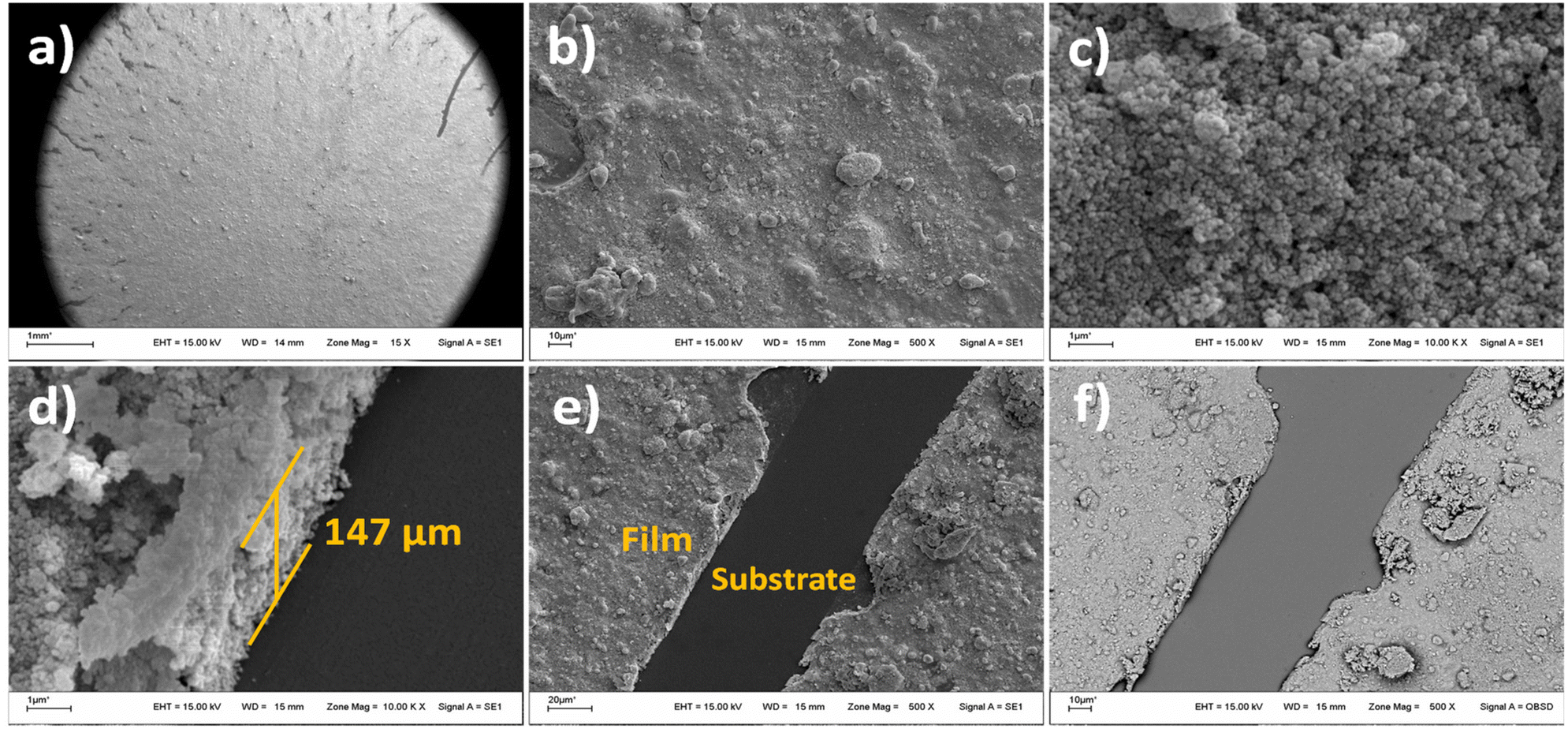 | ||
| Fig. 8 SEM images of film I observed at 15× (a), 500× (b) and 1000× (c and d) magnification. (e) Micrograph of the thin film observed at 500× magnification. (f) Retro-dispersed electron image. | ||
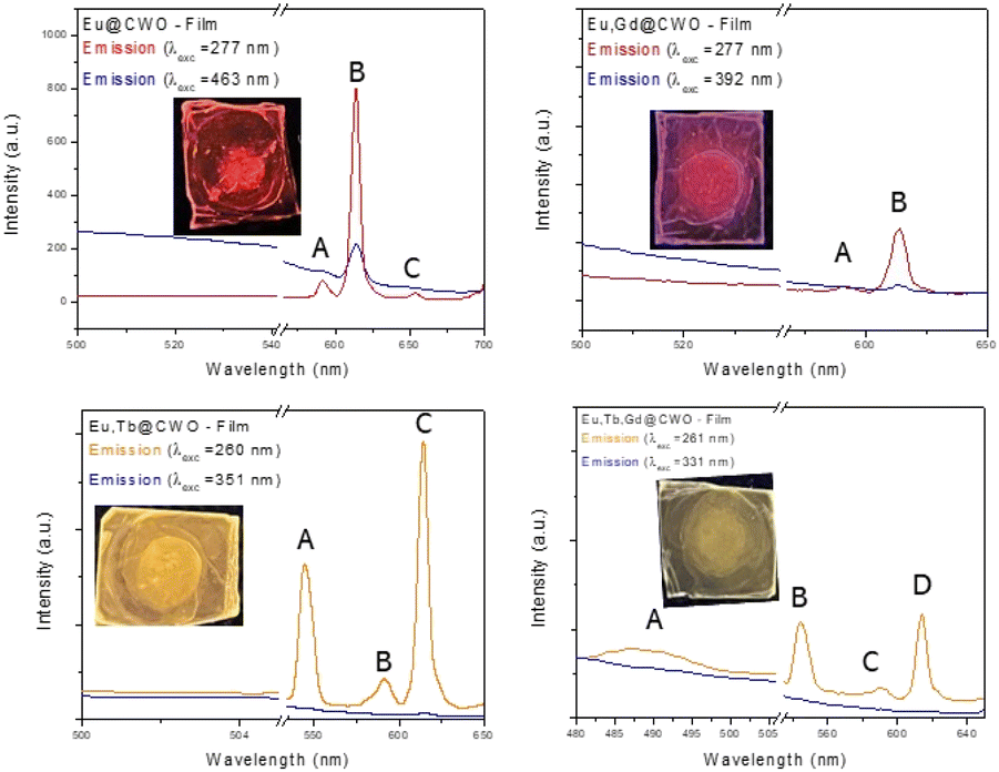 | ||
| Fig. 9 PL spectra of the films upon excitation with light of two different wavelengths and photographs (insets) of the thin films upon UV irradiation. | ||
Finally in order to analyse the red-emission performance of Eu-based films, steady-state luminescence measurements were performed. As can be seen in Fig. 9, there is a particular sensitization of lanthanide emission, through matrix excitation. A direct lanthanide excitation seems not the best choice to enhance the radiative pathways as the intensities in the emission spectra are relatively much lower. The absorption of the biologically active states Pfr and Pr in plants is also shown in Fig. 10 for comparison with the 5D0 → 7F2 transition signal. A significant overlap can be found, indicating that Eu3+ emission in both powder or thin films can be utilized as light for plant growth.
 | ||
| Fig. 10 PL emission spectra of Eu@CWO and Eu,Tb@CWO in addition to the absorption of biologically active states Pr and Pfr in plants. | ||
Conclusions
A set of phases with formula Ca1−2xLnxNaxWO4 (x = 0 and 0.1; Ln = Eu, Tb and Gd) (namely Eu@CWO, Tb@CWO and Gd@CWO) and co-doped phases with LnxLn′y = Eu0.05Tb0.05, Eu0.05Gd0.05, Tb0.05Gd0.05 (Eu,Tb@CWO, Eu,Gd@CWO and Tb,Gd@CWO) and Eu0.033Tb0.033Gd0.033 (Eu,Tb,Gd@CWO) was successfully synthesized using a sol–gel method followed by calcination at mild temperatures yielding micro-structures of around 10–200 μm. Besides, an in-depth structural and microstructural analysis was carried out by employing powder X-ray diffraction accompanied by Rietveld refinements. This study is remarkable for its novelty in covering wolframate-type compounds that are not commonly reported, which is important for designing micro- and nanomaterials. Moreover, the solid-state photoluminescence (SSPL) in the visible region was analysed by recording the excitation and emission spectra and calculating the lifetimes from the decay profiles. Besides, the intrinsic europium quantum yields (QYs), radiative and non-radiative constants and CIE colour coordinates were calculated and related to the energy transfer processes between lanthanides and the host matrix. The QYs fall into the 76–98% range with the highest value obtained being that for the Eu,Tb@CWO sample. This result demonstrates an efficient energy transfer from Tb3+ to Eu3+ to yield visible photoluminescence accompanied by the longest τobs value in the set (1.33 μs). Finally, the europium-based compound was selected for thin-film fabrication by an immobilizing spin-coating method and by controlling several experimental parameters, a homogeneous thin-film coating with ross-section of 150 μm on a glass substrate was yielded. These results indicate that Eu-containing CWO materials have potential for application in indoor plant cultivation LED devices and solid-state visible-light emitters with variety in their colour of luminescence.Data availability
The data supporting this article have been included as part of the ESI.†Conflicts of interest
There are no conflicts to declare.Acknowledgements
This work was supported by the Consejo Nacional de Investigaciones Científicas y Técnicas (CONICET), AGENCIA and Universidad Nacional de San Luis (projects: PIP 2972, PICT 20202-2437 and PROICO 02-2320). V. P. thanks the Ph.D. CONICET fellowship for the financial support. G. E. G., C. A. L. and G. E. N. are members of CIC-CONICET (Carrera del Investigador Científico). We also thank Lic. Esteban Crespo from INFAP-UNSL for his assistance in SEM measurements.References
- N. Yeh and J. Chung, Renewable Sustainable Energy Rev., 2009, 13, 2175–2180 CrossRef CAS.
- M. Olle and A. Viršile, Agric. Food Sci., 2013, 22, 223–234 CrossRef.
- K. Li and R. Van Den, Chem. Commun., 2019, 55, 10697–10700 RSC.
- W. Kang, J. Park, K. Park and J. Son, Hortic., Environ. Biotechnol., 2016, 57, 573–579 CrossRef.
- M. Sabzalian, P. Heydarizadeh, M. Zahedi, A. Boroomand, M. Agharokh, M. Sahba and B. Schoefs, Agron. Sustainable Dev., 2014, 34, 879–886 CrossRef.
- Y. Tsai, C. Chiang, W. Zhou, J. Lee, H. Sheu and R. Liu, J. Am. Chem. Soc., 2015, 137, 8936–8939 CrossRef CAS PubMed.
- C.-T. Chen, T.-J. Lin, M. S. Molokeev and W.-R. Liu, Dyes Pigm., 2018, 150, 121–129 CrossRef CAS.
- K. Li, M. Shang, H. Lian and J. Lin, J. Mater. Chem. C, 2016, 4, 5507–5530 RSC.
- T. Pulli, T. Dönsberg, T. Poikonen, F. Manoocheri, P. Kärhä and E. Ikonen, Light: Sci. Appl., 2015, 4, 332 CrossRef.
- Z. Zhou, J. Zheng, R. Shi, N. Zhang, J. Chen, R. Zhang, H. Suo, E. Goldys and C. Guo, ACS Appl. Mater. Interfaces, 2017, 9, 6177–6185 CrossRef CAS PubMed.
- G. D. Massa, H. Kim, R. M. Wheeler and C. A. Mitchell, HortScience, 2008, 43, 1951–1956 Search PubMed.
- H. Yu, J. Chan, B. Devakumar and X. Huang, Mater. Today Chem., 2023, 30, 101548 CrossRef.
- N. Ma, W. Li, B. Devakumar, Z. Zhang and X. Huang, Mater. Today Chem., 2021, 21, 100512 CrossRef CAS.
- K. Binnemans, Chem. Rev., 2009, 109, 4283–4374 CrossRef CAS PubMed.
- C. D. S. Brites, P. P. Lima, N. J. O. Silva, A. Millán, V. S. Amaral, F. Palacio and L. D. Carlos, New J. Chem., 2011, 35, 1177 RSC.
- L. D. Carlos, R. A. S. Ferreira, V. de Z. Bermudez and S. J. L. Ribeiro, Adv. Mater., 2009, 21, 509–534 CrossRef CAS PubMed.
- J.-C. G. Bünzli, S. Comby, A.-S. Chauvin and C. D. B. Vandevyver, J. Rare Earths, 2007, 25, 257–274 CrossRef.
- N. Ma, W. Li, B. Devakumar and X. Huang, Inorg. Chem., 2022, 61, 6898–6909 CrossRef CAS PubMed.
- X. Huang, J. Liang, S. Rtimi, B. Devakumar and Z. Zhang, Chem. Eng. J., 2021, 405, 126950 CrossRef CAS.
- S. Wang, Q. Sun, B. Devakumar, J. Liang, L. Sun and X. Huang, J. Alloys Compd., 2019, 804, 93–99 CrossRef CAS.
- E. G. Moore, A. P. S. Samuel and K. N. Raymond, Acc. Chem. Res., 2009, 42, 542–552 CrossRef CAS PubMed.
- J.-C. G. Bünzli, Chem. Rev., 2010, 110, 2729–2755 CrossRef PubMed.
- K. Zhenga and P. Ma, Dalton Trans., 2024, 53, 3949–3958 RSC.
- G. Xiang, Z. Liu, Z. Yang, Y. Wang, L. Yao, S. Jiang, X. Zhou, L. Li, X. Wang and J. Zhang, J. Mater. Chem. C, 2023, 11, 16310–16315 RSC.
- D. Yue, Q. Li, W. Lu, Q. Wang, M. Wang, C. Li, L. Jin, Y. Shi, Z. Wang and J. Hao, J. Mater. Chem. C, 2015, 3, 2865–2871 RSC.
- M. Lin, L. Xie, Z. Wang, B. S. Richards, G. Gao and J. Zhong, J. Mater. Chem. C, 2019, 7, 2971–2977 RSC.
- W. Bai, Y. Liu, Y. Wang, X. Qiang and L. Feng, Ceram. Int., 2015, 10, 12896–12900 CrossRef.
- (a) R. Saraf, C. Shivakumara, N. Dhananjaya, S. Behera and H. Nagabhushana, J. Mater. Sci., 2015, 50, 287–298 CrossRef CAS; (b) R. Z. Zhuang, L. Z. Zhang, Z. B. Lin and G. F. Wang, Mater. Res. Innovations, 2008, 12, 62–65 CrossRef CAS; (c) S. Belogurov, V. Kornoukhov, A. Annenkov and A. Borisevich, et al. , IEEE Trans. Nucl. Sci., 2015, 52, 1131–1135 CrossRef; (d) Z. Hou, R. Chai, M. Zhang, C. Zhang, P. Chong, Z. Xu, G. Li and J. Lin, Langmuir, 2009, 25, 12340–12348 Search PubMed.
- J. Liu, A. M. Kaczmarek, J. Billet, I. Van Driessche and R. Van Deun, Dalton Trans., 2016, 45, 12094–12102 RSC.
- J. Huang, Q. Li, J. Wang, L. Jin, B. Tian, C. Li, Y. Shi, Z. Wang and J. Hao, Dalton Trans., 2018, 47, 8611–8618 RSC.
- (a) Y. Xie, S. Ma, Y. Wang, M. Xu, C. Lu, L. Xiao and S. Deng, Opt. Mater., 2018, 77, 13–18 CrossRef CAS; (b) R. Saraf, C. Shivakumara, N. Dhananjaya, S. Behera and H. Nagabhushana, J. Mater. Sci., 2015, 50, 287–298 CrossRef CAS; (c) A. Xie, X. Yuan, S. Hai, J. Wang, F. Wang and L. Li, J. Phys. D: Appl. Phys., 2009, 42, 105107 CrossRef; (d) A. Khanna and P. S. Dutta, J. Solid State Chem., 2013, 198, 93–100 CrossRef CAS; (e) Z. H. Zhang, Q. Huang, X. Zhao and Z. L. Huang, Phys. Status Solidi, 2009, 2839–2843 CrossRef CAS; (f) J. Zhang, L. Li, W. Zi, N. Guo, L. Zou, S. Gan and G. Ji, J. Phys. Chem. Solids, 2014, 75, 878–887 CrossRef CAS; (g) C. Du, F. Lang, Y. Su and Z. Liu, J. Colloid Interface Sci., 2013, 394, 94–99 CrossRef CAS PubMed; (h) Z. Zhou, Y. Yu, X. Liu, W. Ye, G. Hu, B. Lei and Y. Yan, J. Adv. Ceram., 2015, 4, 318–325 CrossRef CAS.
- G. E. Gomez, C. A. López, R. L. Ayscue III, K. E. Knope, M. del R. Torres Deluigi and G. E. Narda, Dalton Trans., 2019, 48, 12080–12087 RSC.
- L. Yun, W. Shi-yu, L. Jin-yang and S. Xiao-lei, Chin. J. Lumin., 2014, 35, 1201–1204 CrossRef.
- Y. Ouyang, X. Zhang, J. Wang, X. Wang and X. He, Cailiao Daobao, 2016, 30, 33–37 Search PubMed.
- H. M. Noh, E. O. Kim, J. H. Jeong, K. R. Kang, Y. J. Kim, K. C. Lee, J. H. Lee, Y. D. Park and J. H. Kim, New Phys.: Sae Mulli, 2014, 64, 717–722 CAS.
- C. Li, C. Lin, X. Liu and J. Lin, J. Nanosci. Nanotechnol., 2008, 8, 1183–1190 CrossRef CAS.
- D. Athayde, D. F. Souza, A. Silva, D. Vasconcelos, E. H. Nunes, J. C. D. da Costa and W. Vasconcelos, Ceram. Int., 2016, 42, 6555–6571 CrossRef CAS.
- H. M. Rietveld, J. Appl. Crystallogr., 1969, 2, 65–71 CrossRef CAS.
- J. Rodríguez-Carvajal, Phys. B, 1993, 192, 55–69 CrossRef.
- P. Thompson, D. E. Cox and J. B. Hastings, J. Appl. Crystallogr., 1987, 20, 79–83 CrossRef CAS.
- R. M. Hazen, L. W. Finger and J. W. E. Mariathasan, J. Phys. Chem. Solids, 1985, 46, 253–263 CrossRef CAS.
- R. D. Shannon, Acta Crystallogr., Sect. A, 1976, 32, 751–767 CrossRef.
- Z. Hou, C. Li, J. Yang, H. Lian, P. Yang, R. Chai, Z. Cheng and J. Lin, J. Mater. Chem., 2009, 19, 2737 RSC.
- B. Fu, H. Yan, R. Li, Z. Liao, B. Qiu, G. Gong, H. Huang, Y. Sun, H. Wen and J. Liao, Dalton Trans., 2024, 53, 798–807 RSC.
- A. Beeby, I. M. Clarkson, R. S. Dickins, S. Faulkner, D. Parker, L. Royle, A. S. de Sousa, J. A. G. Williams and M. Woods, J. Chem. Soc., Perkin Trans. 2, 1999, 493–504 RSC.
- A. Chauvin, F. Gumy, D. Imbert and J. G. Bünzli, Spectrosc. Lett., 2004, 37(5), 517–532 CrossRef CAS.
- S. Bai, Y. Liu, G. Tan, W. Liu, D. Liu, R. Wang, Y. Zhu, S. Ye and H. Ren, J. Lumin., 2020, 225, 117351 CrossRef CAS.
- G. E. Gomez, M. C. Bernini, E. V. Brusau, G. E. Narda, D. Vega, A. M. Kaczmarek, R. Van Deun and M. Nazzarro, Dalton Trans., 2015, 44, 3417–3429 RSC.
- A. M. Kaczmarek, K. V. Hecke and R. Van Deun, Inorg. Chem., 2014, 53, 9498–9508 CrossRef CAS PubMed.
- O. Meza, E. G. V. Leal, L. A. Diaz-Torres, H. Desirena, J. L. Rodríguez-López and E. Pérez, J. Phys. Chem., 2014, 118(8), 1390–1396 CrossRef CAS PubMed.
- V. G. Nosov, A. A. Betina, T. S. Bulatova, P. B. Guseva, I. E. Kolesnikov, S. N. Orlov, M. S. Panov, M. N. Ryazantsev, N. A. Bogachev and M. Y. Skripkin, Materials, 2023, 16, 2157 CrossRef CAS PubMed.
- G. George, S. R. Ede and Z. Luo, Fundamentals of Perovskite Oxides: Synthesis, Structure, Properties and Applications, 1st edn, 2020 Search PubMed.
- S. Majumder, Nanostructured Materials for Visible Light Photocatalysis, Elsevier, 2022, pp. 47–113 Search PubMed.
Footnote |
| † Electronic supplementary information (ESI) available: Tables of Rietveld analysis, 4f–4f* transition assignments, decay profiles and fittings, host-matrix emission spectra and extra SEM micrographs. See DOI: https://doi.org/10.1039/d5dt00366k |
| This journal is © The Royal Society of Chemistry 2025 |