
 Open Access Article
 This Open Access Article is licensed under a
 Creative Commons Attribution 3.0 Unported Licence
Advances in resistive switching memory: comprehensive insights into ECM mechanisms through TEM observations and analysis
Woonbae
Sohn
a,
Hyerim
Kim
b,
Jung Hun
Lee
c,
Young-Seok
Shim
d,
Cheon Woo
Moon
*e and
Hyojung
Kim
 *f
*f
aMetropolitan Seoul Center, Korean Basic Science Institute, Seoul, 02855, Republic of Korea
bSchool of Advanced Materials Science and Engineering, Sungkyunkwan University, Suwon, 16419, Republic of Korea
cDepartment of Materials Science and Engineering and the Materials Research Center, Northwestern Universiy, Evanston, IL 60208, USA
dSchool of Energy, Materials and Chemical Engineering, Korea University of Technology and Education, Cheonan, 31253, Republic of Korea
eDepartment of Display Materials Engineering, Soonchunhyang University, Asan, 31538, Republic of Korea
fDepartment of Semiconductor Systems Engineering, Sejong University, Seoul, 05006, Republic of Korea. E-mail: hyojungkim0912@sejong.ac.kr
First published on 29th May 2025
Abstract
The information age requires improved devices, especially performance and output, due to data processing, power consumption, flexibility, multifunctionality, cost efficiency, and fabrication technologies. Examining resistive switching properties indicated that the conductive filament mechanism and the movement of ions from dielectric layers or electrodes play a crucial role in facilitating resistive switching. Despite extensive studies employing various materials to clarify the resistance switching in memory devices, the fundamental mechanisms still need to be more adequately understood. In ECM, metal cations move from a top electrode that shows electrochemical activity, creating conductive metal filaments. The complex nature of ion migration at the nanoscale and the associated redox reaction in resistive switching require a thorough understanding through transmission electron microscopy (TEM). In situ TEM enables the real-time observation of resistive switching dynamics, highlighting the limitations of static ex situ TEM. The observation of filament formation via TEM facilitates atomic-resolution investigations into the real-time evolution of nanostructures within resistive switching memory systems. Understanding resistive switching behavior may improve the performance and reliability of memory devices. This assessment can be gained from applying electrodes featuring resistive switching material systems for ECM, which aim to advance the development of universal nonvolatile memory devices.
 Woonbae Sohn | Woonbae Sohn received his PhD in 2018 from the Department of Materials Science and Engineering, Seoul National University. He is a postdoctoral researcher at the Korean Basic Science Institute. He was a research associate at the National University of Singapore from 2021 to 2022. He had worked at the Korea Institute of Ceramic Engineering and Technology. His research interest includes materials analysis using aberration-corrected STEM and EELS of 2D materials, oxide nanocatalysts, cathodes for lithium–ion batteries, and solid electrolytes. |
 Hyerim Kim | Hyerim Kim is currently a research associate at Kangwon National University. She received her PhD from the KU-KIST Graduate School of Converging Science and Technology at Korea University, where she studied on improving the electrical conductivity and oxidation resistance of MXenes through surface functionalization. Her expertise lies in the synthesis and modification of two-dimensional nanomaterials for electronic device applications. She focuses on developing high-performance materials for use in memory, energy, and sensor technologies. |
 Jung Hun Lee | Jung Hun Lee has been a postdoctoral researcher in the Department of Materials Science and Engineering at Northwestern University (NU), USA, since 2022. He received his PhD in Materials Science and Engineering from Seoul National University (SNU) in 2022, where he specialized in solution-process engineering for high-performance organic electronics. During his PhD, he also worked as a researcher at the Korea Institute of Industrial Technology (KITECH) for three years as part of his mandatory military service, focusing on wearable electronics for textile applications. His current research focuses on developing various two-dimensional (2D) materials for optoelectronic, magnetic, and quantum device applications. |
 Young-Seok Shim | Young-Seok Shim has been working as an Assistant Professor at the School of Energy, Materials & Chemical Engineering in the Korea University of Technology & Education (KOREATECH), Korea, since 2022. Before joining the KOREATECH, he was an Assistant Professor at Silla University (2020–2022). He received his PhD (2016) degree from the Department of Materials Science & Engineering at Yonsei University, Korea. From 2016 to 2017, he was a postdoctoral research associate at the Electronic Materials Center at the Korea Institute of Science & Technology (KIST). From 2018 to 2020, he joined the Department of Materials Science & Engineering at the Korea Advanced Institute of Science and Technology (KAIST) as a postdoctoral researcher. His research interests are micro/nanostructured materials and their large-area synthesis methods for gas sensing applications. He has published more than 60 international journal articles (SCI indexed). |
 Cheon Woo Moon | Cheon Woo Moon obtained his PhD degree from Seoul National University, Republic of Korea, in 2018. He worked as a researcher at the Ewha Womans University, Republic of Korea, from 2018 to 2022. Also, he worked as a postdoctoral researcher at the University of Nevada, Reno, the United States of America, at the Department of Chemistry from 2022 to 2023. Since 2023, he has been working at Soonchunhyang University in the Department of Display-Materials Engineering. His research mainly focuses on the connection of photonic materials to energy-related devices. Currently, active plasmonic devices include smart windows, smart pixels, sensors, and solar-to-fuel conversion. |
 Hyojung Kim | Hyojung Kim is an Assistant Professor in the Department of Semiconductor Systems Engineering at Sejong University, Seoul, South Korea. She received her PhD in Materials Science and Engineering from Seoul National University in 2021, where she focused on halide perovskite-based resistive switching memory. Her research encompasses next-generation non-volatile memory, in-memory computing systems, and lead-free electronic materials. She is particularly interested in the structural and chemical mechanisms governing ion migration and redox processes in emerging memory devices. |
1. Introduction
The era of information has heightened the need for advanced devices, particularly regarding their performance and production processes. This includes enhanced density, increased data processing capabilities, reduced power consumption, adaptability, multifunctionality, scalability, cost efficiency, and optimized fabrication processes.1–6 Considering the difficulties existing Si-based devices face in meeting these demands, there has been a focused initiative to discover active materials for future devices, particularly highlighting metal oxide semiconductors, organic semiconductors, and two-dimensional (2D) materials.7–13 Although electronic devices utilizing these technologies demonstrate impressive characteristics, there has consistently been a trade-off between their advantages and inherent limitations. Recent studies have increasingly shown that the microscopic mechanisms behind ECM-based resistive switching devices, especially ion migration and filament dynamics, offer substantial potential for new applications in neuromorphic computing, low-power logic circuits, and artificial intelligence hardware, thus connecting fundamental material insights with system-level functionality.Typically, the layers involved in resistive switching systems are composed of dielectric materials. The fundamental resistive switching processes mainly consist of ion movement originating from the dielectric layers or the electrodes.14,15 The mechanisms behind resistance switching in memory devices remain contentious, even with extensive studies on resistive switching memory utilizing various materials to clarify the observed changes in resistance.16–19 The conductive filament mechanism is recognized; however, notable discussions continue regarding essential elements such as the microscopic processes, composition, and morphology involved in producing and degrading conductive filaments. The filament primarily comprises ions that include oxygen vacancies, active metal cations, and anions.20,21 The fundamental concepts of resistive switching depend on the particular kind of ion migration within the dielectric material (e.g., HfO2, TiO2, Al2O3, etc.).22–24
The electrochemical metallization (ECM) mechanism shows the movement of cations from an electrode with electrochemical activity.25–27 Due to the reduction reaction occurring in a reducing environment, cations generate metal filaments that serve as a conductive pathway.
Since ion migration and the associated redox processes in resistive switching occur at the nanoscale level, transmission electron microscopy (TEM) is important in elucidating the characteristics and dynamic mechanisms involved. Unlike stationary observations of different resistance states in devices via traditional ex situ TEM, in situ TEM allows for real-time monitoring of dynamic processes during resistive switching. Observations from diverse material systems have uncovered indications of conducting filaments formed by metal atoms, including copper (Cu) and silver (Ag). The geometry and direction of growth or dissolution of these filaments are primarily influenced by the intricate kinetic parameters related to ion migration and redox reactions, leading to various modes of filament growth.28
This review explains the operational mechanism of the resistive switching memory device and provides a detailed description of the ECM. A detailed analysis of resistive switching behaviors is complemented by conventional ex situ TEM characterization of diverse resistance states, and in situ TEM further enables real-time visualization of the dynamic processes driving those switching behaviors.
2. Resistive switching memory device
2.1. Operating principles
Given the characteristics of the straightforward structure and benefits of data storage, resistive switching memory devices are considered a promising option for next-generation memory devices.29–33 The resistive switching memory device represents a prevalent category of two-terminal, metal–insulator–metal (MIM) devices, especially in the oxide-based device field.34 The memory elements comprise the top and bottom electrodes, with an insulating switching layer between them. The top electrode in the MIM stack is subjected to an external bias and is influenced by the applied voltage or current.35,36 The top electrodes are formed by directly depositing metallic materials onto the resistive switching layer. A different electrode, an electrically connected element, is called the bottom electrode. The device functions through a reversible and gradual decomposition of an insulating material.Applying appropriate voltage pulses to a device transitions it from a high resistance state (HRS) to a low resistance state (LRS), referred to as “electroforming.”37–40 Utilizing devices that skip the formation process is essential to reducing the impacts of high voltage stress during the initial operation stage. After the electroforming step, the LRS shifts to an HRS when a RESET voltage of opposite polarity is applied. This change is frequently called the “RESET process.”41–43 Following that, the change from an HRS to an LRS happens at the VSET, differing from the RESET process. Understanding the principles of resistive switching requires going through the SET and RESET procedures. Switching from SET to RESET indicates the ‘ON’ state, whereas the reverse transition corresponds to the ‘OFF’ state.44–46 Current compliance (CC) is a standard safeguard that limits current during the SET process.20,47,48
To ensure the reliability of the resistive switching device, a vital memory window (ON/OFF ratio), in addition to endurance and retention, needs to be achieved. Endurance quantifies the cycles required for reliable transitions from the ON and OFF.49–53 An increased endurance indicates the enhanced ability to handle repetitive programming-related tasks. Retention plays an important part in memory technology, as it determines the duration for which the recorded data remain accessible before it becomes inaccessible.54–56 The duration of data storage is deeply linked to energy efficiency, an important consideration given the growing volume of data. Moreover, the ON/OFF ratio plays a pivotal role in defining the memory window of a device.57,58 This significantly influences the probability of operational errors during the programming of the memristor. Consequently, optimizing the ON/OFF ratio is necessary to guarantee dependable storage functionality.
2.2. Bipolar and unipolar resistance switching modes
Fig. 1a presents a hysteresis loop of I–V observed during a sweep bipolar resistive switching mode.59 A notable rise in current was observed as the swept voltage changed from 0 V to threshold voltage (Vth), and an abrupt rise in electrical current triggered the shift from the HRS to the LRS.59–62 After that, the OFF state is attainable only when the film is reverted to a voltage of 0 V. Applying a negative bias leads to a rapid rise in the device's resistance upon reaching negative Vth, prompting a transition back to the HRS. The preference for unipolar switching behavior stems from its easy facilitation of read–write activities. Unipolar switching uses a consistent biased direction to activate and deactivate the process. Fig. 1b demonstrates the features of unipolar resistive switching behavior.59 Unlike bipolar resistive switching, unipolar resistive switching conducts both the SET and RESET events under the same voltage polarity.59,63,64 This process occurs under positive and negative voltage conditions, in which a small current flow characterizes the initial OFF state. The device activates the SET once the Vth attains a significant level, and typically, the Vth is more significant than bipolar resistive switching. Upon exceeding the Vth, the device will enter a deactivated state related to the same ON and OFF that occurs with reverse voltage. A high voltage bias can directly convert pristine resistive switching to the LRS, resulting in an inverted procedure. | ||
| Fig. 1 (a) Unipolar Switching mode of the resistive switching memory devices. (b) Bipolar Switching mode of the resistive switching memory devices. Reproduced with permission from ref. 59. Copyright 2013, Springer. (c) The ECM process of the resistive switching memory devices. Reproduced with permission from ref. 70. Copyright 2019, American Chemical Society. | ||
2.3. ECM process
The ECM phenomenon is frequently utilized to clarify the fundamental principles of devices that incorporate active metal electrodes with relatively high mobility, including silver (Ag), copper (Cu), nickel (Ni), and others.65–69 The interaction of active metals with switching layers depends on their Gibbs energy and oxidation rate.Fig. 1c illustrates ECM-type memory devices, showing the resistive switching phenomenon.70 Han et al. fabricated resistive switching memory devices utilizing halide perovskite comprising Ag top electrodes/CsSnI3/Pt, demonstrating the ECM process.
The observed resistive switching behavior is linked to the formation and rupture of conducting filaments within the switching layer, occurring during the SET and RESET operations. The resistive switching phenomenon observed in the ECM process is mainly attributed to the travel of metal cations from the active electrode.71 The Ag electrode undergoes dissolution through oxidation when a positive voltage is applied to it within an electric field characterized by a positive bias on the Ag electrode and a grounded Pt electrode. The external electric field drives the Ag cations within the perovskite layer towards the Pt electrode. Ag cation reduction occurs as they engage in ion hopping and arrive at the Pt electrode. The growth of an Ag metal nucleus occurs when the supersaturation level of the Ag cation is exceeded, leading to the creation of a metal filament that links the Pt and Ag electrodes. Applying an electric field in the reverse direction causes the filament to break down due to disintegration driven by Joule heating.34,40
From the description provided regarding filament development, various elements have been recognized as possible influences. The factors to consider are
(1) the presence of cation elements from the active electrode,
(2) the transport of the cation within the halide perovskite switching layer, and
(3) the accumulation of cations on the counter electrode.
ECM-based memory devices can operate at low voltages and currents while showing impressive ON/OFF ratios.66,72–74 Nonetheless, maintaining the resistance state after withdrawing the electric field presents a challenge.
2.4. Description of the formation of conducting filaments in an ECM-based memory device
Cylindrical conductive filaments develop within the resistive switching layer during formation or SET. Roy et al. utilized the phase field model to investigate the morphological evolution of conducting filaments driven by an electric field at a continuum scale.75 The simulation of active electrode dissolution involves analyzing the release of cations into the resistive switching layer, considering the incoming flux of cations from the active electrode. The established cation supersaturation, along with the implementation of the electric field, supplies the essential chemical and electrical driving forces required for the formation of conducting filaments. To comprehend the impact of higher dimensions on simulation outcomes, the filament formation processes for 2D and 3D systems are analyzed in Fig. 2a. The initial conducting filaments radius was established at 2.0 nm during the simulation. The voltage sweeping rate was set at a constant value of 0.01 V s−1. The dominant point effect of diffusion in the 3D simulation domain results in a voltage difference of 0.02 V compared to the 2D simulation for the forming current. Nonetheless, the morphology and trend in the I–V curves exhibit similarities. At this stage, the nucleation theory for forming the initial filament nucleus was neglected. This absence is attributed to various unknown factors, including the nucleation energy barrier, the rate of nucleation, and the surface tension terms arising from the interfaces between the bottom electrode/conducting filaments, bottom electrode/resistive switching layer, and switching layer/conducting filaments during the early phases of simulation. In Fig. 2b, the broken filament configurations were evaluated. The distance between the broken filaments is established at 2 nm. The filament contacts the broken end before reaching the counter electrode, which explains the nearly constant SET voltage. Nonetheless, as the gap between the broken ends of the filament increases, the relationship between the SET voltage and layer thickness exhibits variation. Therefore, the structure of the conducting filament influences the formation and SET voltages, potentially altering the device's performance. | ||
| Fig. 2 (a) Conducting filaments in 3D and 2D simulation domains. A voltage sweep of 0.01 V s−1 has been applied, acquiring the corresponding I–V curves. (b) Conducting filaments while applying voltage sweeping at a rate of 0.01 V s−1, along with the associated I–V characteristics during the forming and SET processes. Reproduced with permission from ref. 75. Copyright 2020, AIP Publishing. (c) Filament growth when the ion mobility and the redox rates are high. (d) In situ TEM observation of filament growth when ion mobility and the redox rates are low. (e) In situ TEM images when ion mobility is low, and the redox rates are high. (f) Observation of conducting filament growth when the ion mobility is high while the redox rates are low. Reproduced with permission from ref. 76. Copyright 2018, Elsevier. | ||
The dynamics influenced by external fields can provide deeper insights into the formation of filaments across various material systems. At times, the primary driving factor is the electrostatic potential gradient, and typically, there are four modes of filament growth when considering specific kinetic factors. With elevated ion mobilities and redox rates, positively charged metal ions are anticipated to quickly reach the inert electrode, where they will react, initiating filament growth from the inert electrode. The elevated redox rates ensure sufficient ion supply, resulting in a filament that takes on an inverted cone shape in Fig. 2c.76 Conversely, when the ion mobilities and the redox rates are low, nucleation of the ions occurs within the dielectric, and the subsequent evolution of filaments follows a process, ultimately resulting in fully formed conducting filaments, as depicted in Fig. 2d. In this case, the filament geometry manifests as a forward cone consisting of discrete metal clusters instead of a continuous metal wire. When the ion mobilities are low and redox rates are high, nucleation of the filament occurs within the dielectric, allowing for significant accumulation of the metal on the cathode sides of the nuclei. After the gaps between the sources of ions and the nuclei are filled, additional ionization and nucleation processes can occur, with the incomplete filament functioning effectively as part of the electrode, as illustrated in Fig. 2e. Nucleation occurs at the inert electrode when the ion mobilities are elevated and the redox rates are decreased. However, the supply of ions is insufficient, resulting in ion reduction mainly at the edges of the filaments due to elevated field strengths. This phenomenon drives branched filament growth toward the active electrode, as illustrated in Fig. 2f. Furthermore, the metal filament has the potential to extend into the inert electrode, which serves as a cation source that can lead to RESET failure. Introducing a barrier layer, such as graphene, at the interface between the resistive switching layer and the inert electrode has effectively prevented the diffusion of active metal ions or atoms.
2.5. ECM-based resistive switching memory device
As stated, one electrode in an ECM-based memory device must exhibit electrochemical activity. This section introduces resistive switching memory devices grounded in ECM, emphasizing the classification based on the top electrodes. The wide use of an Ag top electrode in the electrochemical metallization process is frequently observed in memory devices.32,34 Kim et al. investigated a halide perovskite flexible memory array that exhibits strong reliability (Fig. 3a).77 The resistive switching memory devices exhibited filamentary and bipolar characteristics due to the Ag conducting filament. The Ag and Pt metals were the top and bottom electrodes, respectively. The resistive switching characteristics of the Ag/halide perovskites/Pt memory device are illustrated in Fig. 3b. A direct current (DC) voltage sweep was conducted to evaluate the I–V characteristics. To prevent breakdown due to high current, the CC was set at 1 mA. The device exhibited a low current of 10−11 A during its initial state. The bipolar resistive switching behavior was observed to occur abruptly and reliably at +0.15 V and −0.15 V, exhibiting a significant ON/OFF ratio. Notably, reversible resistive switching characteristics can be attained with a significant ON/OFF ratio (107) while employing an ultralow electric field of 5 × 10³ V cm−1. Endurance and retention were evaluated by subjecting the devices to alternating current (AC) voltage pulses to assess their reversible and reliable resistive switching behaviors. The endurance cycles illustrated in Fig. 3c functioned over 5 × 10⁶ times, exhibiting a substantial ON/OFF ratio exceeding 107. However, performance began to decline after 107 cycles, with programming at +2 V for 100 μs, erasing at −3 V for 100 μs, and a reading process at +0.05 V. Furthermore, the LRS was maintained at levels exceeding 2 × 10⁵ s before returning to the HRS, exhibiting fluctuations as illustrated in Fig. 3d.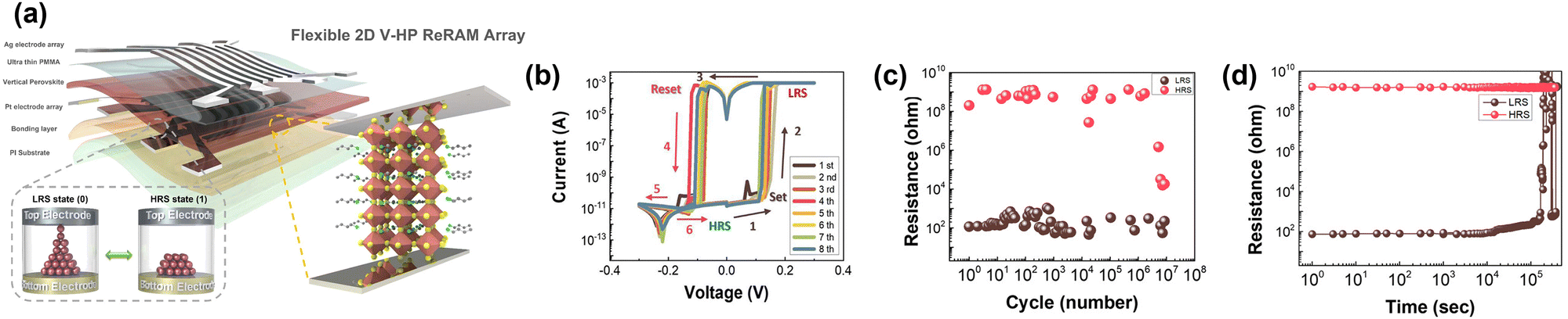 | ||
| Fig. 3 (a) The structure of a flexible memory device. (b) Eight times I–V curves of the flexible memory device. (c) Endurance cycles of the flexible memory device. (d) Retention time of the flexible memory device. Reproduced with permission from ref. 77. Copyright 2024, American Chemical Society. | ||
Although the Ag top electrode is frequently employed, the Cu electrode is also utilized in ECM-based halide perovskite memory devices.43,78,79 Jeon et al. introduced a pre-forming technique involving filament's random growth.80 These filaments are fully developed over the active layers during the pre-forming stage for device functionality, eliminating the necessity for additional forming processes, as shown in Fig. 4a. Following the etching process, the encapsulation layer and top electrodes were applied using the same technique. This process enables the memory device to acquire numerous randomly grown filaments. Using sacrificial layers during pre-forming enhances the filament length in the resistive switching film, reducing the forming voltage to the SET voltage level. Fig. 4b illustrates the I–V characteristics of both the reference and pre-formed Cu/SiNx/Pt devices. Fig. 4c and d present the TEM images of an ECM sample before and after the pre-forming process. The images illustrate the change in the morphology of the resistive switching layer resulting from filament generation. The indirect forming process is expected to reduce damage to the resistive switching film throughout the forming procedure. The endurance and retention properties of 8 cells were measured in both line and conventional samples, as illustrated in Fig. 4e and f, respectively.
 | ||
| Fig. 4 (a) Process flow of the pre-forming method. (b) I–V curves of reference and pre-formed devices. (c) TEM images of the devices before the pre-forming process. (d) TEM images of the devices after the pre-forming process. (e) Endurance cycles of reference and pre-formed devices. (f) Retention time of reference and pre-formed devices. Reproduced with permission from ref. 80. Copyright 2020, Elsevier. | ||
For the endurance test, we applied a +1.8 V/100 ns pulse during the SET process and a −1.8 V/100 ns pulse during the RESET process. The LRS and HRS currents were consistently recorded at 0.1 V throughout 107 switching cycles. The results indicate an enhancement in the endurance characteristics of the pre-formed samples. The retention was measured to illustrate the device's dependability under elevated temperature conditions. Notably, the degradation-free data retention property was observed for the ECM samples treated by the proposed methods, in contrast to the conventional sample. Both samples demonstrate outstanding memory retention capabilities at 105 seconds. Therefore, the suggested approach shows no decline in performance and enhances endurance with characteristics comparable to those of the traditional method.
Nickel (Ni) is also used because ionization occurs readily at the active metal, allowing the generated metal ions to traverse the insulator and accumulate on a counter electrode due to the reduction effect.81 Park et al. examined the configuration of the Ni/SiOx/ITO device in Fig. 5a.82Fig. 5b shows the I–V curve. Owing to the current overshoot phenomenon, focusing on the RESET process rather than the SET process is crucial. The Joule heating induced by a negative voltage leads to the dissolution of filaments, which in turn enhances the ON/OFF window.34,58,83 The ON/OFF ratio between the HRS and the LRS has been verified through the consecutive sweeping test illustrated in Fig. 5c. The ON-state current was 4.1 × 10⁴ times larger than the OFF-state current and remained stable until the device failed. Following the 87-switching cycle, there was a slight decrease in the ON/OFF ratio attributed to a transition failure in the HRS, yet the switching remained uniform.84 The problems in the HRS were evident not just during the endurance test but also in the retention evaluation. Fig. 5d illustrates the data in an OFF state that could not sustain its condition when subjected to a periodic read voltage of approximately −0.2 V. The LRS maintained its data for over 104 s, whereas the current increased from the HRS to the LRS at around 7500 s.
 | ||
| Fig. 5 (a) TEM image and the structure of the Ni/SiOx/ITO memory device. (b) I–V characteristics of the Ni/SiOx/ITO memory device. (c) Endurance cycles of the Ni/SiOx/ITO memory device. (d) Retention time of the Ni/SiOx/ITO memory device. Reproduced with permission from ref. 82. Copyright 2022, ELSEVIER. (e) Schematic illustration of the Zr/Ta2O5−x/Pt/SiO2/Si memory device. (f) I–V curves of the Zr/Ta2O5−x/Pt/SiO2/Si memory device. (g) Retention time of the Zr/Ta2O5−x/Pt/SiO2/Si memory device. (h) Endurance cycles of the Zr/Ta2O5−x/Pt/SiO2/Si memory device. Reproduced with permission from ref. 87. Copyright 2022, the Royal Society of Chemistry. | ||
In evaluating potential top electrodes for resistive switching memory devices, zirconium (Zr) is a less advantageous material than traditional top electrodes of ECM.85,86 This is primarily due to its strong affinity for oxygen, forming a durable passivating oxide, as indicated by the Gibbs free formation energy for metal–cation combinations.87,88 Raeis-Hosseini et al. focused on thoroughly examining the influence of the Zr electrode and empirically exploring its potential application in a Ta2O5-based ECM device.87 A Pt/Zr/Ta2O5−x/Pt configuration was employed to illustrate the memory device in Fig. 5e. In Fig. 5f, the Ta2O5−x-based memory devices exhibited the characteristic bipolar resistive switching behavior associated with ECM types. A thermodynamic-driving force in voltage was applied to the Zr active electrode, with the Pt bottom electrode grounded. The devices were activated in light of electroforming initiated at +4 V, resulting in a change between the LRS and the HRS. The I–V curves of the Pt/Zr/Ta2O5−x/Pt-based devices were evaluated using a DC sweeping voltage applied to the Zr top electrode. During the initial voltage sweep, the Zr top electrode had oxidation, changing to Zr4+; the cations generated a conducting filament at the Pt bottom interface by reducing to Zr atoms. Following the formation of the conducting filament, the switching layer was modified to represent the LRS. The conducting filament was ruptured by applying the opposite voltage, resulting in the device returning to the HRS. The retention time was tested to evaluate the stability of the Zr/Ta2O5−x/Pt device. An ON/OFF ratio of 102 was achieved, corresponding to findings from earlier studies, and there was no significant degradation in the current LRS and HRS (Fig. 5g). The endurance characteristics of the Ta2O5−x-based memory device demonstrate reliability over 100 cycles at a reading bias of 0.3 V. The observed stability highlights the strong memory characteristics of the devices featuring Zr electrodes (Fig. 5h).
Through the modification between the electrode and the resistive switching layer using an interlayer, a transition from valence change memories (VCMs) to ECM can occur. VCM is observed in metal oxides, particularly when anions are moved within the insulating layer.20,39,40,89 The redox reaction leads to a change in the valence state within the cation sublattice.50,70,90,91 Then, a change in the electronic conductivity within the insulating layer occurs. Lübben et al. modified the Ta electrode-Ta2O5 resistive switching layer interface using a graphene interlayer.92 The impact of a graphene monolayer film serving as an intermediary layer between Ta and Ta2O5 is associated with suppressing TaOx formation and oxygen evolution reactions.
The Ta/TaOx interface is essential in VCM switching processes, with the switching mechanism related to the passivation of the reduced TaOx phase or metallic Ta. This effect is more significant than the commonly accepted Schottky barrier theory. By modifying the Ta/TaOx interface through the introduction of monolayer graphene, the formation of TaOx is inhibited due to the chemical reaction between Ta5+ and O2− while also aiming to enhance the oxygen overpotential, which represents the energy barrier for the oxygen redox reaction.93
The electrochemical redox reactions occurring at the tantalum electrode concerning the oxygen processes exhibit considerable inhibition, resulting in the transition of the cell behavior from VCM to ECM operating modes. Therefore, graphene's capacity hinders oxygen redox reactions and ion diffusion at low voltages. Graphene dissolves virtually no oxygen and exhibits a significant overpotential for the electrode reaction. The monolayer graphene effectively prevents the diffusion of oxygen ions and atoms, ensuring they do not reach the Ta metal. This action inhibits the oxidation of oxygen ions under positive bias, thereby preventing the evolution of oxygen. The formation of Ta-ions and their involvement in the resistive switching process primarily account for the observed ECM characteristics. Additionally, the graphene layer exhibits electronic conductivity only in the in-plane direction while creating an energy barrier for electrons moving in the off-plane direction, resulting in a voltage drop. Consequently, it is anticipated that redox reactions will be suppressed.
3. TEM observation of the ECM mechanisms in resistive switching memory devices
TEM offers unique advantages over other characterization techniques, providing insight into the underlying ECM mechanisms in resistive switching devices. TEM enables visualization at the atomic scale, allowing direct observation of the nanoscale conductive filaments and interface dynamics that govern the resistive switching process, which is critical for identifying the specific structural and morphological changes that occur during filament formation and dissolution, ultimately influencing device performance and stability. Moreover, TEM can be readily integrated with analytical tools such as energy-dispersive X-ray spectroscopy (EDS) and electron energy loss spectroscopy (EELS). This combination allows simultaneous acquisition of structural and chemical information, making it possible to pinpoint the spatial distribution of metal ions and other constituent elements with sub-nanometer precision. As a result, the exact compositional changes in the conductive pathway can be correlated with observed structural modifications, providing a comprehensive understanding of the ECM mechanism at the atomic level. In situ TEM observation primarily provides a dynamic operation process of the resistive memories on the atomic scale. By applying external electrical bias directly inside the microscope using an in situ I–V holder, the evolution of conductive filaments, ion migration, and interface dynamics can be monitored in real time. This allows researchers to capture transient phenomena and map the time-dependent changes that occur as the device switches between different resistance states.This section will introduce previous studies that used TEM to elucidate ECM mechanisms in resistive-switching memory. TEM observations facilitate a deeper understanding of resistive switching phenomena, guiding the design and optimization of halide perovskite-based memory devices with improved performance and reliability. Because the experimental setup for in situ TEM is well-explained in the previous review report by Zhang et al.,94 the primary focus of this section is introducing a brief history, current issues, and utilizing state-of-the-art microscopic techniques for observing ECM mechanisms.
3.1. Microscopic observation of the ECM mechanism
This section introduces the previous works that directly observed the conductive filament by ex and in situ TEM. In 2007, Sakamoto et al. observed the precipitation of Cu in a solid electrolyte film using ex situ TEM, which provided conducting paths between Ta2O5 and Pt.95 After introducing an in situ TEM holder, in situ observing the dynamic process of filament formation is possible by applying voltages across the TEM samples. Xu et al. provided real-time, atomic-resolution insights into the switching behavior of a nanoscale Ag2S-based ionic conductor using in situ HRTEM. They demonstrated the reversible formation and dissolution of a conductive channel composed of argentite Ag2S and pure Ag nanocrystals under an applied bias, elucidating the phase transitions and atomic-scale mechanisms underlying resistance switching.96 Fujii et al. utilized in situ TEM to study the resistive switching behavior of Cu–GeS-based solid electrolyte devices. This approach provided real-time insights into the formation and dissolution of conducting filaments during resistance transitions between the HRS and the LRS. By directly observing the material under electrical bias, they provided real-time insights into the dynamic formation and dissolution of conducting filaments. Fig. 6a–e shows that under positive voltage, Cu ions migrated through the GeS matrix and reduced at the cathode to form nanocrystalline filaments, which acted as the conductive path for the LRS. These filaments were visually confirmed as deposits growing between the electrodes during voltage application. As the voltage polarity reversed (Fig. 6f–i), the conducting filaments shrank and eventually dissolved, leading to a transition back to the HRS. This behavior was directly linked to the device's switching characteristics, where the filament size correlated with current and resistance states. Selected area electron diffraction during the filament formation revealed sharp diffraction spots corresponding to Cu nanocrystals, while EDS analysis confirmed the composition of the filaments as predominantly Cu with minor Ge and S contributions. This voltage-dependent observation marked one of the first direct visualizations of conducting filament dynamics during resistive switching. It provided critical experimental evidence supporting the conductive-filament model. The study demonstrated the essential role of in situ TEM in elucidating nanoscale switching mechanisms, offering valuable insights into the design of reliable and scalable devices based on solid electrolytes.97 Yang et al. provided critical insights into filament dynamics in dielectric-based resistive memories. Through a combination of ex situ and in situ TEM studies, they revealed two distinct growth modes, including unexpected initiation of filaments from the active electrode, as well as dendritic structures that emphasized the role of cation transport, highlighting the dielectric/inert electrode interface as a crucial region for device optimization and challenged conventional ECM theories.98 Lv et al. conducted a systematic in situ TEM analysis of HfO2-based ECM cells to investigate endurance and retention failures during repetitive switching cycles, providing a clear correlation between cycling-induced filament changes and the degradation of switching performance, offering a basis for optimizing device reliability.25 Yoo et al. utilized high-resolution TEM to analyze bipolar resistive switching in amorphous Ge2Sb2Te5 (GST) films. Their study revealed the formation of crystalline tellurium filaments connecting inert electrodes, with the switching mechanism driven by Te-ion migration under an electric field.99 Hu et al. investigated the switching mechanisms in lightly oxidized ZnS-based ECM cells through high-resolution TEM analysis, discovering that a two-layer structure of ZnS films—comprising oxidized and unoxidized regions—confines filament formation and rupture to nanometer-thin interfaces, enabling highly stable, low-voltage operation. This research provided a pathway toward ultralow-power and ultrasensitive synaptic devices.100 Lee et al. conducted in situ TEM studies on Ta2O5-based memristors, demonstrating a significant suppression of ECM mechanisms through oxygen plasma-assisted electrode deposition. By reducing interface roughness and controlling oxygen–ion migration, the study revealed a dominant redox-driven valence change mechanism at the Ta2O5/TaO2 interface, enabling highly reliable multivalued conductance states over 1012 cycles. This work underscores the critical role of interface engineering in minimizing ECM-related variability and enhancing device performance.101 Simanjuntak et al. utilized TEM and EELS to investigate the effects of a neutral oxygen beam treatment on ZnO-based ECM devices. Their analysis revealed a significant reduction in oxygen vacancy concentrations near the surface of the ZnO film, as confirmed through depth-resolved EELS spectra.102 | ||
| Fig. 6 Series of TEM images captured during voltage application. The “+” and “−” symbols indicate the voltage polarity. Each image corresponds to points a to j marked in Fig. 1. (a) A Cu–GeS sample (A) contacted by a Pt–Ir tip (B). (b) and (c) A deposit appeared and expanded in the Cu–GeS under positive voltage, leading to a gradual decrease in resistance. (d) and (e) The deposit bridged the two Pt–Ir tips, causing a rapid resistance drop and saturation of the deposit size. (f) and (g) No changes were observed in the deposit, and the resistance remained low (LRS) during voltage sweeping. (h) The deposit suddenly shrank with an increase in negative voltage, resulting in a disconnection and a sharp rise in resistance. (i) The deposit completely disappeared. Reproduced with permission from ref. 90. Copyright 2011, AIP publishing. | ||
In recent years, studies utilizing TEM to investigate the ECM mechanism in resistive switching memory devices have focused on revealing the nanoscale dynamics of ion migration and conductive filament formation. These studies often aim to establish a deeper understanding of the structural and compositional changes occurring in various materials under electrical stimuli. However, research on ECM mechanisms in 2D material systems remains relatively scarce, with most efforts concentrating on traditional bulk or polycrystalline systems. This highlights the growing need to explore and extend TEM-based analysis to 2D systems to uncover their unique electrochemical behaviors and potential advantages for next-generation memory devices. Lee et al. demonstrated that single-crystalline CrPS4 can serve as a 2D layered solid electrolyte in electrochemical metallization (ECM) devices, where sulfur vacancies facilitate the migration of Ag ions to form and rupture conductive filaments, offering the potential for reliable and energy-efficient resistive switching devices.103 In the same year, 2020, Yoon et al. investigated a low-current ECM-like memristor using Ru as the mobile species in a Pt/Ta2O5/Ru structure, with in situ and ex situ TEM experiments providing critical insights into its resistive switching (RS) mechanism. High-resolution cross-sectional TEM images revealed the well-defined structure of the device, including a 5-nm-thick amorphous Ta2O5 layer, while EDS mapping confirmed the migration of Ru ions from the bottom electrode into the Ta2O5 layer during the SET process, forming discontinuous Ru-rich conducting filaments that established the LRS. During the RESET process, these filaments dissolved as Ru ions returned to the bottom electrode, restoring the HRS. Real-time in situ TEM observations further visualized this migration process, demonstrating the reversible and bias-dependent nature of Ru ion dynamics. Additional ion milling to the TEM sample was carried out for grounding under voltage bias, as shown in Fig. 7a. Fig. 7b shows the contact of the Au tip to the TEM sample. Conduction mechanism analysis revealed that tunneling conduction dominated in the LRS due to Ru nanoclusters, while hopping conduction was observed in the HRS and intermediate states (see Fig. 7c–e). The device's unique RS characteristics, including low switching current (<1 μA), long retention (∼100 years), and multilevel analog switching, were attributed to the high conductivity of RuOx suboxides and the dispersed nature of Ru ions. These findings underscore the advantages of Ru-based systems, with the TEM-based analysis providing a detailed understanding of their scalability down to sub-10 nm dimensions and their potential for advanced memory and neuromorphic applications.104 Similarly, Guo et al. demonstrated that the introduction of a SiO2/Ta2O5 heterojunction in ECM memristors confines the formation and dissolution of Ag conductive filaments within an ultra-thin Ta2O5 layer. Using TEM and EDS, they visualized inverted cone-shaped filaments and linked this morphology to the device's low switching voltage, high uniformity, and enhanced endurance.105 Li et al. uniquely utilized 2D covalent organic frameworks (COFs) as the matrix for resistive switching devices, a rare approach compared to previous studies focused on inorganic materials like oxides or chalcogenides. Through high-resolution TEM and EDS analyses, they revealed the confinement of Ag conductive filaments within COF channels, demonstrating enhanced control over filament dynamics, electroforming-free switching, and chemical adaptability, setting COF-based systems apart from conventional inorganic ECM devices.106 Yuan et al. investigated resistive switching and exchange bias control in a Si/SiO2/Ta/Pt/Ag/Mn-doped ZnO (MZO)/Pt/FeMn/Co/ITO device. Using aberration-corrected STEM and EDS, they directly visualized the formation and dissolution of Ag conductive filaments, which played a crucial role in the device's resistive switching. During the SET process under positive voltage, Ag ions migrated from the Ag anode and were reduced to Ag atoms within the MZO layer, forming conductive filaments that bridged the electrodes. These filaments were observed to penetrate the MZO and partially extend into the FeMn layer, inducing a transition to the LRS. Under reverse bias during the RESET process, the filaments dissolved near the MZO/Pt interface, restoring the HRS. The study highlighted the interplay between resistive switching and exchange bias modulation.107 Xue et al. introduced a novel approach to enhance resistive random-access memory performance by incorporating a Ni nanocone array into a conventional memristor structure, which was fabricated via a one-step electrodeposition process and integrated. TEM observation revealed cone-shaped conducting filaments confined to the nanocone regions, driven by the enhanced local electric field at the tip.108 Device consisting of one-dimensional (1D) nanotubes (NTs) instead of a thin film showed different ECM behavior. Liu et al. demonstrated that single Ta2O5 NT-based devices exhibit unique resistive switching characteristics, which contrast with thin-film devices, where ion migration and filament growth typically occur throughout the bulk of the dielectric layer, resulting in higher variability and forming voltages. The confined growth of Ag conductive filaments along the NT surface enabled lower forming voltages, higher filament stability, and selective surface switching, attributed to the unique 1D structure and enhanced ion mobility on the NT surface.109 The case of conductive-bridging random-access memory (CBRAM) devices, however, shows the different ECM mechanisms. Choi et al. reported the in situ observation of the Co/SiOx/TiN CBRAM device. Under an applied bias, Co filaments grew as nanoscale pillars from the Co electrode, extending into the SiOx layer. This electromigration-mediated filament process demonstrated clear morphological changes linked to resistive switching operation, highlighting Co's distinct behavior compared to conventional Ag or Cu-based CBRAM systems.110 Recent in situ TEM studies enabled demonstrating breakthroughs. A study by Casu et al. exemplifies the power of in situ TEM by capturing real-time filament evolution in gold cluster films, leading to a deeper understanding of ECM-like switching mechanisms. This level of dynamic insight would be impossible using ex situ techniques alone.111 It should be noted that the in situ TEM observations presented in this study were conducted on simplified planar structures. While these allow for precise control and imaging, they may not fully represent the behavior of stacked device architectures where interfacial effects, vertical diffusion, and confinement can alter key electrochemical kinetics. Efforts to bridge this gap have been reported using more realistic device-inspired platforms,112–114 which remain important directions for future work.
 | ||
| Fig. 7 (a) Bright-field TEM image of the fabricated individual nanopillar-type in situ TEM sample, and (b) depiction of the contact formation between the Au tip and the top electrode during bias application. (c)–(e) Cross-sectional in situ TEM images of the Pd/Pt (top)/Ta2O5/Ru (bottom) structured device, illustrating its pristine HRS, LRS, and RESET HRS. Reproduced with permission from ref. 98. Copyright 2020, Wiley. | ||
3.2. Applying 4D STEM
Recently, four-dimensional scanning transmission electron microscopy (4D STEM) has been increasingly adopted in various fields of materials research, allowing for a richer understanding of local structural, chemical, and electrostatic properties at the nanoscale. In a typical 4D STEM experiment, a focused electron probe is raster-scanned across the sample while a 2D diffraction pattern is recorded at every scan position, resulting in a comprehensive 4D dataset. This approach captures real-space information and provides reciprocal-space data that can be analyzed to reveal phase, strain, orientation, and electric field distributions within a material—capabilities that go well beyond conventional imaging or diffraction techniques.115–117 A study by Winkler et al. used in situ 4D STEM to explore the crystallization and microstructural evolution of HfO2 dielectric layers in RRAM devices. By observing the transformation of amorphous hafnia to its monoclinic crystalline phase during annealing, the study identified that the minimum crystallization temperature is 180 °C, significantly lower than previously reported values for thin films. This was attributed to texture transfer mechanisms from adjacent layers and the influence of pre-existing crystalline seeds. High-resolution TEM images, combined with fast Fourier transform (FFT) and azimuthal integration, revealed the progression of grain growth and the establishment of grain boundaries. Furthermore, automated crystal orientation mapping from 4D-STEM provided detailed insights into grain orientations and phase distributions, highlighting the critical role of adjacent TiN layers in directing crystallization and promoting texture alignment.118Beyond its demonstrated utility in mapping strain fields and identifying crystalline phases in complex materials, 4D STEM has shown promise for visualizing local electric and magnetic fields, primarily through differential phase contrast (DPC) analysis. By detecting subtle shifts in the center-of-mass of the diffraction pattern, DPC imaging enables quantitative mapping of the internal electric field at high spatial resolution. These capabilities have led to transformative insights across various systems, including ferroelectric domains, magnetic skyrmions, and nanoelectronic devices, where understanding nanoscale fields is paramount. Against this broad backdrop of applications, 4D STEM holds particular value for probing the electrochemical metallization (ECM) mechanism in resistive switching memory devices. In ECM-based devices, conductive filaments form and dissolve within an insulating matrix under applied voltage, governed by the migration of metal ions (e.g., Ag or Cu). By integrating 4D STEM with in situ biasing TEM holders, one can directly monitor how these filaments nucleate, grow, and disintegrate in real time, and simultaneously measure the spatial distribution of the electric field as it evolves. This unique combination of structural and field mapping data provides a holistic view of the ECM process, helping researchers correlate device-level switching characteristics with the underlying nanoscale dynamics. Ultimately, such insights from 4D STEM are expected to guide the design and optimization of next-generation resistive switching devices, bolstering their performance and reliability in emerging memory technologies.
4. Conclusions
The conductive filament mechanism was shown by analyzing the films’ resistance-changing properties in resistive switching systems. Ion migration from dielectric layers or electrodes is the primary resistive switching process. Despite substantial research using various materials to explain the observed resistance shifts, the mechanisms of resistance switching in memory devices are still debated. Although the conductive filament mechanism is known, the microscopic mechanisms, content, and morphology of its production and degradation are still debated. Oxygen vacancies, active metal cations, and anions dominate the filament. Resistive switching relies on dielectric material ion movement. ECM relies on cations moving from an electrode with electrochemical activity; hence, it deviates slightly. Ion migration and redox reactions in resistive switching occur at the nanoscale. Therefore, TEM is critical for understanding their dynamics. Unlike static ex situ TEM studies of device resistance states, in situ TEM permits real-time monitoring of resistive switching dynamics in situ. Unlike static ex situ TEM studies of device resistance states, in situ TEM permits real-time monitoring of resistive switching dynamics in situ. Metal atoms like Cu and Ag produce filaments in various material systems. The complicated kinetic parameters of ion migration and redox reactions determine the shape and direction of filament growth or dissolution, resulting in distinct filament growth patterns.This review explains the operation of the resistive switching memory device and the ECM. In addition, typical ex situ TEM investigations of various device resistance states show that in situ TEM allows real-time observations of resistive switching dynamics. In addition to characterizing existing systems, recent advances highlight the importance of exploring emerging electrode materials such as transition metal nitrides and two-dimensional layered conductors, which offer improved electrochemical stability and better compatibility with integration processes. Addressing fabrication challenges, including interface control and large-scale process uniformity, will be crucial for improving device reliability. These considerations may accelerate the real-world deployment of ECM-based nonvolatile memory technologies.
The TEM observation of conducting filament formation enables the investigation of the real-time nanostructure evolution process of resistive switching memory systems at atomic resolutions. This contributes to a deeper understanding of resistive switching behavior, potentially guiding improvements in the performance and reliability of memory devices. This review has the potential to be broadened to include additional electrodes featuring resistive switching material systems for ECM, thereby facilitating the rapid development of universal nonvolatile memory systems.
Author contributions
Woonbae Sohn: conceptualization, literature review, and writing – original draft. Hyerim Kim, Jung Hun Lee and Young-Seok Shim: literature review, and writing – review & editing. Cheon Woo Moon and Hyojung Kim: conceptualization, funding acquisition, supervision, and project administration.Data availability
No primary research results, software or code have been included and no new data were generated or analysed as part of this review.Conflicts of interest
There are no conflicts to declare.Acknowledgements
This work was supported by the National Research Foundation of Korea (NRF) grant funded by the Korea government (MSIT) (RS-2025-00554803), the National Research Foundation of Korea (NRF) grant funded by the Korean government (MSIT) (RS-2025-00555609), the Korea Basic Science Institute (National Research Facilities and Equipment Center) grant funded by the Ministry of Science and ICT (No. RS-2024-00402822), and the Faculty Research Fund of Sejong University in 2023.Notes and references
- H. Kim, B. Kang and C. Moon, Refractive Index Modulation for Metal Electrodeposition-Based Active Smart Window Applications, Micromachines, 2024, 15, 334 CrossRef PubMed.
- P. Kumar and D. Kaur, Multifunctionality in ferromagnetic shape memory alloy-based resistive switching memory for flexible ReRAM application, Appl. Phys. Lett., 2022, 121, 043503 CrossRef CAS.
- Z. Song, M. Hilal, H. S. Abdo, Z. Cai, H. Kim and J. I. Han, Synergistic ZnO-NiO composites for superior Fiber-Shaped Non-Enzymatic glucose sensing, J. Ind. Eng. Chem., 2025, 144, 691–699 CrossRef CAS.
- Y. Lin, X. Chen, Q. Zhang, J. You, R. Xu, Z. Wang and L. Sun, Nano device fabrication for in-memory and in-sensor reservoir computing, Int. J. Extreme Manuf., 2025, 7, 012002 CrossRef.
- H. Yuan, M. Hilal, Y. Ali, H. S. Abdo, Z. Cai, H. Kim, U. Ullah, H. Fayaz, W. Xie and J. I. Han, High-performance ZnO:CuO composite-based fiber-shaped electrode for non-enzymatic glucose sensing in biological fluids, Surf. Interfaces, 2024, 54, 105266 CrossRef CAS.
- J. Lee, H. Kim, M. Hilal and Z. Cai, Enhanced acetone gas sensor via TiO2 nanofiber-NiO nanoparticle heterojunction, Solid State Sci., 2024, 156, 107683 CrossRef CAS.
- S. Alam, M. Asaduzzaman Chowdhury, A. Shahid, R. Alam and A. Rahim, Synthesis of emerging two-dimensional (2D) materials – Advances, challenges and prospects, FlatChem, 2021, 30, 100305 CrossRef CAS.
- J. Lee, H. Kim, M. Hilal and Z. Cai, Core–shell SnO2/NiO p–n heterojunction composite for enhanced triethylamine gas sensitivity and selectivity, J. Mater. Sci.: Mater. Electron., 2024, 35, 1421 CrossRef CAS.
- H. Yoo, I. S. Lee, S. Jung, S. M. Rho, B. H. Kang and H. J. Kim, A Review of Phototransistors Using Metal Oxide Semiconductors: Research Progress and Future Directions, Adv. Mater., 2021, 33, 2006091 CrossRef CAS PubMed.
- H. Kim, G. Veerappan and J. H. Park, Conducting Polymer Coated Non-woven Graphite Fiber Film for Dye-Sensitized Solar Cells: Superior Pt- and FTO-Free Counter Electrodes, Electrochim. Acta, 2014, 137, 164–168 CrossRef CAS.
- J. Lee, H. Kim, M. Hilal and Z. Cai, Efficient acetone sensing utilizing Co3O4-Embedded porous ZnO nanofibers, J. Electroceram., 2024, 52, 283–296 CrossRef CAS.
- H. Kim, G. Veerappan, D. H. Wang and J. H. Park, Large Area Platinum and Fluorine-doped Tin Oxide-free Dye sensitized Solar Cells with Silver-Nanoplate Embedded Poly(3,4-Ethylenedioxythiophene) Counter Electrode, Electrochim. Acta, 2016, 187, 218–223 CrossRef CAS.
- G. Li, J. Hou, M. Hilal, H. Kim, Z. Chen, Y. Cui, J.-H. Kim and Z. Cai, Development of High-Performance Ethanol Gas Sensors Based on La2O3 Nanoparticles-Embedded Porous SnO2 Nanofibers, Sensors, 2024, 24, 6839 CrossRef CAS PubMed.
- R. Dittmann and J. P. Strachan, Redox-based memristive devices for new computing paradigm, APL Mater., 2019, 7, 110903 CrossRef.
- K. Fleck, N. Aslam, S. Hoffmann-Eifert, V. Longo, F. Roozeboom, W. M. M. Kessels, U. Böttger, R. Waser and S. Menzel, The influence of non-stoichiometry on the switching kinetics of strontium-titanate ReRAM devices, J. Appl. Phys., 2016, 120, 244502 CrossRef.
- K. Karmakar, A. Roy, S. Dhibar, S. Majumder, S. Bhattacharjee, B. Mondal, S. K. M. Rahaman, R. Saha, S. J. Ray and B. Saha, Instantaneous Gelation of a Self-Healable Wide-Bandgap Semiconducting Supramolecular Mg(II)-Metallohydrogel: An Efficient Nonvolatile Memory Design with Supreme Endurance, ACS Appl. Electron. Mater., 2023, 5, 3340–3349 CrossRef CAS.
- A. Roy, S. Dhibar, K. Karmakar, S. Some, S. A. Hafiz, S. Bhattacharjee, B. Saha and S. J. Ray, A Zn(II)-metal ion directed self-healing wide bandgap semiconducting supramolecular metallohydrogel: effective non-volatile memory design for in-memory computing, Mater. Adv., 2024, 5, 3459–3471 RSC.
- A. Roy, S. Dhibar, K. Karmakar, S. Bhattacharjee, B. Saha and S. J. Ray, Development of a novel self-healing Zn(II)-metallohydrogel with wide bandgap semiconducting properties for non-volatile memory device application, Sci. Rep., 2024, 14, 13109 CrossRef CAS PubMed.
- K. Karmakar, A. Roy, S. Dhibar, S. Majumder, S. Bhattacharjee, S. K. M. Rahaman, R. Saha, P. Chatterjee, S. J. Ray and B. Saha, Exploration of a wide bandgap semiconducting supramolecular Mg(II)-metallohydrogel derived from an aliphatic amine: a robust resistive switching framework for brain-inspired computing, Sci. Rep., 2023, 13, 22318 CrossRef CAS PubMed.
- H. Kim, K. A. Huynh, S. Y. Kim, Q. Van Le and H. W. Jang, 2D and Quasi-2D Halide Perovskites: Applications and Progress, Phys. Status Solidi RRL, 2020, 14, 1900435 CrossRef CAS.
- W. Kim, S. Menzel, D. J. Wouters, Y. Guo, J. Robertson, B. Roesgen, R. Waser and V. Rana, Impact of oxygen exchange reaction at the ohmic interface in Ta 2 O 5 -based ReRAM devices, Nanoscale, 2016, 8, 17774–17781 RSC.
- S. Rafiq, J. Hazra, M. Liehr, K. Beckmann, M. Abedin, J. S. Pannu, S. K. Jha and N. C. Cady, Investigation of ReRAM Variability on Flow-Based Edge Detection Computing Using HfO 2 -Based ReRAM Arrays, IEEE Trans. Circuits Syst., 2021, 68, 2900–2910 Search PubMed.
- K. S. Jaimes, H. P. Quiroz, J. A. Calderón and A. Dussan, Magnetic-resistive random access memories based on diluted Co-TiO2 nanotubes, Results Phys., 2024, 63, 107890 CrossRef.
- H. J. Kim, S. S. Kim, S. J. Park, Y. Oh and S. Han, Optimization of the fabrication process for TiOx/Al2O3 bilayer memristor to enhance the switching uniformity and reliability, J. Korean Ceram. Soc., 2025, 62, 504–514, DOI:10.1007/s43207-025-00491-4.
- H. Lv, X. Xu, H. Liu, R. Liu, Q. Liu, W. Banerjee, H. Sun, S. Long, L. Li and M. Liu, Evolution of conductive filament and its impact on reliability issues in oxide-electrolyte based resistive random access memory, Sci. Rep., 2015, 5, 7764 CrossRef CAS PubMed.
- J. Y. Park, Y. H. Lee, H. Kim and L. Dou, Two-dimensional perovskite heterostructures for single crystal semiconductor devices, J. Appl. Phys., 2023, 134, 060901 CrossRef CAS.
- M. Lübben, S. Menzel, S. G. Park, M. Yang, R. Waser and I. Valov, SET kinetics of electrochemical metallization cells: influence of counter-electrodes in SiO 2/Ag based systems, Nanotechnology, 2017, 28, 135205 CrossRef PubMed.
- H. Kim, D. Hyun, M. Hilal, Z. Cai and C. W. Moon, 2D and Quasi-2D Halide Perovskite-Based Resistive Switching Memory Systems, Electronics, 2024, 13, 3572 CrossRef.
- B. Cho, S. Song, Y. Ji, T. Kim and T. Lee, Organic Resistive Memory Devices: Performance Enhancement, Integration, and Advanced Architectures, Adv. Funct. Mater., 2011, 21, 2806–2829 CrossRef CAS.
- H. Kim, M. Choi, J. M. Suh, Y.-S. Shim, I. H. Im, D. Hyun, S. J. Yang, Z. Cai, M. Hilal, M. G. Lee, C. W. Moon, S. Y. Kim and H. W. Jang, Resistive random-access memories using quasi-2D halide perovskites for wafer-scale reliable switching behaviors, Mater. Sci. Semicond. Process., 2024, 182, 108718 CrossRef CAS.
- A. R. Patil, T. D. Dongale, R. K. Kamat and K. Y. Rajpure, Binary metal oxide-based resistive switching memory devices: A status review, Mater. Today Commun., 2023, 34, 105356 CrossRef CAS.
- H. Kim, J. S. Kim, J. Choi, Y.-H. Kim, J. M. Suh, M.-J. Choi, Y.-S. Shim, S. Y. Kim, T.-W. Lee and H. W. Jang, MAPbBr3 Halide Perovskite-Based Resistive Random-Access Memories Using Electron Transport Layers for Long Endurance Cycles and Retention Time, ACS Appl. Mater. Interfaces, 2024, 16, 2457–2466 CrossRef CAS PubMed.
- G. Ding, H. Li, J. Y. Zhao, K. Zhou, Y. Zhai, Z. Lv, M. Zhang, Y. Yan, S. T. Han and Y. Zhou, Nanomaterials for Flexible Neuromorphics, Chem. Rev., 2024, 124, 12738–12843 CrossRef CAS PubMed.
- J. S. Han, Q. Van Le, J. Choi, K. Hong, C. W. Moon, T. L. Kim, H. Kim, S. Y. Kim and H. W. Jang, Air-Stable Cesium Lead Iodide Perovskite for Ultra-Low Operating Voltage Resistive Switching, Adv. Funct. Mater., 2018, 28, 1705783 CrossRef.
- C. S. Hwang, Prospective of Semiconductor Memory Devices: from Memory System to Materials, Adv. Electron. Mater., 2015, 1, 1400056, DOI:10.1002/aelm.201400056.
- H. Kim, J. S. Han, J. Choi, S. Y. Kim and H. W. Jang, Halide Perovskites for Applications beyond Photovoltaics, Small Methods, 2018, 2, 1700310 CrossRef.
- M. K. Hota, J. A. Caraveo-Frescas, M. A. McLachlan and H. N. Alshareef, Electroforming-free resistive switching memory effect in transparent p -type tin monoxide, Appl. Phys. Lett., 2014, 104, 152104 CrossRef.
- S. Lee, K. H. Yun and D. Kim, Electroforming-less and multi-level resistive switching characteristics in tungsten oxide thin film, Thin Solid Films, 2019, 674, 91–96 CrossRef CAS.
- S. G. Kim, J. S. Han, H. Kim, S. Y. Kim and H. W. Jang, Recent Advances in Memristive Materials for Artificial Synapses, Adv. Mater. Technol., 2018, 3, 1800457 CrossRef.
- H. Kim, J. S. Han, S. G. Kim, S. Y. Kim and H. W. Jang, Halide perovskites for resistive random-access memories, J. Mater. Chem. C, 2019, 7, 5226–5234 RSC.
- A. Schönhals, C. M. M. Rosário, S. Hoffmann-Eifert, R. Waser, S. Menzel and D. J. Wouters, Role of the Electrode Material on the RESET Limitation in Oxide ReRAM Devices, Adv. Electron. Mater., 2018, 4, 1700243 CrossRef.
- S. G. Kim, Q. Van Le, J. S. Han, H. Kim, M. Choi, S. A. Lee, T. L. Kim, S. B. Kim, S. Y. Kim and H. W. Jang, Dual-Phase All-Inorganic Cesium Halide Perovskites for Conducting-Bridge Memory-Based Artificial Synapses, Adv. Funct. Mater., 2019, 29, 1906686 CrossRef CAS.
- E. Ambrosi, A. Bricalli, M. Laudato and D. Ielmini, Impact of oxide and electrode materials on the switching characteristics of oxide ReRAM devices, Faraday Discuss., 2019, 213, 87–98 RSC.
- S. Dueñas, H. Castán, O. G. Ossorio and H. García, Dynamics of set and reset processes on resistive switching memories, Microelectron. Eng., 2019, 216, 111032 CrossRef.
- G. Ghosh and M. K. Orlowski, Correlation between set and reset voltages in resistive RAM cells, Curr. Appl. Phys., 2015, 15, 1124–1129 CrossRef.
- L.-H. Wang, W. Yang, Q.-Q. Sun, P. Zhou, H.-L. Lu, S.-J. Ding and D. Wei Zhang, The mechanism of the asymmetric SET and RESET speed of graphene oxide based flexible resistive switching memories, Appl. Phys. Lett., 2012, 100, 063509 CrossRef.
- A. Ali, H. Abbas, M. Hussain, S. H. A. Jaffery, S. Hussain, C. Choi and J. Jung, Versatile GeS-based CBRAM with compliance-current-controlled threshold and bipolar resistive switching for electronic synapses, Appl. Mater. Today, 2022, 29, 101554 CrossRef.
- T. S. Lee, N. J. Lee, H. Abbas, H. H. Lee, T. S. Yoon and C. J. Kang, Compliance Current-Controlled Conducting Filament Formation in Tantalum Oxide-Based RRAM Devices with Different Top Electrodes, ACS Appl. Electron. Mater., 2020, 2, 1154–1161 CrossRef CAS.
- S. Slesazeck and T. Mikolajick, Nanoscale resistive switching memory devices: a review, Nanotechnology, 2019, 30, 352003 CrossRef CAS PubMed.
- J. Choi, J. S. Han, K. Hong, S. Y. Kim and H. W. Jang, Organic–Inorganic Hybrid Halide Perovskites for Memories, Transistors, and Artificial Synapses, Adv. Mater., 2018, 30, 1704002 CrossRef PubMed.
- Y. Huang, L. Tang, C. Wang, H. Fan, Z. Zhao, H. Wu, M. Xu, R. Shen, Y. Yang and J. Bian, Triple-Cation Perovskite Resistive Switching Memory with Enhanced Endurance and Retention, ACS Appl. Electron. Mater., 2020, 2, 3695–3703 CrossRef CAS.
- S. Lee, H. Kim, D. H. Kim, W. Bin Kim, J. M. Lee, J. Choi, H. Shin, G. S. Han, H. W. Jang and H. S. Jung, Tailored 2D/3D Halide Perovskite Heterointerface for Substantially Enhanced Endurance in Conducting Bridge Resistive Switching Memory, ACS Appl. Mater. Interfaces, 2020, 12, 17039–17045 CrossRef CAS PubMed.
- U. Chand, C.-Y. Huang, J.-H. Jieng, W.-Y. Jang, C.-H. Lin and T.-Y. Tseng, Suppression of endurance degradation by utilizing oxygen plasma treatment in HfO2 resistive switching memory, Appl. Phys. Lett., 2015, 106, 153502 CrossRef.
- S. Munjal and N. Khare, Advances in resistive switching based memory devices, J. Phys. D: Appl. Phys., 2019, 52, 433002 CrossRef CAS.
- J. S. Han, Q. Van Le, H. Kim, Y. J. Lee, D. E. Lee, I. H. Im, M. K. Lee, S. J. Kim, J. Kim, K. J. Kwak, M. Choi, S. A. Lee, K. Hong, S. Y. Kim and H. W. Jang, Lead-Free Dual-Phase Halide Perovskites for Preconditioned Conducting-Bridge Memory, Small, 2020, 16, 2003225 CrossRef CAS PubMed.
- D. Kumar, R. Aluguri, U. Chand and T. Y. Tseng, Metal oxide resistive switching memory: Materials, properties and switching mechanisms, Ceram. Int., 2017, 43, S547–S556 CrossRef CAS.
- C. Ye, J. Wu, G. He, J. Zhang, T. Deng, P. He and H. Wang, Physical Mechanism and Performance Factors of Metal Oxide Based Resistive Switching Memory: A Review, J. Mater. Sci. Technol., 2016, 32, 1–11 CrossRef CAS.
- H. Kim, M.-J. Choi, J. M. Suh, J. S. Han, S. G. Kim, Q. Van Le, S. Y. Kim and H. W. Jang, Quasi-2D halide perovskites for resistive switching devices with ON/OFF ratios above 109, NPG Asia Mater., 2020, 12, 21 CrossRef CAS.
- A. Prakash, D. Jana and S. Maikap, TaOx-based resistive switching memories: Prospective and challenges, Springer, 2013, vol. 8, p. 418 Search PubMed.
- R. Prakash and D. Kaur, Bipolar resistive switching behavior in Cu/AlN/Pt structure for ReRAM application, Vacuum, 2017, 143, 102–105 CrossRef CAS.
- A. Moazzeni, S. Hamedi and Z. Kordrostami, Switching characteristic of fabricated nonvolatile bipolar resistive switching memory (ReRAM) using PEDOT: PSS/GO, Solid State Electron., 2022, 188, 108208 CrossRef CAS.
- A. Lodhi, S. Saini, A. Dwivedi, A. Khandelwal and S. P. Tiwari, Bipolar resistive switching properties of TiOx/graphene oxide doped PVP based bilayer ReRAM, J. Micromech. Microeng., 2022, 32, 044001 CrossRef CAS.
- M. Ismail, E. Ahmed, A. M. Rana, I. Talib and M. Y. Nadeem, Coexistence of bipolar and unipolar resistive switching in Al-doped ceria thin films for non-volatile memory applications, J. Alloys Compd., 2015, 646, 662–668 CrossRef CAS.
- J. Kim, K. Jung, Y. Kim, Y. Jo, S. Cho, H. Woo, S. Lee, A. I. Inamdar, J. Hong, J.-K. Lee, H. Kim and H. Im, Switching Power Universality in Unipolar Resistive Switching Memories, Sci. Rep., 2016, 6, 23930 CrossRef CAS PubMed.
- S. Kossar, Impact of substrate temperature on NiO thin films for resistive switching memory (ReRAM) memory devices, Eng. Res. Express, 2024, 6, 015304 CrossRef CAS.
- Y. T. Chan, W. F. Chen, J. C. Wang and C. S. Lai, Effects of bottom electrode on resistive switching of silver programmable metallization cells with GdxOy/AlxOy solid electrolytes, Vacuum, 2017, 140, 30–34 CrossRef CAS.
- C. C. Hsu, Y. T. Chen and C. C. Tsao, Resistive random access memories fabricated by using solution-processed AlZnSnO semiconductor films and indium ball electrodes, J. Alloys Compd., 2017, 696, 697–700 CrossRef CAS.
- V. K. Perla, S. K. Ghosh and K. Mallick, Bipolar resistive switching behavior of carbon nitride supported copper oxide nanoparticles, Chem. Phys. Lett., 2020, 754, 137650 CrossRef CAS.
- K. Kaushlendra and D. Kaur, Multifunctional Resistive Switching in a Magnetization-Graded Ni/NiMnIn/V2O5 Flexible Heterostructure toward Brain-Inspired Neuromorphic Computing, ACS Appl. Electron. Mater., 2024, 6, 4548–4559 CrossRef CAS.
- J. S. Han, Q. Van Le, J. Choi, H. Kim, S. G. Kim, K. Hong, C. W. Moon, T. L. Kim, S. Y. Kim and H. W. Jang, Lead-Free All-Inorganic Cesium Tin Iodide Perovskite for Filamentary and Interface-Type Resistive Switching toward Environment-Friendly and Temperature-Tolerant Nonvolatile Memories, ACS Appl. Mater. Interfaces, 2019, 11, 8155–8163 CrossRef CAS PubMed.
- E. L. Lee, Y. S. Goh, A. S. M. A. Haseeb, Y. H. Wong, M. F. M. Sabri and B. Y. Low, Review—Electrochemical Migration in Electronic Materials: Factors Affecting the Mechanism and Recent Strategies for Inhibition, J. Electrochem. Soc., 2023, 170, 021505 CrossRef CAS.
- D. Woo, S. Jin, J. Kim, G. Park, W. Lee, M. Han, J. Kim, T. Shim, J. Park and J. Park, Unveiling the Resistive Switching Mechanism and Low Current Dynamics of Ru-based Hybrid Synaptic Memristors, Adv. Funct. Mater., 2025, 35, 2416309 CrossRef CAS.
- A. Korneluk and T. Stefaniuk, Multilevel Optical Storage, Dynamic Light Modulation, and Polarization Control in Filamented Memristor System, Adv. Mater., 2025, 37, 2411186 CrossRef CAS PubMed.
- B. Liao, Z. Chen, Y. Qiu, G. Zhang and X. Guo, Effect of citrate ions on the electrochemical migration of tin in thin electrolyte layer containing chloride ions, Corros. Sci., 2016, 112, 393–401 CrossRef CAS.
- A. Roy and P.-R. Cha, Electric field induced charge migration and formation of conducting filament during resistive switching in electrochemical metallization (ECM) memory cells, J. Appl. Phys., 2020, 128, 205102 CrossRef CAS.
- C. Wang, H. Wu, B. Gao, T. Zhang, Y. Yang and H. Qian, Conduction mechanisms, dynamics and stability in ReRAMs, Microelectron. Eng., 2018, 187–188, 121–133 CAS.
- S. J. Kim, I. H. Im, J. H. Baek, S. H. Park, J. Y. Kim, J. J. Yang and H. W. Jang, Reliable and Robust Two-Dimensional Perovskite Memristors for Flexible-Resistive Random-Access Memory Array, ACS Nano, 2024, 18, 28131–28141 CrossRef CAS PubMed.
- R. Prakash, S. Sharma, A. Kumar and D. Kaur, Improved resistive switching performance in Cu-cation migrated MoS2 based ReRAM device incorporated with tungsten nitride bottom electrode, Curr. Appl. Phys., 2019, 19, 260–265 CrossRef.
- G. Ghosh, Y. Kang, S. W. King and M. Orlowski, Role of CMOS Back-End Metals as Active Electrodes for Resistive Switching in ReRAM Cells, ECS J. Solid State Sci. Technol., 2017, 6, N1–N9 CrossRef CAS.
- D. S. Jeon, J. H. Park, D. Y. Kang, T. D. Dongale and T. G. Kim, Forming-ready resistance random access memory using randomly pre-grown conducting filaments via pre-forming, Mater. Sci. Semicond. Process., 2020, 110, 104951, DOI:10.1016/j.mssp.2020.104951.
- X. A. Tran, H. Y. Yu, Y. C. Yeo, L. Wu, W. J. Liu, Z. R. Wang, Z. Fang, K. L. Pey, X. W. Sun, A. Y. Du, B. Y. Nguyen and M. F. Li, A high-yield HfOx-based unipolar resistive ram employing Ni electrode compatible with Si-diode selector for crossbar integration, IEEE Electron Device Lett., 2011, 32, 396–398 CAS.
- M. Park, J. Park and S. Kim, Compatible resistive switching mechanisms in Ni/SiOx/ITO and application to neuromorphic systems, J. Alloys Compd., 2022, 903, 163870 CrossRef CAS.
- B. Gao, J. F. Kang, Y. S. Chen, F. F. Zhang, B. Chen, P. Huang, L. F. Liu, X. Y. Liu, Y. Y. Wang, X. A. Tran, Z. R. Wang, H. Y. Yu and A. Chin, 2011 International Electron Devices Meeting, IEEE, 2011, pp. 17.4.1–17.4.4 Search PubMed.
- N. Raghavan, K. L. Pey, W. Liu, X. Wu, X. Li and M. Bosman, Evidence for compliance controlled oxygen vacancy and metal filament based resistive switching mechanisms in RRAM, Microelectron. Eng., 2011, 88, 1124–1128 CrossRef CAS.
- Q. Liu, S. Long, H. Lv, W. Wang, J. Niu, Z. Huo, J. Chen and M. Liu, Controllable Growth of Nanoscale Conductive Filaments in Solid-Electrolyte-Based ReRAM by Using a Metal Nanocrystal Covered Bottom Electrode, ACS Nano, 2010, 4, 6162–6168 CrossRef CAS PubMed.
- M. Firdos, F. Hussain, M. Imran, M. Ismail, A. M. Rana, M. Arshad Javid, A. Majid, R. M. Arif Khalil and H. Ullah, Ab initio study of ceria films for resistive switching memory applications, Mater. Res. Express, 2017, 4, 106301 CrossRef.
- N. Raeis-Hosseini, S. Chen, C. Papavassiliou and I. Valov, Impact of Zr top electrode on tantalum oxide-based electrochemical metallization resistive switching memory: towards synaptic functionalities, RSC Adv., 2022, 12, 14235–14245 RSC.
- M. Lübben and I. Valov, Active Electrode Redox Reactions and Device Behavior in ECM Type Resistive Switching Memories, Adv. Electron. Mater., 2019, 5, 1800933 CrossRef.
- F. Cüppers, S. Menzel, C. Bengel, A. Hardtdegen, M. von Witzleben, U. Böttger, R. Waser and S. Hoffmann-Eifert, Exploiting the switching dynamics of HfO2-based ReRAM devices for reliable analog memristive behavior, APL Mater., 2019, 7, 091105 CrossRef.
- I. Valov and T. Tsuruoka, Effects of moisture and redox reactions in VCM and ECM resistive switching memories, J. Phys. D: Appl. Phys., 2018, 51, 413001 CrossRef.
- A. Ascoli, S. Menzel, V. Rana, T. Kempen, I. Messaris, A. S. Demirkol, M. Schulten, A. Siemon and R. Tetzlaff, A Deep Study of Resistance Switching Phenomena in TaOx ReRAM Cells: System-Theoretic Dynamic Route Map Analysis and Experimental Verification, Adv. Electron. Mater., 2022, 8, 2200182, DOI:10.1002/aelm.202200182.
- M. Lübben, P. Karakolis, V. Ioannou-Sougleridis, P. Normand, P. Dimitrakis and I. Valov, Graphene-Modified Interface Controls Transition from VCM to ECM Switching Modes in Ta/TaO x Based Memristive Devices, Adv. Mater., 2015, 27, 6202–6207 CrossRef PubMed.
- M. J. Lee, C. B. Lee, D. Lee, S. R. Lee, M. Chang, J. H. Hur, Y. B. Kim, C. J. Kim, D. H. Seo, S. Seo, U. I. Chung, I. K. Yoo and K. Kim, A fast, high-endurance and scalable non-volatile memory device made from asymmetric Ta2O5−xx/TaO2-xbilayer structures, Nat. Mater., 2011, 10, 625–630 CrossRef CAS PubMed.
- Y. Zhang, C. Wang and X. Wu, Review of electrical stimulus methods of in situ transmission electron microscope to study resistive random access memory, Nanoscale, 2022, 14, 9542–9552 RSC.
- T. Sakamoto, K. Lister, N. Banno, T. Hasegawa, K. Terabe and M. Aono, Electronic transport in Ta2O5 resistive switch, Appl. Phys. Lett., 2007, 91, 092110 CrossRef.
- Z. Xu, Y. Bando, W. Wang, X. Bai and D. Golberg, Real-Time In Situ HRTEM-Resolved Resistance Switching of Ag2S Nanoscale Ionic Conductor, ACS Nano, 2010, 4, 2515–2522 CrossRef CAS PubMed.
- T. Fujii, M. Arita, Y. Takahashi and I. Fujiwara, In situ transmission electron microscopy analysis of conductive filament during solid electrolyte resistance switching, Appl. Phys. Lett., 2011, 98, 212104 CrossRef.
- Y. Yang, P. Gao, S. Gaba, T. Chang, X. Pan and W. Lu, Observation of conducting filament growth in nanoscale resistive memories, Nat. Commun., 2012, 3, 732 CrossRef PubMed.
- S. Yoo, T. Eom, T. Gwon and C. S. Hwang, Bipolar resistive switching behavior of an amorphous Ge2Sb2Te5 thin films with a Te layer, Nanoscale, 2015, 7, 6340–6347 RSC.
- L. Hu, S. Fu, Y. Chen, H. Cao, L. Liang, H. Zhang, J. Gao, J. Wang and F. Zhuge, Ultrasensitive Memristive Synapses Based on Lightly Oxidized Sulfide Films, Adv. Mater., 2017, 29, 1606927, DOI:10.1002/adma.201606927.
- M.-J. Lee, G.-S. Park, D. H. Seo, S. M. Kwon, H.-J. Lee, J.-S. Kim, M. Jung, C.-Y. You, H. Lee, H.-G. Kim, S.-B. Pang, S. Seo, H. Hwang and S. K. Park, Reliable Multivalued Conductance States in TaO x Memristors through Oxygen Plasma-Assisted Electrode Deposition with in Situ-Biased Conductance State Transmission Electron Microscopy Analysis, ACS Appl. Mater. Interfaces, 2018, 10, 29757–29765 CrossRef CAS PubMed.
- F. M. Simanjuntak, T. Ohno and S. Samukawa, Neutral Oxygen Beam Treated ZnO-Based Resistive Switching Memory Device, ACS Appl. Electron. Mater., 2019, 1, 18–24 CrossRef CAS.
- M. J. Lee, S.-H. Kim, S. Lee, C. Yoon, K.-A. Min, H. Choi, S. Hong, S. Lee, J.-G. Park, J.-P. Ahn and B. H. Park, Understanding filamentary growth and rupture by Ag ion migration through single-crystalline 2D layered CrPS4, NPG Asia Mater., 2020, 12, 82 CrossRef CAS.
- J. H. Yoon, J. Zhang, P. Lin, N. Upadhyay, P. Yan, Y. Liu, Q. Xia and J. J. Yang, A Low-Current and Analog Memristor with Ru as Mobile Species, Adv. Mater., 2020, 32, 1904599 CrossRef CAS PubMed.
- X. Guo, Q. Wang, X. Lv, H. Yang, K. Sun, D. Yang, H. Zhang, T. Hasegawa and D. He, SiO2/Ta2O5 heterojunction ECM memristors: physical nature of their low voltage operation with high stability and uniformity, Nanoscale, 2020, 12, 4320–4327 RSC.
- T. Li, H. Yu, Z. Xiong, Z. Gao, Y. Zhou and S.-T. Han, 2D oriented covalent organic frameworks for alcohol-sensory synapses, Mater. Horiz., 2021, 8, 2041–2049 RSC.
- Y. Yuan, J. Qu, L. Wei, R. Zheng, Y. Lu, R. Liu, T. Liu, J. Chen, L. Luo, G. Du, B. You, W. Zhang, C. Zhang, L. Zhu, Y. Hu, Q. Xu and J. Du, Electric Control of Exchange Bias at Room Temperature by Resistive Switching via Electrochemical Metallization, ACS Appl. Mater. Interfaces, 2022, 14, 26941–26948 CrossRef CAS PubMed.
- Q. Xue, Y. Peng, L. Cao, Y. Xia, J. Liang, C.-C. Chen, M. Li and T. Hang, Ultralow Set Voltage and Enhanced Switching Reliability for Resistive Random-Access Memory Enabled by an Electrodeposited Nanocone Array, ACS Appl. Mater. Interfaces, 2022, 14, 25710–25721 CrossRef CAS PubMed.
- C.-J. Liu, H.-Y. Lo, A.-Y. Hou, J.-Y. Chen, C.-H. Wang, C.-W. Huang and W.-W. Wu, Observing resistive switching behaviors in single Ta2O5 nanotube-based memristive devices, Mater. Today Nano, 2022, 18, 100212 CrossRef CAS.
- Y.-J. Choi, S. Bang, T.-H. Kim, K. Hong, S. Kim, S. Kim, B.-G. Park and W. Y. Choi, Electric-Field-Induced Metal Filament Formation in Cobalt-Based CBRAM Observed by TEM, ACS Appl. Electron. Mater., 2023, 5, 1834–1843 CrossRef CAS.
- A. Casu, A. Chiodoni, Y. P. Ivanov, G. Divitini, P. Milani and A. Falqui, In Situ TEM Investigation of Thermally Induced Modifications of Cluster-Assembled Gold Films Undergoing Resistive Switching: Implications for Nanostructured Neuromorphic Devices, ACS Appl. Nano Mater., 2024, 7, 7203–7212 CrossRef CAS.
- Z. Q. Wang, H. Y. Xu, L. Zhang, X. H. Li, J. G. Ma, X. T. Zhang and Y. C. Liu, Performance improvement of resistive switching memory achieved by enhancing local-electric-field near electromigrated Ag-nanoclusters, Nanoscale, 2013, 5, 4490 RSC.
- K. Shin, Y. Kim, F. V. Antolinez, J. S. Ha, S. Lee and J. H. Park, Controllable Formation of Nanofilaments in Resistive Memories via Tip-Enhanced Electric Fields, Adv. Electron. Mater., 2016, 2, 1600233 CrossRef.
- K. Bejtka, G. Milano, C. Ricciardi, C. F. Pirri and S. Porro, TEM Nanostructural Investigation of Ag-Conductive Filaments in Polycrystalline ZnO-Based Resistive Switching Devices, ACS Appl. Mater. Interfaces, 2020, 12, 29451–29460 CrossRef CAS PubMed.
- C. Ophus, Four-Dimensional Scanning Transmission Electron Microscopy (4D-STEM): From Scanning Nanodiffraction to Ptychography and Beyond, Microsc. Microanal., 2019, 25, 563–582 CrossRef CAS PubMed.
- K. C. Bustillo, S. E. Zeltmann, M. Chen, J. Donohue, J. Ciston, C. Ophus and A. M. Minor, 4D-STEM of Beam-Sensitive Materials, Acc. Chem. Res., 2021, 54, 2543–2551 CrossRef CAS PubMed.
- W. Sohn, M. Kim and H. W. Jang, Atomic-Scale Insights into the 2D Materials from Aberration-Corrected Scanning Transmission Electron Microscopy: Progress and Future, Small Sci., 2024, 4, 2300073, DOI:10.1002/smsc.202300073.
- R. Winkler, A. Zintler, O. Recalde-Benitez, T. Jiang, D. Nasiou, E. Adabifiroozjaei, P. Schreyer, T. Kim, E. Piros, N. Kaiser, T. Vogel, S. Petzold, L. Alff and L. Molina-Luna, Texture Transfer in Dielectric Layers via Nanocrystalline Networks: Insights from in Situ 4D-STEM, Nano Lett., 2024, 24, 2998–3004 CrossRef CAS PubMed.
| This journal is © The Royal Society of Chemistry 2025 |