Doping molecular organic semiconductors by diffusion from the vapor phase†
Kelly A.
Peterson
 a,
Ashlea
Patterson
 a,
Alejandro
Vega-Flick
b,
Bolin
Liao
b and
Michael L.
Chabinyc
 *a
*a
aMaterials Department, University of California, Santa Barbara, California 93106, USA. E-mail: mchabinyc@engineering.ucsb.edu
bDepartment of Mechanical Engineering, University of California, Santa Barbara, California 93106, USA
First published on 26th August 2020
Abstract
Thin films of amorphous small molecule semiconductors are widely used in organic light emitting displays and have promising applications in solar cells and thermoelectric devices. Adding dopants increases the conductivity of organic semiconductors, but high concentrations of dopants can disrupt their structural ordering, alter the shape of the electronic density of states in the material, and increase the effects of Coulomb interactions on charge transport. Electrical doping of the solution processable hole-transport material 2,2′,7,7′-tetrakis[N,N-di(4-methoxyphenyl)amino]-9,9′-spirobifluorene (spiro-OMeTAD) was studied with 2,3,5,6-tetrafluoro-7,7,8,8-tetracyanoquinodimethane (F4TCNQ) as a p-type dopant. Infiltration of F4TCNQ from the vapor phase into films of spiro-OMeTAD provided a route to highly doped films with up to 39 ± 2 mol% doping. Structural characterization confirmed that the films remain amorphous even at the highest doping levels with no apparent phase separation. We quantitatively determined the carrier concentration using UV-Vis spectroscopy to interpret the evolution of the electrical conductivity. Over the range of carrier concentrations (1019–1020 1 cm−3), the electrical conductivity increased no more than linearly with carrier concentration, while the thermopower had a small increase with carrier concentration. The trends in conductivity and thermopower were related to the unique electronic structure of spiro-OMeTAD, which is able to support two carriers per molecule. Temperature-dependent conductivity measurements were used to further analyze the transport mechanism.
Introduction
Small molecule organic semiconductors have become widely used in organic light emitting devices (OLEDs) for information displays.1 Small molecules can be thermally evaporated to form smooth, glassy layers in devices. Amorphous films of organic semiconductors can also be cast from solvent and are used frequently as electron and hole transport layers in devices such as thin film solar cells.2,3 Doping of such transport layers is particularly beneficial to modify their electrical conductivity and to control the energetic line-up of transport levels at interfaces. The role of dopants on the structural ordering of amorphous materials has not been extensively studied,4 particularly if there is aggregation induced by charge transfer interactions.The electrical conductivity of thin films of amorphous small molecules have been found to follow an Arrhenius-type thermally activated hopping conduction model.5 The conductivity, σ, is given by eqn (1) where σ0 is the conductivity at infinite temperature with all carriers activated, Ea is the hopping activation energy, kB is the Boltzmann constant, and T is the temperature.
 | (1) |
One example of a solution-processable small molecule semiconductor that forms amorphous films is 2,2′,7,7′-tetrakis[N,N-di(4-methoxyphenyl)amino]-9,9′-spirobifluorene (spiro-OMeTAD) (Fig. 1a). This material is commonly used as a hole transport layer in perovskite solar cells3,11 and dye sensitized solar cells.12,13 In solar cells, spiro-OMeTAD is typically doped with LiTFSI, tert-butylpyridine, and oxygen to a conductivity ∼10−5 S cm−1 at 12–30 mol% LiTFSI.14 As shown in Fig. 1a, the core of the spiro-OMeTAD molecule has two fluorene units connected by a spiro-bridged carbon atom. Because of this spiro bridge, the two fluorene units are perpendicular to each other, and the molecular structure frustrates crystallization in thin films. Spiro-OMeTAD can be crystallized, leading to a triclinic P![[1 with combining macron]](https://www.rsc.org/images/entities/char_0031_0304.gif) structure with only short-range π–π overlap between adjacent molecules.15,16 The spiro-bridge also leads to a unique electronic structure relative to other materials. Density functional theory (DFT) calculations using the long-range corrected hybrid functional ωB97X-D reveal that the HOMO and HOMO−1 orbitals of spiro-OMeTAD in the experimental geometry from a single crystal structure are nearly degenerate and localize onto opposite sides of the spiro bridge.15,16 Our ωB97X-D/6-31G(d) calculations on an isolated molecule in vacuum without symmetry constraints show similar localization of the HOMO and HOMO−1 on the asymmetric structure that is likely present in amorphous films (Fig. 1b). Such long-range corrected hybrid DFT functionals are helpful to more accurately model the electronic structure of mixed-valence spiro compounds than functionals such as B3LYP that overly delocalize and mix the molecular orbitals.17 The impact of this near degeneracy on charge transport has not been examined in detail.
structure with only short-range π–π overlap between adjacent molecules.15,16 The spiro-bridge also leads to a unique electronic structure relative to other materials. Density functional theory (DFT) calculations using the long-range corrected hybrid functional ωB97X-D reveal that the HOMO and HOMO−1 orbitals of spiro-OMeTAD in the experimental geometry from a single crystal structure are nearly degenerate and localize onto opposite sides of the spiro bridge.15,16 Our ωB97X-D/6-31G(d) calculations on an isolated molecule in vacuum without symmetry constraints show similar localization of the HOMO and HOMO−1 on the asymmetric structure that is likely present in amorphous films (Fig. 1b). Such long-range corrected hybrid DFT functionals are helpful to more accurately model the electronic structure of mixed-valence spiro compounds than functionals such as B3LYP that overly delocalize and mix the molecular orbitals.17 The impact of this near degeneracy on charge transport has not been examined in detail.
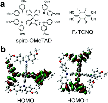 | ||
| Fig. 1 (a) Chemical structure of spiro-OMeTAD and F4TCNQ and (b) DFT calculations of spiro-OMeTAD's nearly degenerate HOMO and HOMO−1. Perpendicular fluorene units are both seen edge-on in (b). | ||
Here we examine spiro-OMeTAD as a model system to study charge transport in amorphous small molecule semiconductor films at high carrier concentrations. It has the advantage of being readily cast from solution into amorphous thin films and has a unique electronic structure relative to many molecular semiconductors. We doped spiro-OMeTAD films with small molecule dopant 2,3,5,6-tetrafluoro-7,7,8,8-tetracyanoquinodimethane (F4TCNQ) by infiltration from the vapor phase leading to a maximum of 39 ± 2 mol% F4TCNQ films. The electron affinity of F4TCNQ at 5.24 eV18 is close to Spiro-OMeTAD's first and second ionization energies, ≈5.1–5.3 eV.12 This close energy match between the dopant and host allowed us to study the effects of spiro-OMeTAD's two hopping sites on the material's electronic transport. We found that Seebeck coefficient and temperature-dependent conductivity measurements are consistent with a Gaussian density of charged states modified by the presence of spiro-OMeTAD2+ states.
Results & discussion
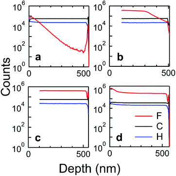
We doped spun-cast spiro-OMeTAD films by diffusing F4TCNQ vapor into the films, or “vapor doping” them with F4TCNQ. We and others have previously used this vapor-doping process to dope semiconducting polymers, including PBTTT and P3HT,19,20 but we are not aware of its use for molecular systems. Vapor doping differs from methods, such as thermal co-evaporation of host and dopant molecules or spin casting of doped solutions. Casting the neutral semiconductor prior to the doping process eliminates difficulties in the solubilization of the doped form of the semiconductor and its associated counterion that can preclude achieving high levels of doping. For the vapor doping process, the spiro-OMeTAD films were placed face-down in the top of a doping chamber in a N2 atmosphere glovebox. A small amount of F4TCNQ was placed in the bottom of the doping chamber. When the doping chamber is heated on a hot plate at 200 °C, the F4TCNQ sublimates and can diffuse into the film. The glass transition temperature, Tg, of spiro-OMeTAD is relatively high at 124 °C.21 In our apparatus, the substrate temperature is not fixed and after 15 min of heating, the substrate reaches 92.5 °C, and ∼106 °C after 90 min of heating, so Tg of spiro-OMeTAD is never exceeded during the doping process (see ESI† for full heating curve).We determined whether F4TCNQ had diffused through the full depth of the film during vapor doping using secondary ion mass spectroscopy (SIMS). Fluorine atoms provide a unique maker for the presence of F4TCNQ; we note that due to the high fluorine signal level, the amount of F4TCNQ could not be accurately quantified relative to other atoms using our SIMS instrument. In Fig. 2a, 15 min of vapor doping leads to a concentration profile where the concentration of F4TCNQ is greatest near the surface of the film and decreases to the instrument noise level at the bottom of the film. After 30 min of vapor doping, Fig. 2b, F4TCNQ has nearly diffused through the full depth of the film. F4TCNQ can fully diffuse through the film with a roughly even concentration profile after 45 min of vapor doping, as seen in Fig. 2c. To test whether the uneven concentration profiles caused by vapor doping could be leveled through annealing, we annealed a 30 min vapor doped film for 10 min at 140 °C. This annealing temperature was chosen because it is above spiro-OMeTAD's glass transition temperature of 124 °C but below the temperature at which F4TCNQ sublimes from films, 150 °C.22Fig. 2d shows that the concentration profile of the annealed film was more even at the bottom of the film than the unannealed film (Fig. 2b). Ten minutes was long enough for F4TCNQ to diffuse through the film without much de-doping but was not long enough for the film to crystallize. In the 45 and 75 min doped films, crystallization was observed around the edges of the film after annealing. Films used for charge transport measurements were annealed to reduce concentration gradients, and partially crystallized areas of annealed films were not measured.
We used grazing incidence wide angle X-ray scattering (GIWAXS) to determine if either spiro-OMeTAD or F4TCNQ crystallized (or co-crystallized) during the doping procedure. In the scattering from the undoped film, Fig. 3a, a broad, nearly isotropic ring of scattering was observed around q ≈ 1.25 Å−1. This indicates that the film has an amorphous structure, as expected for spiro-OMeTAD, which is known to generally form glassy films. In Fig. 2b, the scattering for an 80 min F4TCNQ vapor doped film showed a similar, nearly isotropic scattering pattern and no signatures of scattering at d-spacings known for crystalline form of F4TCNQ.23 Because this 80 min doping time is higher than the doping times used for charge transport measurements, the X-ray scattering patterns indicate that the doped films retain their amorphous structure throughout the vapor doping process, as opposed to forming a co-crystal or phase separating.
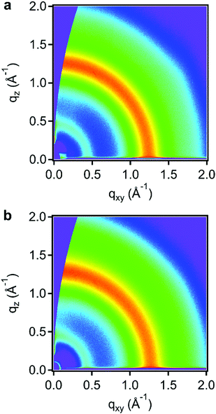 | ||
| Fig. 3 Grazing incidence wide angle X-ray scattering images of (a) neat and (b) 80 min F4TCNQ vapor doped spiro-OMeTAD. | ||
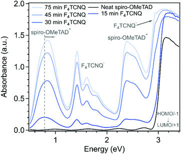
To understand the nature of the charge transfer process between spiro-OMeTAD and F4TCNQ, we measured the UV-Vis-NIR absorbance as a function of doping time (Fig. 4). The absorbance spectrum of undoped spiro-OMeTAD has an onset around 3 eV with weak sub-optical gap features in the spectrum due to interference effects from the ∼500 nm thick film. Upon doping, new features were observed in the spectra that confirm that integer charge transfer (ICT) occurred between F4TCNQ and spiro-OMeTAD. Two spectra regions have features that can be assigned to the F4TCNQ anion: the vibronic series between 1.3–2 eV and the peak at 2.9 eV.24 The features centered around 0.8 eV and 2.5 eV can be assigned to transitions of spiro-OMeTAD+ or spiro-OMeTAD2+. Spiro-OMeTAD+ and spiro-OMeTAD2+ have an additional weak transition centered at 1.77 eV.25 In our spectra, that peak is obscured by the stronger F4TCNQ anion absorbance. Due to the degenerate HOMO and HOMO−1 of spiro-OMeTAD, spiro-OMeTAD+ still has a transition at 3 eV. At high doping levels, the feature centered around 0.8 eV becomes less symmetric and shows a blueshift. This blueshift suggests that some population of spiro-OMeTAD molecules has been oxidized to the 2+ state by two F4TCNQ molecules. The energy gap between the HOMO−1 and HOMO levels was calculated to shift from 0.37 to 0.95 eV when spiro-OMeTAD+ is oxidized to the 2+ triplet state.26 Because spiro-OMeTAD is a mixed-valence compound with two degenerate oxidation states, spiro-OMeTAD2+ may be in a triplet state or an open-shell singlet state.
Because spiro-OMeTAD and F4TCNQ undergo integer charge transfer, we used UV-Vis-NIR spectra to estimate the charge carrier concentration in the doped films. In disordered organic semiconductors with hopping conduction, the carrier concentration cannot be measured readily using the Hall effect. Instead, we used the absorbance of F4TCNQ− to estimate the hole concentration. The area under the F4TCNQ− peaks between 1.25–2.15 eV is proportional to the concentration of F4TCNQ− anions in the films. We fit the three F4TCNQ− peaks and the spiro-OMeTAD+ transition at 1.77 eV to determine the area of the F4TCNQ− absorbance. We used reference spectra of [Cp*2Co][F4TCNQ] and [Cp*2Fe][F4TCNQ] solutions to calculate a reference value of the molar extinction coefficient, ε of the F4TCNQ− optical absorbance. With the F4TCNQ− absorbance, film thickness, and molar extinction coefficient, the concentration of F4TCNQ− in each film can be calculated (see ESI,† for full description of fitting methods). The number of F4TCNQ− is equivalent to the number of electrons removed from spiro-OMeTAD and spiro-OMeTAD+. The UV-Vis spectra cannot easily be used to distinguish the relative amounts of spiro-OMeTAD+ and spiro-OMeTAD2+, therefore it is difficult to measure how the holes are distributed on the two possible oxidation sites of a spiro-OMeTAD molecule. While some spiro-OMeTAD+ polarons could condense to spiro-OMeTAD2+ bipolarons, the shape of the NIR peak suggests that both could be present in the doped films.
On average, films doped to our maximum doping time of 75 min reached a carrier concentration of 3.3 ± 0.3 × 1020 cm−3, which is estimated to correspond to a film composition of 39 ± 2 mol% F4TCNQ based on the concentration of F4TCNQ− determined by UV-Vis and the density of spiro-OMeTAD films.27 (see ESI† for details) Because the vapor doping process adds mass to the spiro-OMeTAD films, the thickness or density of the films can change. We found that film thicknesses increased from ≈420 ± 20 nm for undoped films to ≈530 ± 30 nm for films doped for 45 and 75 min. With this increase in film thickness, the density of spiro-OMeTAD hopping sites would decrease. Based on a spiro-OMeTAD film density of 1.02 g cm−3,27 the molecule density of spiro-OMeTAD films is 5.02 × 1020 cm−3. Because the HOMO and HOMO−1 of spiro-OMeTAD are nearly degenerate, each molecule has two potential electronic states, giving a hopping site density of 1 × 1021 cm−3.
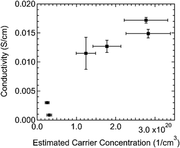
We measured the room temperature conductivity of several samples with different doping levels. We found that the conductivity generally increases with doping level, with a maximum of 0.017 S cm−1 (Fig. 5). This value is two orders of magnitude higher than the conductivity reached by typical LiTFSI doping14 and similar to the 0.024 S cm−1 reported for LiTFSI and benzoyl peroxide doping.28 Estimating with σ = qpμ, we found that the electrical mobility may decrease but remains on the order of 10−4 cm2 V−1 s−1. (see Fig. S8, ESI†) The mobility of these films cannot be measured directly because they are too disordered for Hall effect measurements, and field-effect transistor and space charge limited current (SCLC) mobility measurements are not accurate on highly doped films. For comparison, the Mott-Gurney SCLC mobility of undoped glassy spiro-OMeTAD was 2.3 × 10⁻⁴ cm2 V−1 s−1.29 Many doped small molecule systems show a superlinear increase in conductivity with doping, such as MeO-TPD:F6TCNNQ's increase over a dopant![[thin space (1/6-em)]](https://www.rsc.org/images/entities/char_2009.gif) :
:![[thin space (1/6-em)]](https://www.rsc.org/images/entities/char_2009.gif) host density ratio range of 0.01–0.29.9 In our measurements of spiro-OMeTAD:F4TCNQ, the increase in conductivity with hole concentration is no greater than linear, which could be attributed to this decrease in hole mobility.
host density ratio range of 0.01–0.29.9 In our measurements of spiro-OMeTAD:F4TCNQ, the increase in conductivity with hole concentration is no greater than linear, which could be attributed to this decrease in hole mobility.
To find the activation energy of hopping, Ea, in this system, we measured the conductivity of films with varying doping levels over a temperature range of at least 140–295 K (see Fig. S9, ESI†). The dependence of the electrical conductivity on temperature followed the Arrhenius relationship of eqn (1) with a nearly constant Ea ≈ 170 meV (Fig. 6). Ea decreases with increasing doping level and can level off at high doping levels.7 The constant (or slightly decreasing) trend of Ea in this carrier concentration range is consistent with Ea leveling off at high doping levels. A broad range of p-type materials has been reported to have Ea values 171–295 meV.7 Our measurements of Ea were on films with greater than 10 mol% doping, but spiro-OMeTAD:F4TCNQ is among the systems with lower Ea values. For comparison, 2,2′,7,7′-tetrakis(N,N-diphenylamino)-9.9-spirobifluorene (spiro-TAD):F6TCNNQ system has similar physical and electronic properties to spiro-OMeTAD:F4TCNQ and its Ea is 180 meV at 10 mol% doping.30 Both spiro-TAD:F6TCNNQ and spiro-OMeTAD:F4TCNQ have very small host IE-dopant EA offsets ∼0.1 eV. Interestingly the electrical conductivity of spiro-OMeTAD:F4TCNQ is significantly higher than that of spiro-TAD:F6TCNNQ despite the comparable value of Ea.
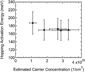 | ||
| Fig. 6 Hopping activation energy (Ea) was roughly constant with carrier concentration in this range. Error in Ea was estimated at 15%, while error in the carrier concentration was estimated at 20%. | ||
One model proposes that electrical conduction in highly doped small molecule organic semiconductors primarily takes place among host-dopant charge transfer complexes, which form a DOS with width σICTC.7 Based on data from a wide variety of p- and n-type host:dopant systems at 10 mol% doping, a relationship between σICTC determined by ultraviolet photoemission spectroscopy (UPS) and Ea, as well as the material's carrier density, was determined. Using the reported empirical relationship between Ea and σICTC, doped films of spiro-OMeTAD are expected to have a low σICTC. Spiro-OMeTAD has a low molecular density in doped films of 5 × 1020 cm−3, similar to other materials that are reported to have a low σICTC. The roughly constant Ea of spiro-OMeTAD:F4TCNQ over this doping range suggests that the disorder of integer charge transfer complexes is roughly constant over this doping range, as well.
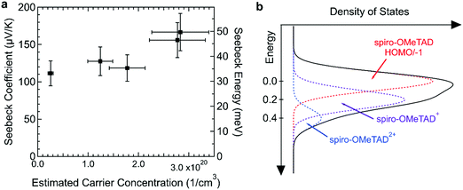
We measured the in-plane Seebeck coefficient, S, of the doped spiro-OMeTAD films with varying carrier concentrations at room temperature to assess how the shape of the electronic DOS changes with doping (Fig. 7a). Because spiro-OMeTAD has two potential sites for charge hopping, it is of interest to determine if there are signs that both oxidation states are involved in charge transport. The Seebeck coefficient is related to the shape of the DOS through the Mott formalism,31
 | (2) |
 | (3) |
We found that S was roughly constant in this carrier concentration range with a small increase at high carrier concentrations ≈2.8 × 1020 cm−3. The three points below 2 × 1020 cm−3 have an average value of 119 μV K−1, while the values at higher concentrations are 156 and 167 μV K−1. Typically, the Seebeck coefficient of small molecule semiconductors decreases with increasing dopant concentration.9 Because the Seebeck constant is related to the distance between Etr and EF by eqn (3), Etr–EF in spiro-OMeTAD:F4TCNQ may have increased at ≈2.8 × 1020 cm−3. The increase in Etr–EF could be caused by a change in DOS shape by spiro-OMeTAD2+ states. Upon doping, a Gaussian density of spiro-OMeTAD+ states forms that overlaps with the Gaussian DOS of spiro-OMeTAD. As the carrier concentration increases, it is possible that bipolarons could form, further extending the tail of the DOS and potentially increasing Etr–EF. This mechanism of increasing the Seebeck coefficient has been observed and modeled in polymer blends.32,33Fig. 7b shows a schematic of how the densities of charged states could look when the spiro-OMeTAD DOS using three Gaussian functions each with a width of 0.1 eV and with centers spaced 0.2 eV apart. The total number of states used was 1 × 1021 cm−3, with a carrier concentration of 3 × 1020 cm−3 and 25% of charged molecules in the bipolaron state. These parameters were an approximation based on typical parameters for amorphous small molecules and the properties of F4TCNQ:spiro-OMeTAD. Differential pulse voltammetry measurements in solvent have shown that the first three oxidation potentials of spiro-OMeTAD are −5.15, −5.27, and −5.48 eV.12 However, the exact spacing of neutral, 1+, and 2+ states may change in the solid state, especially if the dielectric constant of the film changes with doping. In addition to changing the shape of the DOS, bipolarons have also been associated with an increase in Seebeck coefficient in hopping semiconductors through an increase in vibrational entropy.34
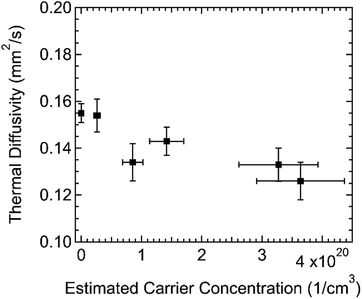
To complement these studies, we studied the changes in thermal transport in spiro-OMeTAD films with doping. We measured the in-plane thermal diffusivity of films with varying carrier concentrations with a transient grating technique.35 The transient gradient apparatus uses a visible wavelength laser (515 nm or 2.4 eV) to induce a periodic thermal expansion in the sample. Spiro-OMeTAD+ and spiro-OMeTAD2+ absorb at this wavelength, so the doped films could be measured without any change in sample preparation. Because undoped spiro-OMeTAD films are transparent to the pump laser, we prepared a dyed spiro-OMeTAD film by blade-coating a film from a solution of Oil Red O and spiro-OMeTAD in chlorobenzene. The thermal diffusivity of this pink-dyed film of insulating spiro-OMeTAD was 0.155 ± 0.004 mm2 s−1. The thermal diffusivity of F4TCNQ vapor-doped films, shown in Fig. 8, was roughly constant, or slightly decreasing, with carrier concentration in the range measured.
The thermal conductivity can be calculated from the product of the thermal diffusivity, density, and specific heat capacity. We measured the specific heat capacity of spiro-OMeTAD powder with modulated differential scanning calorimetry (0.9 J kg−1 °C−1) and took the density of spiro-OMeTAD films as 1.02 g cm−3.27 With these values, we find an in-plane thermal conductivity for spiro-OMeTAD of 0.14 W m−1 K−1. This thermal conductivity is similar to measurements on other amorphous molecules of 0.14–0.15 W m−1 K−1.36 For comparison, undoped C60 and its derivatives have even lower thermal conductivity of ≈0.06 W m−1 K−1,37 while undoped films of semiconducting polymers can have thermal conductivities of ≈0.2 to 2 W m−1 K−1 depending on the crystallinity and molecular orientation.38–41 The thermal conductivity of doped samples will depend on changes in density or heat capacity, but we can expect that the former is unlikely to increase more than ≈20% (based on the density of crystalline spiro-OMeTAD) and the latter by a comparable factor. Any expected change due to these factors would be relatively small and would tend to bring the thermal conductivity of the doped samples to the same level as the undoped samples. This result is not surprising given the low electrical conductivity of the doped samples but does show that the intermolecular interactions of the charged molecules likely do not substantially modify the thermal conductivity of the amorphous films. The resulting thermoelectric figure of merit is quite low, ZT = 0.8 × 10⁻⁴ at room temperature.
Conclusions
We used vapor infiltration to dope spiro-OMeTAD films with F4TCNQ up to 39 ± 2 mol% F4TCNQ. Although spiro-OMeTAD can crystallize in neutral form, the doped films remained amorphous. Our results show that this doping method can be used to reach a high conductivity relative to other doped p-type small molecules and provides a convenient route to study doping in small molecules. An increase in the Seebeck coefficient at ≈2.8 × 10²⁰ 1 cm−3 suggested that the presence of spiro-OMeTAD2+ in the films changes the shape of the DOS. Finally, we found that the thermal diffusivity of spiro-OMeTAD is similar to other amorphous organic materials and does not change significantly with doping. Our findings also suggest that degenerate frontier orbitals may change the thermoelectric properties of organic semiconductors and could be a useful molecular design parameter.Conflicts of interest
There are no conflicts of interest to declare.Acknowledgements
This work was supported by the National Science Foundation (NSF) under DMR 1808622. Portions of this work were carried out at the MRL Shared Experimental Facilities, supported by the NSF MRSEC program under award no. DMR 1720256. Use of the Stanford Synchrotron Radiation Lightsource, SLAC National Accelerator Laboratory, is supported by the U.S. Department of Energy, Office of Science, Office of Basic Energy Sciences under Contract No. DE-AC02-76SF00515. Use was made of computational facilities purchased with funds from the National Science Foundation (CNS-1725797) and administered by the Center for Scientific Computing (CSC). The CSC is supported by the California NanoSystems Institute (CNSI) and the MRSEC (NSF DMR 1720256) at UC Santa Barbara. We acknowledge the use of the Nanostructures Cleanroom Facility within the CNSI, supported by UC Santa Barbara and the UC Office of the President. A. P. was funded by the FLAM program under NSF award no. DMR 1460656. A. V. and B. L. acknowledges the support of a Sony Faculty Research Award for the thermal transport measurements. We thank Kathryn A. O’Hara and Naveen R. Venkatesan for assistance with GIWAXS measurements and Tom Mates for assistance with SIMS.References
- S. R. Forrest, Organic Electronics: Foundations to Applications, Oxford University Press, Oxford, 2020 Search PubMed.
- L. Calió, S. Kazim, M. Grätzel and S. Ahmad, Hole-Transport Materials for Perovskite Solar Cells, Angew. Chem., Int. Ed., 2016, 55, 14522–14545 CrossRef PubMed.
- J. Urieta-Mora, I. García-Benito, A. Molina-Ontoria and N. Martín, Hole transporting materials for perovskite solar cells: a chemical approach, Chem. Soc. Rev., 2018, 47, 8541–8571 RSC.
- A. P. Proudian, M. B. Jaskot, D. R. Diercks, B. P. Gorman and J. D. Zimmerman, Atom Probe Tomography of Molecular Organic Materials: Sub-Dalton Nanometer-Scale Quantification, Chem. Mater., 2019, 31, 2241–2247 CrossRef.
- K. Walzer, B. Maennig, M. Pfeiffer and K. Leo, Highly Efficient Organic Devices Based on Electrically Doped Transport Layers, Chem. Rev., 2007, 107, 1233–1271 CrossRef PubMed.
- V. I. Arkhipov, P. Heremans, E. V. Emelianova and H. Bässler, Effect of doping on the density-of-states distribution and carrier hopping in disordered organic semiconductors, Phys. Rev. B: Condens. Matter Mater. Phys., 2005, 71, 045214 CrossRef.
- M. Schwarze, C. Gaul, R. Scholz, F. Bussolotti, A. Hofacker, K. S. Schellhammer, B. Nell, B. D. Naab, Z. Bao, D. Spoltore, K. Vandewal, J. Widmer, S. Kera, N. Ueno, F. Ortmann and K. Leo, Molecular parameters responsible for thermally activated transport in doped organic semiconductors, Nat. Mater., 2019, 18, 242–248 CrossRef PubMed.
- R. Schmechel, Hopping transport in doped organic semiconductors: A theoretical approach and its application to p-doped zinc-phthalocyanine, J. Appl. Phys., 2003, 93, 4653–4660 CrossRef CAS.
- T. Menke, D. Ray, H. Kleemann, M. P. Hein, K. Leo and M. Riede, Highly efficient p-dopants in amorphous hosts, Org. Electron., 2014, 15, 365–371 CrossRef CAS.
- A. Fediai, F. Symalla, P. Friederich and W. Wenzel, Disorder compensation controls doping efficiency in organic semiconductors, Nat. Commun., 2019, 10, 4547 CrossRef PubMed.
- Z. Hawash, L. K. Ono and Y. Qi, Recent Advances in Spiro-MeOTAD Hole Transport Material and Its Applications in Organic–Inorganic Halide Perovskite Solar Cells, Adv. Mater. Interfaces, 2018, 5, 1700623 CrossRef.
- W. H. Nguyen, C. D. Bailie, E. L. Unger and M. D. McGehee, Enhancing the Hole-Conductivity of Spiro-OMeTAD without Oxygen or Lithium Salts by Using Spiro(TFSI)2 in Perovskite and Dye-Sensitized Solar Cells, J. Am. Chem. Soc., 2014, 136, 10996–11001 CrossRef CAS PubMed.
- T. Leijtens, J. Lim, J. Teuscher, T. Park and H. J. Snaith, Charge Density Dependent Mobility of Organic Hole-Transporters and Mesoporous TiO2 Determined by Transient Mobility Spectroscopy: Implications to Dye-Sensitized and Organic Solar Cells, Adv. Mater., 2013, 25, 3227–3233 CrossRef CAS.
- A. Abate, T. Leijtens, S. Pathak, J. Teuscher, R. Avolio, M. E. Errico, J. Kirkpatrik, J. M. Ball, P. Docampo, I. McPherson and H. J. Snaith, Lithium salts as “redox active” p-type dopants for organic semiconductors and their impact in solid-state dye -sensitized solar cells, Phys. Chem. Chem. Phys., 2013, 15, 2572–2579 RSC.
- D. Shi, X. Qin, Y. Li, Y. He, C. Zhong, J. Pan, H. Dong, W. Xu, T. Li, W. Hu, J.-L. Brédas and O. M. Bakr, Spiro-OMeTAD single crystals: Remarkably enhanced charge-carrier transport via mesoscale ordering, Sci. Adv., 2016, 2, e1501491 CrossRef PubMed.
- Y. Li, H. Li, C. Zhong, G. Sini and J.-L. Brédas, Characterization of intrinsic hole transport in single-crystal spiro-OMeTAD, npj Flexible Electron., 2017, 1, 2 CrossRef.
- T. Körzdörfer and J.-L. Brédas, Organic Electronic Materials: Recent Advances in the DFT Description of the Ground and Excited States Using Tuned Range-Separated Hybrid Functionals, Acc. Chem. Res., 2014, 47, 3284–3291 CrossRef PubMed.
- W. Gao and A. Kahn, Controlled p-doping of zinc phthalocyanine by coevaporation with tetrafluorotetracyanoquinodimethane: A direct and inverse photoemission study, Appl. Phys. Lett., 2001, 79, 4040–4042 CrossRef CAS.
- S. N. Patel, A. M. Glaudell, K. A. Peterson, E. M. Thomas, K. A. O’Hara, E. Lim and M. L. Chabinyc, Morphology controls the thermoelectric power factor of a doped semiconducting polymer, Sci. Adv., 2017, 3, e1700434 CrossRef.
- E. Lim, K. A. Peterson, G. M. Su and M. L. Chabinyc, Thermoelectric Properties of Poly(3-hexylthiophene) (P3HT) Doped with 2,3,5,6-Tetrafluoro-7,7,8,8-tetracyanoquinodimethane (F4TCNQ) by Vapor-Phase Infiltration, Chem. Mater., 2018, 30, 998–1010 CrossRef CAS.
- T. Malinauskas, D. Tomkute-Luksiene, R. Sens, M. Daskeviciene, R. Send, H. Wonneberger, V. Jankauskas, I. Bruder and V. Getautis, Enhancing Thermal Stability and Lifetime of Solid-State Dye-Sensitized Solar Cells via Molecular Engineering of the Hole-Transporting Material Spiro-OMeTAD, ACS Appl. Mater. Interfaces, 2015, 7, 11107–11116 CrossRef CAS PubMed.
- J. Li, C. W. Rochester, I. E. Jacobs, S. Friedrich, P. Stroeve, M. Riede and A. J. Moulé, Measurement of Small Molecular Dopant F4TCNQ and C60F36 Diffusion in Organic Bilayer Architectures, ACS Appl. Mater. Interfaces, 2015, 7, 28420–28428 CrossRef CAS.
- J. E. Cochran, M. J. N. Junk, A. M. Glaudell, P. L. Miller, J. S. Cowart, M. F. Toney, C. J. Hawker, B. F. Chmelka and M. L. Chabinyc, Molecular Interactions and Ordering in Electrically Doped Polymers: Blends of PBTTT and F4TCNQ, Macromolecules, 2014, 47, 6836–6846 CrossRef CAS.
- D. A. Dixon, J. C. Calabrese and J. S. Miller, Crystal and molecular structure of the 2:1 charge-transfer salt of decamethylferrocene and perfluoro-7,7,8,8-tetracyano-p-quinodimethane: [[Fe(C5Me5)2] +.cntdot.]2[TCNQF4]2−. The electronic structure of [TCNQF4]n (n = 0, 1-, 2-), J. Phys. Chem., 1989, 93, 2284–2291 CrossRef CAS.
- U. Bach, PhD thesis, École Polytechnique Fédérale de Lausanne, 2000.
- S. Fantacci, F. De Angelis, M. K. Nazeeruddin and M. Grätzel, Electronic and Optical Properties of the Spiro-MeOTAD Hole Conductor in Its Neutral and Oxidized Forms: A DFT/TDDFT Investigation, J. Phys. Chem. C, 2011, 115, 23126–23133 CrossRef CAS.
- P. Docampo, A. Hey, S. Guldin, R. Gunning, U. Steiner and H. J. Snaith, Pore Filling of Spiro-OMeTAD in Solid-State Dye-Sensitized Solar Cells Determined Via Optical Reflectometry, Adv. Funct. Mater., 2012, 22, 5010–5019 CrossRef CAS.
- Q. Liu, L. Fan, Q. Zhang, A. Zhou, B. Wang, H. Bai, Q. Tian, B. Fan and T. Zhang, Benzoyl Peroxide as an Efficient Dopant for Spiro-OMeTAD in Perovskite Solar Cells, ChemSusChem, 2017, 10, 3098–3104 CrossRef CAS PubMed.
- J. A. Röhr, X. Shi, S. A. Haque, T. Kirchartz and J. Nelson, Charge Transport in Spiro-OMeTAD Investigated through Space-Charge-Limited Current Measurements, Phys. Rev. Appl., 2018, 9, 044017 CrossRef.
- F. Zhang and A. Kahn, Investigation of the High Electron Affinity Molecular Dopant F6-TCNNQ for Hole-Transport Materials, Adv. Funct. Mater., 2017, 1703780 Search PubMed.
- N. F. Mott and E. A. Davis, Electronic processes in non-crystalline materials, Oxford University Press, Oxford, 2nd edn, 1979 Search PubMed.
- G. Zuo, X. Liu, M. Fahlman and M. Kemerink, High Seebeck Coefficient in Mixtures of Conjugated Polymers, Adv. Funct. Mater., 2017, 1703280 Search PubMed.
- A. Abtahi, S. Johnson, S. M. Park, X. Luo, Z. Liang, J. Mei and K. R. Graham, Designing π-conjugated polymer blends with improved thermoelectric power factors, J. Mater. Chem. A, 2019, 7, 19774–19785 RSC.
- D. Emin, Enhanced Seebeck coefficient from carrier-induced vibrational softening, Phys. Rev. B: Condens. Matter Mater. Phys., 1999, 59, 6205–6210 CrossRef CAS.
- A. Vega-Flick, D. Jung, S. Yue, J. E. Bowers and B. Liao, Reduced thermal conductivity of epitaxial GaAs on Si due to symmetry-breaking biaxial strain, Phys. Rev. Mater., 2019, 3, 034603 CrossRef CAS.
- X. Xie, K. Yang, D. Li, T.-H. Tsai, J. Shin, P. V. Braun and D. G. Cahill, High and low thermal conductivity of amorphous macromolecules, Phys. Rev. B, 2017, 95, 035406 CrossRef.
- X. Wang, C. D. Liman, N. D. Treat, M. L. Chabinyc and D. G. Cahill, Ultralow thermal conductivity of fullerene derivatives, Phys. Rev. B: Condens. Matter Mater. Phys., 2013, 88, 075310 CrossRef.
- J. C. Duda, P. E. Hopkins, Y. Shen and M. C. Gupta, Thermal transport in organic semiconducting polymers, Appl. Phys. Lett., 2013, 102, 251912 CrossRef.
- H. Ushirokita and H. Tada, In-plane Thermal Conductivity Measurement of Conjugated Polymer Films by Membrane-based AC Calorimetry, Chem. Lett., 2016, 45, 735–737 CrossRef CAS.
- J. Liu, X. Wang, D. Li, N. E. Coates, R. A. Segalman and D. G. Cahill, Thermal Conductivity and Elastic Constants of PEDOT:PSS with High Electrical Conductivity, Macromolecules, 2015, 48, 585–591 CrossRef CAS.
- A. Roy, T. L. Bougher, R. Geng, Y. Ke, J. Locklin and B. A. Cola, Thermal Conductance of Poly(3-methylthiophene) Brushes, ACS Appl. Mater. Interfaces, 2016, 8, 25578–25585 CrossRef CAS.
Footnote |
| † Electronic supplementary information (ESI) available. See DOI: 10.1039/d0qm00442a |
| This journal is © the Partner Organisations 2020 |

