Single crystal field-effect transistor of tetrabenzoporphyrin with a one-dimensionally extended columnar packing motif exhibiting efficient charge transport properties†
Juanjuan
Zhu
a,
Hironobu
Hayashi
 *a,
Meng
Chen
b,
Chengyi
Xiao
 b,
Kyohei
Matsuo
 a,
Naoki
Aratani
 a,
Lei
Zhang
*b and
Hiroko
Yamada
 *a
*a
aDivision of Materials Science, Nara Institute of Science and Technology (NAIST), 8916-5 Takayama-cho, Ikoma, Nara 630-0192, Japan. E-mail: hhayashi@ms.naist.jp; hyamada@ms.naist.jp
bBeijing Advanced Innovation Center for Soft Matter Science and Engineering & State Key Laboratory of Organic–Inorganic Composites, Beijing University of Chemical Technology, Beijing 100029, P. R. China. E-mail: zhl@buct.edu.cn
First published on 9th September 2021
Abstract
5,15-Bis(triisopropylsilyl)ethynyltetrabenzoporphyrin (TIPS-H2BP) gave a one-dimensionally extended columnar packing motif. The single crystal field-effect transistor of TIPS-H2BP exhibited clearly better hole mobility (2.16 cm2 V−1 s−1) than its metal complexes (ca. 0.1 cm2 V−1 s−1), with efficient charge transport through π–π stacking along the tetrabenzoporphyrin units.
The charge transport in organic semiconductors is achieved by the π orbital overlapping of the conjugated molecules along the direction of carrier flow. Therefore, organic semiconducting materials with a rigid and planar π-system have great potential to provide suitable packing to increase the π orbital overlap.1–4 Due to the large and rigid π-system, tetrabenzoporphyrins (BPs) are promising candidates as efficient p-type semiconducting materials.5,6 However, BP itself is hardly soluble in organic solvents, resulting in difficulty in its direct solution deposition. In addition, the solubility is an important factor not only for the solution-processable device fabrication but also for achieving the large-scale synthesis by conventional organic chemistry together with easy purification using column chromatography. Although these factors, including rigidity and solubility, are likely a trade-off relationship, several molecules perfectly satisfy these requirements. For example, 6,13-bis(triisopropylsilylethynyl)pentacene (TIPS-Pen), which is a benchmark compound as an efficient organic semiconducting material, has proven to be quite successful, despite the fact that the pentacene itself is almost insoluble in common organic solvents.7 Taking advantage of the improved solubility by the introduction of TIPSethynyl groups, the solution sharing with a micropillar-patterned blade gave a hole mobility up to 11 cm2 V−1 s−1,8 achieving clearly better hole mobility than pristine pentacene.
For BPs as well, recent synthetic efforts have solved the solubility problem by using the “precursor method”, in which a soluble precursor compound, 1,4:8,11:15,18:22,25-tetraethano-29H,31H-tetrabenzo[b,g,l,q]porphyrin (CP), can be quantitatively converted to BP by a thermally induced retro-Diels–Alder reaction with heating at 150–200 °C for several minutes.6,9 Importantly, the retro-Diels–Alder reaction releases only ethylene molecules as gaseous byproducts. Thus, no purification process is required to obtain pure compounds, if the corresponding precursors are sufficiently pure. The charge-carrier mobility of BP polycrystalline film obtained via the precursor method was evaluated for the first time by Aramaki, exhibiting a hole mobility of 0.017 cm2 V−1 s−1.10 The hole mobility was then slightly improved to 0.07 cm2 V−1 s−1, while the value was still low.11 Recently, the substituent effect was evaluated to obtain better charge transport property by controlling the packing orientation of BP. It was found that 5,15-bis(triisopropylsilylethynyl)-BP (TIPS-H2BP) with reasonable solubility for solution-processed organic thin film transistors formed two types of packing motifs: columnar motif using a drop-casting method and brickwork motif using a dip-coating method.12 The drop-casting films with the columnar motif showed low hole mobility (0.027 cm2 V−1 s−1), although such a columnar motif is also known to exhibit efficient charge transport properties. On the other hand, the brickwork motif has two dimensionally extended π-stacking. The maximum hole mobility of dip-coating films reached 1.1 cm2 V−1 s−1, which was approximately 14 times higher than pristine free-base BP (0.07 cm2 V−1 s−1). This disparity in charge transport property derived from different packing motifs prepared using drop-casting and dip-coating methods turned our attention to single-crystal field-effect transistors (SCFETs), which are able to unveil the intrinsic charge transport property of organic semiconducting materials due to ordered arrangement of molecules, free of grain boundaries and minimized defects. The obtained maximum hole mobility of TIPS-H2BP in the above report12 implied that functionalized BP derivatives could be candidates for efficient organic semiconducting materials. For further structural fine-tuning of BP, the potential of TIPS-H2BP as a simple prototype is necessary to be evaluated by using the single crystal.13–16 In this study, single crystals of TIPS-H2BP and its metal complexes were prepared on a substrate, and the molecular orientation in the single crystal was explored in detail. Then, the relationship between the molecular orientation and charge transport property was investigated by preparing SCFETs.
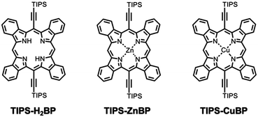
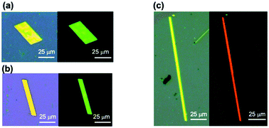
TIPS-H2BP and the zinc(II) and copper(II) complexes (TIPS-ZnBP and TIPS-CuBP) were synthesized by following the previous reports (Fig. 1).17 Then, their crystals were grown by drop-casting the toluene solution on the octadecyltrichlorosilane (OTS) modified Si/SiO2 surface. It was found that slow evaporation of the drop-casted toluene solution gave isolated and thin ribbon-shaped single crystals on Si/SiO2/OTS substrates (Fig. 2). Importantly, the changing of interfacial color in the polarized optical microscope (POM) images indicated that they were single crystals. Narrow ribbon-shaped crystals of TIPS-H2BP similar to the case of TIPS-CuBP were also observed. However, out-of-plane X-ray diffraction (XRD) and transmission electron microscopy (TEM) analyses indicated that the molecular orientations in these crystals were the same (vide infra). Indeed, the crystal grew having a different shape probably because of the slightly different surface energy on the substrate.18 Here, the order of ease of crystal formation was as follows: TIPS-H2BP > TIPS-ZnBP > TIPS-CuBP. Specifically, single crystals of TIPS-CuBP suitable for SCFETs were hardly obtained on a Si/SiO2/OTS substrate, usually giving a fiber-like structure (Fig. S1, ESI†).
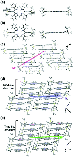
Before examining the molecular orientation of single crystals on a substrate, the bulk single crystal structures for each BP derivative were analyzed in order to establish a referential basis for further discussion. Those single crystals were prepared from toluene solutions, although the X-ray analysis had already been done with single crystals obtained from a different solvent system in the previous report.12,17 In fact, solvents showed no significant effect on their packing structures. Briefly, a large TIPS-H2BP core (Fig. 3a and b) formed a one-dimensionally extended columnar π-stacking motif with the plane-to-plane distance of BP of ca. 3.3 Å (Fig. 3c).18TIPS-H2BP molecules stacked orthogonally in the packing, alternately possessing a planar TIPS-H2BP molecule (Fig. 3a) and the one with two TIPSethynyl groups bent from the BP plane sigmoidally (Fig. 3b). It is evident that the well-ordered alignment of TIPS-H2BP facilitates the intermolecular charge transport in the column. BP backbones of TIPS-ZnBP19 and TIPS-CuBP20 are similar to TIPS-H2BP. However, molecules in the single crystal form a triad-like structure in which the molecules are stacked orthogonally.17 In the triad-like structure, TIPS-ZnBP and TIPS-CuBP also have the plane-to-plane distance of ca. 3.3 Å, while the triad units are packed parallel to provide one-dimensional slip-stacked structures. In addition, a planar TIPS-ZnBP or TIPS-CuBP molecule is sandwiched by the respective metal complexes with sigmoidally bent TIPSethynyl groups in the triad-like structure. As a result, long-range molecular orientation is missing in the cases of TIPS-ZnBP and TIPS-CuBP, in contrast with that observed in TIPS-H2BP.
To shed light on the molecular orientation of single crystals on a substrate, out-of-plane XRD analysis was performed (Fig. 4 and Fig. S2, ESI†). In the case of TIPS-H2BP (Fig. 4a), the intense peaks at 2θ = 5.16° with a d-spacing of 17.1 Å together with peaks at 2θ = 6.10° (d-spacing = 14.5 Å) and at 2θ = 6.22° (d-spacing = 14.2 Å) were well-consistent with the simulated [001], [010], and [011] diffractions of the one-dimensional columnar structure (Fig. 3c), respectively, according to the crystallographic data for the bulk crystal. These results support the fact that the one-dimensional columnar packing in parallel to the substrate was grown through the π–π stacking direction of TIPS-H2BP. Note that a peak at 4.66°, which corresponds to [001] of the brickwork motif,12 was not observed. Similarly, the peaks at 2θ = 5.02° (d-spacing = 17.6 Å) and at 2θ = 5.77° (d-spacing = 15.3 Å) for TIPS-ZnBP are in good agreement with the simulated [001] and [010] diffractions of the TIPS-ZnBP columnar structure, respectively (Fig. 4b). In the case of TIPS-CuBP, small peaks at 2θ = 5.03° (d-spacing = 17.6 Å) and at 2θ = 5.82° (d-spacing = 15.2 Å) which correspond to [001] and [010], respectively, could be observed (Fig. 4c), while less number of single-crystals on the substrate resulted in the overall weak peak intensity of the XRD pattern. As described above, a fiber-like structure also formed on the substrate together with ribbon-shaped crystals (Fig. S1, ESI†). Rigid π-systems could form the crystalline nanofibers.21,22 Thus, these crystalline fibers account for the peaks at 2θ = 4.87° and 2θ = 5.16° which are not consistent with the simulated patterns of the one-dimensional columnar packing.
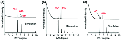 | ||
| Fig. 4 Experimental out-of-plane XRD and simulated powder XRD patterns of (a) TIPS-H2BP, (b) TIPS-ZnBP, and (c) TIPS-CuBP. | ||
In order to confirm the molecular arrangements in the ribbon-shaped crystals, TEM images and their corresponding selected area electron diffraction (SAED) patterns were collected from an individual ribbon-shaped crystal (Fig. 5). The observed bright diffraction spots demonstrated the high-quality of crystallinity. Here, the SAED pattern could be indexed with its single crystal structure, while the SAED patterns for TIPS-H2BP and TIPS-ZnBP are not complete. It was found that the preferred crystal growth directions of TIPS-H2BP, TIPS-ZnBP, and TIPS-CuBP were expected to be [100], [−111], and [−111], respectively (Fig. 3c–e), which are in good agreement with the morphologies predicted through the Bravais–Friedel–Donnay–Harker (BFDH)23–25 method (Fig. 5). Thus, SAED patterns and TEM analysis together with XRD measurement indicated that the growth direction of the ribbon-shaped crystals on the substrate was guided by π–π interactions, creating a one-dimensionally extended packing motif as a charge-carrier transport.
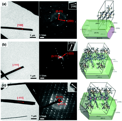 | ||
| Fig. 5 Representative TEM image, corresponding SAED pattern, and theoretically predicted growth morphology by using the BFDH method of (a) TIPS-H2BP, (b) TIPS-ZnBP, and (c) TIPS-CuBP single crystals. | ||
Finally, the charge transport property of the single crystals was evaluated by fabricating bottom-gate-top-contact organic field-effect transistors using the “gold layer glue technique”.26 Briefly, gold source and drain electrodes were placed on the crystals which were grown by drop-casting the toluene solution on the Si/SiO2/OTS substrate. The effective channel length and width were measured by microscopy (Fig. S3, ESI†).
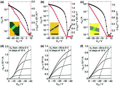
The ribbon-shaped crystals of TIPS-H2BP exhibited an average value of 1.16 cm2 V−1 s−1 with 15 devices (Fig. 6a and d), giving the maximum hole mobility of 2.16 cm2 V−1 s−1 with a threshold voltage Vth of 15.6 V and on/off ratio Ion/Ioff of 6.1 × 10² (Fig. S4, ESI†). In the previous report, the one-dimensional columnar structure of TIPS-H2BP prepared using the drop-casting method exhibited the hole mobility of 0.027 cm2 V−1 s−1.6 Thus, the maximum hole mobility obtained in this study is approximately 80 times higher than that obtained using the drop-casting method. This result supported the fact that the molecular orientation of TIPS-H2BP is preferable to SCFETs, with the charge transport through π–π stacking of BP units in the one-dimensional column. In addition, the efficient charge transport reflected the feature of single crystals free of grain boundaries and with minimized defects. It should be noted that nearly identical curves were observed after 10 cycles (Fig. S5, ESI†), suggesting the good bias-stress stability of SCFETs based on ribbon-shaped crystals of TIPS-H2BP. Here, SCFET devices based on TIPS-H2BP often showed the hole carried on operation mode especially for the device which exhibited a high hole mobility (Fig. S4, ESI†), indicating that the transport channel already formed even without gate bias (VG = 0 V). This is probably due to the high hole density of TIPS-H2BP. The holes not only filled the trap states, but also the excess holes became free carriers, forming a conducting channel even though at VG = 0 V. Moreover, the decreased trap states would facilitate carrier transport, thus improving the mobility of TIPS-H2BP.27
On the other hand, the ribbon-shaped crystals of the metal complexes, TIPS-ZnBP and TIPS-CuBP, showed clearly lower hole mobilities compared with TIPS-H2BP (Fig. 6b, c, e, f and Fig. S4, ESI†), although those values were much higher than the ones prepared using the spin-coating method (1.1 × 10⁻⁵ cm2 V−1 s−1 for TIPS-ZnBP and 5.6 × 10⁻³ cm2 V−1 s−1 for TIPS-CuBP).17 The maximum hole mobility of 0.12 cm2 V−1 s−1 (average values of 0.05 cm2 V−1 s−1 with 12 devices) with a threshold voltage Vth of 6.6 V and on/off ratio Ion/Ioff of 7.6 × 10⁵ for TIPS-ZnBP, while TIPS-CuBP showed the maximum hole mobility of 0.16 cm2 V−1 s−1 (average values of 0.14 cm2 V−1 s−1 with 4 devices) with a threshold voltage Vth of 3.0 V and on/off ratio Ion/Ioff of 1.1 × 10³. This result is rationalized by the fact that charge transport is suppressed in the cases of TIPS-ZnBP and TIPS-CuBP because of their triad-like structures (Fig. 3), clearly indicating that the metalation had negative effects on the charge transport property.
Note that the I–V characteristics for the TIPS-ZnBP device seem suppressed at high gate voltage, and the linear portion of the TIPS-H2BP device shows current crowding. Although these reasons are not clear at this moment as the mechanisms are very complex, the carrier-density-dependent mobility and contact resistance are known to be two important factors which cause nonideal characteristics.28–31 Here, the gate-dependence saturation mobility extracted from I–V curves is shown in Fig. S6 (ESI†). Most OFET devices of TIPS-H2BP showed the mobility with gate voltage independency (Fig. S6a, ESI†). However, a few devices exhibited decreased mobility with increased gate voltage (Fig. S6c, ESI†), which may be attributed to the charge trapping induced non-ideal behaviors.32 Distinctly, the I–V characteristics for all the TIPS-ZnBP devices showed a typical “double-slope” shape or “kink” with the mobilities shaking upwards and downwards (Fig. S6b and d, ESI†) at different gate voltages.28 Regarding the single-crystal nature of our devices, these “double-slope” phenomenon may be caused by the disorder of the interface, which means that the charges are more tightly attracted toward the interface at high gate voltages.33,34 Since the nonideality could affect the calculation for the mobility, further analysis will be done to unveil the reason for the nonideality. This effort should contribute to providing an important clue to improving the mobility of BP derivatives.
In summary, SCFETs of TIPS-H2BP and its metal complexes were fabricated and their charge transport properties were evaluated. TIPS-H2BP exhibited the best mobility (2.16 cm2 V−1 s−1) among the BP derivatives employed in this study. XRD and TEM analyses unveiled that the long-range one-dimensional columnar structure of TIPS-H2BP contributed the high charge transport property. It should be noted that the deviation between the maximum and average hole mobilities of TIPS-H2BP would stem from the quality of single crystals, meaning that finding optimized conditions for single crystal formation could improve the charge transport property. More importantly, recent synthetic efforts are providing a variety of BP derivatives.6,35–37 Considering that TIPS-H2BP shows excellent stability, elaborately-designed BP derivatives have great potential to be promising semiconducting materials. We believe that fine-tuning of the BP structure enables a significant improvement in the charge transport property.
Conflicts of interest
There are no conflicts to declare.Acknowledgements
This work was partly supported by CREST JST (No. JPMJCR15F1) and Grants-in-Aid for Scientific Research (No. JP20H02816, JP20H00379, JP20H05833, JP20H02711, JP20K15261). We thank Shohei Katao (NAIST) for XRD and X-ray single crystal analyses, and Sakiko Fujita and Tomoko Ohno (NAIST) for TEM measurement, respectively. J. Z. thanks to Japan Student Services Organization.Notes and references
- V. Coropceanu, J. Cornil, D. A. S. Filho, Y. Olivier, R. Silbey and J. Brédas, Chem. Rev., 2007, 107, 926–952 CrossRef CAS PubMed
.
- B. Kuei and E. D. Gomez, Soft Matter, 2017, 13, 49–67 RSC
.
- C. Zhan and J. Yao, Chem. Mater., 2016, 28, 1948–1964 CrossRef CAS
.
- J. Mei, Y. Diao, A. L. Appleton, L. Fang and Z. Bao, J. Am. Chem. Soc., 2013, 135, 6724–6746 CrossRef CAS PubMed
.
- C. M. B. Carvalho, T. J. Brocksom and K. T. Oliveira, Chem. Soc. Rev., 2013, 42, 3302–3317 RSC
.
- H. Yamada, D. Kuzuhara, M. Suzuki, H. Hayashi and N. Aratani, Bull. Chem. Soc. Jpn., 2020, 93, 1234–1267 CrossRef CAS
.
- J. E. Anthony, J. S. Brooks, D. L. Eaton and S. R. Parkin, J. Am. Chem. Soc., 2001, 123, 9482–9483 CrossRef CAS PubMed
.
- Y. Diao, B. C.-K. Tee, G. Giri, J. Xu, D. H. Kim, H. A. Becerril, R. M. Stoltenberg, T. H. Lee, G. Xue, S. C. B. Mannsfeld and Z. Bao, Nat. Mater., 2013, 12, 665–671 CrossRef CAS PubMed
.
- S. Ito, T. Murashima, H. Uno and N. Ono, Chem. Commun., 1998, 1661–1662 RSC
.
- S. Aramaki, Y. Sakai and N. Ono, Appl. Phys. Lett., 2004, 84, 2085–6563 CrossRef CAS
.
- N. Noguchi, S. Junwei, H. Asatani and M. Matsuoka, Cryst. Growth Des., 2010, 10, 1848–1853 CrossRef CAS
.
- K. Takahashi, B. Shan, X. Xu, S. Yang, T. Koganezawa, D. Kuzuhara, N. Aratani, M. Suzuki, Q. Miao and H. Yamada, ACS Appl. Mater. Interfaces, 2017, 9, 8211–8218 CrossRef CAS PubMed
.
- X. Zhang, H. Dong and W. Hu, Adv. Mater., 2018, 30, 1801048 CrossRef PubMed
.
- P. Wang, D. Liu, Y. Wang, P. Zhang, P. Yu, M. Wang, Y. Zhen, H. Dong and W. Hu, Chin. Chem. Lett., 2020, 31, 2909–2912 CrossRef CAS
.
- F. Yang, L. Sun, Q. Duan, H. Dong, Z. Jing, Y. Yang, R. Li, X. Zhang, W. Hu and L. Chua, SmartMat., 2021, 2, 99–108 CrossRef
.
- Z. Qin, H. Gao, H. Dong and W. Hu, Adv. Mater., 2021, 33, 2007149 CrossRef CAS PubMed
.
- K. Takahashi, N. Yamada, D. Kumagai, D. Kuzuhara, M. Suzuki, Y. Yamaguchi, N. Aratani, K. Nakayama and H. Yamada, J. Porphyrins phthalocyanines, 2015, 19, 465–478 CrossRef CAS
.
- Crystallographic data for TIPS-H2BP: C58H62N4Si2, MW = 871.29, Triclinic, space group P
![[1 with combining macron]](https://www.rsc.org/images/entities/char_0031_0304.gif) , a = 8.9318(8), b = 15.8384(14), c = 18.7438(17) Å, α = 63.316(5)°, β = 78.745(6)°, γ = 81.031(6)°, V = 2354.7 Å3, T = 103 K, Z = 2, reflections measured 32
, a = 8.9318(8), b = 15.8384(14), c = 18.7438(17) Å, α = 63.316(5)°, β = 78.745(6)°, γ = 81.031(6)°, V = 2354.7 Å3, T = 103 K, Z = 2, reflections measured 32![[thin space (1/6-em)]](https://www.rsc.org/images/entities/char_2009.gif) 403, 8610 unique. The final R1 was 0.0986 (I > 2σ(I)), and the final wR on F2 was 0.2446 (all data), GOF = 0.998. CCDC 2099221†.
403, 8610 unique. The final R1 was 0.0986 (I > 2σ(I)), and the final wR on F2 was 0.2446 (all data), GOF = 0.998. CCDC 2099221†. - Crystallographic data for TIPS-ZnBP: C58H60N4Si2Zn, MW = 934.65, Triclinic, space group P
![[1 with combining macron]](https://www.rsc.org/images/entities/char_0031_0304.gif) , a = 12.9207(2), b = 15.7074(3), c = 19.0205(4) Å, α = 101.5873(7)°, β = 108.2265(7)°, γ = 97.6339(7)°, V = 3511.50 Å3, T = 103 K, Z = 3, reflections measured 61
, a = 12.9207(2), b = 15.7074(3), c = 19.0205(4) Å, α = 101.5873(7)°, β = 108.2265(7)°, γ = 97.6339(7)°, V = 3511.50 Å3, T = 103 K, Z = 3, reflections measured 61![[thin space (1/6-em)]](https://www.rsc.org/images/entities/char_2009.gif) 191, 16
191, 16![[thin space (1/6-em)]](https://www.rsc.org/images/entities/char_2009.gif) 079 unique. The final R1 was 0.0403 (I > 2σ(I)), and the final wR on F2 was 0.1127 (all data), GOF = 1.072. CCDC 2099222†.
079 unique. The final R1 was 0.0403 (I > 2σ(I)), and the final wR on F2 was 0.1127 (all data), GOF = 1.072. CCDC 2099222†. - Crystallographic data for TIPS-CuBP: C58H60N4Si2Cu, MW = 932.82, Triclinic, space group P
![[1 with combining macron]](https://www.rsc.org/images/entities/char_0031_0304.gif) , a = 12.9584(3), b = 15.6807(3), c = 19.0596(4) Å, α = 101.5277(7)°, β = 108.3473(7)°, γ = 97.3928(7)°, V = 3524.59 Å3, T = 103 K, Z = 3, reflections measured 60
, a = 12.9584(3), b = 15.6807(3), c = 19.0596(4) Å, α = 101.5277(7)°, β = 108.3473(7)°, γ = 97.3928(7)°, V = 3524.59 Å3, T = 103 K, Z = 3, reflections measured 60![[thin space (1/6-em)]](https://www.rsc.org/images/entities/char_2009.gif) 254, 16
254, 16![[thin space (1/6-em)]](https://www.rsc.org/images/entities/char_2009.gif) 310 unique. The final R1 was 0.0621 (I > 2σ(I)), and the final wR on F2 was 0.1956 (all data), GOF = 1.156. CCDC 2099223†.
310 unique. The final R1 was 0.0621 (I > 2σ(I)), and the final wR on F2 was 0.1956 (all data), GOF = 1.156. CCDC 2099223†. - S. Tanaka, M. Shirakawa, K. Kaneko, M. Takeuchi and S. Seiji, Langmuir, 2005, 21, 2163–2172 CrossRef CAS PubMed
.
- H. Hayashi, N. Aratani and H. Yamada, Chem. – Eur. J., 2017, 23, 7000–7008 CrossRef CAS PubMed
.
- J. D. H. Donnay and D. Harker, Am. Mineral., 1937, 22, 446–467 CAS
.
- A. L. Briseno, S. C. B. Mannsfeld, X. Lu, Y. Xiong, S. A. Jenekhe, Z. Bao and Y. Xia, Nano Lett., 2007, 7, 668–675 CrossRef CAS PubMed
.
- C. Wang, Z. Liang, Y. Liu, X. Wang, N. Zhao, Q. Miao, W. Hu and J. Xu, J. Mater. Chem., 2011, 21, 15201–15204 RSC
.
- L. Jiang, H. Dong and W. Hu, J. Mater. Chem., 2010, 20, 4994–5007 RSC
.
- H. Wang, X. Wang, H. Huang and D. Yan, Appl. Phys. Lett., 2008, 93, 103307 CrossRef
.
- H. Phan, M. J. Ford, A. T. Lill, M. Wang, G. C. Baran and T.-Q. Nguyen, Adv. Funct. Mater., 2018, 28, 1707221 CrossRef
.
- T. Uemura, C. Rolin, T.-H. Ke, P. Fesenko, J. Genoe, P. Heremans and J. Takeya, Adv. Mater., 2016, 28, 151–155 CrossRef CAS PubMed
.
- E. G. Bittle, J. I. Basham, T. N. Jackson, O. D. Jurchescu and D. J. Gundlach, Nat. Commun., 2016, 7, 10908 CrossRef CAS PubMed
.
- M. Waldrip, O. D. Jurchescu, D. J. Gundlach and E. G. Bittle, Adv. Funct. Mater., 2020, 30, 1904576 CrossRef CAS
.
- H.-L. Un, P. Cheng, T. Lei, C.-Y. Yang, J.-Y. Wang and J. Pei, Adv. Mater., 2018, 30, 1800017 CrossRef PubMed
.
- J. Takeya, M. Yamagishi, Y. Tominari, R. Hirahara, Y. Nakazawa, T. Nishikawa, T. Kawase, T. Shimoda and S. Ogawa, Appl. Phys. Lett., 2007, 90, 102120 CrossRef
.
- H. Sirringhaus, Adv. Mater., 2014, 26, 1319–1335 CrossRef CAS PubMed
.
- S. Kumar, X. Jiang, W. Shan, R. G. W. Jinadasa, K. M. Kadish and H. Wang, Chem. Commun., 2018, 54, 5303–5306 RSC
.
- M. Ruppel, L.-P. Gazetas, D. Lungerich, F. Hamppel and N. Jux, J. Org. Chem., 2020, 85, 7781–7792 CrossRef CAS PubMed
.
- K. Muramatsu, T. Okujima, S. Mori, M. Takase and H. Uno, Chem. Lett., 2021, 50, 841–843 CrossRef CAS
.
Footnote |
| † Electronic supplementary information (ESI) available. CCDC 2099221–2099223. For ESI and crystallographic data in CIF or other electronic format see DOI: 10.1039/d1tc03547a |
| This journal is © The Royal Society of Chemistry 2022 |

