
Surface chemistry altering electronic behaviour of liquid metal-derived tin oxide nanosheets†
Xiaotian
Wei
a,
Chung Kim
Nguyen
a,
Patrick D.
Taylor
 b,
Vaishnavi
Krishnamurthi
a,
Nitu
Syed
ad,
Phuong Y.
Le
b,
Michelle J. S.
Spencer
c,
Torben
Daeneke
*a and
Lei
Bao
*a
b,
Vaishnavi
Krishnamurthi
a,
Nitu
Syed
ad,
Phuong Y.
Le
b,
Michelle J. S.
Spencer
c,
Torben
Daeneke
*a and
Lei
Bao
*a
aSchool of Engineering, RMIT University, Australia. E-mail: torben.daeneke@rmit.edu.au; lei.bao@rmit.edu.au
bSchool of Science, RMIT University, Australia
cARC Centre of Excellence in Future Low-Energy Electronics Technologies, School of Science, RMIT University, Australia
dARC Centre of Excellence for Transformative meta-Optical Systems, The University of Melbourne, Australia
First published on 27th June 2024
Abstract
Possessing excellent electronic properties and high chemical stability, semiconducting n-type two-dimensional (2D) tin dioxide (SnO2) nanosheets have been featured in sensing and electrocatalysis applications recently. Derived from non-layered crystal structures, 2D SnO2 has abundant unsaturated dangling bonds existing at the surface, providing interfacial activity. How the surface chemistry alters the electronic properties of 2D SnO2 nanomaterials remains unexplored. In this study, we synthesised ultra-thin 2D SnO2 nanosheets using a liquid metal (LM) touch printing technique and investigated experimentally and theoretically how the interactions of organic solvents composed of alkyl and hydroxyl groups with the surface of LM-derived 2D SnO2 modulate the electronic properties. It was found that alkane solvents can physically absorb onto the SnO2 surface with no impact on the material conductivity. Alcohol-based solvents on the other hand interact with the SnO2 surface via chemical absorptions primarily, in which oxygen atoms of hydroxyl groups in the alcohols form bonds with the surface atoms of SnO2. The binding stability is determined by the length and configuration of the hydrocarbon chain in alcohols. As representative long-chain alcohols, 1-octanol and 1-pentanol attach onto the SnO2 surface strongly, lowering the binding energy of Sn4+ and reducing the electron transfer ability of SnO2 nanosheets. Consequently, the electronic properties, i.e. conductivity and electronic mobility of SnO2 nanosheet-based electronic devices are decreased significantly.
1. Introduction
Two-dimensional (2D) metal oxides (MOXs) are emerging ultra-thin semiconducting materials, advancing technology in many areas including electronics,1–3 sensing,4–6 catalysis7 and energy storage.8 Among different synthesis approaches, the recently developed liquid metal (LM) technique harvests oxide skins from the surface of low-melting-point metals, signifying a versatile method for high-quality and large-scale 2D MOX production.9 This straightforward and cost-effective method hinges on the self-limiting surface oxidation of post-transition metals and their alloys, following the Cabrera–Mott oxidation model.10–13 Through this approach, both stratified and unstratified MOXs have been successfully fabricated, showcasing enhanced properties applicable to electronics, optics, sensing, and catalysis.9,14–18As representative 2D unstratified semiconducting oxides, tin dioxide (SnO2) nanosheets are of technological interest due to their low cost, wide bandgap, excellent electronic properties, and high chemical stability. Utilising the LM method, ultra-thin 2D SnO2 films with an area of several square millimetres have been exfoliated and deposited directly on solid and flexible substrates under atmospheric conditions.19 The as-obtained SnO2 nanosheets displayed parts-per-billion level sensitivity as well as excellent selectivity towards ammonia gas with and without UV-light stimulus. The underlying mechanism was attributed to the electron transfer as well as interfacial interactions between LM-derived n-type SnO2 nanosheets and gas molecules. The LM method can also be modified to produce colloidal SnOx nanosheets suspended in solutions for electrocatalytic CO2 conversion.20,21 A gas-injection strategy was applied, in which oxygen or air was bubbled into liquid Sn to strip off amorphous 2D SnOx nanoflakes into selected solvents. It was found that the interactions between solvent molecules and surface oxides are key to the morphology of as-formed SnOx. Solvents rich in hydroxyl groups tended to absorb on the SnO2 surface strongly, favouring SnO2 nanoflake formation and stabilisation. It is notable that besides the intrinsic semiconducting nature, surface chemistry is also vital to the material physiochemical properties and applications of LM-derived 2D SnO2.
Distinguished from the wet-chemistry approach, where SnO2 nanostructures are generated by bottom-up reactions from precursors,22 the developed LM method is considered as a top-down strategy, where SnO2 nanosheets can be simply exfoliated from the bulk material, i.e. oxidised liquid Sn.19 The resulting 2D SnO2 is composed of covalent bonds at all dimensions and abundant unstratified dangling bonds on the surface, offering active sites for interfacial interactions. Although the current LM processes have been proven effective in creating 2D SnO2 with superior properties for gas sensing and electronics,19,23–25 understanding the interfacial chemistry of as-produced SnO2 is limited. In particular, the influence of intrinsic electronic properties of produced 2D SnO2 by surface chemistry remains unexplored.
It is known that 2D layered van der Waals (vdW) materials’ properties, such as electrochemical activities, friction and conductivity, can be tailed by attaching hydrocarbon molecules onto the surface.26 Organic molecules have served as dopants to change charge carrier concentration in graphene and 2D transition-metal dichalcogenide (TMD) materials, endowing tunable electrical characteristics.27 However, little has been done to understand and modulate the electrical properties of non-layered 2D metal oxides, SnO2 in particular, by the surface decoration of organic molecules.
In this study, we deposit several organic solvents onto LM-printed ultra-thin SnO2 nanosheets and investigate the effects of alkyl and hydroxyl groups on the electronic properties of the 2D SnO2. The conductivity and electron mobility of the SnO2 nanosheets before and after solvent molecular absorption were evaluated based on corresponding two-terminal conductometric devices and field-effect transistors (FETs). The interfacial interactions between the solvent molecules and dangling bonds of the SnO2 nanosheets were revealed by X-ray photoelectron spectroscopy (XPS) and Raman spectroscopy. Density functional theory (DFT) calculations were employed to provide an in-depth understanding of the binding orientation and strength. The presented study provides insights into the interfacial interactions between organic molecules and outermost atoms of LM-derived 2D SnO2, amplifying the crucial impact of surface chemistry on the electronic properties of semiconducting 2D MOXs. Moreover, this work implicates the importance of solvent selection in producing high quantity unstratified 2D MOXs as well as hinting at the potential for tuning electronic properties of 2D MOXs by surface doping of organic molecules.
2. Experimental section
2.1 Materials
Tin (Sn, 99.9% purity) was purchased from Roto Metals. All organic solvents including ethanol, acetone,1-octanol, 1-pentanol, and dodecane in HPLC grade were purchased from Sigma-Aldrich and used as received. 300 nm SiO2/p+ Si wafers were purchased from D&X Co., Ltd.2.2 Synthesis of 2D SnO2 nanosheets
300 nm thick SiO2/p+ Si substrates were prepared by cleaning with acetone, isopropanol, and Milli-Q water, and dried using compressed air. Ultra-thin SnO2 nanosheets were synthesised by the touch printing method as per previous reports.28 Before synthesis, 300 nm SiO2/Si substrates were preheated on a hot plate at 300 °C to remove contamination residuals. Solid tin metal was placed on a glass slide and heated to a molten state. Preheated glass pieces of size 2 × 2 cm were prepared to squeeze the liquid Sn metal to remove the thick oxide layer. The preheated substrate was carefully picked up by a tweezer and touched the surface of molten liquid metal, which aided in exfoliating 2D tin oxide nanosheets from the liquid metal. To get 2D SnO2 samples, all printed 2D SnOx samples were then annealed at 450 °C for 15 minutes. For TEM samples, 2D SnO2 was directly produced onto silicon nitride TEM grids via the aforementioned procedure.2.3 Solvent-treated SnO2 nanosheets
50 μL of organic solvents were drop-casted onto SnO2 nanosheets, which were then placed facing up and dried in a vacuum oven at 40 °C for 8 hours.2.4 Characterisation
All optical images of vdW exfoliated 2D SnO2 nanolayers were taken under a Leica DM2500 optical microscope. The surface morphology and thickness of 2D SnO2 nanosheets were determined with a Bruker Dimension Icon atomic force microscope (AFM) operating under the ScanAsyst-Air mode. The collected data was then processed and analysed using the Gwyddion 2.55 software. TEM images were taken using a JEOL-2100F TEM operating at an acceleration voltage of 200 kV equipped with a Gatan Orius SC100 CCD camera. XPS was carried out with Thermo Scientific K-alpha XPS spectrometer features a monochromatic (Al Kα) X-ray source with an energy of 1486.7 eV and a concentric hemispherical electron analyser operated with a pass energy of 50 eV. The XPS data were calibrated with C 1s at 284.8 eV and processed with CasaXPS software. Raman spectroscopy was obtained from the Horiba Scientific LabRAM HR evolution Raman spectrometer using a 50× objective, 1800 mm−1 grating, and 532 nm laser delivering 9 mW to the sample synthesised on a silicon wafer. The sample tested for Raman spectra was multi-touch printed to gain enough signals.2.5 Electronic device fabrication
The FET and two-terminal devices were fabricated via a photolithography process. First, the AZ 5214E photoresist was spin-coated on ultra-thin SnO2 nanosheets covered SiO2/p+ Si substrates prior to the electrode patterning using a Maskless Aligner – Heidelberg MLA150. The channel areas of FETs are 40 × 20 μm2. An e-beam evaporator (PVD75 – Kurt J. Lesker) was then employed to deposit Cr/Au (10/100 nm) electrodes, followed by a lift-off process utilising acetone to remove the photoresist residue. The exposed working areas of SnO2 nanosheets on either FET or two-terminal devices were then modified by organic solvents following the protocols described in the previous section.2.6 Device performance measurements
Device measurements were performed using a probe station equipped with a Keysight B2902A Precision Source/Measure Unit (SMU). The active channel of the formulated two-terminal devices was considered to be the length and width between the electrodes with some slight effects from fringing currents. The drain–source current (IDS) versus drain–source voltage (VDS) of the devices was measured when the gate–source voltage (VGS) varied from −40 to 40 V in the FETs. FET mobility was subsequently calculated by using the following equation.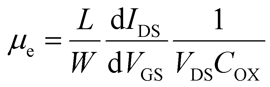 | (1) |
2.7 DFT calculations
The quantum mechanical calculations were performed using DFT as implemented in the Vienna ab initio Simulation Package (VASP).31,32 The generalised-gradient approximation (GGA) was employed with the Perdew–Burke–Ernzerhof (PBE)33 exchange–correlation functional and projector-augmented wave (PAW)34 method to define the ion–electron interaction. An energy cut-off of 400 eV was used, with a k-point mesh of 5 × 5 × 1 for the geometry optimizations and 1 × 1 × 1 for the ab initio molecular dynamic (AIMD) simulations to sample the Brillouin zone. vdW forces were accounted for by the Grimme DFT-D3 approach.35 The AIMD simulations were performed at 298 K with a time step of 0.5 fs for up to 3.8 ps.The SnO2(110) surface was cleaved from bulk SnO2 with cell dimensions of 4.83 × 4.83 × 3.24 Å, which agrees with a previous DFT study.36 The (110) facet was selected as it is the most thermodynamically stable surface.37,38 A [4 × 2] model was used, having lattice parameters of a = 12.97 Å and b = 13.67 Å. A vacuum spacer of 20 Å was added in the z-direction to minimize interactions between adjacent cells after applying periodic boundary conditions. To represent the defect surface, one of the topmost surface O atoms was removed from the stoichiometric surface, creating the SnO2(110)–VO surface. To model the adsorption of octanol on the surface, the adsorbate was initially placed ∼3 Å above each surface in different locations above the surface and in different orientations. The atoms in the bottom surface layer were fixed while all other atoms were allowed to relax until the total energy of the system was converged to 1 × 10⁻⁶ eV and the Hellman–Feynman force on each relaxed atom was less than 0.01 eV Å−1. The binding energies were calculated as BE = (Eoctanol+surface − Esurface − Eoctanol), where Eoctanol+surface, Esurface, and Eoctanol are the total energies of the adsorbed system, the isolated surface and the isolated octanol, respectively. The octanol molecule was optimised in a 30 × 30 × 30 Å3 sized cell using a k-point mesh of 1 × 1 × 1.
3. Results and discussion
3.1. Formation of SnO2 nanosheets by LM method
Ultra-thin tin oxide nanosheets were synthesised by the LM process as illustrated in Fig. 1(a). Briefly, the initial step involves heating the tin metal to its liquid phase, followed by contacting with a flat preheated SiO2 substrate. Since the heating process took place under atmospheric conditions, it resulted in the formation of interfacial tin oxide layers over the tin metal. The attachment between the tin metal and the interfacially formed tin oxides is relatively weak. In comparison, vdW interactions between the solid substrate and the interfacial oxide layer are stronger, enabling the tin oxide nanosheets to be detached from the tin metal surface and subsequently forming ultra-thin layers on a solid substrate.20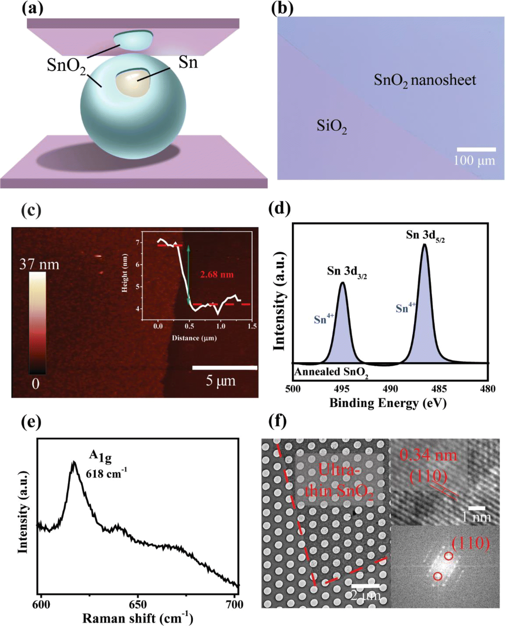 | ||
| Fig. 1 High-quality SnO2 nanosheets by the LM touch printing method. (a) Schematic illustration of ultrathin SnO2 nanosheets forming on the SiO2 substrate. (b) Optical image of obtained SnO2 nanosheet on SiO2 (300 nm)/Si substrate. (c) AFM image of a SnO2 nanosheet with the corresponding step height profile (top right inset). (d) XPS spectrum in the Sn 3d region of the SnO2 nanosheet. (e) Raman spectrum of a SnO2 nanosheet. (f) TEM (left), HRTEM (top right), and the corresponding FFT (bottom right) images of the SnO2 nanosheet. | ||
The obtained pristine SnOx nanosheets were examined under an optical microscope shown in Fig. S1(a).† The different reflection colour displayed under the optical microscopy depicts the successful delamination of tin oxide nanosheets (blue colour), which have been transferred onto SiO2 substrates (purple colour). This finding, in conjunction with previous reports in the literature,21,28,39–41 suggests the feasibility of exfoliating ultra-thin tin oxide nanosheets by LM. Large-scale fabrication with lateral dimensions reaching millimetre scales is also achievable (Fig. S1(b)†), demonstrating the potential for integrating 2D materials into semiconductor manufacturing.24,42–46 Further characterisation by XPS reveals that the as-synthesised SnOx nanosheets contain a mixture of Sn2+ and Sn4+ oxidation states, indicating a degree of chemical inhomogeneity in the structure (Fig. S2†).
Thermal annealing was then applied to treat the as-synthesised SnOx nanosheets. After being heated at 450 °C for 15 minutes in the air, the sample was re-examined under the optical microscope. Its colour became lighter as depicted in Fig. 1(b). The high-resolution morphology of the annealed samples is visualised through AFM in Fig. 1(c) and Fig. S3,† showing a smooth and flat nanosheet with a thickness of 2.68 ± 0.34 nm. The XPS spectra of Sn 3d in Fig. 1d show Sn 3d3/2 peaking at the binding energies of 494.9 eV and Sn 3d5/2 at 486.9 eV. The deconvolution of these two peaks reveals dominating Sn4+ chemical characteristics in the annealed samples. Raman spectroscopy was also employed to characterise the annealed SnOx nanosheets (Fig. 1(e)). The peak at 618 cm−1 presents the A1g mode of the tetragonal rutile structure of SnO2 crystals with the existence of bridging oxygen vacancies.47 TEM images of annealed SnOx in Fig. 1(f) reveal a homogeneous appearance with a d-spacing of 0.34 nm, corresponding to the (110) index of SnO2 crystals, as corroborated by the fast Fourier transforms (FFT) analysis. It was confirmed that after the annealing process, SnOx has been transited into SnO2. Therefore, the obtained annealed SnOx nanosheets are noted as SnO2 in the following studies.
3.2. Electronic performance of solvent-treated SnO2 nanosheets
The high-quality and large-scale SnO2 nanosheets generated on silica substrates allow to fabricate electronic devices conveniently. As illustrated in Fig. 2(a), SnO2-based two terminal devices/FETs were constructed. The solvent molecules were then deposited onto the surface of SnO2 afterwards. The electronic behaviours of the SnO2 before and after the solvent coating were assessed and compared.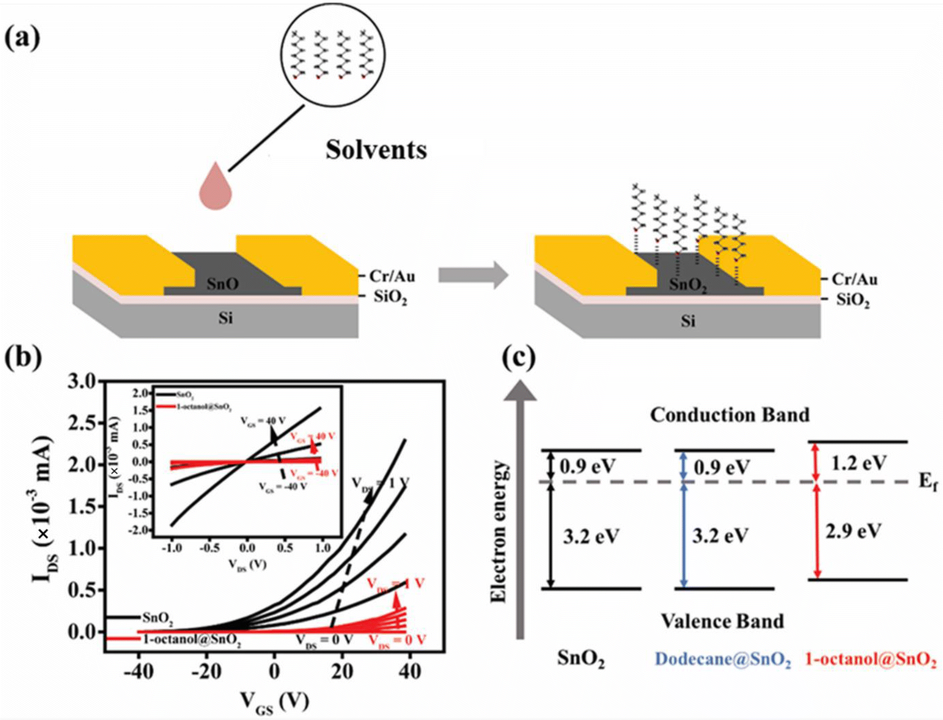 | ||
| Fig. 2 Electronic performance of solvent-treated SnO2 surface. (a) A schematic illustration of coating solvents onto SnO2-based FET electronic devices device. (b) Transfer curves of FET devices based on annealed SnO2 nanosheets before (black) and after (red) applying 1-octanol with VDS ranging from 0 to 1 V. The inset in (b) shows the output curves of the FET device based on annealed SnO2 nanosheets before (black) and after (red) applying 1-octanol with varying VGS from −40 to 40 V. (c) Simplified band diagrams of SnO2, 1-octanol@ SnO2, and dodecane@ SnO2, respectively. | ||
The current–voltage (I–V) curves of SnO2-based devices were tested initially. When applying dodecane onto SnO2, there was a negligible change in I–V behaviour (Fig. S4†). However, when the surface of SnO2 was exposed to 1-octanol, unexpectedly higher electric resistance was displayed on 1-octanol@SnO2 devices compared to SnO2 devices (Fig. S5†). To investigate this further, back-gated FET devices were constructed. The SnO2 nanosheet-based transistor exhibited exceptional electronic performance, attributed to fast electron mobility and high conductivity of LM-derived 2D SnO2.23 The output curves (IDSvs. VDS) and transfer curves (IDSvs. VGS) plotted in Fig. 2(b), respectively, confirmed the n-type semiconducting behaviour of SnO2 nanosheets48 with electron mobility μe of 2.2 cm2 V−1 s−1. Upon applying 1-octanol onto SnO2, it is pronounced to see the significant alterations in the FET device performance. Both IDS–VDS and IDS–VGS profiles of the devices exhibited a significant reduction in the drain current. At VGS = 40 V and VDS = 1 V, IDS decreased from 1.56 μA to 0.08 μA as shown in Fig. 2(b) insert, indicating a huge drop in μe. Although it retained n-type semiconducting behaviour after 1-octanol coated on the SnO2 surface, μe of 1-octanol@SnO2 FET was calculated to be 0.3 cm2 V−1 s−1. An 86% reduction in electron mobility suggests a compromised performance when the SnO2 surface is covered by 1-octanol molecules. The on/off ratio of the device was also decreased from 2.45 × 10³ to 8.93 × 10², which is consistent with observation on the I–V characteristics.
It is known that the electron mobility of the n-type semiconductor is influenced by the position of the Fermi level (Ef) to the conductive band.46 To construct the band diagram, Tauc plots of these samples were extracted from UV-vis absorption spectra first. By extrapolating the linear part, the optical bandgaps for all the samples are found to remain at ∼4.1 eV (Fig. S6(a)†). XPS valence band analysis (VB-XPS) was performed as well. The Fermi level positions of these samples relative to their valence band edge were determined by extrapolating the onset of the leading edge of the VB-XPS (Fig. S6(b)†). They are observed to be 3.2 eV for both SnO2 nanosheets and the dodecane-treated ones, while 2.9 eV for the 1-octanol-treated SnO2 nanosheets. Accordingly, the simplified electronic band structures of these three samples are provided in Fig. 2(c). Notably, the Fermi level of SnO2 shifts away from its conduction band when 1-octanol was capped onto the surface, enlarging the barrier for electrons in the valence band to transition into the conduction band.49 On the other hand, it is possible that the interaction between 1-octanol and the SnO2 surface results in distortion of the SnO2 crystal lattice and reduction of overall electron concentrations.19 As a result, the electronic performance of SnO2-based devices is suppressed.
3.3 Surface states of solvent-treated SnO2 nanosheets
It is evident that the electronic properties of SnO2 were sensitive to surface. To probe the surface chemistry of the aforementioned organic molecule treated SnO2, XPS as a surface-sensitive technique, was deployed.50 The high-resolution survey of the Sn 3d in Fig. 3(a) showed that the Sn 3d5/2 peak of the SnO2 was at 486.9 eV initially. After the deposition of dodecane onto SnO2 nanosheets, a subtle shift of 0.1 eV in the Sn 3d5/2 peak occurred. As for 1-octanol-treated SnO2, a more pronounced shift toward a low binding energy in the Sn 3d5/2 peak, to 486.6 eV, was observed. Such a shift suggests an increase in the electron density around Sn atoms, resulting from the change in Sn atom binding states.51 The normalised carbon-to-tin (C![[thin space (1/6-em)]](https://www.rsc.org/images/entities/char_2009.gif) :Sn) ratios are 0.24 and 0.26 for dodecane@SnO2 and 1-octanol@SnO2 (Fig. 3(b)), respectively, suggesting ∼0.02 dodecane molecule per Sn atom and ∼0.031-octanol molecules per Sn atom on the SnO2 surface. Notably, with similar coverage on SnO2, 1-octanol, containing the OH group, displayed much stronger interactions with Sn atoms than dodecane, consequently altering the electronic properties of SnO2.52 We also conducted tests with other alkane solvents including decane and hexadecane, which showed no impact on the Sn 3d5/2 peak energy (Fig. 3(b)). As for other primary alcohols including ethanol and 1-pentanol, interestingly, ethanol has little impact on I–V characteristics (see Fig. S7†) and the Sn 3d5/2 peak energy of SnO2. While similar to 1-octanol, 1-pentanol made the electric resistance of SnO2 increase (see Fig. S8†), and the Sn 3d5/2 peak shifted 0.3 eV to a low energy side. The results herein signify the roles of both the alkyl chain and the OH group in interacting with the SnO2 surface. It is considered that the OH group with unpaired electrons on its oxygen atom is capable of binding with Sn atoms and the alkyl chain can facilitate such interactions via physical absorption,19 collectively suppressing the electronic mobility and conductivity of SnO2. The observed synergy impact of alcohol molecules on SnO2 is regarded as the doping effect. Positive dipoles of the OH group are likely to induce the depletion of charge carriers in the SnO2 conduction band, lowering charge mobilities and densities.53 Meanwhile, the physisorbed long alkyl chain with a wide bandgap hinders efficient charge transfer.54 Therefore, SnO2 treated by 1-octanol and 1-pentanol exhibited pronounced Sn 3d5/2 peak energy shift as well as a significant decrease in the electronic mobility and conductivity.
:Sn) ratios are 0.24 and 0.26 for dodecane@SnO2 and 1-octanol@SnO2 (Fig. 3(b)), respectively, suggesting ∼0.02 dodecane molecule per Sn atom and ∼0.031-octanol molecules per Sn atom on the SnO2 surface. Notably, with similar coverage on SnO2, 1-octanol, containing the OH group, displayed much stronger interactions with Sn atoms than dodecane, consequently altering the electronic properties of SnO2.52 We also conducted tests with other alkane solvents including decane and hexadecane, which showed no impact on the Sn 3d5/2 peak energy (Fig. 3(b)). As for other primary alcohols including ethanol and 1-pentanol, interestingly, ethanol has little impact on I–V characteristics (see Fig. S7†) and the Sn 3d5/2 peak energy of SnO2. While similar to 1-octanol, 1-pentanol made the electric resistance of SnO2 increase (see Fig. S8†), and the Sn 3d5/2 peak shifted 0.3 eV to a low energy side. The results herein signify the roles of both the alkyl chain and the OH group in interacting with the SnO2 surface. It is considered that the OH group with unpaired electrons on its oxygen atom is capable of binding with Sn atoms and the alkyl chain can facilitate such interactions via physical absorption,19 collectively suppressing the electronic mobility and conductivity of SnO2. The observed synergy impact of alcohol molecules on SnO2 is regarded as the doping effect. Positive dipoles of the OH group are likely to induce the depletion of charge carriers in the SnO2 conduction band, lowering charge mobilities and densities.53 Meanwhile, the physisorbed long alkyl chain with a wide bandgap hinders efficient charge transfer.54 Therefore, SnO2 treated by 1-octanol and 1-pentanol exhibited pronounced Sn 3d5/2 peak energy shift as well as a significant decrease in the electronic mobility and conductivity.
 | ||
| Fig. 3 Surface characterisation of solvent-treated SnO2. (a) XPS spectra in the Sn 3d5/2 region of the SnO2 nanosheet, where the black represents pristine SnO2, the blue represents dodecane@SnO2, and the red represents 1-octanol@SnO2. (b) Normalised C:Sn ratios from SnO2 treated by alkanes including decane (C10H22), dodecane (C12H26), and hexadecane (C16H34) as well as alcohols including ethanol (C2H6O), 1-pentanol (C5H12O) and 1-octanol (C8H18O). Note that the carbon-to-tin ratio of solvents@SnO2 is normalised by the carbon-to-tin ratio obtained on the SnO2 surface to provide a semi-quantitative estimation. (c) The binding energy of Sn 3d5/2 in indicated solvent-treated SnO2. | ||
As for alkane molecules, unlike previously reported work on layered 2D materials, our results indicated that the physical absorption of these hydrocarbons has little impact on the Sn binding energy and SnO2 electronic behaviours. Also, the influence of solvent volatility, which is reduced along with increased hydrocarbon chains, cannot be excluded. Compared to 1-octanol and 1-pentanol, ethanol is more volatile and readily evaporates thus its contact with SnO2 is relatively insufficient under the incubation condition with negligible influence.
3.4. Mechanism of 1-octanol interacting with SnO2 surface
Elucidation of the binding mechanism between 1-octanol and SnO2 nanosheets is expanded upon through the utilisation of DFT calculations and AIMD simulations, as presented in Fig. 4 and Fig. S9.† Both the pristine Sn surface (SnO2) and the surface with oxygen vacancies (SnO2–VO) were examined. Interestingly, 1-octanol was observed to preferentially adsorb dissociatively on both surfaces as follows:| C8H17OH(g) → C8H17O(ads) + H(ads) | (2) |
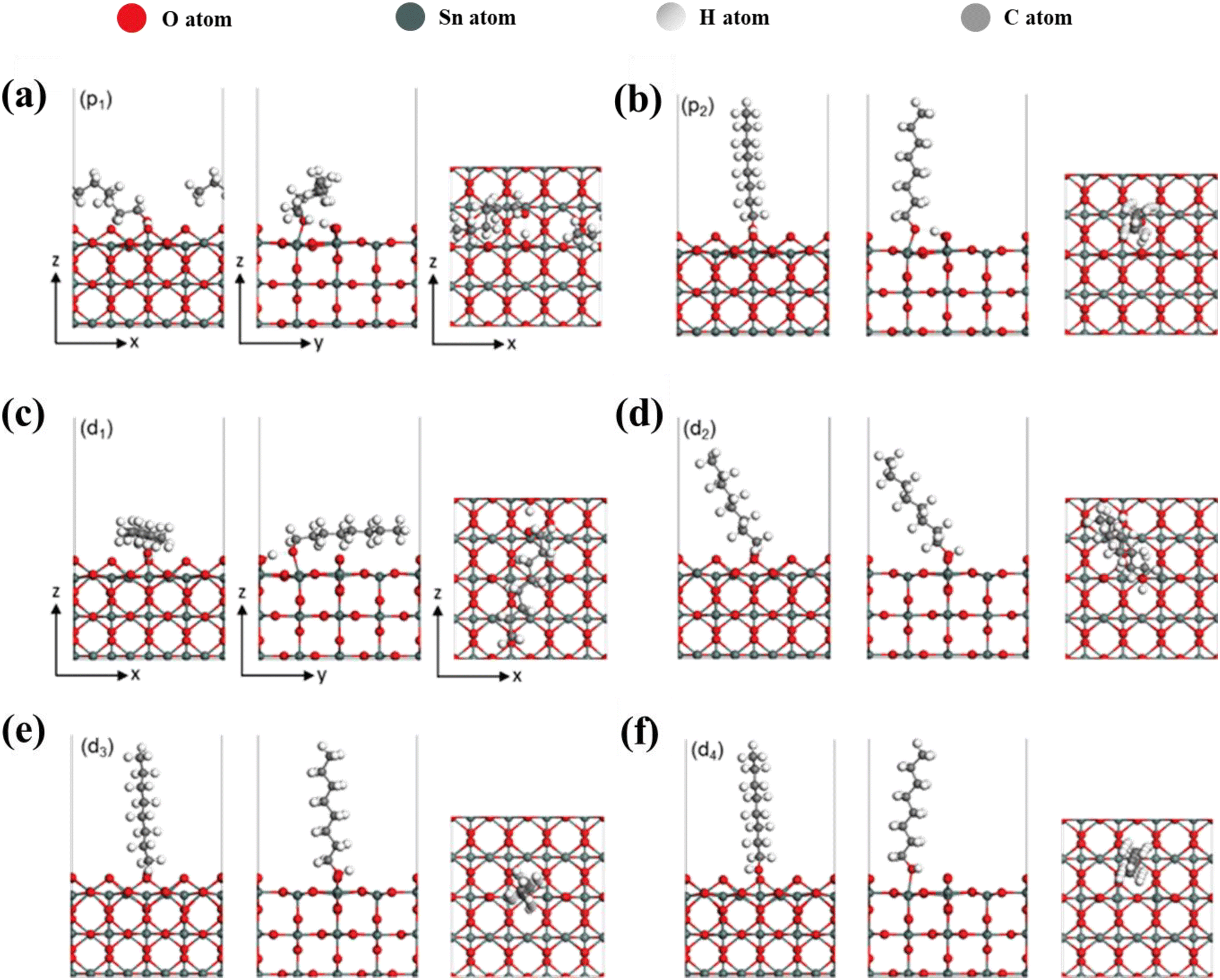 | ||
| Fig. 4 Top and side views of stable configurations of 1-octanol interacting with SnO2 surface via DFT modelling. (a and b) 1-octanol adsorbed on the stoichiometric SnO2(110) surface. (c–f) 1-octanol adsorbed on the SnO2(110)–VO surface. | ||
The specific orientations of the 1-octanol molecule on each surface are illustrated in Fig. 4 and Table S1† summarises the binding energy (BE, eV), along with crucial bond distances (d, Å), pertaining to the stable configurations of 1-octanol adsorbed onto the SnO2 and SnO2–VO surfaces. In the case of the SnO2 surface (Fig. 4(a and b)), there are two stable orientations with BE of −1.62 eV for p1 and −1.54 eV for p2. For both structures, 1-octanol chemisorbs on the surface by its O atom binding to a surface Sn atom. This process causes the O–H bond to break, resulting H atom bonding to a neighbouring surface O atom on SnO2. The binding is also stabilised via formation of a hydrogen bond between the H and O atoms of the octanol. With a lower BE, structure p1 is regarded as more stable than structure p2 as the enhanced binding is achieved due to the alkyl chain being flat across the surface. For the SnO2–VO surface, four stable orientations were found with all structures chemisorbed having BE values of −2.24, −1.21, −1.19, and −1.07 eV, respectively. Similar to the p1 structure on the SnO2, the most stable structure, d1, binds to the SnO2–VO surface by breaking the O–H bond in the hydroxyl group and forming the O–Sn bond. The alkyl chain is also found to be flat along the surface. The binding is stronger than that in p1. This is likely due to the different conformation of the hydrocarbon chain, which sits closer to the surface in d2, enhancing its interaction with the surface. For d2, d3 and d4, the OH bond remains intact, with 1-octanol adsorbing associatively. In d2 and d3, the O atom of 1-octanol bonds to a Sn atom at the defect site while in d4, it bonds to a surface Sn atom. Clearly, the orientation of the alkyl chain is vital to the binding strength. In comparison with d1, d4, with a much lower BE, is less stable as its alkyl chain is oriented almost perpendicular to the surface.
Overall, the DFT findings are consistent with our experimental results, substantiating that the stable chemisorption between 1-octanol and the SnO2 surface causes the distribution change of electron density on SnO2. While it is considered that the formation of a bond between octanol and the SnO2 is essential for such a change, the conformation of the alkyl chain also matters to the binding stability. A horizontal alignment of the alkyl chain is much more favourable than a vertical alignment for enhancing the binding. Therefore, it is reasonable to see a subtle impact of ethanol onto the SnO2 surface. Without stabilising from a long alkyl chain, the chemisorption of ethanol onto the SnO2 is much weaker. Ethanol can easily dissociate from the surface binding, displaying negligible influence on the electronic properties of SnO2. While, the adsorption of 1-octanol onto SnO2 is considerably stable and strong. Both I–V characterisation and XPS measurements indicated partial restoration of the electronic performance of SnO2 after 1-octanol@SnO2 was treated by ethanol–acetone wash or thermal annealing (Fig. S10†).
4. Conclusion
In summary, we have investigated the impact of alkane solvents and primary alcohols on the electronic performance of LM technique-produced 2D SnO2 nanosheets. Measurements of SnO2-based electronic devices confirmed that the electronic performance of SnO2 remained unchanged when exposed to alkane solvents but dropped significantly when in contact with non-volatile primary alcohols, such as 1-pentanol and 1-octanol. The electron mobility of FET devices fabricated using 1-octanol-modified SnO2 only reached 0.3 cm2 V−1 s−1, far slower than that of SnO2-based FET devices. Combing XPS analysis with DFT modelling, it was ascertained that the adverse effect of non-volatile alcohol-based solvents on SnO2 electronic properties was attributed to the formation of O–Sn bond between the OH group of the solvents and the surface Sn of SnO2, consequently changing the electronic band structure of SnO2 and decreasing its electron mobility and density. Also, the binding stability and strength of alcohol solvents onto the SnO2 surface are associated with the lengths and configuration of hydrocarbon chains in the alcohol molecules, which can potentially interfere with the charge transfer of SnO2. In contrast to ethanol, 1-octanol and 1-pentanol with long alkyl groups tended to strongly absorb on the SnO2 surface with a preferred horizontal configuration of hydrocarbon chains. The experimental and theoretical results were consistent and provided an in-depth understanding of the interactions between organic molecules and unstratified 2D SnO2. The results imply that caution is necessary when using alcohol-based solvents to treat low-dimentional semiconductors, facilitating high-quality 2D MOX fabrication. More importantly, the work provided a strategy to switch the electronic characteristics of SnO2 by doping alcohol molecules having different chain lengths, prompting the novel architecture design of responsive 2D MOX-based optoelectronic devices for sensing and detection applications.Data availability
The data supporting this article have been included as part of the ESI.†Author contributions
X.T.W.: methodology, investigation, writing – original draft, writing – review & editing, C.K.N.: methodology, analysis, investigation, writing – review & editing. P.D.T.: simulation, software, writing – original draft, writing – review & editing. V. K.: writing – original draft, writing – review & editing. N.S.: methodology, writing – review & editing. P.Y.L.: methodology, writing – review & editing. M.J.S.S.: supervision, simulation, writing – review & editing. T.D.: supervision, analysis, writing – review & editing, project administration. L.B.: conceptualisation, investigation, writing – original draft, writing – review & editing, supervision, project administration, funding acquisition.Conflicts of interest
The authors declare no conflict of interest.Acknowledgements
This work was performed in part at the RMIT Micro NanoResearch Facility (MNRF) in the Victorian Node of the Australian National Fabrication Facility (ANFF). The authors would also like to thank the RMIT Microscopy and Microanalysis Facility (RMMF). L. B. and X. W. acknowledge funding support from the Australian Research Council (ARC) DECRA program (DE190101514). T. D. and V. K., acknowledge funding from the ARC DP program (DP220101923). P. L. acknowledges financial support from the ARC DP program (DP200101905). N. S. recognises the support of a McKenzie Postdoctoral Fellowship from the University of Melbourne. P. T. acknowledges RMIT University for their RMIT Research Stipend Scholarship. This research was supported by the Australian Government's National Collaborative Research Infrastructure Strategy (NCRIS), with access to computational resources provided by the National Computational Infrastructure (NCI) Facility and the Pawsey Supercomputing Centre, through the National Computational Merit Allocation Scheme.References
- Y. Gong, et al., Two-Dimensional Hexagonal Boron Nitride for Building Next-Generation Energy-Efficient Devices, ACS Energy Lett., 2021, 6(3), 985–996 CrossRef CAS.
- F. H. Alshammari, M. K. Hota, Z. Wang, H. Al-jawhari and H. N. Alshareef, Atomic-Layer-Deposited SnO2 as Gate Electrode for Indium-Free Transparent Electronics, Adv. Electron. Mater., 2017, 3(9), 1700155 CrossRef.
- K. Mahmood, A. Khalid, F. Nawaz and M. T. Mehran, Low-temperature electrospray-processed SnO2 nanosheets as an electron transporting layer for stable and high-efficiency perovskite solar cells, J. Colloid Interface Sci., 2018, 532, 387–394 CrossRef CAS PubMed.
- R. Zhuang, et al., Solution-grown BiI/BiI(3) van der Waals heterostructures for sensitive X-ray detection, Nat. Commun., 2023, 14(1), 1621 CrossRef CAS PubMed.
- H. Mu, et al., Interface and surface engineering of black phosphorus: a review for optoelectronic and photonic applications, Mater. Futures, 2022, 1(1), 012301 CrossRef CAS.
- W. Wan, Y. Li, X. Ren, Y. Zhao, F. Gao and H. Zhao, 2D SnO2 Nanosheets: Synthesis, Characterisation, Structures, and Excellent Sensing Performance to Ethylene Glycol, Nanomaterials, 2018, 8(2), 112 CrossRef PubMed.
- A. Bhattacharjee, S. Begum, K. Neog and M. Ahmaruzzaman, Facile synthesis of 2D CuO nanoleaves for the catalytic elimination of hazardous and toxic dyes from aqueous phase: a sustainable approach, Environ. Sci. Pollut. Res., 2016, 23(12), 11668–11676 CrossRef CAS PubMed.
- B. Saravanakumar and S.-J. Kim, Growth of 2D ZnO Nanowall for Energy Harvesting Application, J. Phys. Chem. C, 2014, 118(17), 8831–8836 CrossRef CAS.
- P. Aukarasereenont, A. Goff, C. K. Nguyen, C. F. McConville, A. Elbourne, A. Zavabeti and T. Daeneke, Liquid metals: an ideal platform for the synthesis of two-dimensional materials, Chem. Soc. Rev., 2022, 51(4), 1253–1276 RSC.
- X. Hu, K. Liu, Y. Cai, S.-Q. Zang and T. Zhai, 2D Oxides for Electronics and Optoelectronics, Small Sci., 2022, 2(8), 2200008 CrossRef CAS.
- K. Liu, H. Jin, L. Huang, Y. Luo, Z. Zhu, S. Dai, X. Zhuang, Z. Wang, L. Huang and J. Zhou, Puffing ultrathin oxides with nonlayered structures, Sci. Adv., 2022, 8(20), eabn2030 CrossRef CAS PubMed.
- T. Yang, T. T. Song, M. Callsen, J. Zhou, J. W. Chai, Y. P. Feng, S. J. Wang and M. Yang, Atomically Thin 2D Transition Metal Oxides: Structural Reconstruction, Interaction with Substrates, and Potential Applications, Adv. Mater. Interfaces, 2019, 6(1), 1801160 CrossRef.
- L. Yang-Yao, Novel Two-Dimensional Nanomaterial: High Aspect Ratio Titania Nanoflakes, in Titanium Dioxide, ed. Y. Dongfang, IntechOpen, 2018, ch. 2 Search PubMed.
- K. Zuraiqi, C. J. Parker, A. Zavabeti, A. J. Christofferson, S. Maniam, C. F. McConville, K. Chiang and T. Daeneke, Field's Metal Nanodroplets for Creating Phase-Change Materials, ACS Appl. Nano Mater., 2022, 5(5), 5952–5958 CrossRef CAS.
- C. K. Nguyen, A. Mazumder, E. L. H. Mayes, V. Krishnamurthi, A. Zavabeti, B. J. Murdoch, X. Guo, P. Aukarasereenont, A. Dubey and A. Jannat, et al., 2 nm-Thick Indium Oxide Featuring High Mobility, Adv. Mater. Interfaces, 2023, 10(9), 2202036 CrossRef CAS.
- V. Krishnamurthi, T. Ahmed, M. Mohiuddin, A. Zavabeti, N. Pillai, C. F. McConville, N. Mahmood and S. Walia, A Visible-Blind Photodetector and Artificial Optoelectronic Synapse Using Liquid-Metal Exfoliated ZnO Nanosheets, Adv. Opt. Mater., 2021, 9(16), 2100449 CrossRef CAS.
- X. Guo, C. K. Nguyen, A. Mazumder, Y. Wang, N. Syed, E. D. Gaspera, T. Daeneke, S. Walia, S. J. Ippolito and Y. Sabri, et al., Gas sensors based on the oxide skin of liquid indium, Nanoscale, 2023, 15(10), 4972–4981 RSC.
- Y. Xia, L. Xu, S. He, L. Zhou, M. Wang, J. Wang and S. Komarneni, UV-activated WS2/SnO2 2D/0D heterostructures for fast and reversible NO2 gas sensing at room temperature, Sens. Actuators, B, 2022, 364, 131903 CrossRef CAS.
- C. K. Nguyen, P. D. Taylor, A. Zavabeti, H. Alluhaybi, S. Almalki, X. Guo, M. Irfan, M. A. Kobaisi, S. J. Ippolito and M. J. S. Spencer, et al., Instant-in-Air Liquid Metal Printed Ultrathin Tin Oxide for High-Performance Ammonia Sensors, Adv. Funct. Mater., 2023, 2309342 CrossRef.
- A. Zavabeti, J. Z. Ou, B. J. Carey, N. Syed, R. Orrell-Trigg, E. L. H. Mayes, C. Xu, O. Kavehei, A. P. O'Mullane and R. B. Kaner, et al., A liquid metal reaction environment for the room-temperature synthesis of atomically thin metal oxides, Science, 2017, 358(6361), 332–335 CrossRef CAS PubMed.
- T. Yuan, Z. Hu, Y. Zhao, J. Fang, J. Lv, Q. Zhang, Z. Zhuang, L. Gu and S. Hu, Two-Dimensional Amorphous SnOx from Liquid Metal: Mass Production, Phase Transfer, and Electrocatalytic CO2 Reduction toward Formic Acid, Nano Lett., 2020, 20(4), 2916–2922 CrossRef CAS PubMed.
- Y. Masuda, Facet controlled growth mechanism of SnO2 (101) nanosheet assembled film via cold crystallization, Sci. Rep., 2021, 11(1), 11304 CrossRef CAS PubMed.
- N. Syed, C. K. Nguyen, A. Zavabeti, M. X. Low, X. Wei, V. Krishnamurthi, M. Irfan, W. S. L. Lee, N. M. H. Duong and A. T. Nguyen, et al., Vacuum-Free Liquid-Metal-Printed 2D Semiconducting Tin Dioxide: The Effect of Annealing, ACS Appl. Electron. Mater., 2024 DOI:10.1021/acsaelm.3c01842.
- R. S. Datta, N. Syed, A. Zavabeti, A. Jannat, M. Mohiuddin, M. Rokunuzzaman, B. Yue Zhang, M. A. Rahman, P. Atkin and K. A. Messalea, et al., Flexible two-dimensional indium tin oxide fabricated using a liquid metal printing technique, Nat. Electron., 2020, 3(1), 51–58, DOI:10.1038/s41928-019-0353-8.
- V. Paolucci, J. De Santis, L. Lozzi, G. Giorgi and C. Cantalini, Layered amorphous a-SnO2 gas sensors by controlled oxidation of 2D-SnSe2, Sens. Actuators, B, 2022, 350, 130890 CrossRef CAS.
- A. Pálinkás, G. Kálvin, P. Vancsó, K. Kandrai, M. Szendrő, G. Németh, M. Németh, Á. Pekker, J. S. Pap, P. Petrik, K. Kamarás, L. Tapasztó and P. Nemes-Incze, The composition and structure of the ubiquitous hydrocarbon contamination on van der Waals materials, Nat. Commun., 2022, 13(1), 6770 CrossRef PubMed.
- M. Gobbi, E. Orgiu and P. Samorì, When 2D Materials Meet Molecules: Opportunities and Challenges of Hybrid Organic/Inorganic van der Waals Heterostructures, Adv. Mater., 2018, 30(18), 1706103 CrossRef PubMed.
- T. Daeneke, P. Atkin, R. Orrell-Trigg, A. Zavabeti, T. Ahmed, S. Walia, M. Liu, Y. Tachibana, M. Javaid and A. D. Greentree, Wafer-Scale Synthesis of Semiconducting SnO Monolayers from Interfacial Oxide Layers of Metallic Liquid Tin, ACS Nano, 2017, 11(11), 10974–10983 CrossRef CAS PubMed.
- A. Jannat, N. Syed, K. Xu, M. A. Rahman, M. M. M. Talukder, K. A. Messalea, M. Mohiuddin, R. S. Datta, M. W. Khan, T. Alkathiri, B. J. Murdoch, S. Z. Reza, J. Li, T. Daeneke, A. Zavabeti and J. Z. Ou, Printable Single-Unit-Cell-Thick Transparent Zinc-Doped Indium Oxides with Efficient Electron Transport Properties, ACS Nano, 2021, 15(3), 4045–4053 CrossRef CAS PubMed.
- A. Zavabeti, P. Aukarasereenont, H. Tuohey, N. Syed, A. Jannat, A. Elbourne, K. A. Messalea, B. Y. Zhang, B. J. Murdoch, J. G. Partridge, M. Wurdack, D. L. Creedon, J. van Embden, K. Kalantar-Zadeh, S. P. Russo, C. F. McConville and T. Daeneke, High-mobility p-type semiconducting two-dimensional β-TeO2, Nat. Electron., 2021, 4(4), 277–283 CrossRef CAS.
- G. Kresse and J. Furthmüller, Efficient iterative schemes for ab initio total-energy calculations using a plane-wave basis set, Phys. Rev. B: Condens. Matter Mater. Phys., 1996, 54(16), 11169–11186 CrossRef CAS PubMed.
- G. Kresse and J. Furthmüller, Efficiency of ab initio total energy calculations for metals and semiconductors using a plane-wave basis set, Comput. Mater. Sci., 1996, 6(1), 15–50 CrossRef CAS.
- J. P. Perdew, K. Burke and M. Ernzerhof, Generalized Gradient Approximation Made Simple, Phys. Rev. Lett., 1996, 77(18), 3865–3868 CrossRef CAS PubMed.
- P. E. Blochl, Projector Augmented-Wave Method, Phys. Rev. B: Condens. Matter Mater. Phys., 1994, 50(24), 17953–17979 CrossRef PubMed.
- S. Grimme, J. Antony, S. Ehrlich and H. Krieg, A consistent and accurate ab initio parametrization of density functional dispersion correction (DFT-D) for the 94 elements H-Pu, J. Chem. Phys., 2010, 132(15), 154104 CrossRef PubMed.
- Y. Sun, S. Sun, Y. Zheng, Z. Zhang, T. Hou, H. Du and J. Wang, The role of oxygen vacancies on SnO2 in improving formaldehyde competitive adsorption: A DFT study with an experimental verification, Appl. Surf. Sci., 2021, 570, 151110 CrossRef CAS.
- D. Wang, Y. Chen, Z. Liu, L. Li, C. Shi, H. Qin and J. Hu, CO2-sensing properties and mechanism of nano-SnO2 thick-film sensor, Sens. Actuators, B, 2016, 227, 73–84 CrossRef CAS.
- X. Wang, H. Qin, Y. Chen and J. Hu, Sensing Mechanism of SnO2 (110) Surface to CO: Density Functional Theory Calculations, J. Phys. Chem. C, 2014, 118(49), 28548–28561, DOI:10.1021/jp501880r.
- P. Atkin, R. Orrell-Trigg, A. Zavabeti, N. Mahmood, M. R. Field, T. Daeneke, I. S. Cole and K. Kalantar-zadeh, Evolution of 2D tin oxides on the surface of molten tin, Chem. Commun., 2018, 54(17), 2102–2105 RSC.
- C.-H. Huang, H. Chang, T.-Y. Yang, Y.-C. Wang, Y.-L. Chueh and K. Nomura, Artificial Synapse Based on a 2D-SnO2 Memtransistor with Dynamically Tunable Analog Switching for Neuromorphic Computing, ACS Appl. Mater. Interfaces, 2021, 13(44), 52822–52832 CrossRef CAS PubMed.
- D. J. Lee, S. Lee and D. Y. Kim, Sturdy memristive switching characteristics of flexible 2D SnO prepared by liquid-to-solid exfoliation, Ceram. Int., 2021, 47(20), 28437–28443 CrossRef CAS.
- N. Syed, A. Zavabeti, K. A. Messalea, E. Della Gaspera, A. Elbourne, A. Jannat, M. Mohiuddin, B. Y. Zhang, G. Zheng and L. Wang, et al., Wafer-Sized Ultrathin Gallium and Indium Nitride Nanosheets through the Ammonolysis of Liquid Metal Derived Oxides, J. Am. Chem. Soc., 2019, 141(1), 104–108 CrossRef CAS PubMed.
- M. H. Vong, M. Kong, U. Jeong and M. Dickey, Continuous large area oxide printing from liquid metals, SPIE, 2023 Search PubMed.
- Q. Li, J. Lin, T.-Y. Liu, X.-Y. Zhu, W.-H. Yao and J. Liu, Gas-mediated liquid metal printing toward large-scale 2D semiconductors and ultraviolet photodetector, npj 2D Mater. Appl., 2021, 5(1), 36 CrossRef CAS.
- Y. Ye, A. B. Hamlin, J. E. Huddy, M. S. Rahman and W. J. Scheideler, Continuous Liquid Metal Printed 2D Transparent Conductive Oxide Superlattices, Adv. Funct. Mater., 2022, 32(33), 2204235 CrossRef CAS.
- A. B. Hamlin, Y. Ye, J. E. Huddy, M. S. Rahman and W. J. Scheideler, 2D transistors rapidly printed from the crystalline oxide skin of molten indium, npj 2D Mater. Appl., 2022, 6(1), 16 CrossRef CAS.
- L. Z. Liu, T. H. Li, X. L. Wu, J. C. Shen and P. K. Chu, Identification of oxygen vacancy types from Raman spectra of SnO2 nanocrystals, J. Raman Spectrosc., 2012, 43(10), 1423–1426 CrossRef CAS.
- P. Pooja, C. C. Che, S.-H. Zeng, Y. C. Lee, T.-J. Yen and A. Chin, Outstanding High Field-Effect Mobility of 299 cm2 V−1 s−1 by Nitrogen-Doped SnO2 Nanosheet Thin-Film Transistor, Adv. Mater. Technol., 2023, 8(7), 2201521 CrossRef CAS.
- C. K. Nguyen, M. X. Low, A. Zavabeti, B. J. Murdoch, X. Guo, P. Aukarasereenont, A. Mazumder, A. Dubey, A. Jannat and M. A. Rahman, et al., Atomically Thin Antimony-Doped Indium Oxide Nanosheets for Optoelectronics, Adv. Opt. Mater., 2022, 10(20), 2200925 CrossRef CAS.
- E. Ciftyürek, B. Šmíd, Z. Li, V. Matolín and K. Schierbaum, Spectroscopic Understanding of SnO2 and WO3 Metal Oxide Surfaces with Advanced Synchrotron Based; XPS-UPS and Near Ambient Pressure (NAP) XPS Surface Sensitive Techniques for Gas Sensor Applications under Operational Conditions, Sensors, 2019, 19(21), 4737 CrossRef PubMed.
- C. Li, N. Zhang and P. Gao, Lessons learned: how to report XPS data incorrectly about lead-halide perovskites, Mater. Chem. Front., 2023, 7(18), 3797–3802 RSC.
- A. Singh, M. Vats, S. Mohapatra, M. Tomar, A. Chowdhuri and V. Singh, Template-assisted mesoporous SnO2 based gas sensor for NO2 detection at low temperature, J. Porous Mater., 2024, 31(2), 545–555 CrossRef CAS.
- S. Najmaei, et al., Tailoring the Physical Properties of Molybdenum Disulfide Monolayers by Control of Interfacial Chemistry, Nano Lett., 2014, 14(3), 1354–1361 CrossRef CAS PubMed.
- D.-H. Kang, et al., Controllable Nondegenerate p-Type Doping of Tungsten Diselenide by Octadecyltrichlorosilane, ACS Nano, 2015, 9(2), 1099–1107 CrossRef CAS PubMed.
Footnote |
| † Electronic supplementary information (ESI) available. See DOI: https://doi.org/10.1039/d4nr01841a |
| This journal is © The Royal Society of Chemistry 2024 |