
Nanostructure engineering for ferroelectric photovoltaics
Wenzhong
Ji
 ,
Teng
Lu
* and
Yun
Liu
*
,
Teng
Lu
* and
Yun
Liu
*
Research School of Chemistry, The Australian National University, Canberra, ACT 2601, Australia. E-mail: teng.lu@anu.edu.au; yun.liu@anu.edu.au
First published on 17th January 2025
Abstract
Ferroelectric photovoltaics have attracted increasing attention since their discovery in the 1970s, due to their above-bandgap photovoltage and polarized-light-dependent photocurrent. However, their practical applications have been limited by their weak visible light absorption and low photoconductivity. Intrinsic modification of the material, such as bandgap tuning through chemical doping, has proven effective, but usually leads to the degradation of ferroelectricity. Recently, various nanostructures, such as multilayer heterojunctions, nanoparticles, vertically aligned nanocomposites and polar nanoregions, have been developed to enhance photovoltaic performance. These approaches enable the nanoassembly of materials in a lower-dimension manner to optimize the bulk photovoltaic effect whilst effectively preserving or even inducing ferroelectricity. This review highlights the fabrication processes of these emerging ferroelectric nanostructures and evaluates their photovoltaic performance.
 Wenzhong Ji | Wenzhong Ji is a PhD candidate at the Research School of Chemistry (RSC), the Australian National University (ANU). He received his B.E. and M.E. degrees from Northwestern Polytechnical University in 2017 and 2020, respectively. His research focuses on the fabrication of ferroelectric nanostructures by the pulsed laser deposition technique and exploring their potential photoelectric applications. |
 Teng Lu | Teng Lu received his PhD degree from the ANU in 2018. He now works as an Australian Research Council (ARC) Discovery Early Career Researcher Award (DECRA) fellow at the RSC, ANU. His research focuses on the development of polar functional materials for energy conversion and storage, as well as the investigation of their structure–property relationships at different length/time scales and under various external stimuli, such as electric fields, pressure, temperature, and light. |
 Yun Liu | Distinguished Professor Yun Liu holds the prestigious Australian Research Council (ARC) Georgina Sweet Australian Laureate Fellowship and leads the Functional Materials Research Group at the RSC, ANU. Her research focuses on the understanding of the chemistry–structure–property relationships of solids at multiple length scales and their multi-functional coupling effects. Professor Liu pioneers the application of complex materials chemistry to design novel functional materials for use in the electronic technology, energy and environment. She has extensive expertise in ferroelectric, piezoelectric, pyroelectric, dielectric, magnetic, multiferroic, and spintronic materials, and their device applications. |
1. Introduction
Since the discovery of the ferroelectric (FE) photovoltaic (PV) effect in the 1970s,1,2 it has been intensively investigated both theoretically and experimentally.3–5 Unlike traditional semiconductor PVs used for solar cells, which rely on p–n junctions for photo-excited charge carrier separation and transportation, the photovoltaic effect in FE materials is a bulk behavior – the internal electric field throughout the bulk region induced by the electric polarization provides a driving force. Thus, this effect is also called the bulk photovoltaic effect (BPE). One characteristic of the BPE is that the open-circuit photovoltage is far beyond the limitation determined by the material's bandgap (Eg);6 in some cases two to four orders of magnitude higher.7 These BPE materials therefore hold promising potential for third-generation solar cells8 exceeding Shockley–Queisser limitations.9 The BPE also presents polarized-light-dependent photocurrent arising from the coupling between the light polarization and materials’ spontaneous electrical polarization.Coupling between reversible electric polarization and strain, magnetism and light in ferroelectricity would further push photoferroelectric applications beyond the scope of energy conversion.10–12 Additionally, the intrinsic BPE enables simple device design. Therefore, FE materials have been used for applications in various photoelectronic devices13 such as ferroelectric photovoltaic synapses,14,15 solid state memory devices,16,17 and polarized-light-sensitive photodetectors,18 as well as for optically controlled electro-resistance and electrically controlled photovoltage in ferroelectric tunnel junctions.19,20 The combination of BPE and pyroelectricity in FE materials has also been used in temperature/infrared sensors.21,22
However, the main problems of FE materials are their large bandgaps and low electronic conductivity, which lead to limited utilization of visible light and relatively low photocurrent. Many strategies to narrow the bandgap have been proposed, such as ionic doping, but these influence the intrinsic ferroelectricity. In contrast, recently emerging nanostructure design strategies tend to be a more practical solution; that is, they are more controllable and can effectively maintain the ferroelectric features. This review aims to summarize the fabrication processes of these nanostructures and compare their bulk photovoltaic performance. Although many articles have reported the combination of ferroelectric materials with organic trihalide perovskites (OTPs) to achieve high power conversion efficiency, the photovoltaic performance mainly depends on the OTP.23 Therefore, this review only focuses on the structure design of inorganic ferroelectric materials for enhancing or creating BPE.
In the second section of this review, the ballistic and shift current theories will be briefly introduced. In the third section, conventional methods for enhancing BPE through materials modification are summarized before discussing emerging nanocomposites formed by structures of various dimensionalities including multilayers, nanoparticles, and vertically aligned structures and their unique properties in sections 4.1, 4.2 and 4.3. In section 4.4, local polar structures are discussed separately, as these materials can be synthesized from a single raw material in one process, but form a polar nanoregions (PNRs). In the above ferroelectric structures, the materials are synthesized by chemical sol–gel, pulsed electron deposition (PED), pulsed laser deposition (PLD) or RF sputtering methods. In recent years, ferroelectricity in low-dimensional materials has generated much interest, and these materials can form more unique structures through exfoliation and transformation. Section 4.5 will briefly discuss the BPE in these materials. In the final two sections of the review. The photovoltaic performance of the different structures is outlined, and perspectives are provided for future research and technology development.
2. Bulk photovoltaic theory
The BPE has been observed in noncentrosymmetric crystals that belong to 20 point groups, including ferroelectrics and piezoelectrics. The origin of this effect in ferroelectric materials has been attributed to their bulk photovoltaic effect (BPE),24,25 crystal structure,26 domain walls,6,27,28 Schottky barriers29 and depolarization fields.30,31Two main theories have been proposed to explain the BPE in ferroelectrics: the ballistic and shift current theories.32 In the ballistic theory, photoexcited non-thermalized carriers have asymmetric momentum distribution in the conduction band, as shown in Fig. 1. In this theory, the carriers lose energy and descend to the bottom of the band over a free path l0. In the shift current theory, the BPE is quantum-mechanical in nature. Taking into account the non-diagonal elements of the density matrix,33 the BPE is not caused by the carrier movement in the band, but instead by virtual shift R in real space following the carrier band–band transition. These two theories are discussed in further detail below.
 | ||
| Fig. 1 Nonequilibrium carriers’ momentum distribution in (a) centrosymmetric crystals and (b) noncentrosymmetric crystals. Reprinted with permission,34 Copyright 2014, American Physical Society. | ||
2.1 Ballistic theory25,34
When a homogeneous medium without an inversion symmetry center is under uniform illumination, a steady-state current jpv will be generated in short-circuited electrodes; the current value depends on the intensity and polarization of the light. When the electrodes are disconnected, the current jpv will generate an open-circuit voltage Voc, | (1) |
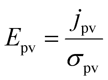 | (2) |
The σpv can also be expressed as
| σpv = eI0αφ(ħω)−1(μτ)pv | (3) |
The tensor properties of the linear BPE current are described by:
| jipv = αGijlejelI0 | (4) |
| jpv = αGI0 | (5) |
 | (6) |
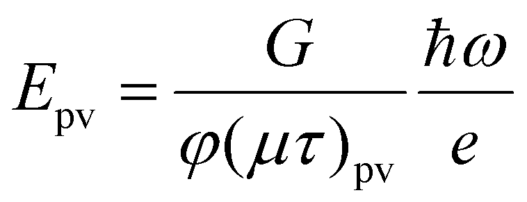
For σpv ≫ σd, the photovoltaic field Epv does not vary with I0, but jpv scales linearly with I0. It is also the case that
| jpv = eI0αφ(ħω)−1ξl0 | (7) |
| l0 = Ge−1ħω(φξ)−1 | (8) |
Here, l0 depends on the asymmetry parameter and the energy of the exciting light. The energy conversion efficiency η for the unit surface is determined by the ratio between the power dissipated in the load, QR = jpv2R', where R' = σpv−1l, and the light absorbed by the unit surface, Qpv = αI0l,
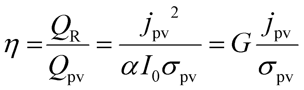 | (9) |
Considering eqns (2) and (9), the conversion efficiency is equal to
| η = GEpv | (10) |
For example, in a (001)-oriented BTO single crystal, G31 = 3 × 10⁻⁹ cm V−1, Epv ≈ 100–200 V cm−1 and η ≈ 10−6–10−7.
2.2 Shift current35,36
In addition to the electron velocity distribution discussed above, there is another shift current that contributes to the BPE stemming from the carrier shift in real space.32,35 This is described by:| jpv = eI0α(ħω)−1R | (11) |
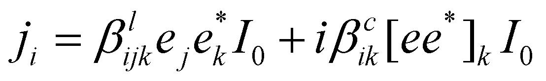 | (12) |
 , where q is the photon wave vector. βlijk is a third-rank tensor and βcik is a second-rank tensor relevant to gyrotropic materials. Based on the two theoretical properties that the shift current does not have photo-Hall behavior and the circular current is purely ballistic, the shift current could be directly observed in the presence of a magnetic field.36
In FE materials, the values of both l0 and R are estimated to be on the order of 10–100 nm.32,37 As l0 represents the free path of the hot photocarriers in space, when the film thickness is less than this value, all photoexcited carriers can be efficiently collected by electrodes before they experience severe recombination. For example, when the thickness l of BTO is close to l0 ≈ 90 nm, η could be significantly increased by five orders of magnitude.34 In terms of shift current, compared to bulk materials, two-dimensional materials can reduce the exciton effect.38 All the above demonstrate the importance and necessity of nanostructure design for achieving high PV performance in FE materials.
3 Intrinsic modification of bulk photovoltaic materials
The power conversion efficiency of ferroelectric thin films is far below the expected value compared with commercial solar cells. The low power conversion efficiency of FE materials (8.1%![[thin space (1/6-em)]](https://www.rsc.org/images/entities/char_2009.gif) 39) is attributed to their large bandgaps, which lead to poor light absorption of the solar spectrum and low electronic conductivity. The short-circuit current (Isc) and open-circuit voltage (Voc) are figures-of-merit to evaluate photovoltaic performance. Tremendous efforts have been made to improve these two parameters, particularly Isc.
39) is attributed to their large bandgaps, which lead to poor light absorption of the solar spectrum and low electronic conductivity. The short-circuit current (Isc) and open-circuit voltage (Voc) are figures-of-merit to evaluate photovoltaic performance. Tremendous efforts have been made to improve these two parameters, particularly Isc.
One strategy to enhance Isc is reducing the materials’ bandgaps to match the solar spectrum. To achieve this, a large number of strategies have been proposed such as chemical doping,40,41 ‘gap-state’ engineering42 and the use of ternary morphotropic phase boundary system43 to introduce intermediate bands. In addition to the traditional perovskite ferroelectric materials LiNbO3,1 BaTiO3 (BTO),34 BiFeO3 (BFO)6,44,45 and Pb(Zr, Ti)O3 (PZT),46 many narrow bandgap ferroelectric materials such as [KNbO3]1−x[BaNi1/2Nb1/2O3−δ]x (KBNNO),47 KBiFe2O5,48 CaMnTi2O6,49 BaFe4O750 and hexagonal manganite and ferrite51–53 have also been explored for BPE in the visible light range. Voc, on the other hand, can be improved by increasing the material thickness, but Isc will deteriorate as a result due to the fact that the free path of the charge carrier contributing to PV is only around tens of nanometers (based on BPE theory, which is discussed above). One method employed to avoid this is taking advantage of the domain wall configuration.6 This is because, based on BPE theory, Voc is inversely proportional to the intrinsic film conductivity (eqn (1)). Note that domain walls are more conductive than the bulk region, thus, when the measurement direction is perpendicular to the domain wall rather than in a parallel configuration, a higher Voc can be obtained.24
Several other methods have also been considered for boosting the BPE. In the FE film fabrication process, the introduction of electronic defects is inevitable. Agarwal54 found that oxygen vacancies could be suppressed by isovalent and aliovalent co-doping on A- and B-sites to reduce the leakage current. Additionally, from a microscopic perspective, the interaction between polarization, lattice and orbital plays an important role in the ferroelectric photovoltaic process. Thus, manipulating the polar order has also been proven to be an effective strategy to enhance BPE, including rhombohedral-to-tetragonal structural transition,55 FE-paraelectric (PE) phase transition56 and polarization gradients in PbTiO357 and KNbO3.58
In all these methods, the improvement in BPE comes from an intrinsic change within the materials. These methods usually require a precise synthesis process, often resulting in the material's physical and chemical properties changing in an unpredictable manner. In addition to the intrinsic properties, many external factors also influence the photovoltaic effect, including the electrode dielectric constant,59 photoexcited electrons from low-work-function electrodes,60 depletion layer thickness29 and upconverter layer.61 For example, when the top electrode is nanoscale in size, photoexcited carriers are collected more efficiently, leading to an enhancement in external quantum efficiency by several orders of magnitude.25,62 Recently, many nanostructures have been designed to combine different materials and create specific geometries for achieving a high BPE. In the following sections, we will present a variety of nanostructures that have been investigated by researchers. It is noteworthy that in addition to the depolarization field (Edp), other coexisting built-in fields, originating from factors such as interfacial junctions, inhomogeneous chemical distribution or strain gradients, may also contribute to the overall photovoltaic effect.
4 Nanostructures
4.1 Multilayers (2–2 type)
Layer-by-layer deposition is the most straightforward method to achieve nano-structure design. In the context of the BPE, multilayer structures have been exploited to change the Schottky barrier at the FE film–metal interface to different junctions by inserting a semiconductor layer. In recent gradient-doped multilayers, additional internal electric fields induced by flexoelectric polarization or a p–n junction further enhance charge carrier separation. For high-quality epitaxial films, the superlattice allows researchers to manipulate the ordering state at an atomic level and tune the materials’ properties, such as their bandgap and dielectric constant, as desired. | (13) |
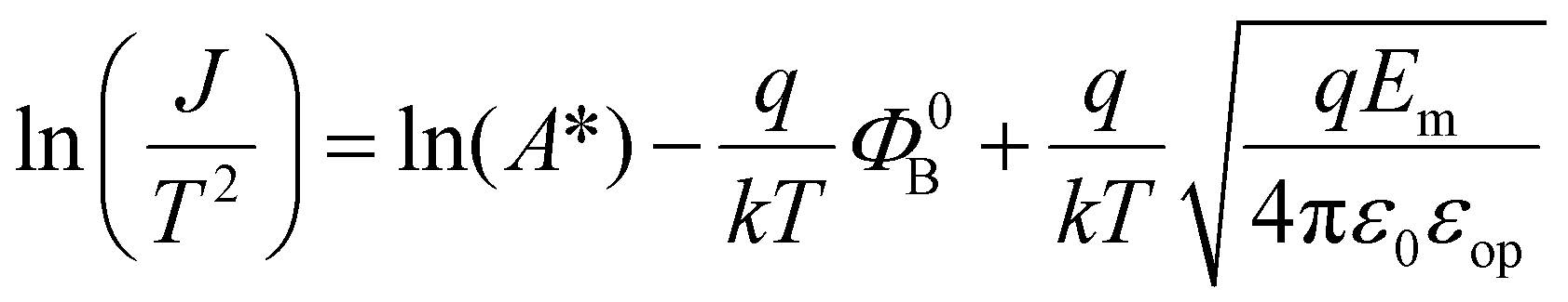 | (14) |
When V = 0, Φ0B is proportional to the slope of the ln(J/T2) − 1/T plot.67,68 The depletion width can be calculated using the equation:
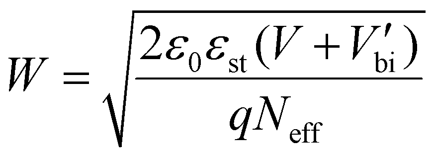 | (15) |
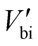 is the built-in potential considering polarization charge contribution, and Neff is the effective charge density. The Schottky barriers in two FE–metal interfaces with opposite directions impede the transport of photoinduced carriers towards the outside circuit. Band structure reconstruction by inserting a semiconductor layer has proven to be an effective way to mediate this process.
For example, Cao et al.67 inserted a Cu2O layer between PZT and Pt (top electrode). The Schottky barrier at the PZT/Pt interface was replaced by a n–n+ junction between PZT/Cu2O, and on the Cu2O/Pt side, the tunneling process dominates the conductance behavior. Due to the aligned depolarization and interfacial electric fields after the interface modification, the short-circuit current density increased from 0.04 to 4.8 mA cm−2 and the power conversion efficiency (PCE) improved from 0.008% to 0.57%, as shown in Fig. 2a. Another metal oxide, ZnO, an n-type semiconductor with high electron mobility, has also been used for the electron transport layer in dye-sensitized solar cells.69 In this work,70 the ZnO layer was chosen to construct an n–n+ junction with BFO, as illustrated in Fig. 2b. The unidirectional driving force at the two interfaces and the additional photoexcited electrons from ZnO simultaneously enhance the photovoltaic performance. Although the authors claimed that the depolarization field had a minor impact on the photovoltaic process, a high energy conversion efficiency of 0.33% was obtained. Wurtzite ZnO also possesses spontaneous polarization induced by strain; this polarization originates from an asymmetric permanent static electric dipole and cannot be altered by an external electric field. When the ZnO layer was exploited to fabricate the PZT/ZnO heterostructure, a polarization-dependent interfacial coupling effect was observed at the p–n junction interface.68 Not only was the PCE improved by 2 orders of magnitude, but it also exhibited a different Voc and Jsc modulation behavior compared to pure PZT, as shown in Fig. 2c and d. Fig. 2e and f illustrate that both the depletion layer width and potential barrier height can be modulated by the polarization direction in PZT. In another study, the same behavior was observed in a Ag/ZnO/BFTO/NSTO structure.71 This continuous tunability of photovoltaic output is suitable for random-access memory applications.72 In addition to metal oxides, n-type reduced graphene oxide has also been used for constructing a p–n junction with p-type BFCO, which improved Jsc by 1000-fold without affecting the Voc or the fill factor (FF).73
 | ||
| Fig. 2 (a) Schematic charge transportation process with and without Cu2O layer. EBi-bottom and EBi-top are Schottky-barrier-induced electric fields at the top and bottom FE–metal interfaces, respectively. EDP is the depolarized field and EPZT/Cu2O is the newly created field. Reprinted with permission,67 Copyright 2012, American Chemical Society. (b) Energy band diagram of the Pt/BFO/ZnO/ITO device. Reprinted with permission,70 Copyright 2014, AIP Publishing. (c) and (d) are the photovoltaic Voc and Jsc hysteresis loops upon applying an external poling voltage sequence. (e) and (f) are schematic illustrations of the depletion layer thickness and the barrier height at the PZT/ZnO interface tuned by different polarization states in PZT. Reprinted with permission,68 Copyright 2016, Springer Nature. | ||
 affects the photovoltaic effect in BFO films.74,75 Therefore, it is worth considering utilizing the distribution of oxygen vacancies to tune the BPE efficiency. Short-range ordered oxygen vacancies can induce incommensurate local structure (Fig. 3a) as reported by Schiemer et al. for Bi1−xCaxFeO3−x/2.76 To take advantage of
  , Zhang77 investigated gradient-doped multilayer structures (Bi1−xCaxFeO3−x/2). The amount of
  in each layer was controlled by the doping concentration, as shown in Fig. 3b. These two stacking geometries had opposite self-polarization direction and photocurrent (Fig. 3c). Due to the strong self-polarization and a gradient
  distribution superposition effect in BFCO-1, the open-circuit voltage and short-circuit current were 2 times and 32 times higher than those of pure BFO, respectively.
 | ||
| Fig. 3 (a) Electron diffraction pattern of Bi0.8Ca0.2FeO2.9 and corresponding structural model. Reprinted with permission,76 Copyright 2009, American Chemical Society. (b) Multilayer Bi1−xCaxFeO3−5x (BCFO) structures with different oxygen vacancy gradient distributions. (c) Photovoltaic I–V curves for three devices. Reprinted with permission,77 Copyright 2020, Elsevier. (d) Energy diagram of Au/multilayer structure (La, Co)-gradient-doped BiFeO3/FTO with an oxygen-vacancy-induced field Ebi-gv. (e) Emerging flexoelectricity in the gradient-doped sample. Reprinted with permission,78 Copyright 2021, American Chemical Society. (f) Illustration of photovoltaic process in the BNO-N2/BNO-O2 structure. (g) Kelvin probe force microscopy (KPFM) characterization of the BNO-N2/BNO-O2 interface. The top panel is the morphology, the middle panel is a cross-sectional surface potential image, and the bottom panel is the surface potential profile of the middle panel. Reprinted with permission,82 Copyright 2021, Royal Society of Chemistry. | ||
The gradient distribution of  in a (La, Co)-gradient-doped BiFeO3 (BFLCO) multilayer was reported by Sun.78 They first conducted XPS and Urbach energy characterization to demonstrate that the
  concentration increases with increasing the amount of the dopant (La). They then fabricated (Bi1−xLaxFe0.975Co0.025O3, x = 0.05, 0.1 and 0.15) multilayer structures. The gradient distribution of
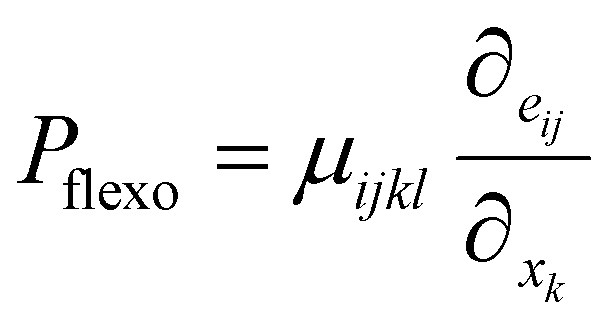
  established an extra built-in electric field, Ebigv, along with an interfacial field, Ebi-s, responsible for photogenerated carrier separation, as illustrated in Fig. 3d. In addition, another flexoelectric field, Eflexo, was created by the strain gradient, considering that the material unit cell volume was modulated by the doping level (Fig. 3e). Eflexo is described by the equation
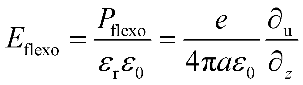 | (16) |
To achieve high BPE, removing centrosymmetry is essential.80 It has been found that material symmetry can be broken by oxygen vacancies.81 Inspired by this idea, Mai82 successfully created a depolarization field in centrosymmetric BiNbO4 deposited by a pulsed electron deposition (PED) technique after annealing in an oxygen-deficient atmosphere (BNO-N2). Later, by combing BNO-N2 with another layer annealed in oxygen (BNO-O2), he constructed the BNO-O2/BNO-N2 homojunction illustrated in Fig. 3f. In this bilayer system, the depolarization field in BNO-N2 and the p–n junction in the BNO-N2/BNO-O2 interface, which was proven by cross-sectional surface potential measurement as shown in Fig. 3g, synergically contributed to the PV performance. Under solar light illumination, the device generated a Voc of 0.85 V and a Jsc of 200 μA cm−2. Another centrosymmetric semiconductor, BiVO4, which has a narrow bandgap of ∼2.6 eV and high organic pollution degradation efficiency under visible-light illumination, is widely used for photocatalysis.83 During its fabrication, bismuth is prone to evaporate at high temperatures. Taking advantage of this property, Shi84 introduced an internal electric field in multilayer BVO with a charge gradient distribution. The structure was fabricated through a multiple-step spin-coating and calcination method. The uneven volatilization of bismuth resulted in the Bi3+ content in the top layer being higher than that in the bottom layer. Consequently, the related gradient compressive stress led to local symmetry breaking and local polarization. Additionally, compared with classical ferroelectric materials, the sample exhibited extraordinary thermal stability.
Among the various FE materials, BFO has been intensively used for BPE due to its relatively narrow bandgap of ∼2.7 eV and high polarization of ∼90 μC cm−2, but it can still only absorb 20% of solar irradiation. The double perovskite Bi2FeCrO6 was predicted to have a lower bandgap and maintain a large remanent polarization.85 Although synthesizing ordered double-perovskite structures is difficult given the thermodynamic process, superlattice (SL) structuring opens a corridor to achieving an atomically well-ordered system. These materials show many exotic properties, such as superexchange interaction86 and polar skyrmions.87 Nechache et al.39 found that ordered and disordered phases coexisted in PLD-synthesized Bi2FeCrO6 (BFCO) films. The ordered phase intensity ratio (R) and domain size (D) are controlled by the deposition temperature and growth time, respectively. These two parameters significantly affect the film bandgap, optical absorption behavior and FE polarization magnitude, as indicated in Fig. 4a–c. At the optimized temperature, by gradually changing the laser repetition during the deposition process, multilayer structures were constructed in which the absorption capability of each layer was superposed, and the bandgap could be reduced to the range of 1.43–2.51 eV. Finally, a recorded high PEC of 8.1% in ferroelectric material was achieved. Regarding this work, a first-principles calculation showed that the photovoltaic improvement is related to efficient electron–hole separation on the Fe and Cr sites,88 and five other promising Bi-based double-perovskite oxides with similar mechanisms were predicted, including (Ti, V), (V, Cu), (Co, Cr), (Mn, Co) and (Fe, V). Based on density functional theory calculations, a narrow bandgap of 1.6 eV can also be obtained in the (BiCrO3)m/(BiFeO3)n superlattice,89 which is correlated to the lattice strain, octahedral distortion and polarization discontinuity at the interface. As ferroelectric polarization is maintained in the system, this structure has potential for highly efficient BPE applications. In another system consisting of PbNiO2 and PbTiO3 nanolayers, theoretical calculations showed a much lower bandgap (1.5 eV) and 43-fold shift-current enhancement.90
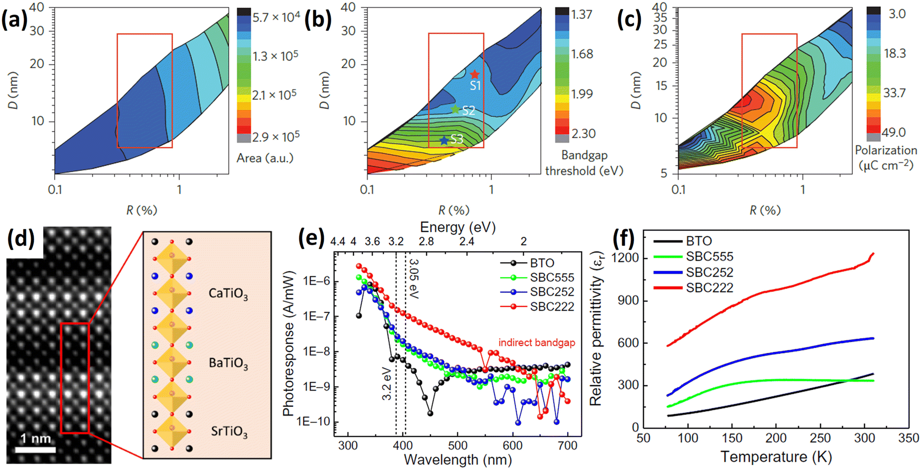 | ||
| Fig. 4 (a–c) Tuneable absorption (a), bandgap (b) and ferroelectric polarization (c) in BFCO by ordering characteristics R and D. Reprinted with permission,39 Copyright 2015, Springer Nature. (d) High-resolution cross-sectional STEM of the STO/BTO/CTO structure. (e) and (f) are the spectral photo-response and temperature-resolved relative permittivity measured at 100 kHz. Reprinted with permission,91 Copyright 2021, The American Association for the Advancement of Science. | ||
Recently, a tricolor SL structure of (SrTiO3)x/(BaTiO3)y/(CaTiO3)z, where x, y and z represent the number of unit cells, was experimentally investigated for BPE91 (Fig. 4d). It could generate a photocurrent three orders higher than a single BaTiO3 layer with similar thickness. By studying the two-color SLs STO/BTO and BTO/CTO, the authors ruled out the influence of the interface and the clipping effect of the substrate. As shown in Fig. 4e and f, the tricolor structure demonstrated a lower bandgap and large dielectric permittivity (εr), which was further affected by the periodicity (x, y, z). In conjunction, the layered arrangement caused subtle displacement of the cations and therefore modified the electronic structure. It has been proven by others that high εr promotes exciton formation, which contributes to the photocurrent.
4.2 FE matrix-nanoparticle composites (0–3 type)
The photovoltaic effect consists of three key steps: photoexcited e–h pair generation, charge carrier separation and transportation. Given that the depolarization field in FE materials is responsible for charge separation and the electrodes for transportation, incorporating narrow bandgap semiconductors or taking advantage of surface plasmon resonance effect to capture more photons will compensate for the weak light absorption of FE materials. Yang et al.92 sputtered a metallic silver target to synthesize elliptical Ag2O nanoparticles (Ag2O-NPs) between two PZT layers, as shown schematically in Fig. 5a. The size was controlled by the sputtering time. The composite showed additional absorption from 350 to 800 nm, and more importantly, the electric polarization within PZT was retained. Although there was a p–n-junction-induced electric field Ebi at the left and right PZT-Ag2O junctions, the e–h pairs generated from the Ag2O NPs were mainly separated by the depolarization field in bulk PZT, as shown in Fig. 5b, and the photocurrent could be tuned via the magnitude of the external poling voltage. Finally, the authors observed an approximate 80-fold improvement of the photocurrent under illumination of a 150 W Xe bulb. The maximum light-conversion efficiency was 0.195% with Jsc = 0.47 mA cm−2, Voc = 0.69 V and FF = 0.6. | ||
| Fig. 5 (a) Schematic structure of PZT/Ag2O-NPs/PZT and the photovoltaic process. (b) Energy band structure between Ag2O-NPs and PZT with the polarization pointing left. Ebi is the electric field at the PZT-Ag2O junction. Reprinted with permission,92 Copyright 2012, John Wiley and Sons. Energy band structure of CFO-PZT composite and the corresponding photoexcited carrier generation, separation and transportation process with (c) and without (d) an external magnetic field. Reprinted with permission,94 Copyright 2016, AIP Publishing. (e) Atomic force microscopy (AFM) image of BWO nanonets grown on STO. (f) TEM image of the heterojunction between Bi2Fe4O9 nanoparticles and BWO. Reprinted with permission,98 Copyright 2024, AIP Publishing. | ||
CoFe2O4 is a member of the magnetic ferrites with a bandgap of around 1.5 eV.93 Pan et al.94 used sol–gel and spin-coating to fabricate a 0–3 type CoFe2O4-Pb(Zr, Ti)O3 (CFO-PZT) composite in which cubic CFO nanoparticles were uniformly distributed in the PZT matrix. Due to the optical bandgap of CFO being smaller than that of PZT, the CFO-PZT composite had a lower bandgap (∼3.48 eV) compared to that of the pure PZT film (∼3.6 eV). In this work, the interfacial barrier between the PZT and CFO impedes photo-induced barriers crossing the interfaces, but the photovoltaic effect can be manipulated by both electric and magnetic fields via a magnetostrictive effect in CFO and piezoelectric effect in PZT (Fig. 5c and d). This work demonstrates that multiferroic composite materials composed of independent ferroelectric and ferromagnetic materials possess strong coupling effects through interfacial stress transfer, and therefore have an impact on the PV effect. The ion implantation technique has been used to fabricate multiferroic materials by introducing transition-metal particles such as Fe95 and Co96 into BTO single crystals. Given the formation of narrow bandgap metal oxides,97 their photovoltaic performance should be influenced, but this has not yet been studied.
When growing ferroelectric Bi2WO6 (BWO) on STO via PLD, Sun98 found that BWO formed a cross-oriented nanonet topography due to the different interfacial free energies and anisotropy of the Aurivillius-type crystals. The morphology is shown in Fig. 5e. Then, mullite-type Bi2Fe4O9 nanoparticles were deposited to create a p–n junction (Fig. 5f). The Jsc and Voc in this structure were four and three orders of magnitude higher than those of pure BWO, respectively. The photocurrent and device resistance could both be modulated by the ferroelectric polarization. Compared with multilayer structures, this nanoparticle/nanonet system has a large interfacial junction area. p-type Sb2Se3 has also been chosen to form a p–n junction with BWO for photovoltaic applications.99
In metal nanoparticles (NPs), the electric field of an incident light beam can polarize surface loosely bound electronic clouds, and this charge separation can be restored by the force from nuclei. Thus, a collective, in-phase conduction electron oscillation occurs, as shown in Fig. 6a. When the frequency of a photon matches the natural frequency of the electron oscillation, surface plasmon resonance (SPR) occurs. This changes the dielectric constant of the material and affects its optical properties.100 This phenomenon has been found in noble metals, metal oxides (WO3−x, MoO3−x and NiO) and metal chalcogenides.101Fig. 6b displays the absorption bands, which are dependent on the material's intrinsic properties. Due to the high electron–hole pair generation rate, hot carrier transfer and reduced charge recombination, SPR fuels photo-related activities such as photocatalysis, photoelectrocatalysis and photodetection.102–106
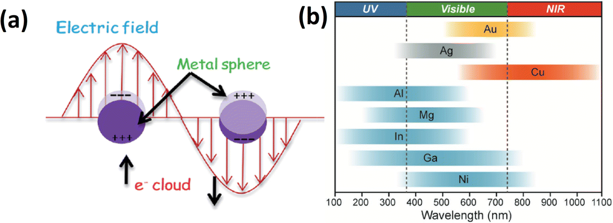 | ||
| Fig. 6 (a) Schematic of surface plasmon resonance. Reprinted with permission,100 Copyright 2016, RSC Publishing. (b) Absorption ranges of different metal nanoparticles. Reprinted with permission,107 Copyright 2018, John Wiley and Sons. | ||
To employ SPR, Maruyama et al.108 fabricated BFO and Ag NP (10–20 nm) thin-film composites via a chemical coating process using colloidal silver and a BiFeO3 metal–organic precursor solution (Fig. 7a). This composite could absorb light in the range of 400–600 nm, and although the absorption edge did not move after the addition of Ag NPs, the absorption capability in the wavelength range of 400–450 nm was strengthened due to the SPR of the Ag NPs. As a result, the photocurrent was enhanced approximately two-fold in the BFO/Au-NPs/BFO and four-fold in the BFO/Au-NPs/BFO/Au-NPs/BFO films relative to that of the pure BFO film, while the photovoltage was not affected by the incorporation of Ag NPs.
 | ||
| Fig. 7 (a) Schematic illustration of BFO/Au-NPs/BFO (BAB) and BFO/Au-NPs/BFO/Au-NPs/BFO (BABAB) structures grown on Pt/TiOx/SiO2/Si substrates. Reprinted with permission,108 Copyright 2016, IOP Publishing on behalf of the Japan Society of Applied Physics. (b) UV-vis absorption of the BLFO and BLFO/AuNPs films. (c) Schematic scattering effect of metal nanoparticles caused light trapping. Reprinted with permission,109 Copyright 2017, Royal Society of Chemistry. (d) Energy band diagram of BFO/ZnO and the photovoltaic mechanism under illumination. (e) Energy band diagram of BFO/Au-NPs/ZnO and emerging pyroelectric polarization charges. (f) UV–vis absorption spectra of BFO, BFO/ZnO and BFO/Au-NPs/ZnO. Reprinted with permission,112 Copyright 2021, Elsevier. (g) HRTEM image of Au nanorods synthesized via a seed-mediated growth method. Reprinted with permission,73 Copyright 2020, Elsevier. (h) Illustration of separation of photoexcited carriers in PZT/metal junctions. hBB and eBB represent UV-light-induced holes and electrons. hsp and esp indicate visible-light-induced holes and electrons. Reprinted with permission,113 Copyright 2014, RSC Pub. | ||
In a report by Li et al.,109 the authors first proved that lanthanum doping could reduce the bandgap of BFO. Subsequently, the visible light absorption of BLFO (550–700 nm) was further enhanced after decorating the surface with Au nanoparticles, as shown in Fig. 7b. Au-PNs 70 nm in diameter were deposited by sputtering. The enhancement was attributed to the light scattering effect increasing the optical path length, as proposed in Fig. 7c, which occurred at large particle size (>40 nm),110 as well as the localized surface plasmon resonance (LSPR) intensifying the optical field. Isc and Voc could also be modulated by an external electric field, which provided evidence of BPE. In bulk form, the BTO-Au nanohybrid ceramic showed an additional absorption peak at 550 nm due to LSPR.111 The photocurrent was seven times that of a pure BTO ceramic, yet the photovoltage had almost the same value (6 V), indicating negligible influence on the polarization.
Band bending has been utilized for enhancing charge separation, as discussed in section 1.2. In a report by Zhang,112 BFO/ZnO exhibits better photoelectric performance compared with BFO, due to the additional driving force Ebi as shown in Fig. 7d. After modifying the heterostructure with Au-NPs, light absorption was detected in a broad spectrum of 360–1000 nm (Fig. 7f). Interestingly, the BFO/Au-NPs/ZnO generated considerable pyroelectric current, which was negligible in the BFO/ZnO sample due to the screening effect (Fig. 7d and e). The authors also investigated the influence of the sputtering time on the photovoltaic effect due to the change of Au-NP grain size. In addition to nanoparticles, Au nanorods were synthesized using a seed-mediated growth method;73 they were then dispersed in ethanol and deposited between BFCO and rCO. As a result, the photovoltage and photocurrent were increased by 12.5% and 66.2%, respectively, compared to the device without Au NRs.73
Although artificial periodic structures or nanoparticle interfaces are generally required for SPR, Zheng et al.113 experimentally and theoretically proved that a rough surface can also introduce the same effect. A 300 nm PZT thin film was deposited on ITO via a sol–gel method, and although the bandgap of PZT is about 3.6 eV, meaning it can only absorb ultraviolet light (UV), the film could generate photocurrent under visible light irradiation after sputtering Ag as the top electrode. Through post-annealing to tune the Schottky barrier height at the PZT/Ag junction, they confirmed that the photocurrent originated from the photogenerated electron–hole pairs in the PZT surface due to enhanced near-fields, as illustrated in the bottom panel of Fig. 7h. This mechanism differs from the hot electrons generated in metal nanoparticles.112
4.3 Vertically aligned structures (1–3 type)
Nanowires are crystalline one-dimensional nanomaterials with high carrier mobility along the growth direction. For example, ferroelectric BiFeO3 nanofibers demonstrated a photocurrent ∼10 times higher in comparison to the thin film.114 In addition, nanowires also have high flexibility, and BaTiO3 nanowire (NW) arrays have demonstrated the harvesting of vibration energy.115 Thus, 1D structures serve as ideal configurations for realizing enhanced photovoltaic performance through polarization and strain coupling via the piezoelectric or flexoelectric effect. In the future, nanowires could be integrated into self-powered wearable devices.Zhang et al.116 grew zinc oxide (ZnO) nanowires on a La-doped bismuth ferrite (BLFO) film. During fabrication, the BLFO was first spin-coated onto FTO, and ZnO seeds were then sputtered onto the film and grew into nanowires in a thermostat oven. Fig. 8a shows a cross-sectional SEM image of the BLFO/ZnO nanowire structure. A finite element analysis (FEA) in COMSOL showed that strain-induced positive piezo-charges accumulated on the BLFO/ZnO interface when the compressive strain was applied. This caused the depletion region to shift to the BLFO side and improved the e–h pair separation efficiency, as indicated in Fig. 8b (from stage 1 to stage 2). After poling the sample, the piezo-photoelectronic effect and the depolarization electric field synergistically enhanced the Voc, Jsc and response speed (Fig. 8c), making it suitable for a future photodetector application.
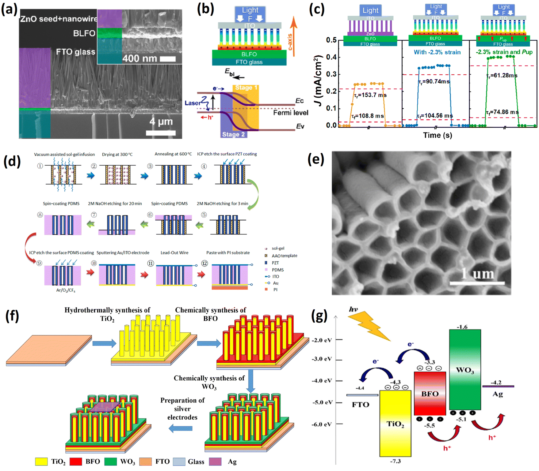 | ||
| Fig. 8 (a) Cross-sectional SEM image of BLFO/ZnO nanowires structure. (b) Energy band diagram of the BLFO/ZnO junction before (stage 1) and after (stage 2) applying compressive force on the top. (c) Photo-response of the device under different strain and polarization conditions. Reprinted with permission,116 Copyright 2020, American Chemical Society. (d) Schematic drawing of the fabrication process of aligned PZT nanowires/PDMS using an AAO template. (e) SEM image of hollow free-standing PZT nanowires after etching of AAO. Reprinted with permission,120 Copyright 2022, American Chemical Society. (f) Illustration of preparation processes of three-dimensional ITO/BFO/WO3. (g) Energy band structure of ITO/BFO/WO3 and transportation process of carriers. Reprinted with permission,122 Copyright 2023, Elsevier. | ||
The flexoelectric effect has been utilized for photovoltaic applications as discussed above.78 The strain gradient induced flexoelectric polarization (Pflexo) is expressed by:
 | (17) |
He et al.122 reported a TiO2/BFO/WO3 core–shell nanowire structure on the FTO substrate synthesized by hydrothermal and chemical liquid methods. The fabrication process is shown schematically in Fig. 8f. Considering the band structure of the three materials, the photoexcited electrons and holes in BFO were first separated by the internal electric field and then transported into the TiO2 and WO3 layers respectively, as shown in Fig. 8g. As previously mentioned, the non-thermalized carriers diffusion length is around tens of nanometres in ferroelectric materials. Therefore, in this device, the large surface area ensured sufficient light absorption, and the two transporting layers efficiently collected e–h pairs and reduced their recombination. Thus, for this specific structure, a high Jsc of 1.14 mA cm−2, Voc of 1.32 V, FF of 58% and PCE of 0.93% were obtained.
In contrast to this complex fabrication processes, self-assembled vertically aligned nanocomposites (SVANs) can be grown in a single process (Fig. 9a). This was first demonstrated for FE materials in 2004 in a perovskite BaTiO3/spinel CoFe2O4 (CFO) system.123 When one 0.65BaTiO3–0.35CoFe2O4 ceramic target was ablated by a pulsed laser to grow a film on STO, in the resultant film, CoFe2O4 nanopillars were embedded in the BaTiO3 matrix. A top-view TEM image is shown in Fig. 9b. This automatic phase separation was attributed to interfacial energy differences. In the following years, SVAN was successfully realized in many multiferroic systems including BaTiO3–CoFe2O4,124 BiFeO3–CoFe2O4,125 PbTiO3–CoFe2O4126 and BiFeO3–NiFe2O4.127 These composites decouple out-of-plane strain from in-plane strain and have large heterointerface areas. Thus, they are ideal platforms for investigating elastic interactions like magnetoelectric coupling.128,129 SVANs provide new degrees of freedom in traditional metal oxide fabrication processes, as well as the integration of the functional properties of two different materials. However, their photovoltaic performance has been little researched. Given that the magnetophotovoltaic effect has been found in a CFO NPs/PZT composite,94 the specific interface configuration of CFO-BTO SVAN should yield better performance.
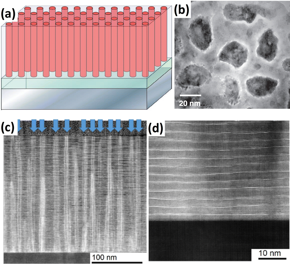 | ||
| Fig. 9 (a) Schematic drawing of a self-assembled vertically aligned nanocomposite on a substrate. (b) TEM top-view image of CFO-BTO SVAN; the dark regions are CFO pillars and the bright area is the BTO matrix. Reprinted with permission,123 Copyright 2004, The American Association for the Advancement of Science. (c) Low-magnification annular-dark field STEM image of PTBNNO. The blue arrows indicate NiO columns. (d) High-resolution high-angle annular dark-field STEM image. Reprinted with permission,130 Copyright 2020, American Chemical Society. | ||
Another self-assembled VAN system was recently found in a (PbTiO3)x(BiNi2/3Nb1/3O3)1−x (PTBNNO) material130 when it was deposited on a single-crystal STO substrate via PLD; two phases coexisted in the film: a nanocolumn NiO phase and a layered (Pb, Nb)-doped bismuth titanate Aurivillius phase. Compared with pure PTO, the layered structure in the SVAN (Fig. 9d) increased the resistance, which is favorable for a high open circuit voltage based on BPE theory.24 In addition, the conductive NiO columns marked by blue arrows in Fig. 9c served as charge transport pathways during the photovoltaic process, which prevented severe degradation of the photocurrent. Consequently, the SVAN thin film exhibited improved photovoltaics compared to pure PbTiO3 and Aurivillius phase films.
4.4 Polar nanoregions (PNRs)
To this point, this review has focused on the simple integration of ferroelectric materials with narrow bandgap semiconductors or noble metals to make full use of their different properties to obtain a high photovoltage and large photocurrent, but the interfaces between the two different materials must be carefully designed to ensure smooth electron transfer. Achieving both strong visible light absorption and the bulk photovoltaic effect within one material is highly desirable. However, narrow bandgap semiconductors usually rely on interfacial junctions for charge carrier separation, as built-in electric fields are inhibited by their high electron conductivity. Inspired by the concept of short-range ordered polar nano-regions (PNRs) in relaxor ferroelectrics, an electric field can be established in nanoscale clusters that arise from local inhomogeneities such as chemical or structural disorder.131 This section of the review explores methods used to introduce ferroelectric behavior into narrow bandgap semiconductors.For the use of the PLD deposition method, many factors must be considered during the deposition of films, such as the laser fluence, pulse frequency, substrate temperature, oxygen pressure, distance between the target and substrate and the post-annealing process. Through delicately control of the deposition conditions, Chakrabartty et al.132 successfully deposited three kinds of films on STO substrates using the same Bi1.4MnO3 target. These were single-phase BiMnO3, BiMn2O5, and mixed crystal phases (Fig. 10a). Compared with the single phases, the mixed phase consisting of ferroelectric BiMnO3 and non-ferroelectric semiconductor BiMn2O5 had a stronger optical absorption and possessed a very high PCE of ∼4.2%. This high performance is attributed to abundant downward band-bending at grain boundaries (GBs). Through conductive AFM and KPFM, the authors confirmed that the photo-charge was mainly generated and transported in the GBs and was not related to topographic artifacts (Fig. 10b and c). The photocurrent can be further manipulated by using different numbers of bipolar voltage pulses, and considering the magnetic properties of BiMnO3, this single-layer perovskite oxide film is expected to have multiferroic properties.
 | ||
| Fig. 10 (a) TEM image of the grain boundary between BMO3 and BiMn2O5. Inset is an illustration of the device for photovoltaic measurement. (b) AFM morphology image. (c) Photocurrent mapping of (b). Reprinted with permission,132 Copyright 2018, Springer Nature. (d) HRTEM image of the mixed phase film with a green circle and red circles indicating Bi4V2O11 and BiVO4, respectively. At the right side are selected area electron diffraction (SAED) patterns of Bi4V2O11 (top) and BiVO4 (bottom). (e) Ferroelectric polarization versus electric field (P–E) hysteresis loop of films of different thicknesses. (f) I–V curve under AM 1.5G (100 mW cm−2) illumination. The top inset is the device configuration for characterizing PV performance. The middle inset is the reverse PV after applying opposite external electric field poling. Reprinted with permission,31 Copyright 2020, Royal Society of Chemistry. (g) Successive magnification of cross-sectional HRTEM image of ZCFLO. (h) I–V curves of ZCFLO films under AM 1.5G light (150 mW cm−2). Reprinted with permission,136 Copyright 2023, John Wiley and Sons. | ||
The photovoltaic effect has also been created in BVO through either strain-induced polarization133 or charge gradient distribution of volatile bismuth.84 In other research, BVO was combined with ferroelectric Bi4V2O11 to form a heterojunction and showed high-performance PV.134 Mai et al.31 found that a local-chemistry-defect could introduce ferroelectric Bi4V2O11 nanoparticles during the synthesis of non-ferroelectric BiVO4 (BVO) film at a high temperature of 600 °C via PLD (Fig. 10d). However, the ferroelectricity was thickness-dependent. In 30 nm thick films, polar nanoparticles were randomly distributed in the matrix, and no overall polarization was detected, but when the thickness was comparable to the particle size of ∼10 nm, the composites showed typical ferroelectricity with remanent polarization 5 μC cm−2, as shown in Fig. 10e. This might be due to the electric boundary condition change and the depolarization field stabilization of the PNRs. In terms of the photovoltaic effect, the narrow bandgap matrix BVO strongly absorbed visible light and generated e–h pairs, and these charge carriers were separated by PNRs. Therefore, the PCE was increased 1000 times compared with that of the BVO ceramic without PNRs. Additionally, the photocurrent was switchable by external electric field poling (Fig. 10f).
Based on the ballistic theory discussed in section 2.1, the photoexcited non-thermalized carriers in noncentrosymmetric crystals lose energy and descend to the conduction band minimum over the free path l0. The value of l0 is estimated to be on the order of 10–100 nm. This is the reason that when the thickness of thin films is close to l0, the ferroelectric photovoltaic will be dramatically enhanced. In other words, high photocurrent in bulk photovoltaics can only be obtained in thin films with a top electrode–FE–bottom electrode configuration, but with a much lower open circuit voltage of ∼1 V. To overcome this limitation, Gao et al.135,136 constructed small-size (5–20 nm) highly crystalline ferroelectric grains in an amorphous thick film, as shown in Fig. 10g. In their previous work,135 Fe3+–Li+ doped ZnO showed an anomalous photovoltaic effect in which the ferroelectricity came from Fe3+–Li+ ionic pairs. Recently, a Cu dopant was added to control the degree of crystallinity and further reduce the bandgap.136 The Zn0.92−xCux(Fe0.04Li0.04)O (ZCFLO) was deposited on a Si substrate via a sol–gel method on top of an LaNiO3 seed layer. After doping, ZCFLO had a much lower bandgap of 1.7 eV compared to 3.4 eV for pure ZnO. Under these circumstances, the amorphous area strongly absorbed light and generated e–h pairs, which were then separated by the ferroelectric nanocrystals. Fig. 10h depicts that the film (x = 0.05) after poling treatment exhibits a record-breaking PCE (14.4%) with an above-bandgap photovoltage (3.75 V), photocurrent (50.3 mA W−1) and FF (83.4%) in an in-plane configuration with interdigital electrode spacing at 300 μm.
4.5 Low-dimensional materials
2D semiconductor materials with reduced dimensionality can be stacked together to form functional devices such as transistors137 and photodetectors.138 More recently, a bulk photovoltaic effect was demonstrated in the 2D materials CuInP2S6,139 MoS2140 and α-In2Se3.30 Apart from the intrinsic ferroelectricity driven by ionic displacement, such as that in the monolayer group-IV monochalcogenides MX (M = Ge, Sn; X = S, Se),141 SnTe,142 GeS nanosheets,143 transition-metal dichalcogenide (MoTe2144), CuInP2S6139,145 and quasi-2D Sn2P2S6,146 the charge redistribution at the interface also gives rise to a ferroelectricity-like behaviour in bilayer graphene/hexagonal boron nitride (h-BN) heterostructure,147 twisted bilayer h-BN148,149 and R-stacking MoS2.140 Given that 2D materials have small effective masses, high carrier mobilities and narrow bandgaps, they are expected to have high photovoltaic performance with both strong light absorption and low recombination rates.150 Although at this stage, these materials cannot be scaled up for energy conversion, the various structure designs extend the realm of the BPE beyond traditional fabricated films and are suitable for minimalized photoelectronic applications.
Zhang et al.151 found that the polar crystal structure is the key factor in achieving high BPE, and therefore, in centrosymmetric bilayer tungsten disulfide (WS2), there is no PV effect, while in WS2, which is non-centrosymmetric but has a non-polar monolayer, the photocurrent is too low to be identified. WS2 multi-wall nanotubes, in which mirror and rotational symmetries are broken, have a non-centrosymmetric and non-polar structure, as illustrated in Fig. 11a, and can even convert 60% of solar energy (photo energies above 1.45 eV based on the indirect bandgap) to electric power. As shown in Fig. 11b, the crossover of the power dependence photocurrent rules out a flexophotovoltaic effect or Schottky barrier contribution and is ascribed to the shift current origin. Later, Sun72 demonstrated the utilization of these multiwall WS2 nanotubes in a photovoltaic random-access memory (PV-RAM) device, which was analogous to resistive random access memory (RRAM).152 As shown in Fig. 11c, in a single nanotube, the photovoltaic Voc and Jsc were programmable by an external poling process. Based on this finding, the authors constructed an artificial vision system on randomly dispersed WS2 nanotubes with multiple functions of sense, memory, computing, and power. Finally, they proposed a van der Waals sliding ferroelectric effect to explain the observed phenomenon, which meant that the electric polarization along the nanotube was created and modulated by the relative deformation of each monolayer, as shown in Fig. 11d.
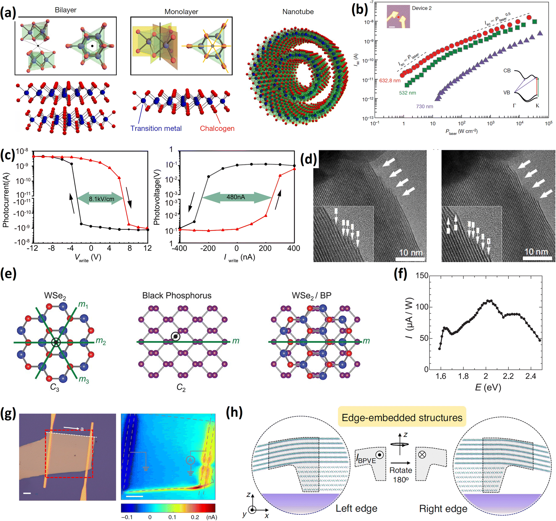 | ||
| Fig. 11 (a) Schematic crystal structure of bilayer and monolayer WS2 and its multi-wall nanotube. The black dots in the bilayer mark the center of the inversion symmetry. The yellow planes and black line at the cross-section in the monolayer indicate the mirror planes and rotation axis. (b) Incident-light-power-dependence of the photocurrent. Reprinted with permission,151 Copyright 2019, Springer Nature. (c) Hysteresis behavior of photovoltaic Jsc and Voc upon external voltage and current sweep. (d) In situ TEM image of layered structure in nanotubes before and after bias. Reprinted with permission,72 Copyright 2022, Springer Nature. (e) Crystal structure of monolayer WSe2, BP and heterointerface of WSe2/BP. The green lines and black dots represent the mirror plane and rotation axes, respectively. (f) Photon-energy-dependence of the photocurrent. Reprinted with permission,153 Copyright 2021, The American Association for the Advancement of Science. (g) Optical microscope image (left) and scanning photocurrent microscopy image (right). Reprinted with permission,155 Copyright 2019, Springer Nature. (h) Cross-sectional schematics of edge-embedded structures and their generation of opposite direction photocurrent. Reprinted with permission,156 Copyright 2023, Springer Nature. | ||
Akamatsu et al.153 reduced the interfacial symmetry by stacking WS2 and BP together. An electronic polarization was thus created parallel to the bilayer mirror plane, due to their different rotational symmetries as shown in Fig. 11e. As a result, a spontaneous photocurrent was observed along this polar direction, but was absent in the perpendicular direction. As shown in Fig. 11f, the photon energy dependence of the photocurrent indicates exciton resonance of WS2 at 1.65 eV and 2.05 eV can enhance the photovoltaic response. This phenomenon and the polarized-light-dependent photocurrent are explained by band hybridization calculations and shift current theory. Recently, an ultra-fast BPE response was demonstrated in a MoS2/BP bilayer taking advantage of the in-plane and out-of-plane dual-polarization.154
In 2019, Wang et al. found a robust photocurrent at certain edges of Weyl semimetal (WTe2) without symmetry constraints, as shown in Fig. 11g.155 Later, Liang reported photocurrent in another interesting geometry called an edge-embedded structure.156 The quasi-1D structure is marked by dashed lines in Fig. 11h. When the two layers were stacked together, the inversion symmetry at the bottom layer edge was broken by vdW coupling. Therefore, this structure showed a typical BPE photocurrent and it was polarized-light-dependent. Interestingly, the current had reversed polarity on opposite side edges. Through first-principles calculations, the authors found that the photo-carriers tended to accumulate at the bottom edge and then were separated by BPE. This specific structure for BPE was proved to be universal in many semiconductor homo- or heterostructures such as ReS2/ReS2, MoS2/MoS2 and WS2/ReS2.
5 Summary
In Table 1, we summarize the photovoltaic performances of all the previously mentioned materials, including their Isc, Voc and PCE values. In multilayers, band-structure engineering has been proven to be an effective strategy to align the internal electric field and achieve high photovoltaic performance. However, considering the large mismatch between the inserted metal oxide and ferroelectric perovskite layers, these devices are generally fabricated via sol–gel methods and contain large amounts of defects, which limit the energy conversion efficiency to below 1%. In gradient-doped films, charge gradient distribution can introduce an additional internal electric field for carrier separation. The pulsed laser deposition technique can produce high-quality epitaxial films. In particular, superlattice structure allows researchers to precisely control the ordering/disordering at the atomic level. By modifying the electronic structure, a narrow bandgap of ∼1.5 eV was experimentally achieved and theoretically predicted in many other ferroelectric thin films. For nanoparticle composites, integrating low-bandgap semiconductors into a ferroelectric matrix can slightly reduce the bandgap. In many reports, the localized surface plasmonic resonance effect of noble metal particles has been utilized for enhancing light absorption at specific visible-range wavelengths. In these 0–3 composites, the particle size has a great impact on photovoltaic performance.| Structure | Fabrication method | Thickness or length (nm) | Remnant polarization Pr (μC cm−2) | Light source | J sc (mA cm−2) | V oc (V) | PCE (%) | Ref. | |
|---|---|---|---|---|---|---|---|---|---|
| Wavelength (nm) | Intensity (mW cm−2) | ||||||||
| a PCE is calculated based on the assumption that the fill factor is 25% for straight I–V curves. | |||||||||
| Transport layers | |||||||||
| ITO/PZT/Cu2O/Pt | Sol–gel | 270 | 25 | AM 1.5G | 100 | 4.8 | 0.42 | 0.57 | 67 |
| ITO/ZnO/BFO/Pt | Radiofrequency (RF) sputtering | 150 | 30 | 435 | 22.3 | 0.34 | 0.2 | 0.33 | 70 |
| Au/PZT/ZnO/ITO | Sol–gel | 130 | 20 | 200–400 | 60 | 0.0424 | 0.681 | 0.012 | 68 |
| Ag/ZnO/BFTO/NSTO | PLD | 200 | 22 | 405 | 200 | 2.2 | 0.15 | 0.045 | 71 |
| Gradient films | |||||||||
| Ag/BCFO/FTO | Sol–gel | 343 | 7 | 405 | 200 | 0.647 | 0.36 | 0.029a | 77 |
| Au/BLCFO-g/FTO | Sol–gel | 270 | 50 | 405 | 50 | 1.73 | — | — | 78 |
| Au/BSFNO-g/FTO | Sol–gel | 210 | 18 | 405 | 50 | 0.08 | 0.49 | 0.0194a | 79 |
| ITO/BNO-N2/BNO-O2/LNO/Y2O3/Si | PED | 300 | 10 | AM 1.5G | 100 | 0.2 | 0.85 | 0.0425a | 82 |
| Au/BVO/Pt | Sol–gel | 200 | — | 450 | 1.63 | 0.38 | 0.4 | 84 | |
| Superlattices | |||||||||
| ITO/BFCO (2 Hz, 8 Hz, 14 Hz)/NSTO | PLD | 285 | 35 | AM 1.5G | 100 | 20.6 | 0.84 | 8.1 | 39 |
| ITO/SBC5555/NSTO | PLD | 200 | — | 405 | — | 0.01103 | 0.058 | — | 91 |
| FE matrix-nanoparticle composites | |||||||||
| Pt/PZT/Ag-8s/Pt | Radiofrequency (RF) sputtering | 400 | 20 | AM 1.5G | 100 | 0.47 | 0.69 | 0.195 | 92 |
| Pt/CFO-PZT/Pt | Sol–gel | 200 | 2.4 | UV | 60 | 0.00384 | 0.164 | 0.00026a | 94 |
| Pt/BFO/BWO/NSTO | PLD | 100 | 0.25 | 405 | 117 | 1.2 | 0.3 | 0.0769a | 98 |
| Pt/Sb2Se3/BWO/NSTO | PLD + vapor transport deposition | 140 | 0.0005 | 405 | 117 | 3.236 | 0.205 | 0.1417a | 99 |
| SPR | |||||||||
| Pt/BABAB/Pt | Sol–gel | 500–550 | 95 (83 K) | 450 | 1 | 0.001 | 0.31 | 0.01 | 108 |
| ITO/AuNPs/BLFO/FTO | Sol–gel | 70 + 476 | 17 | AM 1.5G | 100 | 0.02 | 0.4 | 0.002a | 109 |
| Ag/ZnO/AuNPs/BFO/FTO | Sol–gel | 80 + 50 + 340 | — | 405 | 60 | 0.1719 | 0.34 | 0.0244a | 112 |
| 360 | 26 | 0.0908 | 0.66 | 0.0576a | |||||
| Ag/PZT/ITO | Sol–gel | 300 | 21.15 | AM 1.5G | 100 | 1.32 | 0.82 | 0.42 | 113 |
| Vertically aligned structures | |||||||||
| ITO/ZnO nanowires/BLFO/FTO | Sol–gel | 270 + 6000 | 18 | 405 | 100 | 0.419 | 0.411 | 0.043a | 116 |
| Au/PZT NW/PDMS/ITO | Sol–gel | 5 × 10⁴ | 360 | 20 | 2.26 × 10⁻⁷ | 2.65 | 7.49 × 10⁻⁷a | 120 | |
| ITO/NN-NT/epoxy/Au | Hydrothermal | 4 × 10⁵–5 × 10⁵ | 4.4 | 405 | — | 3.92 × 10⁻⁵ | 0.22 | — | 121 |
| Ag/WO3/BFO/TiO2/FTO | Hydrothermal + sol–gel | 3000 | — | AM 1.5G | 100 | 0.1 | 1.4 | 0.069 | 122 |
| ITO/65PTBNNO/NSTO | PLD | 225 | — | AM 1.5G | 100 | 0.796 | 0.67 | 0.131 | 130 |
| Polar nanoregions | |||||||||
| ITO/Bi–Mn–O/NSTO | PLD | 110 ± 10 | 1.85 (BMO) | AM 1.5G | 100 | 7.03 | 1.48 | 4.2 | 132 |
| ITO/BVO/LNO/YOT/Si | PLD | 10 | 5 | AM 1.5G | 100 | 0.46 | 2.4 | 0.6 | 31 |
| Au/Zn0.88(Fe0.06Li0.06)O/LNO/n+-Si | Sol–gel | 3 × 10⁵ (in-plane) | 1 | 400–830 | 150 | 5.115 | 5.06 | 10.3 | 135 |
| Au/Zn0.87Cu0.05(Fe0.04Li0.04)O/LNO/n+-Si | Sol–gel | 3 × 10⁵ (in-plane) | 2 | AM 1.5G | 150 | 7.545 | 3.75 | 14.4 | 136 |
| 2D materials | |||||||||
| Graphene/CIPS/graphene | Mechanical exfoliation (ME) and transfer | 10 | — | 405 | 300 | 0.8 | 1.65 | 3.67 | 139 |
| Au/graphene/α-In2Se3/graphene/Au | ME and transfer | 18 | — | 520 | 1 × 10⁵ | 0.032 | 0.32 | 0.00256 | 30 |
| Au/WS2 nanotubes (device2)/Au | Chemical vapor transport and ME | 5 × 10³ (D: 90 nm) | — | 632.8 | 1.39 × 10⁷ | 8.56 × 10⁴ | 0.3 | 0.0462a | 151 |
Vertically aligned structures are suitable for fabricating flexible electronic devices by combining FE materials with polymers. In these structures, the piezo- or flexoelectric effect coupled with the photovoltaic makes the photocurrent tunable through strain and electric fields. In the past, complex nanostructures have usually required delicate control of the fabrication process. However, emerging self-assembled vertically aligned nanocomposites and polar nanoregions can be synthesized in a single step through either a physical vapor or a wet chemical method, making them facile and practical for high-performance FE-PV applications. Self-assembled vertically aligned nanocomposites such as those consisting of ferroelectric and magnetoelectric phases have attracted more attention for their ferric properties. In terms of PV applications, the conductive columns can significantly reduce resistance and improve photovoltaic performance. Compared with the above structures, the introduction of local polar nanoregions into narrow bandgap materials is the most promising method to simultaneously achieve high open-circuit voltage and large short-circuit current with a PEC exceeding 1%. More recently, ferroelectricity in low-dimensional materials, particularly two-dimensional van der Waals materials, has been intensively studied due to their various stacking geometries and interfacial configurations. Given that BPE is typically associated with the crystal structure, in low-dimensional materials, the ferroelectricity originates from the charge distribution. This has led to the discovery of many intriguing phenomena and further advancement the development of BPE theory.
6. Perspectives for future research
Improving the collection efficiency of hot photocarriers and enhancing light absorption remain critical challenges in ferroelectric photovoltaics. Addressing these issues requires reducing the scale of ferroelectric materials, providing appropriate charge transport channels and exploring narrow bandgap materials. In narrow bandgap semiconductors, ferroelectric-like behavior has been successfully demonstrated through the formation of polar nanoregions (PNRs). In these systems, light is absorbed by the matrix, and the photo-excited electron–hole pairs are separated by PNRs and then transported through conducive regions. Therefore, in the future, two research directions are expected to receive more attention in efforts to pursue ferroelectric photovoltaics with high power conversion efficiency. The first is low-dimensionalization and integration of ferroelectric materials to maximize the bulk photovoltaic effect. The second involves introducing ferroelectricity into narrow bandgap semiconductors through local chemical deviation, defects or strain engineering.Data availability
All data used in this review were obtained from publicly available literature, as cited in the references. No new data were generated or analysed.Conflicts of interest
There are no conflicts to declare.Acknowledgements
The authors thank the Australian Research Council (ARC) for funding support through the discovery program (DP200100159, DP230100462, DP250101852, DE240100032, FL210100017), and Linkage program (IH24010009).References
- A. M. Glass, D. von der Linde and T. J. Negran, Appl. Phys. Lett., 1974, 25, 233–235 CrossRef.
- W. T. H. Koch, R. Munser, W. Ruppel and P. Wurfel, Solid State Commun., 1975, 17, 847–850 CrossRef.
- Y. Yuan, Z. Xiao, B. Yang and J. Huang, J. Mater. Chem. A, 2014, 2, 6027–6041 RSC.
- P. Lopez-Varo, L. Bertoluzzi, J. Bisquert, M. Alexe, M. Coll, J. Huang, J. A. Jimenez-Tejada, T. Kirchartz, R. Nechache, F. Rosei and Y. Yuan, Phys. Rep., 2016, 653, 1–40 CrossRef.
- Z. Dai and A. M. Rappe, Chem. Phys. Rev., 2023, 4, 011303 CrossRef.
- S. Y. Yang, J. Seidel, S. J. Byrnes, P. Shafer, C.-H. Yang, M. D. Rossell, P. Yu, Y.-H. Chu, J. F. Scott, J. W. Ager, L. W. Martin and R. Ramesh, Nat. Nanotechnol., 2010, 5, 143–147 CrossRef PubMed.
- V. M. Fridkin, Photoferroelectrics, Springer, Berlin, 1979 Search PubMed.
- G. Conibeer, Mater. Today, 2007, 10, 42–50 CrossRef.
- W. Shockley and H. J. Queisser, J. Appl. Phys., 1961, 32, 510–519 CrossRef.
- C. Paillard, X. Bai, I. C. Infante, M. Guennou, G. Geneste, M. Alexe, J. Kreisel and B. Dkhil, Adv. Mater., 2016, 28, 5153–5168 CrossRef CAS PubMed.
- S. Pal, N. V. Sarath, K. S. Priya and P. Murugavel, J. Phys. D: Appl. Phys., 2022, 55, 283001 CrossRef.
- H. Huang and J. F. Scott, Ferroelectric Materials for Energy Applications, John Wiley & Sons, Weinheim, 2018 Search PubMed.
- J. Kreisel, M. Alexe and P. A. Thomas, Nat. Mater., 2012, 11, 260–260 Search PubMed.
- S. Cheng, Z. Fan, J. Rao, L. Hong, Q. Huang, R. Tao, Z. Hou, M. Qin, M. Zeng, X. Lu, G. Zhou, G. Yuan, X. Gao and J. M. Liu, iScience, 2020, 23, 101874 Search PubMed.
- Y. Wang, F. Wang, Z. Wang, J. Wang, J. Yang, Y. Yao, N. Li, M. G. Sendeku, X. Zhan, C. Shan and J. He, Nano Res., 2021, 14, 4328–4335 CrossRef CAS.
- R. Guo, L. You, Y. Zhou, Z. S. Lim, X. Zou, L. Chen, R. Ramesh and J. Wang, Nat. Commun., 2013, 4, 1990 CrossRef PubMed.
- D. Li, D. Zheng, C. Jin, W. Zheng and H. Bai, ACS Appl. Mater. Interfaces, 2018, 10, 19836–19843 CrossRef CAS PubMed.
- Y. Peng, X. Liu, Z. Sun, C. Ji, L. Li, Z. Wu, S. Wang, Y. Yao, M. Hong and J. Luo, Angew. Chem., Int. Ed., 2020, 59, 3933–3937 Search PubMed.
- W. J. Hu, Z. Wang, W. Yu and T. Wu, Nat. Commun., 2016, 7, 10808 CrossRef CAS.
- X. Long, H. Tan, F. Sánchez, I. Fina and J. Fontcuberta, Nat. Commun., 2021, 12, 382 CrossRef CAS PubMed.
- K. Zhao, B. Ouyang and Y. Yang, iScience, 2018, 3, 208–216 CrossRef CAS.
- K. Zhao, B. Ouyang, C. R. Bowen and Y. Yang, Nano Energy, 2020, 77, 105152 CrossRef CAS.
- Y. Liu, S. Wang, Z. Chen and L. Xiao, Sci. China Mater., 2016, 59, 851–866 CrossRef CAS.
- A. Bhatnagar, A. R. Chaudhuri, Y. H. Kim, D. Hesse and M. Alexe, Nat. Commun., 2013, 4, 2835 CrossRef.
- J. E. Spanier, V. M. Fridkin, A. M. Rappe, A. R. Akbashev, A. Polemi, Y. Qi, Z. Gu, S. M. Young, C. J. Hawley, D. Imbrenda, G. Xiao, A. L. Bennett-Jackson and C. L. Johnson, Nat. Photonics, 2016, 10, 611–616 CrossRef.
- L. Kola, D. Murali, S. Pal, B. R. K. Nanda and P. Murugavel, Appl. Phys. Lett., 2019, 114, 183901 CrossRef.
- D. S. Knoche, M. Steimecke, Y. Yun, L. Mühlenbein and A. Bhatnagar, Nat. Commun., 2021, 12, 282 CrossRef PubMed.
- H. Matsuo, Y. Kitanaka, R. Inoue, Y. Noguchi, M. Miyayama, T. Kiguchi and T. J. Konno, Phys. Rev. B, 2016, 94, 214111 CrossRef.
- Z. Tan, L. Hong, Z. Fan, J. Tian, L. Zhang, Y. Jiang, Z. Hou, D. Chen, M. Qin, M. Zeng, J. Gao, X. Lu, G. Zhou, X. Gao and J.-M. Liu, NPG Asia Mater., 2019, 11, 20 CrossRef.
- S. M. Nahid, S. Nam and A. M. van der Zande, ACS Nano, 2024, 18, 14198–14206 CrossRef PubMed.
- H. Mai, T. Lu, Q. Sun, R. G. Elliman, F. Kremer, T. Duong, K. Catchpole, Q. Li, Z. Yi, T. J. Frankcombe and Y. Liu, Mater. Horiz., 2020, 7, 898–904 RSC.
- B. S. I. Sturman and V. M. Fridkin, Photovoltaic and Photorefractive Effects in Noncentrosymmetric Materials, Gordon and Breach, Philadelphia, 1992 Search PubMed.
- S. M. Young and A. M. Rappe, Phys. Rev. Lett., 2012, 109, 116601 CrossRef PubMed.
- A. Zenkevich, Y. Matveyev, K. Maksimova, R. Gaynutdinov, A. Tolstikhina and V. Fridkin, Phys. Rev. B:Condens. Matter Mater. Phys., 2014, 90, 161409 CrossRef.
- V. I. Belinicher, E. L. Ivchenko and B. I. Sturman, Sov. Phys. – JET, 1982, 56, 359–366 Search PubMed.
- A. M. Burger, R. Agarwal, A. Aprelev, E. Schruba, A. Gutierrez-Perez, V. M. Fridkin and J. E. Spanier, Sci. Adv., 2019, 5, eaau5588 CrossRef.
- Z. Gu, D. Imbrenda, A. L. Bennett-Jackson, M. Falmbigl, A. Podpirka, T. C. Parker, D. Shreiber, M. P. Ivill, V. M. Fridkin and J. E. Spanier, Phys. Rev. Lett., 2017, 118, 096601 CrossRef.
- R. Fei, L. Z. Tan and A. M. Rappe, Phys. Rev. B, 2020, 101, 045104 CrossRef CAS.
- R. Nechache, C. Harnagea, S. Li, L. Cardenas, W. Huang, J. Chakrabartty and F. Rosei, Nat. Photonics, 2015, 9, 61–67 CrossRef CAS.
- X. Liu, J. Tu, Y.-W. Fang, G. Xi, H. Li, R. Wu, X. Liu, D. Lu, J. He, J. Zhang, J. Tian and L. Zhang, J. Am. Chem. Soc., 2024, 146, 13934–13948 CrossRef CAS.
- S. Das, S. Ghara, P. Mahadevan, A. Sundaresan, J. Gopalakrishnan and D. D. Sarma, ACS Energy Lett., 2018, 3, 1176–1182 CrossRef CAS.
- H. Matsuo, Y. Noguchi and M. Miyayama, Nat. Commun., 2017, 8, 207 CrossRef.
- L. Wu, A. Podpirka, J. E. Spanier and P. K. Davies, Chem. Mater., 2019, 31, 4184–4194 CrossRef CAS.
- S. Y. Yang, L. W. Martin, S. J. Byrnes, T. E. Conry, S. R. Basu, D. Paran, L. Reichertz, J. Ihlefeld, C. Adamo, A. Melville, Y.-H. Chu, C.-H. Yang, J. L. Musfeldt, D. G. Schlom, J. W. Ager and R. Ramesh, Appl. Phys. Lett., 2009, 95, 062909 CrossRef.
- T. Choi, S. Lee, Y. J. Choi, V. Kiryukhin and S.-W. Cheong, Science, 2009, 324, 63–66 CrossRef CAS PubMed.
- L. Pintilie, I. Vrejoiu, G. Le Rhun and M. Alexe, J. Appl. Phys., 2007, 101, 064109 CrossRef.
- I. Grinberg, D. V. West, M. Torres, G. Gou, D. M. Stein, L. Wu, G. Chen, E. M. Gallo, A. R. Akbashev, P. K. Davies, J. E. Spanier and A. M. Rappe, Nature, 2013, 503, 509–512 CrossRef CAS PubMed.
- G. Zhang, H. Wu, G. Li, Q. Huang, C. Yang, F. Huang, F. Liao and J. Lin, Sci. Rep., 2013, 3, 1265 CrossRef PubMed.
- G. Gou, N. Charles, J. Shi and J. M. Rondinelli, Inorg. Chem., 2017, 56, 11854–11861 CrossRef CAS.
- G. Zhang, J. Hou, M. Zhu, G. Huang, D. Li, Y. Fang and T. Zeng, J. Mater. Chem. C, 2020, 8, 16234–16240 RSC.
- H. Han, S. Song, J. H. Lee, K. J. Kim, G.-W. Kim, T. Park and H. M. Jang, Chem. Mater., 2015, 27, 7425–7432 CrossRef CAS.
- H. Han, D. Kim, K. Chu, J. Park, S. Y. Nam, S. Heo, C. H. Yang and H. M. Jang, ACS Appl. Mater. Interfaces, 2018, 10, 1846–1853 CrossRef CAS.
- H. Han, D. Kim, S. Chae, J. Park, S. Y. Nam, M. Choi, K. Yong, H. J. Kim, J. Son and H. M. Jang, Nanoscale, 2018, 10, 13261–13269 RSC.
- R. Agarwal, Y. Sharma, S. Hong and R. S. Katiyar, J. Phys. D: Appl. Phys., 2018, 51, 275303 CrossRef.
- F. Wang, I. Grinberg and A. M. Rappe, Appl. Phys. Lett., 2014, 104, 152903 CrossRef.
- L. You, F. Zheng, L. Fang, Y. Zhou, L. Z. Tan, Z. Zhang, G. Ma, D. Schmidt, A. Rusydi, L. Wang, L. Chang, A. M. Rappe and J. Wang, Sci. Adv., 2018, eaat3438 CrossRef.
- C. Lin, Z. Zhang, Z. Dai, M. Wu, S. Liu, J. Chen, C. Hua, Y. Lu, F. Zhang, H. Lou, H. Dong, Q. Zeng, J. Ma, X. Pi, D. Zhou, Y. Wu, H. Tian, A. M. Rappe, Z. Ren and G. Han, Nat. Commun., 2023, 14, 2341 CrossRef PubMed.
- Y. Sun, Z. Zhang, X. Fang, Z. Huang, D. Zhou, H. Tian, G. Han and Z. Ren, APL Mater., 2023, 11, 091236 Search PubMed.
- M. Qin, K. Yao and Y. C. Liang, Appl. Phys. Lett., 2009, 95, 022912 CrossRef.
- J. Zhang, X. Su, M. Shen, Z. Dai, L. Zhang, X. He, W. Cheng, M. Cao and G. Zou, Sci. Rep., 2013, 3, 2109 CrossRef PubMed.
- H. Mai, T. Lu, Q. Li, Q. Sun, K. Vu, H. Chen, G. Wang, M. G. Humphrey, F. Kremer, L. Li, R. L. Withers and Y. Liu, ACS Appl. Mater. Interfaces, 2018, 10, 29786–29794 CrossRef.
- M. Alexe and D. Hesse, Nat. Commun., 2011, 2, 256 CrossRef.
- L. Pintilie, C. Dragoi and I. Pintilie, J. Appl. Phys., 2011, 110, 044105 CrossRef.
- A. Abdelsamie, L. You, L. Wang, S. Li, M. Gu and J. Wang, Phys. Rev. Appl., 2022, 17, 024047 CrossRef.
- L. Pintilie and M. Alexe, J. Appl. Phys., 2005, 98, 124103 CrossRef.
- L. Pintilie, I. Vrejoiu, D. Hesse, G. Lerhun and M. Alexe, Phys. Rev. B:Condens. Matter Mater. Phys., 2007, 75, 104103 CrossRef.
- D. Cao, C. Wang, F. Zheng, W. Dong, L. Fang and M. Shen, Nano Lett., 2012, 12, 2803–2809 CrossRef CAS.
- D. Pan, G. Bi, G. Chen, H. Zhang, J. Liu, G. Wang and J. Wan, Sci. Rep., 2016, 6, 22948 CrossRef CAS.
- P. Tiwana, P. Docampo, M. B. Johnston, H. J. Snaith and L. M. Herz, ACS Nano, 2011, 5, 5158–5166 CrossRef CAS PubMed.
- Z. Fan, K. Yao and J. Wang, Appl. Phys. Lett., 2014, 105, 162903 CrossRef.
- J.-M. Yan, K. Wang, Z.-X. Xu, J.-S. Ying, T.-W. Chen, G.-L. Yuan, T. Zhang, H.-W. Zheng, Y. Chai and R.-K. Zheng, J. Mater. Chem. C, 2021, 9, 3287–3294 RSC.
- Y. Sun, S. Xu, Z. Xu, J. Tian, M. Bai, Z. Qi, Y. Niu, H. H. Aung, X. Xiong, J. Han, C. Lu, J. Yin, S. Wang, Q. Chen, R. Tenne, A. Zak and Y. Guo, Nat. Commun., 2022, 13, 5391 Search PubMed.
- H. Renuka, P. Joshna, W. A. Wani, B. H. Venkataraman, K. Ramaswamy and S. Kundu, Mater. Sci. Semicond. Process., 2020, 109, 104937 CrossRef CAS.
- H. T. Yi, T. Choi, S. G. Choi, Y. S. Oh and S. W. Cheong, Adv. Mater., 2011, 23, 3403–3407 CrossRef CAS PubMed.
- T. Yang, J. Wei, Y. Guo, Z. Lv, Z. Xu and Z. Cheng, ACS Appl. Mater. Interfaces, 2019, 11, 23372–23381 CrossRef CAS.
- J. Schiemer, R. Withers, L. Norén, Y. Liu, L. Bourgeois and G. Stewart, Chem. Mater., 2009, 21, 4223–4232 CrossRef CAS.
- Y. Zhang, H. Zheng, X. Wang, H. Li, Y. Wu, Y. Zhang, H. Su and G. Yuan, Ceram. Int., 2020, 46, 10083–10088 CrossRef CAS.
- Z. Sun, J. Wei, T. Yang, Y. Li, Z. Liu, G. Chen, T. Wang, H. Sun and Z. Cheng, ACS Appl. Mater. Interfaces, 2021, 13, 49850–49859 CrossRef CAS PubMed.
- Z. Sun, J. Wei, Y. Li, Z. Liu, M. Xiahou, G. Chen, L. Zhao and Z. Cheng, Inorg. Chem. Front., 2023, 10, 1315–1327 RSC.
- M. Yang and M. Alexe, Nature, 2019, 570, 310–311 CrossRef CAS PubMed.
- W. Dong, D. Cortie, T. Lu, Q. Sun, N. Narayanan, W. Hu, L. Jacob, Q. Li, D. Yu, H. Chen, A. Chen, X. Wei, G. Wang, M. G. Humphrey, T. J. Frankcombe and Y. Liu, Mater. Horiz., 2019, 6, 1717–1725 RSC.
- H. Mai, T. Lu, Q. Sun, J. Langley, N. Cox, F. Kremer, T. Duong, K. Catchpole, H. Chen, Z. Yi, T. J. Frankcombe and Y. Liu, J. Mater. Chem. A, 2021, 9, 13182–13191 RSC.
- A. Malathi, J. Madhavan, M. Ashokkumar and P. Arunachalam, Appl. Catal., A, 2018, 555, 47–74 CrossRef.
- L. Shi, Z. Li, W. Zhao, Z. Wang, Y. Peng, C. Gao, W. Hua, J. Wang, X. Yang, W. Fei and Y. Zhao, Nano Energy, 2023, 114, 108594 CrossRef.
- D. Meng, Y. Xiao, H. He, Y. Liao, H. Zhang, J. Zhai, Z. Chen, L. W. Martin and F. Bai, J. Am. Ceram. Soc., 2019, 102, 5234–5242 CrossRef.
- K. Ueda, H. Tabata and T. Kawai, Science, 1998, 280, 1064–1066 CrossRef PubMed.
- S. Das, Y. L. Tang, Z. Hong, M. A. P. Gonçalves, M. R. Mccarter, C. Klewe, K. X. Nguyen, F. Gómez-Ortiz, P. Shafer, E. Arenholz, V. A. Stoica, S.-L. Hsu, B. Wang, C. Ophus, J. F. Liu, C. T. Nelson, S. Saremi, B. Prasad, A. B. Mei, D. G. Schlom, J. Íñiguez, P. García-Fernández, D. A. Muller, L. Q. Chen, J. Junquera, L. W. Martin and R. Ramesh, Nature, 2019, 568, 368–372 CrossRef PubMed.
- D. Kim, H. Han, J. H. Lee, J. W. Choi, J. C. Grossman, H. M. Jang and D. Kim, Proc. Natl. Acad. Sci. U. S. A., 2018, 115, 6566–6571 CrossRef.
- S. Zhang, H. Y. Xiao, S. M. Peng, G. X. Yang, Z. J. Liu, X. T. Zu, S. Li, D. J. Singh, L. W. Martin and L. Qiao, Phys. Rev. Appl., 2018, 10, 044004 Search PubMed.
- F. Wang, S. M. Young, F. Zheng, I. Grinberg and A. M. Rappe, Nat. Commun., 2016, 7, 10419 Search PubMed.
- Y. Yun, L. Mühlenbein, D. S. Knoche, A. Lotnyk and A. Bhatnagar, Sci. Adv., 2021, 7, eabe4206 Search PubMed.
- X. Yang, X. Su, M. Shen, F. Zheng, Y. Xin, L. Zhang, M. Hua, Y. Chen and V. G. Harris, Adv. Mater., 2012, 24, 1202–1208 Search PubMed.
- D. Sharma and N. Khare, Appl. Phys. Lett., 2014, 105, 032404 CrossRef CAS.
- D.-F. Pan, G.-Y. Chen, G.-F. Bi, H. Zhang, J.-M. Liu, G.-H. Wang and J.-G. Wan, Appl. Phys. Lett., 2016, 108, 222902 CrossRef.
- M. Maksutoğlu, S. Kazan, N. I. Khalitov, V. I. Nuzhdin, R. I. Khaibullin, L. R. Tagirov, V. V. Roddatis, K. E. Prikhodko and F. A. Mikailzade, J. Magn. Magn. Mater., 2015, 373, 103–107 CrossRef.
- M. Algueró, J. Ricote, M. Torres, H. Amorín, A. Alberca, O. Iglesias-Freire, N. Nemes, S. Holgado, M. Cervera, J. Piqueras, A. Asenjo and M. García-Hernández, ACS Appl. Mater. Interfaces, 2014, 6, 1909–1915 CrossRef.
- B. Leedahl, D. A. Zatsepin, D. W. Boukhvalov, R. J. Green, J. A. McLeod, S. S. Kim, E. Z. Kurmaev, I. S. Zhidkov, N. V. Gavrilov, S. O. Cholakh and A. Moewes, J. Appl. Phys., 2014, 115, 053711 CrossRef.
- S. Sun, D. Yang, J. Shen, R. Chen, H. Huang, R. Ti and X. Yin, Appl. Phys. Lett., 2024, 124, 202902 CrossRef.
- S. Sun, D. Yang, W. Han, J. Shen, J. Zhang, H. Huang, G. Wang, W. Zi, X. Li, H. Qi, X. Yin and Y. Lu, Chem. Eng. J., 2024, 486, 150235 CrossRef CAS.
- J. Jana, M. Ganguly and T. Pal, RSC Adv., 2016, 6, 86174–86211 RSC.
- J. Li, Z. Lou and B. Li, Chin. Chem. Lett., 2022, 33, 1154–1168 CrossRef CAS.
- W. Hou and S. B. Cronin, Adv. Funct. Mater., 2013, 23, 1612–1619 CrossRef CAS.
- Y.-L. Huang, W. S. Chang, C. N. Van, H.-J. Liu, K.-A. Tsai, J.-W. Chen, H.-H. Kuo, W.-Y. Tzeng, Y.-C. Chen, C.-L. Wu, C.-W. Luo, Y.-J. Hsu and Y.-H. Chu, Nanoscale, 2016, 8, 15795–15801 RSC.
- J. Zhao, S. Xue, R. Ji, B. Li and J. Li, Chem. Soc. Rev., 2021, 50, 12070–12097 RSC.
- Z. Wang, D. Cao, L. Wen, R. Xu, M. Obergfell, Y. Mi, Z. Zhan, N. Nasori, J. Demsar and Y. Lei, Nat. Commun., 2016, 7, 10348 CrossRef CAS.
- P. Joshna, S. R. Gollu, P. M. P. Raj, B. P. Rao, P. Sahatiya and S. Kundu, Nanotechnology, 2019, 30, 365201 CrossRef CAS PubMed.
- S. Kim, J. M. Kim, J. E. Park and J. M. Nam, Adv. Mater., 2018, 30, 1704528 CrossRef.
- R. Maruyama, W. Sakamoto, I. Yuitoo, T. Takeuchi, K. Hayashi and T. Yogo, Jpn. J. Appl. Phys., 2016, 55, 10TA14 CrossRef.
- F. Z. Li, H. W. Zheng, M. S. Zhu, X. A. Zhang, G. L. Yuan, Z. S. Xie, X. H. Li, G. T. Yue and W. F. Zhang, J. Mater. Chem. C, 2017, 5, 10615–10623 RSC.
- C. Noguez, J. Phys. Chem. C, 2007, 111, 3806–3819 CrossRef CAS.
- R. Su, D. Zhang, M. Wu, F.-t. Li, Y. Liu, Z. Wang, C. Xu, X. Lou, Q. Yu and Y. Yang, J. Alloys Compd., 2019, 785, 584–589 CrossRef CAS.
- Y. Zhang, H. Su, H. Li, Z. Xie, Y. Zhang, Y. Zhou, L. Yang, H. Lu, G. Yuan and H. Zheng, Nano Energy, 2021, 85, 105968 CrossRef CAS.
- F. Zheng, P. Zhang, X. Wang, W. Huang, J. Zhang, M. Shen, W. Dong, L. Fang, Y. Bai, X. Shen, H. Sun and J. Hao, Nanoscale, 2014, 6, 2915–2921 RSC.
- L. Fei, Y. Hu, X. Li, R. Song, L. Sun, H. Huang, H. Gu, H. L. Chan and Y. Wang, ACS Appl. Mater. Interfaces, 2015, 7, 3665–3670 CrossRef PubMed.
- A. Koka, Z. Zhou and H. A. Sodano, Energy Environ. Sci., 2014, 7, 288–296 Search PubMed.
- Y. Zhang, L. Yang, Y. Zhang, Z. Ding, M. Wu, Y. Zhou, C. Diao, H. Zheng, X. Wang and Z. L. Wang, ACS Nano, 2020, 14, 10723–10732 Search PubMed.
- M.-M. Yang, D. J. Kim and M. Alexe, Science, 2018, 360, 904–907 CrossRef.
- M. Wu, Z. Jiang, X. Lou, F. Zhang, D. Song, S. Ning, M. Guo, S. J. Pennycook, J. Y. Dai and Z. Wen, Nano Lett., 2021, 21, 2946–2952 CrossRef.
- P.-W. Shao, M.-C. Lin, Q. Zhuang, J. Huang, S. Liu, H.-W. Chen, H.-L. Liu, Y.-J. Lu, Y.-J. Hsu, J.-M. Wu, Y.-C. Chen and Y.-H. Chu, Appl. Catal., B, 2022, 312, 121367 CrossRef.
- B. Zhang, D. Tan, X. Cao, J. Tian, Y. Wang, J. Zhang, Z. Wang and K. Ren, ACS Nano, 2022, 16, 7834–7847 CrossRef PubMed.
- F. Yu, J. Tian, F. Jiang, Y. Liu, C. Li, C. Wang, Z. L. Wang and K. Ren, Nano Res., 2023, 16, 11914–11924 CrossRef.
- J. He, J. Li, Y. He, Y. Ren, S. Li, S. Xing, R. Gao, W. Cai and C. Fu, J. Alloys Compd., 2023, 960, 170692 CrossRef.
- H. Zheng, J. Wang, S. E. Lofland, Z. Ma, L. Mohaddes-Ardabili, T. Zhao, L. Salamanca-Riba, S. R. Shinde, S. B. Ogale, F. Bai, D. Viehland, Y. Jia, D. G. Schlom, M. Wuttig, A. Roytburd and R. Ramesh, Science, 2004, 303, 661–663 CrossRef PubMed.
- R. V. Chopdekar and Y. Suzuki, Appl. Phys. Lett., 2006, 89, 182506 CrossRef.
- H. Zheng, F. Straub, Q. Zhan, P.-L. Yang, W.-K. Hsieh, F. Zavaliche, Y.-H. Chu, U. Dahmen and R. Ramesh, Adv. Mater., 2006, 18, 2747–2752 CrossRef.
- I. Levin, J. Li, J. Slutsker and A. L. Roytburd, Adv. Mater., 2006, 18, 2044–2047 CrossRef.
- Q. Zhan, R. Yu, S. P. Crane, H. Zheng, C. Kisielowski and R. Ramesh, Appl. Phys. Lett., 2006, 89, 172902 CrossRef.
- A. Chen, Z. Bi, Q. Jia, J. L. MacManus-Driscoll and H. Wang, Acta Mater., 2013, 61, 2783–2792 CrossRef.
- W. Zhang, A. Chen, Z. Bi, Q. Jia, J. L. MacManus-Driscoll and H. Wang, Curr. Opin. Solid State Mater. Sci., 2014, 18, 6–18 CrossRef.
- L. Mühlenbein, C. B. Singh, A. Lotnyk, C. Himcinschi, Y. Yun, N. Ramakrishnegowda, D. S. Knoche, X. Li and A. Bhatnagar, Nano Lett., 2020, 20, 8789–8795 CrossRef.
- D. Lee, H. Lu, Y. Gu, S.-Y. Choi, S.-D. Li, S. Ryu, T. R. Paudel, K. Song, E. Mikheev, S. Lee, S. Stemmer, D. A. Tenne, S. H. Oh, E. Y. Tsymbal, X. Wu, L.-Q. Chen, A. Gruverman and C. B. Eom, Science, 2015, 349, 1314–1317 CrossRef.
- J. Chakrabartty, C. Harnagea, M. Celikin, F. Rosei and R. Nechache, Nat. Photonics, 2018, 12, 271–276 CrossRef.
- X. Liu, F. Zhang, P. Long, T. Lu, H. Zeng, Y. Liu, R. L. Withers, Y. Li and Z. Yi, Adv. Mater., 2018, 30, e1801619 CrossRef.
- W. S. Dos Santos, M. Rodriguez, A. S. Afonso, J. P. Mesquita, L. L. Nascimento, A. O. T. Patrocínio, A. C. Silva, L. C. A. Oliveira, J. D. Fabris and M. C. Pereira, Sci. Rep., 2016, 6, 31406 CrossRef.
- C. Gao, Y. Zhao, W. Li, L. Jing, Y. Qiao, Z. Wang, J. Sheng, L. Wang and W. Fei, Nano Energy, 2022, 102, 107685 CrossRef.
- C. Gao, W. Li, L. Jing, Z. Wang, L. Shi, J. Sheng, L. Wang, Y. Zhao and W. Fei, Adv. Funct. Mater., 2023, 33, 2213178 CrossRef.
- S. Das, A. Sebastian, E. Pop, C. J. Mcclellan, A. D. Franklin, T. Grasser, T. Knobloch, Y. Illarionov, A. V. Penumatcha, J. Appenzeller, Z. Chen, W. Zhu, I. Asselberghs, L.-J. Li, U. E. Avci, N. Bhat, T. D. Anthopoulos and R. Singh, Nat. Electron., 2021, 4, 786–799 CrossRef.
- Q. Qiu and Z. Huang, Adv. Mater., 2021, 33, 2008126 CrossRef PubMed.
- Y. Li, J. Fu, X. Mao, C. Chen, H. Liu, M. Gong and H. Zeng, Nat. Commun., 2021, 12, 5896 CrossRef PubMed.
- D. Yang, J. Wu, B. T. Zhou, J. Liang, T. Ideue, T. Siu, K. M. Awan, K. Watanabe, T. Taniguchi, Y. Iwasa, M. Franz and Z. Ye, Nat. Photonics, 2022, 16, 469–474 CrossRef.
- R. Fei, W. Kang and L. Yang, Phys. Rev. Lett., 2016, 117, 097601 CrossRef.
- K. Chang, J. Liu, H. Lin, N. Wang, K. Zhao, A. Zhang, F. Jin, Y. Zhong, X. Hu, W. Duan, Q. Zhang, L. Fu, Q.-K. Xue, X. Chen and S.-H. Ji, Science, 2016, 353, 274–278 CrossRef PubMed.
- K. Kushnir, M. Wang, P. D. Fitzgerald, K. J. Koski and L. V. Titova, ACS Energy Lett., 2017, 2, 1429–1434 CrossRef.
- S. Yuan, X. Luo, H. L. Chan, C. Xiao, Y. Dai, M. Xie and J. Hao, Nat. Commun., 2019, 10, 1775 CrossRef.
- F. Liu, L. You, K. L. Seyler, X. Li, P. Yu, J. Lin, X. Wang, J. Zhou, H. Wang, H. He, S. T. Pantelides, W. Zhou, P. Sharma, X. Xu, P. M. Ajayan, J. Wang and Z. Liu, Nat. Commun., 2016, 7, 12357 CrossRef PubMed.
- Z. Liu, H. Wang, M. Li, L. Tao, T. R. Paudel, H. Yu, Y. Wang, S. Hong, M. Zhang, Z. Ren, Y. Xie, E. Y. Tsymbal, J. Chen, Z. Zhang and H. Tian, Nature, 2023, 613, 656–661 CrossRef PubMed.
- Z. Zheng, Q. Ma, Z. Bi, S. De La Barrera, M.-H. Liu, N. Mao, Y. Zhang, N. Kiper, K. Watanabe, T. Taniguchi, J. Kong, W. A. Tisdale, R. Ashoori, N. Gedik, L. Fu, S.-Y. Xu and P. Jarillo-Herrero, Nature, 2020, 588, 71–76 CrossRef PubMed.
- K. Yasuda, X. Wang, K. Watanabe, T. Taniguchi and P. Jarillo-Herrero, Science, 2021, 372, 1458–1462 CrossRef PubMed.
- M. V. Stern, Y. Waschitz, W. Cao, I. Nevo, K. Watanabe, T. Taniguchi, E. Sela, M. Urbakh, O. Hod and M. B. Shalom, Science, 2021, 372, 1462–1466 CrossRef.
- C. Wang, L. You, D. Cobden and J. Wang, Nat. Mater., 2023, 22, 542–552 CrossRef.
- Y. J. Zhang, T. Ideue, M. Onga, F. Qin, R. Suzuki, A. Zak, R. Tenne, J. H. Smet and Y. Iwasa, Nature, 2019, 570, 349–353 CrossRef.
- A. Chanthbouala, V. Garcia, R. O. Cherifi, K. Bouzehouane, S. Fusil, X. Moya, S. Xavier, H. Yamada, C. Deranlot, N. D. Mathur, M. Bibes, A. Barthélémy and J. Grollier, Nat. Mater., 2012, 11, 860–864 CrossRef PubMed.
- T. Akamatsu, T. Ideue, L. Zhou, Y. Dong, S. Kitamura, M. Yoshii, D. Yang, M. Onga, Y. Nakagawa, K. Watanabe, T. Taniguchi, J. Laurienzo, J. Huang, Z. Ye, T. Morimoto, H. Yuan and Y. Iwasa, Science, 2021, 372, 68–72 CrossRef PubMed.
- Z. Zeng, Z. Tian, Y. Wang, C. Ge, F. Strauß, K. Braun, P. Michel, L. Huang, G. Liu, D. Li, M. Scheele, M. Chen, A. Pan and X. Wang, Nat. Commun., 2024, 15, 5355 CrossRef PubMed.
- Q. Wang, J. Zheng, Y. He, J. Cao, X. Liu, M. Wang, J. Ma, J. Lai, H. Lu, S. Jia, D. Yan, Y. Shi, J. Duan, J. Han, W. Xiao, J.-H. Chen, K. Sun, Y. Yao and D. Sun, Nat. Commun., 2019, 10, 5736 CrossRef PubMed.
- Z. Liang, X. Zhou, L. Zhang, X.-L. Yu, Y. Lv, X. Song, Y. Zhou, H. Wang, S. Wang, T. Wang, P. P. Shum, Q. He, Y. Liu, C. Zhu, L. Wang and X. Chen, Nat. Commun., 2023, 14, 4230 CrossRef PubMed.
| This journal is © The Royal Society of Chemistry 2025 |