
Mott–vanadium dioxide-based memristors as artificial neurons for brain-inspired computing: a view on current advances
K.
Gurukrishna
 ,
Aditya Uday
Kamat
and
Shikhar
Misra
*
,
Aditya Uday
Kamat
and
Shikhar
Misra
*
Department of Materials Science and Engineering, Indian Institute of Technology Kanpur, Kanpur, Kalyanpur, 208016, UP, India. E-mail: shikharm@iitk.ac.in
First published on 13th December 2024
Abstract
VO2 stands out as a unique material manifesting intrinsically coupled electronic and phase transitions. The novel electric field-activated phase transition behaviours, along with the high-resistance change rate, ultrarapid response, and low-power consumption in VO2 memristors, provide a nonlinear dynamical response to input signals, as recommended to design neuromorphic circuit components. The present review focuses on the recent advancements in VO2 memristor devices and the design of these devices into neuromorphic circuitry towards emulating the synaptic function, which facilitates a variety of applications in sensing, oscillators for spike coding, mechanoreceptors, and anthropomorphic neurorobotics, etc. A detailed picture is presented starting from the deposition of VO2 films to the memristor circuits employing VO2-based devices, which contribute to the development of hardware neural network systems with brain-inspired algorithms, enabling the application of neuromorphic computing.
 K. Gurukrishna | Dr Gurukrishna is an Institute Postdoctoral researcher (IPDF) of Indian Institute of Technology Kanpur at the department of materials science and engineering. He is specialized in hard condensed matter systems and materials physics. His areas of research include nanofabrication of epitaxial heterostructures, memristor based in – memory computing, ferroic ultrathin films, thermoelectric materials and devices, transport phenomena in crystalline solids and radiation induced electronic property modulation. Currently he is serving as a peer-reviewer in WoS indexed journals from Elsevier and Springer Nature, with peer-review excellence certified from Institute of Physics (IOP) publishers. |
 Aditya Uday Kamat | Aditya Uday Kamat is a PhD researcher at the Department of Materials Science and Engineering, Indian Institute of Technology Kanpur, India. He completed his MTech from Department of Materials and Metallurgical Engineering, Maulana Azad National Institute of Technology Bhopal, India, in association with Tata Steel Ltd, Jamshedpur, India, while his Bachelor's was from Department of Mechanical Engineering, Goa Engineering College, Goa, India. He is specialised in nanofabrication and X-ray crystallography of epitaxial metal oxides under the supervision of Prof. Shikhar Misra. His areas of research include PVD grown epitaxial VO2 based memristors for neuromorphic functions. |
 Shikhar Misra | Dr Shikhar Misra is an Assistant Professor in Materials Science and Engineering at Indian Institute of Technology (IIT) Kanpur. Prior to that, he was a TD Module and Integration Yield Engineer at Intel. He completed a PhD in the school of Materials Engineering at Purdue University and graduated from IIT Kanpur with a Bachelors and Masters (Dual degree) in Materials Science and Engineering. His research interests include developing new materials design through self-assembled metal-oxide and oxide nanocomposite epitaxial thin films for potential application as metamaterials, logic and memory devices. |
1. Introduction
The rapid growth of information technologies towards the processing of vast complex information over the past few decades has led to rapid scientific discovery and technological innovations at the price of high computational costs. Along with these advancements, a continuation of Moore's law faces hard challenges as CMOS devices continue to shrink in size.1 Physically separated processing and memory units in a conventional von-Neumann architecture have landed into a speed mismatch between them.2 A combination of low processing efficiency with high energy consumption has been a major roadblock on the way towards high-performance computing. Some pioneering ideas regarding artificial intelligence (AI) have pointed out that the brain's cognitive power arises from a collective form of computing that consists of numerous analog components, i.e., neurons and synapses, which cannot be distinguished with a clear boundary.3 Emulating the biological brain has turned out to be an effective strategy in overcoming the existing limitations of the von-Neumann computing architecture, both in terms of speed and energy efficiency.4Neuromorphic electronics aims to mimic the high-density neural network (NN), whic replicates biological synaptic functions for memory and computing applications (see Fig. 1(b)). One such kind of NN, a spiking neural network (SNN), can be realized by artificial neurons and synapses with synaptic weight controlled by spikes.5 These artificial synapses must exhibit a variety of synaptic properties such as short-term plasticity (STP), long-term plasticity (LTP), spike time-dependent plasticity (STDP), spike rate-dependent plasticity (SRDP), and spike duration-dependent plasticity (SDDP). Temporary and long-range change in the synaptic weight is connected to STP and LTP, respectively.6 Similar transmission characteristics of transistors and memristors have been proposed to implement artificial neurons and synapses, realizing brain-like computing.7 Recently, analog circuits with silicon-based complementary metal–oxide semiconductors have been proposed to simulate synaptic functions.8–10 However, large-scale integration with higher energy consumption is the major drawback. Furthermore, a host of two-terminal memristors, phase change memories (PCM), and atomic switches have been proposed to overcome the obstacles in analog CMOS-based circuits towards imitating a biological neuron (see Fig. 1(a) and (b)).1,3,11 These devices have demonstrated their capability in multi-level non-volatile memories (NVMs) and in-memory computing as memristive devices for neuromorphic systems.11
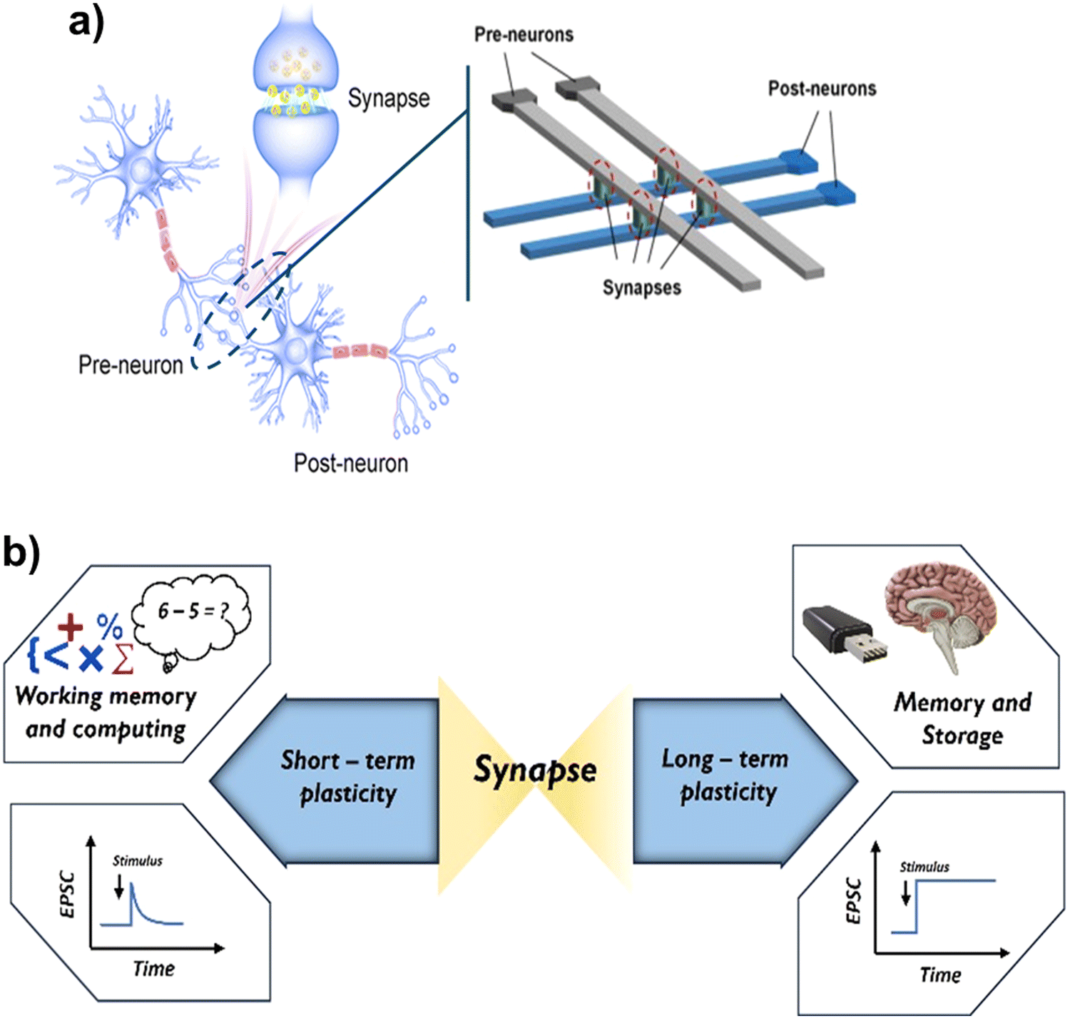 | ||
| Fig. 1 (a) Schematic of synaptic interface consisting of two layers of neurons and synapses. The synaptic function is emulated by memristors. The top electrodes of the devices connect to the pre-neurons, while the bottom electrodes to the post-neurons. Reproduced from ref. 8 with permission from Elsevier, copyright 2015. Reproduced from ref. 9 with permission from American Chemical Society, copyright 2021. (b) Schematic of short and long-term synaptic plasticity. STP relates to the working memory and computing, while LTP is attributed to long-term memory and storage. | ||
Various metal oxides have been explored as the active layer of a memristor with a range of internal resistive states, which can be modulated in a quasi-stable manner.3 Various binary oxides such as ZnO, CuO, TiO2, HfO2, ZrO2, NiO, VO2, MnO, Nb2O5, Ta2O5, WO2,12,13 transparent conducting oxides like ITO, and SnO2 are well known materials for anionic memristor devices. Perovskite systems, for instance, SrTiO3, BiFeO3, and SrZrO3, have also demonstrated the mechanism of valence change memory (VCM).12 Materials like GeOx, SiO2, and Ta2O5 layers can also be sandwiched between an electrochemically active (AE) electrode (such as Cu, Ag) and a counter electrode (such as Pt, W) to make cationic devices involving electrochemical metallization-mediated filament formation throughout the insulator. Furthermore, phase-change alloys have also been studied since their discovery.14,15 Temperature-triggered structural transitions in SrCoOx and VO216,17 have drawn the attention of neuromorphic electronics in recent years due to the correlated electron transport.
Being a Mott insulator, vanadium dioxide (VO2) can find potential application as an artificial neuron in achieving desired plasticity due to its negative differential resistance coupled with thermal hysteresis.16 The unique electric field-triggered phase transition behaviour, such as the high-resistance change rate, ultrafast response, and low-power consumption in VO2, provides a nonlinear dynamical response to input signals, as recommended to design neuromorphic circuit elements. Previously, VO2-based thin films and nanostructures were reviewed as thermochromic smart windows17–20 in correlation to the phase transition. Various reviews have emphasized its perspectives on tuning metal to insulator transitions (MIT)21 connecting to electronic21 and neuromorphic applications.22 The present review focuses on the recent advancements in VO2 memristor devices and the design of these devices into neuromorphic circuitry towards emulating the synaptic function, which facilitates a variety of applications such as in sensing, oscillators for spike coding, and neurorobotics.23 An outlook is provided on recent progress in different types of VO2 memristors with neuromorphic electronic circuitry, which can be a pathway towards hardware development of brain-like computing systems that can overcome the von-Neumann bottleneck.
2. Vanadium dioxide (VO2)
Vanadium (IV) oxide (VO2) is a unique correlated metal–oxide system exhibiting temperature-dependent reversible phase transitions. These Mott insulators with hysteretic metal-to-insulator transitions (MIT) are attractive in memristive circuitry where significant resistance changes can be accomplished.24,25 Vanadium can exist in oxidation states ranging from +3 to +5, giving rise to different oxides. Among 13 types of vanadium oxides, VO2 has proved to be an excellent candidate in photonic and electronic applications since Morin et al. at Bell laboratories observed its MIT in 1959.26 Interestingly, unlike other materials, Mott transition in VO2 is coupled with a reversible change from a monoclinic (M1) to a tetragonal-rutile type structure. This first-order phase transition was witnessed via in situ TEM at different temperatures, as depicted in Fig. 2(a).27In situ Fresnel microscopy has witnessed the development of abrupt tensile stress accompanied by MIT (Fig. 2(b)).27 VO2 can exist in various allotropic forms, such as M1, M2, M3, A, B, C, D, and T.19,28–30 In all the phases, each V atom is surrounded by six oxygen atoms, forming a distorted octahedron in which V atoms make an interpenetrating set of parallel chains. | ||
Fig. 2 (a) In situ TEM electron pattern and lattice images of monoclinic [![[1 with combining macron]](https://www.rsc.org/images/entities/char_0031_0304.gif) 12] and tetragonal [10] phases at 21 °C and 115 °C, respectively. The corresponding FFT patterns are shown as insets. (b) Electrical resistance and in situ wafer curvature stress measured across the phase transition during heating–cooling cycles in VO2. Reproduced from ref. 27 with permission from Royal Society of Chemistry, copyright 2013. (c) Change in the crystal structure and crystal field splitting across the phase transition in VO2. (d) Simulated band structure of VO2 in the rutile (metallic) phase and the monoclinic M1 phase. The band gap is about 0.68 eV. Reproduced from ref. 31 with permission from American Institute of Physics, copyright 2016. 12] and tetragonal [10] phases at 21 °C and 115 °C, respectively. The corresponding FFT patterns are shown as insets. (b) Electrical resistance and in situ wafer curvature stress measured across the phase transition during heating–cooling cycles in VO2. Reproduced from ref. 27 with permission from Royal Society of Chemistry, copyright 2013. (c) Change in the crystal structure and crystal field splitting across the phase transition in VO2. (d) Simulated band structure of VO2 in the rutile (metallic) phase and the monoclinic M1 phase. The band gap is about 0.68 eV. Reproduced from ref. 31 with permission from American Institute of Physics, copyright 2016. | ||
Monoclinic (M1 phase, P21/c) VO2 comprises V4+ ions paired along the c-axis, constituting a V–V chain with alternate long (3.12 Å) and short (2.96 Å) distances.19,32 The MIT in VO2 is mediated by the modification of the band structure near the Fermi level (EF).19 In the metallic state (tetragonal phase, P42/mnm), the mixture of dll orbitals that are directed along the rutile c-axis and antibonding π* orbitals are responsible for the density of states near the Fermi level. Across MIT, the dimerization of V ions results in splitting the d-band level into filled bonding and vacant antibonding levels. Simultaneously, π* orbitals transit to a higher energy state, leaving a gap between this band and the lowest occupied d‖ levels.19,33 The splitting of the 3d states of V4+ results in a bandgap of 0.7 eV between empty eπg and filled a1g bands.34 The structural transition accompanied by crystal field splitting is shown in Fig. 2(c). This can also be understood in terms of a charge density wave (CDW) formed along the rutile c-axis with a wave vector 2CR, causing the doubling of the unit cell along this direction. Therefore, both charge ordering, as well as dynamical correlations, contribute to MIT.35 Structure-driven Peierls transition (electron–lattice interaction) and Mott transition (electron–electron interaction) based on electron correlation also model the experimental results relating to MIT in VO2.36Fig. 2(d) shows the multiband system in which the M1 structure has a band gap of ∼0.7 eV, reflecting the breaking of structural symmetry.31
VO2 also exists in two other insulating phases: monoclinic M2 and triclinic T structures, which occur under uniaxial pressure or in doped samples.37 The structure still constitutes the dimerization of metal ions in the M2 phase, while dimerization is lost in other chains due to quasi-one-dimensional antiferromagnetic ordering. The T phase is intermediate to M1 and M2.37 VO2 undergoes first-order MIT at ∼341 K, leading to a sizable change in electronic and optical properties. Since the phase transition occurs at near room temperature accompanied by vast changes in electrical resistivity, VO2 (M1 and R) has spurred diverse applications in memory devices, frequency-agile metamaterials, smart windows, sensors, field effect transistors, and electrical switches.21,38 Meanwhile, VO2, with the B phase having an open framework, is a promising energy material that is used as electrodes in Li-ion batteries.39
2.1. Thin film deposition of VO2 polymorphs and memristor fabrication
As VO2 exists in different allotropic forms, as mentioned above, synthesis methods and conditions play a vital role in stabilizing thin films due to their complex structure. A major reason for the complexity of depositing these films lies in their narrow growth window, which uses various deposition techniques. Besides, these polymorphs are closely interrelated in a thermodynamical framework. For instance, VO2 with A and B phases are metastable in the bulk form, whereas they undergo a permanent phase change into the R phase upon heating.40 Epitaxial stabilization of crystalline solids employing a low energy interface is a practical approach in crystallizing single-phase material systems. Since both kinetic and thermodynamical factors influence the stability of these material systems, highly non-equilibrium film growth conditions are necessary, which are offered by various physical and chemical methodologies.Since vanadium and oxygen stoichiometry significantly impact the phase evolution and transition, a key to synthesizing VO2 is the precise control of stoichiometry, which avoids the formation of oxygen vacancies and other phases. Different VO2 epitaxial phases have been stabilized in various substrates such as silicon, quartz, and binary metal oxide single crystal substrates like Al2O3 and TiO2.41,42 VO2 epitaxy has also been achieved in perovskite substrates such as SrTiO3, TbScO3, (LaAlO3)0.3(SrAl0.5Ta0.5O3)0.7 (LSAT), LaAlO3 (LAO), and YaAlO3 (YAO) with (001), (011) and (111) orientation.39 In the last few decades, various methods have been developed for depositing epitaxial and nanocrystalline VO2, which affect its structure and morphology concerning its functional properties. The deposition techniques can be divided into two major parts: (i) vapor or gas phase deposition method, which primarily includes the physical and chemical transport of vapor onto a desired substrate, and (ii) solution processing in which wet chemistry is employed for desired phase formation and microstructure.
Pulsed laser deposition (PLD) is a common methodology for fabricating various metal oxides (Fig. 3(a)), including VO2.43 PLD is widely used in depositing VO2 polymorphs since Borek et al.42 successfully deposited highly oriented monoclinic (200) VO2 on r-cut sapphire substrates using vanadium metal as an ablation target. Since then, several reports are available in which vanadium metal,44,45 V2O5,41,46 V2O3,47 and VO248 were used as a source of ablation for the thin film deposition.18,49 Molecular beam epitaxy (MBE) is another PVD technique used for fabricating epitaxial layers with high reproducibility in terms of thickness and composition control at atomic levels (Fig. 3(b)). Challenges in the m-VO2 deposition via the MBE technique depend mainly on controlling the V and O beam fluxes for the stoichiometric deposition of the VO2.50,51 Indeed, maintaining the evaporation rate of V is difficult because of its low saturation vapor pressure and high melting point. Moreover, due to the multivalent states of vanadium ions and the high sensitivity to oxygen pressure, the vanadium–oxide may show different ionic states.52 Several groups have been successful in stabilizing different polymorphs of VO242,53,54 on various substrates in highly strained forms using MBE. VO2 has also been deposited using electron beam evaporation, wherein the evaporation of the vanadium target by electron beam in a pure oxygen environment is done.55 Formation of VO2via post-annealing of an electron beam evaporated vanadium film has also been observed.56 Reactive sputtering is another widely used method in fabricating VO2 thin films (schematic is shown in Fig. 3(c)).57,58 Advanced sputter deposition systems include reactive, magnetron, diode, triode, and ion beam sputtering. A variety of magnetron sputtering methods have been used in depositing VO2.59–62 High-density VO2 was deposited using ion-assisted dual ac magnetron sputtering in which films exhibited highly efficient thermochromism with high electrical and optical contrast.63–65 Recently, high-quality VO2 has been grown via a direct method of vapor transfer using V2O5 powder precursor in an inert atmosphere. Referring to schematic Fig. 3(d),66 nucleation of crystalline VO2 was carried out from molten V2O5 droplets without using oxygen-reactive gas, unlike other PVD methods.
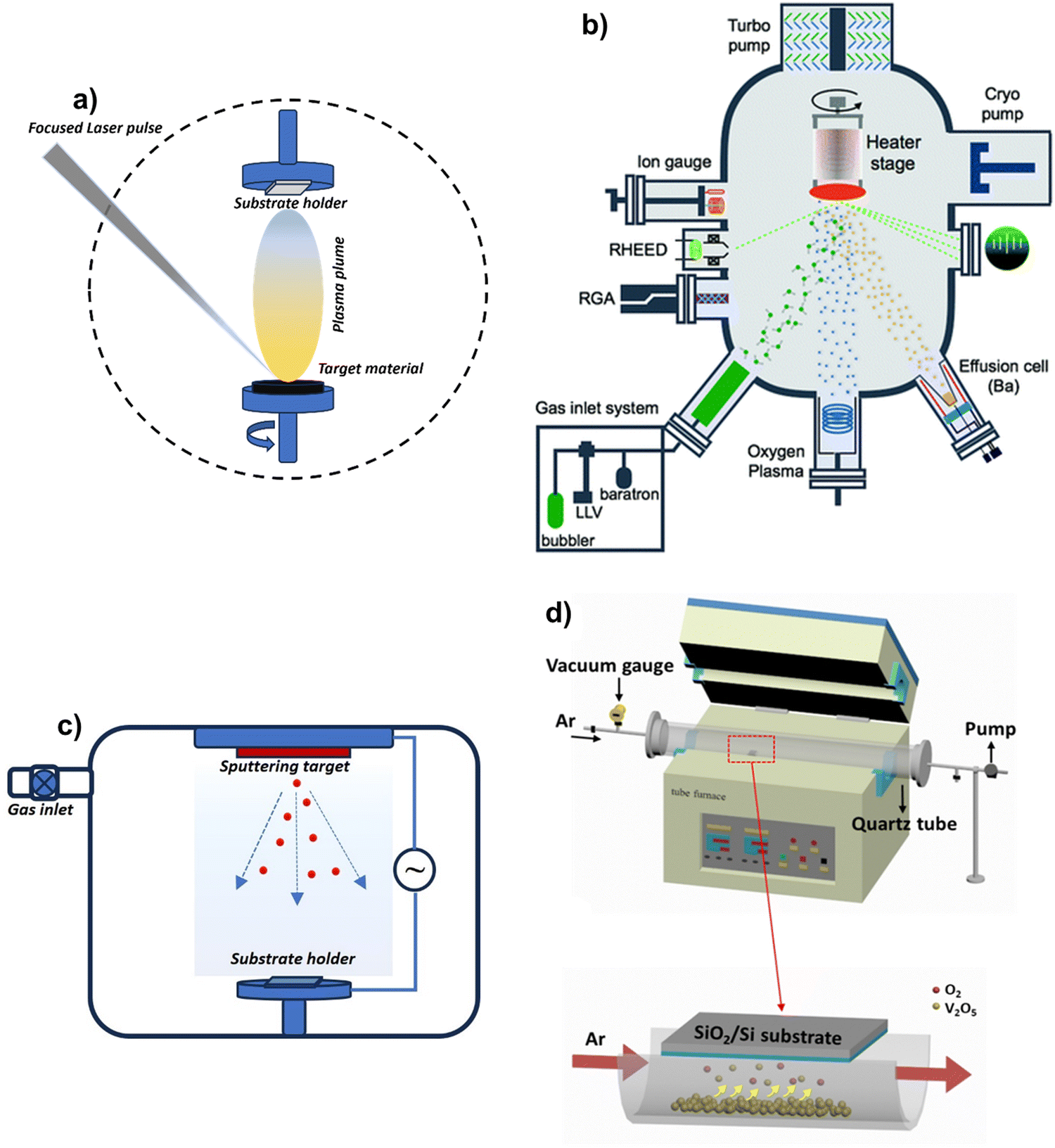 | ||
| Fig. 3 Schematic of the PVD systems, (a) reactive PLD, and (b) MBE. Reproduced from ref. 57 with permission from Royal Society of Chemistry, copyright 2017; (c) magnetron sputtering and (d) direct vapor transport method for depositing VO2 polymorphs. Reproduced with ref. 66 with permission from Nature, copyright 2021. | ||
Gas phase synthesis of VO2 includes chemical vapor deposition (CVD) techniques, which is possible with precise control of chemical stoichiometry. Organic precursors of vanadium(III), (IV), or (V) are used to deposit VO2 in oxidizing, reducing, and neutral environments.67,68 Aerosol-assisted CVD (AACVD) and atmospheric pressure CVD are widely used CVD methods in depositing VO2 thin films. Quite a lot of precursors, such as VOCl3,69 VO(iOPr)3,70 and VCl4 with ethyl acetate71,72 have been used to deposit VO2 on different substrates. Among various methods, atomic layer deposition (ALD) is a robust technique in depositing ultrathin VO2 films with mass production capabilities. Pure VO2 has been deposited with V(NEtMe)4 (tetrakis[ethylmethylamino]vanadium or TEMAV) as well as vanadium tris(N,N0-diisopropylacetamidinate) (V(amd)3) precursors using either water or ozone.73–75
Tuning the critical thickness to control the out-of-plane growth axis of VO2 across (020) and (200) on c-cut sapphire can be easily achieved using PVD techniques.76 Below the critical thickness, the formation of misfit dislocations can be arrested via strain trapping. This can easily be achieved via high-temperature processes assisted by PLD.77 Film thickness is also one of the factors that contribute to the modulation in V–V dimerization lengths, leading to the modified energy band gap and hence the Tc.78 Furthermore, MIT in textured VO2 films on amorphous and crystalline substrates can also be tuned by controlling the microstructures. The grain sizes of the VO2 films were tuned and compared with different PVD methods – PLD, and sputtering by Niang et al.79 Similar Tc, switching width and ratios are scaled as per the similar grain sizes.77 In nanocrystalline VO2, grain boundary fraction determines how MIT is scaled with film thickness. Decreased grain size leads to a fall in thickness accompanying the reduction in the resistivity ratios.80 According to the previous results, sputtered VO2 films were found to have the highest density whereas the ones deposited by e-beam evaporation had the lowest. In comparison with PLD and RF sputtering, VO2 films deposited by MBE were found to have minimal defects, on the other hand, PLD, sputtering and e-beam evaporation techniques were found to grow VO2 with moderate columnar and point defects. In general, MBE yields the largest grain sizes (100–500 nm) of VO2 films whereas sputtered films showed the lowest grain sizes (20–50 nm).81 Overall, the PVD process is more appropriate for fundamental research due to its precise control and compatibility with a wide range of substrates, especially for the fabrication of ultrathin film-based devices.
The M–I–M device structure employing VO2 as an active layer can be fabricated via stack-wise design and lateral electrode patterning. In general, metal oxide-based memristors are designed with electrodes with lower work functions to create a Schottky barrier across the interface. Top metal electrodes are generally deposited by sputtering and thermal/e-beam evaporation methods, and they are patterned using shadow masks or lithographic techniques. VO2-based memristors employ various metals such as platinum (Pt), gold (Au), silver (Ag), tungsten (W), nickel (Ni), and aluminium (Al)82–85 as well as a combination of Ti/Au, Au/Pt etc.86,87 as top electrodes (TE). The aforementioned metals were also used as bottom electrodes (BE) in stacked devices. Previous reports also suggest that conducting oxides such as Al:ZnO (AZO) and La0.7Sr0.3MnO3 (LSMO) can be effective bottom electrodes forming a heterojunction across the interface in which electron injection to the conduction band of VO2 is feasible due to the potential energy difference.88,89 Stacked devices are designed as simple as well as with hole-structured crossbar arrays. Crossbar arrays consisting of two resistive switching modes with one selector and one resistor (1S1R) cell are effective in avoiding issues due to sneak-path currents.84,89 In these devices, the area of the top electrode defines the size of each device. Generally, the top electrode thickness varies from 50–100 nm with width ranging from 2–500 microns. Formation and annihilation of conductive paths in VO2 devices also correspond to the non-linearity of the electric field applied to the nanoscale devices. Hence, devices with larger electrode areas tend to have unstable switching behaviours with narrow hysteresis as compared to the smaller ones.90 Metal electrodes are lithographically patterned over VO2 to form a bridge-type device in which the M–I–M structure is formed laterally. In this case, the electrodes are separated by a certain distance varying between hundreds of nanometres to a few microns.
2.2. Tailoring metal–insulator transition in VO2
VO2 stands out due to its unique MIT at near room temperatures, making it a promising candidate for neuromorphic electronics. MIT is accompanied with 3–4 orders of discontinuous switching in electrical conductivity along with thermal conductivity and transmittance switching. Transition between a low symmetry (M1) to a high symmetry (R) phase cause high (on/off) and low (off/on) resistance states of the materials induced by change in temperature.91 Tailoring the transition temperature (Tc), hysteresis size, and switching ratio serve as important parameters for in-memory computing applications, enabling the design of temperature-dependent spike-based circuitry. Various strategies have been adopted to modulate the MIT properties, including strain engineering, stoichiometric tuning, elemental doping, and nanocomposites, which is summarized in Fig. 4.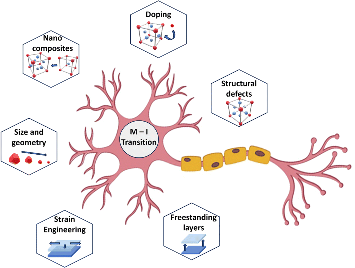 | ||
| Fig. 4 Strategies for tailoring MIT in VO2. This includes strain engineering, geometry engineering, introducing structural defects via stoichiometry, doping, composites, and the synthesis of free-standing VO2 layers via lift-off techniques. | ||
Along with temperature and chemical composition, strain is also critical in engineering the physical properties, especially in thin films. Nanoscale systems preserve increased elastic strain limits, leading to potential application prospects in the field. Chemical epitaxial strain is one of the fundamental factors that can be controlled by strain engineering, facilitated through the proper selection of substrate-film combination. The efficacy of strain engineering in epitaxial thin films mainly relies on the chemical and structural similarity of the substrate and the film.92,93 In the case of VO2, ultrafast spectroscopic studies have revealed that the transition temperature is connected to the strained state of dimerized V–V bonding along the c-axis.94–96 Previous reports have indicated the shifting of MIT towards room temperature due to the compressive strain along the c-axis; on the other hand, tensile strain shifts MIT towards higher temperatures.96 TiO2 is one of the popular substrates used in VO2 epitaxy since it is isostructural to the high-temperature phase (R) of VO2 with minor lattice mismatch (0.86% and 3.8% for the (001) and (110) orientation) enough to achieve epitaxial strain.97 In-plane anisotropic strain in the films can also be modulated by varying the thicknesses of the film; for instance, (110) VO2 films grown on TiO2 are found to show lower Tc with thickness due to strain relaxation.98 The interplay of lattice–electronic correlation is limited as the VO2 film is clamped to the substrate, and the MIT-based properties can be more pronounced if it is free from the substrate-induced strain. This idea has led to the development of free-standing VO2 membranes in which MIT has shifted towards room temperature, interestingly with a wider hysteresis.99 Recently, spurred by the technological interest in flexible electronics, research efforts have been made in fabricating freestanding VO2 by wet etching,99,100 ion milling,101 and mechanical exfoliation.102 In this case, a practical method is using a water-soluble sacrificial layer underneath the functional VO2, preferentially etching it from sideways using DI water. Freestanding membranes demonstrated wider hysteresis with reduced transition temperature, indicating the possible integration of the films into flexible electronic devices.99
Alternatively, intrinsic defects in VO2 play a key role in electronic transport, contributing to MIT. Oxygen vacancy (VO) defect doping in VO2 helps stabilize the rutile phase at room temperature.103,104 Movement of the Fermi level towards the conduction band has been observed with increasing VO, resulting in a narrowed energy band gap.105 Oxygen vacancies created up to an optimum non-stoichiometry contribute more carriers to the charge transport, and hence, the metallic character can be realized at lower temperatures.106 Formation of oxygen vacancies in VO2 having cations with single oxidation state can be written in terms of a defect equation 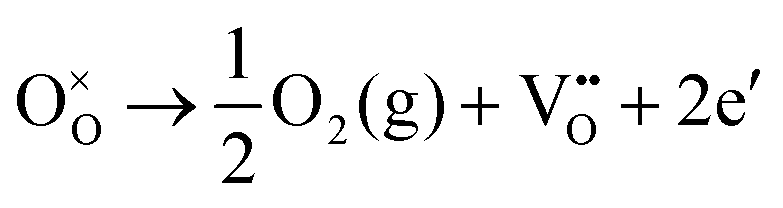 . When a metal cation is introduced with a different ionic state, the reaction will be of the type
  . In this case, the oxygen vacancy has to form to preserve the charge neutrality by either reducing the cation in the host material or donating electrons to the conduction band.107 Hence, oxygen vacancies induced by electron doping are one of the proven strategies for suppressing MIT temperature.108 Being a binary metal oxide, the single cationic site of VO2 is accessible to the metal dopants with higher and lower ionic states than the V4+ state. The electrical conductivity of VO2 can be increased by substituting the vanadium sublattice with metal ions with higher ionic state, for instance, doping elements such as W6+,109–111 Nb5+ (ref. 111 and 112) and Mo6+ (ref. 113) with ionic radii close to V4+ (58 pm)107 is termed electron doping, which adds extra electrons as a carrier to the system and helps break the dimerized V–V bonding states. Elemental doping with lower ionic states than V4+ is referred to as hole doping, which significantly reduces the energy band gap, leading to the stabilization of the R-phase beyond a critical hole density of 6.48 × 1021 cm−3. This is due to the strong dx2−y2–dz2 interaction in the vicinity of the Fermi level.114 Weakening of the dimerization could dominate the effect of electron correlation in the case of heavy hole dopants such as Cr3+,115,116 and Al3+,117 preferably shifting the Tc towards room temperature. Dopants introduce deep and shallow energy levels that reconstruct the electronic band structure. However, the increase in doping levels leads to increased degradation of the physical properties, which is driven by the phase transition. Lee et al.25 fabricated bilayers consisting of VO2 and VO2−δ with different transition temperatures. An attempt was made to achieve an isostructural metallic transition in insulating VO2 (M1) without any changes in crystallinity (see Fig. 5(a)). High and low-angle annular dark field (HAADF and LAADF) images in Fig. 5(b) depict the interface with cation and anion profiles. The difference in the contrast between HAADF and LAADF images differentiates the oxygen vacancy level across the nominal VO2/VO2−δ interface. The introduction of a small amount of oxygen vacancies creates a chemically sharp interface of heterostructures, which can be engineered by manipulating the phase transition characteristics.
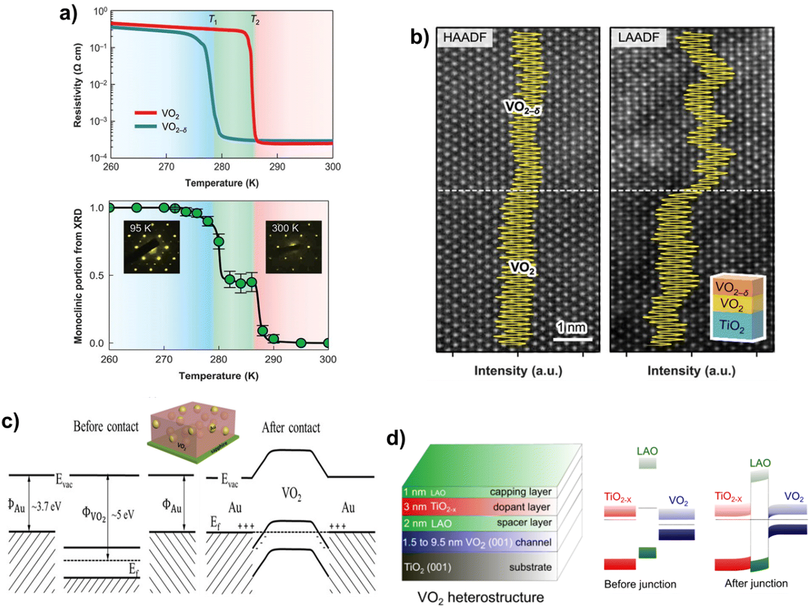 | ||
| Fig. 5 (a) Metal to insulator transition VO2/VO2−δ isostructural layers using temperature-dependent resistivity and X-ray diffraction measurements with the inset showing the electron diffraction patterns at 95 K and 300 K. (b) HAADF and LAADF images of VO2/VO2−δ bilayers. Reproduced from ref. 25 with permission from Science, copyright 2018. (c) Schematic and energy band structure in the Au:VO2 nanocomposite before and after embedding the Au nanoparticles. Reproduced from ref. 118 with permission from Wiley, copyright 2019. (d) Schematic of the VO2/LAO/TiO2−x heterostructure and energy band diagram before and after the junction formation. Electron accumulation is expected based on the known band offsets. EC, EV, and EF indicate the conduction band edge, valence band edge, and Fermi level, respectively. Reproduced from ref. 119 with permission from Nature, copyright 2023. | ||
Recently, the incorporation of a metallic phase in metal oxides as a metal–ceramic nanocomposite has emerged as a novel approach to tuning the Mott transition. In particular in Mott VO2, the introduction of a nanoscale metallic phase such as Pt or Au causes band bending across the metal:VO2 heterointerfaces, shifting the phase transition temperature.118,120Fig. 5(c) shows a schematic of metal embedded in the VO2 matrix, and Fig. 5(d) depicts the band structure and bending of Au:VO2. The Fermi levels are equalized, and the conduction band of VO2 bends upward, leaving an electron-rich area across the heterointerfaces. Thus, the introduced extra energy in the localized electrons in V–V pairs reduces the coulomb energy barrier, eventually lowering the phase transition temperature. Charge transfer assisted bandwidth controlled MIT in the Au–VO2 nanocomposite thin films were spectroscopically studied, in which a linear relationship was perceived between electron bandwidth and Tc.121 Recently, magnetic Ni inclusion in the VO2 major matrix has been found to tune the MIT across a broad range of temperatures, paving the way for advanced electronic and spintronic device applications.122 The concept of modulation doping was introduced in a recent study119 in which TiO2−x (dopant) and LaAlO3 (spacer) layers were deposited over a VO2 channel layer and capped using LaAlO3 (see Fig. 5(d)). The idea was to achieve higher dopant concentrations via a mismatch in chemical potential between the dopant layer and the undoped channel layer. A spacer layer is used to limit the dopant interdiffusion across dopant and channel layers during the quantum mechanical tunnelling of the charge carriers. The band alignment of these heterostructures is shown in Fig. 5, illustrating the Fermi level alignment leading to an electron accumulation layer across the LAO/VO2 interface. The shifting of the Tc towards lower temperatures is evident with increased carrier density, signifying the closeness of the modulation doping to the elemental doping in achieving high carrier density.
Modulating the Tc and the hysteresis width in a typical correlated electron VO2 system is essential in enabling the design of a memristor whose internal resistive states can be tuned at different temperatures. Strain engineering is practical in epitaxial or nanocomposite films via misfit strain, which mainly depends on selecting an isostructural interface between the film and the substrate.
2.3. VO2-based memristor devices
In VO2 based memristors, the filaments are found to be composed of strongly correlated phases of VO2 along with redox reaction. As the commanded voltage input in the VO2 device is raised, the temperature of the device will increase owing to the Joule effect. This leads to the formation of metallic crystallites with lower resistance until it reaches a point of percolation creating a conductive pathway of metallic VO2 in the device. Hence, when the MIT is driven electrically, the variation in resistance is filamentary as reported previously.82,125 This phenomenon can be employed in designing a static spiking sensor in which the variation in resistivity changes the firing frequency of an RC circuit. In addition, this oxygen migration can lead to other oxygen-deficient vanadate phases within the VO2 film facilitating filament formation. Recent studies have also witnessed that the filament formed across the VO2 device is also composed of metallic V5O9. The formed filament shortens the electrodes, allowing a large current across the device. The V5O9 is another correlated electron phase of vanadium-based oxides with lower ionic states than V4+ as confirmed by the redshift of the oxygen K edge in the electron energy loss spectrum (EELS).87 Since VO2 exhibits thermal-induced abrupt change in resistivity along with negative differential resistance (NDR), spiking neural networks can easily be modulated by temperature as well as electrical means.126
The device architecture in which the metal electrodes are patterned over VO2 consisting of a nanochannel of active layers has witnessed stable resistive switching. Filament formation was also experimentally imaged in these devices with a gap distance of a few hundred nanometres, showing a volatile resistive switching.127 Phase transition can be invoked in these devices with patterned electrodes separated by a nanoscale VO2 channel through current-induced Joule heating and temperature sweeps. 2D XRD maps in Fig. 6(a) depict the volatile switching in the device in which stepwise fractional gain of the rutile phase in current off-to-on states is visualized. The device switches via the formation of a continuous filament composed of a rutile phase (see Fig. 6(b)). The results suggest that the temporary crystal lattice disorders created via the application of electric current are effective in stabilizing the reversible phases, which enables the reversible modification of the local switching response between persistent and volatile modalities. This helps in controlling the switching behavior via manipulating local defect concentrations induced by the magnitude and duration of the electric current.
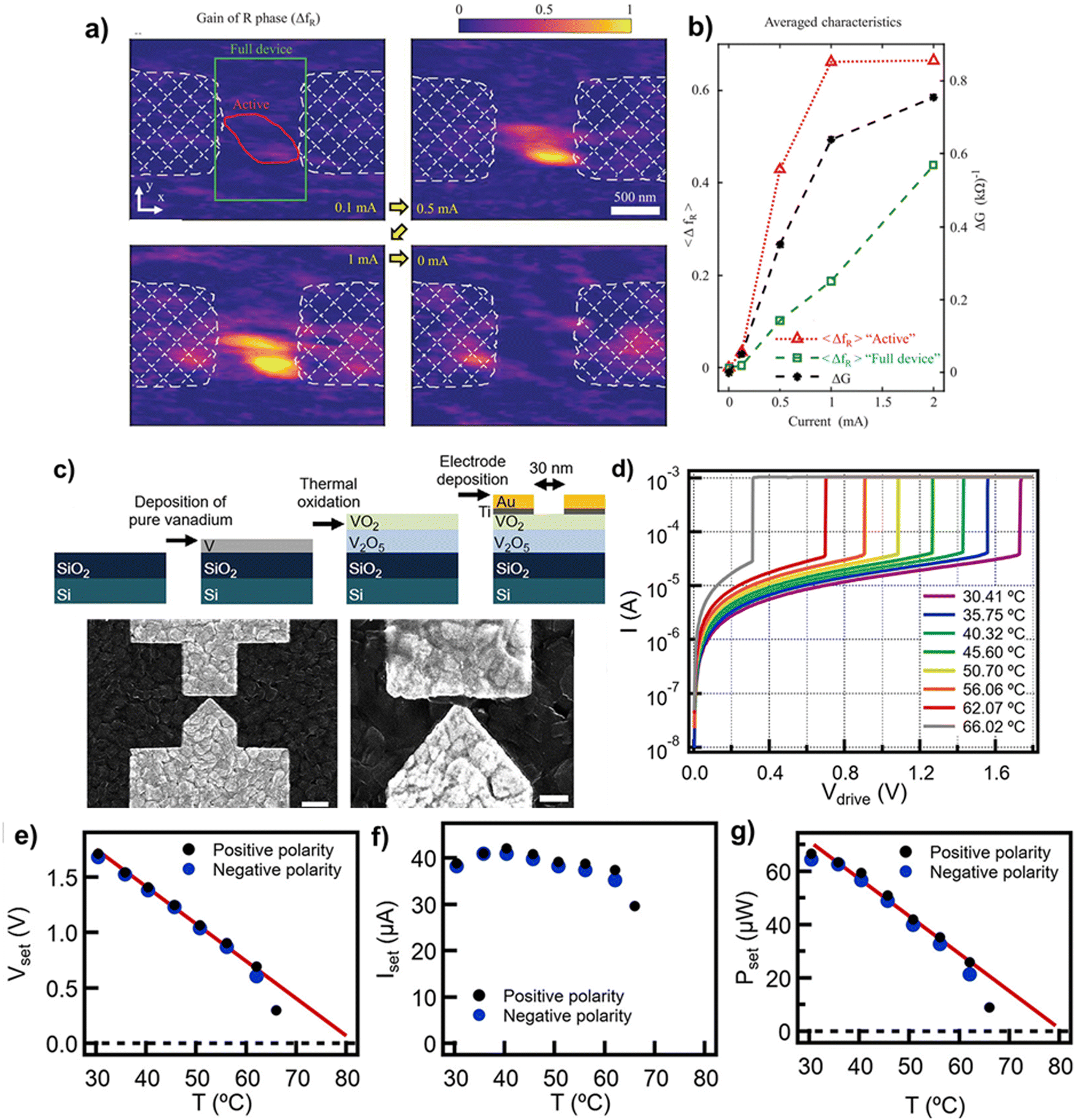 | ||
| Fig. 6 (a) 2D map of volatile resistive switching in VO2 with the gain of R phase fraction measured at different current values. Green and red contours outline the regions of “Full device” and “Active” used for averaging; (b) average characteristics of current dependence of the conductance (black curve) and the gains of the R phase averaged over the regions of “Full device” and “Active” (green and red curves). Reproduced from ref. 127 with permission from Wiley, copyright 2020. (c) Schematic, fabrication steps of the nanosized VO2 phase change memory devices. The cross-section is taken parallel to the nanogap axis. SEM micrograph of the device before and after performing the electrical measurements. Temperature dependency of (d) set voltage (Vset), (e) set current (Iset) and (f) set power (Pset) of the aforementioned device. (g) Current–voltage characteristics on logarithmic current scale recorded at different base temperatures for the aforementioned device. Reproduced from ref. 128 with permission from American Chemical Society, copyright 2023. | ||
NDR, oscillations, and instabilities in VO2/SiN lateral devices were observed via in situ thermoreflectance mapping with a steady-state electrical bias.129 These studies have witnessed the monotonic increase in channel temperature caused by self-Joule heating, which is the primary factor leading to NDR, instability, and oscillations. The coupled thermal and electrical nonlinearities can also create instability in NDR and local oscillations in VO2. Previous studies have witnessed the electric current-induced breakdown of the device accompanied by the surface melting, coalescence, and ablation of VO2 picturized in terms of scanning X-ray nano diffraction and atomic force microscopy (AFM).130 A similar lateral device with Au/VO2/V2O5/SiO2/Si stack consisting of 30 nm active space (Fig. 6(c)), exhibited the switching ratios 104–105 at room temperature.128 Upward voltage sweeps between 34–66 °C witnessed a stable resistance switching with decreasing set voltage with the Tc being triggered by both thermal and electrical means. Set voltage (Vset) was observed to decrease with an increase in electrode spacing, underpinning the advantage of device geometry with respect to energy consumption. Referring to Fig. 6(d)–(g), a linear tendency could be seen in the decreasing Vset values as the temperature is increased, whereas set current (Iset) and set power (Pset) were found to be constant.128 Planar bridge structured devices have been fabricated with the Au/VO2/TiO2 configuration having bridge lengths ranging from 10–20 μm.131 Multi-state memory controlled via voltage or current was realized, and over eight separable states were achieved, corresponding to three bits per cell. Recently, Liu et al.132 fabricated a calibratable memristor consisting of an 8 × 8 VO2 array based on which a frequency convertor was also designed. The current-driven I–V curve read out using an oscilloscope suggests the self-oscillation phenomenon occurring due to the quasi-static NDR. To make use of this phenomenon without any external resistance into a calibratable oscillator, the memristor was connected parallel to a capacitor and a resistor (to convert current to a voltage output). Schmid et al.133 demonstrated that resistive switching in VO2 can be as fast as up to 15 picoseconds under electrical stimuli. They analysed current evolution with an applied voltage pulse lasting for 20 ps and it was observed that MIT was triggered with very little Joule heating, as low as a few femtojoules. After confirming the HRS in these Au/Ti/VO2 devices, a 20 ps pulse with varying amplitude was applied followed by a 1 ns long read pulse of 0.25 V. Moreover, a V-shaped electrode helped facilitate fast thermal relaxation and sub 100 ps MIT in VO2.
A recent in-operando TEM study on electroforming in Au/VO2/Ge vertical devices witnessed the formation of conductive filaments composed of V5O9 (see Fig. 7(a)). Interestingly, another pronounced MIT at 140 K corresponding to the correlated V5O9 phase was observed in the temperature-dependent electrical resistance of the device after electroforming.87 Bao et al. designed a tunable stochastic memristor with a VO2/TaOx bilayer structure.134 The device demonstrated threshold switching along with random resistive switching, which helped accomplish tunable stochastic oscillations for compressed sensing. Xue et al.82 found a solution to the sneaking path and misreading problems in high-density crossbar memristor arrays using a Pt/VO2/Pt sandwiched selector device (S) integrating it with a HfO2 memory cell (R) into 1S1R architecture, as shown in Fig. 7(b). Coincidently, both the memory cells were found to operate at the same operating range, and the 1S1R device exhibited stable switching over 107 cycles with an on–off ratio over 10 (see Fig. 7(b) and (c)). Interestingly, they realized the formation of a one-dimensional nanochannel composed of VO2 mediated via electrically induced ion migration in Pt/V2O5/Pt devices. Near-room temperature MIT was observed in VO2 induced by the electric field with a sharp response of 0.5 mV K−1 and low energy consumption of ∼8 pJ. Fig. 7(d) and (e) depict the circuit designed for controlling the transition speed and characteristics in which the switching speed of 17 ns was achieved.82 Flexible VO2 memristors were fabricated with the stack of nanolayers sputtered over a flexible PEN substrate with functional and electrode layers patterned via lift-off processes.135 The device exhibited endurance of over 104 sweep cycles with bending stability over 103, and was able to oscillate under the current source, as shown in Fig. 7(f). The device switched 108 times across low and high resistance states within 104 s, driving a current of 130 μA. VO2 has been successfully employed as an active layer in which NDR can be tuned with a combination of voltage and temperature. Large on/off ratios, high linearity, and I–V symmetry make VO2-based memristors ideal candidates for neuromorphic computing. Furthermore, the stable operations of these devices are ensured by the reliable endurance and retention characteristics of the devices. A summary of the VO2 memristor device structure and parameters is given in Table 1.
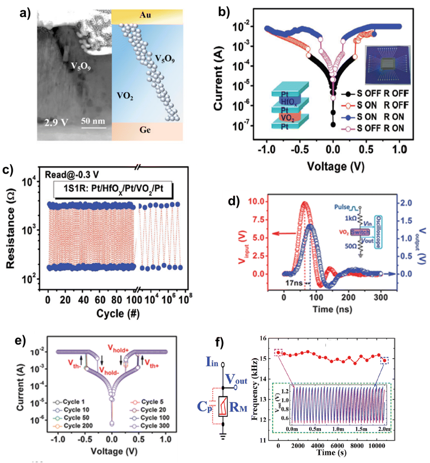 | ||
| Fig. 7 (a) TEM micrograph and the corresponding schematic of the conductive filament composed of V5O9 in Au/VO2/Ge devices. (b) I–V characteristics of the Pt/HfO2/Pt/VO2/Pt 1S1R structure with the inset showing the schematic of the heterostructure and digital image of a 20 × 20 crossbar array. (c) Endurance performance of the 1S1R structure with the writing/erasing pulse pair of – (±1 V, 20 ns) and read voltage of −0.3 V, respectively. (d) Circuit design and input/output signal evolution for switching speed measurement of VO2 MIT. (e) Threshold switching characteristics of the VO2 memristor for over 300 consecutive cycles. Reproduced from ref. 82 with permission from Wiley, copyright 2017. (f) Oscillation circuit of the flexible VO2 Mott memristor and corresponding variation in spiking frequency and measured time under oscillation conditions at room temperature with the driven current Iin = 130 μA. Reproduced from ref. 135 with permission from Wiley, copyright 2022. | ||
| Device structure | On/off ratio | Set voltage (V) | Endurance | Ref. |
|---|---|---|---|---|
| Ag/VO2(B)/SiOx on n++ Si and Ag/VO2(B) on n++ Si | 60 | 2–3 | Over 30 cycles | 136 |
| Pt/HfO2/Pt/VO2/Pt on SiO2/Si | >10 | ∼0.6 | 107 cycles | 82 |
| Pt/VO2 on Pt | ∼200 | 2.5 | Over 120 cycles | 137 |
| VO2 on TiO2 lateral Ti/Au contacts | 10 | 1.7 and above at increased bias | — | 131 |
| Au/VO2 on Ga doped Ge | ∼10 | ∼3 | — | 87 |
| Ti/Pt/VO2/Pt on PEN | >10 | ∼1.8 | Over 104 cycles | 84 |
| Pt/VO2/Ti/Pt on PEN | >10 | ∼0.65 | Over 104 cycles | 135 |
| TiN/VO2/TaOx/Pt on SiO2/Si | >10 | 1.124 | — | 134 |
| Au/Ti/VO2/Au/Ti lateral structure on V2O5/SiO2/Si | >10 | 1.71 | 105 cycles | 128 |
2.4. VO2 memristors in neural spiking
Realizing brain-like computing using VO2 memristors lies in emulating the synaptic function, which facilitates various applications in sensing, oscillators for spike coding, mechanoreceptors, and anthropomorphic neurorobotics. Since MIT is closer to the body temperatures of homoiotherms and due to the sensitivity at near ambient temperatures, VO2 can be an excellent temperature sensor. A VOx layer stacked between platinum layers was utilized in emulating synaptic functions.138 Sequential pulses applied on the devices were found to evoke gradual changes in current, thereby emulating LTP and LTD functions. The energy consumption for these devices was 270 μJ for an electrode area of 1 mm2. Exploiting the unique memristor characteristics, a flexible artificial spiking warm receptor was designed by Han et al.135 The device output spike frequency could change with the stimulus temperature, bearing similarity to the response characteristics of biological warm receptors. With the stimulus temperature raised from 20 to 40 °C, the frequency of the spikes increases from 16.8 to 60.2 kHz, beyond which it quickly decreases to zero at temperatures greater than 45 °C. The temperature-dependent variations in spike frequency and circuit design are shown in Fig. 8(a). In another study, VO2 memristor-based mechanoreceptors were designed with three receptors obtained by connecting a flexible VO2 memristor with three pressure sensors in series.84 The hole-structured crossbar of the Ti/Pt/VO2/Pt layers was fabricated on flexible PEN substrates. The device successfully mimicked the functions of sensing, coding, and fusing spatiotemporal pressure information into spike trains, providing a direction toward the futuristic development of anthropomorphic neurorobotics. Yuan et al.23 fabricated a calibratable artificial sensory neuron (CASN) involving an epitaxial VO2 planar memristor device coupled with a calibration resistor. A spike-based neuromorphic perception system with spiking curvature sensory neurons was employed to attain hand gesture recognition experimentally. With the curvature sensor affixed to the finger, the curvature sensory neuron's spiking frequency depends on the finger's bending. A considerable decrease in spike frequency with an increase in curvature is depicted in Fig. 8(b). They have also developed sensory circuits to emulate tactility, vision, and temperature, which operate based on the change of frequency induced by the stimulus to different extents. As shown in Fig. 8(c) and (d), the effect of pressure and illuminance is to increase the spike frequency. | ||
| Fig. 8 (a) Spike rate of the VO2 warm receptor in response to the stimulus temperatures, with the inset showing the warm receptors in the skin, transmitting rate-coded spikes. Spiking frequency variation with the stimulus temperatures and the inset is the circuit diagram of the artificial warm receptor and output spikes for different stimulus temperatures driven by a current source of 110 μA. Reproduced from ref. 135 with permission from Wiley, copyright 2022. (b) Schematic of artificial spiking tactile sensory neurons and output spikes at different curvatures. (c) Change in output frequency with pressure for VO2 tactile sensory neurons with the circuit schematic in the inset; (d) change in output frequency with illuminance for VO2 vision sensory neurons with the inset showing the circuit. Reproduced from ref. 23 with permission from Nature, copyright 2022. | ||
A traditional physiological signal processing system employs analog-to-digital converters (ADC), which convert the analog physiological signal into digital. Then, they are stored in memory units before being further processed in digital computing units. As the enormous amount of data flows across memory and computing units, power consumption and speed are considerably affected. Recently, a physiological signal processing system was designed based on VO2 memristors, which incorporates an asynchronous spike encoder and a long short-term memory spiking neural network (LSNN)-based decision system.139 Leaky integrate and fire (LIF) neurons can be realized by a circuit in which the VO2 memristor was parallelly connected to a capacitor in series with a load resistor RL. A 50 Ω resistor (R0) was used to convert the current into a voltage output (Fig. 9(a)). It was observed that higher series resistance and lower input voltage resulted in a lower charging current, thereby lowering the firing frequency of the neuron (Fig. 9(b) and (c). The same circuit was modified with an adaptive control circuit containing a feedback connection to form an adaptive leaky integrate and fire (ALIF) neuron. Each spike from the LIF part leads to the charging of capacitor C2 and an increase in voltage Vg, which turns on the transistor M3, resulting in an increased leakage current and, hence, the adaptation. The spike frequency is independent of Vg (transistor M3 is off), increasing monotonically as Vg increases. The adaptive response of Vg, Vm, and Vspike is depicted in Fig. 9(g). Thus, the designed neurons are observed to be superior to the existing CMOS in terms of speed, energy consumption, and area.
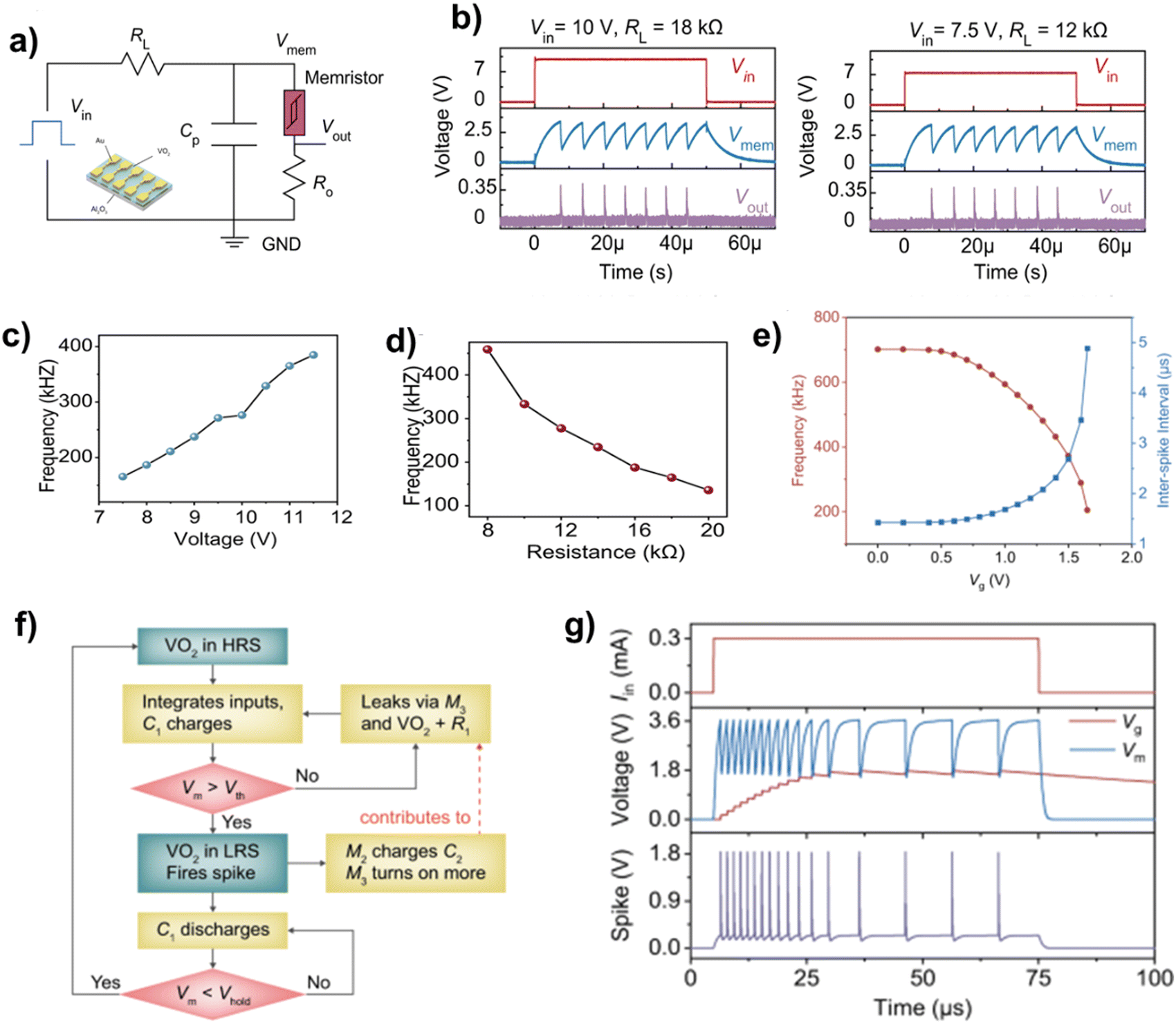 | ||
| Fig. 9 (a) Circuit design of artificial VO2 LIF neurons with device structure in the inset. (b) The artificial neuron response under different series resistance and applied voltage. (c) and (d) The effect of series resistance and applied voltage on spiking frequency. (e) Effect of Vg on the spiking frequency and its reciprocal, the inter-spike interval of the VO2 adaptive LIF neuron. (f) Flowchart of the operation of the ALIF neuron. (g) Adaptive response of Vg, Vm, and Vspike when the input current is 0.3 mA. Reproduced from ref. 139 with permission from Nature, copyright 2023. | ||
Artificial neurons constructed using Mott VO2-based memristors can be assembled hierarchically into dynamic network structures relying on the choice of conducting pathways linked with filaments and multilayer electrodes, as shown in Fig. 10(a). Such a dynamic network consisting of VO2 memristors via controlling the location of filament formation depending on the electric field-induced localized MIT was newly proposed by Feng et al.140 Planar VO2 MIM structures were patterned with a common terminal consisting of a round electrode that mimics a biological dendrite attached to a DC and microwave source through a bias tee. The rest of the electrodes, resembling presynaptic terminals, were ground. Defect-induced hot spots under the DC bias triggered the spontaneous formation of the filament location. Defect-induced hot spots were also created via laser-induced heating to rearrange conducting filament channels formed above the threshold DC bias to the different MIM locations (Fig. 10(b) and 10(c)). A square wave with an amplitude of 0.5 V and frequency of 25 MHz is applied to the common electrode through a bias tee as a signal source. Another bias tee is used to connect an oscilloscope with a 50 ohms internal resistance in series between channel C and the ground to monitor the transmitted AC signal. The amplitude of the transmitted signal as the filament is formed in each channel (as shown in Fig. 10(d) and (e)). When the filament is created in channel C, its amplitude is about 60 times greater than the other channels, as shown in Fig. 10(f).
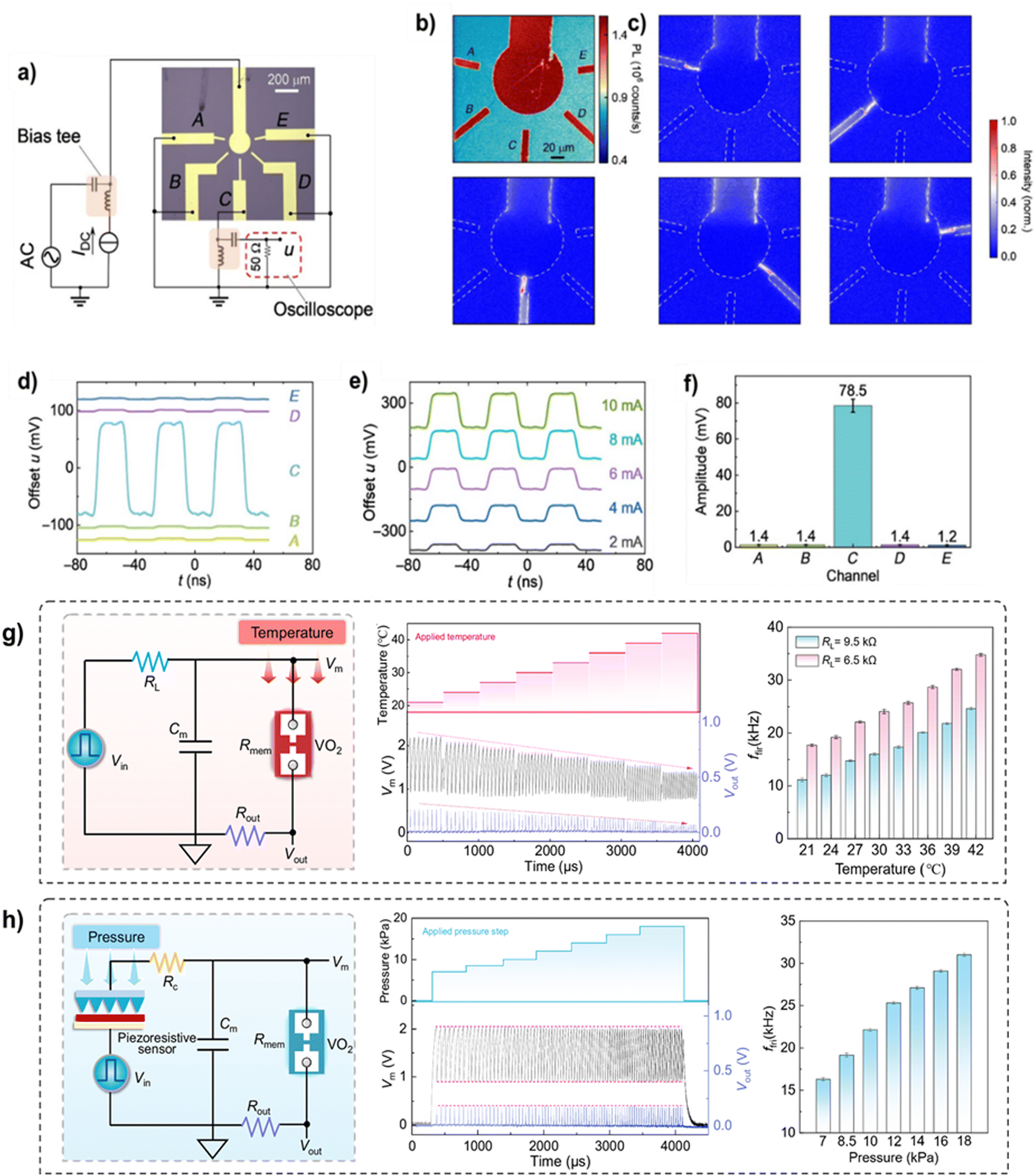 | ||
| Fig. 10 (a) Schematic of capturing the signals transmitted through the network structure consisting of artificial synapses based on VO2. (b) Confocal PL images of NV centers in the vicinity of a network structure with five artificial synapses constructed by a VO2 film. (c) The filament formation is switched with the help of DC bias and a laser spot. (d) Transmitted signal of channel C when a filament is formed by the focused laser and triggered by a 10-mA current. (e) The transmitted signal of channel C is controlled by DC current as the filament is formed in channel C. (f) The amplitude of the transmitted signal as the filament is formed in each channel. Reproduced from ref. 140 with permission from Science, copyright 2024. Artificial spiking neuron for (g) temperature and (h) pressure sensing applications, showing the variation of voltage and frequency under the stimuli. Reproduced from ref. 141 with permission from Nature, copyright 2024. | ||
Based on the NDR behaviour of VO2, Yang et al.142 proposed a dendrite-like functioning neuron termed an NDR neuron. XOR logic was easily performed through a single-layered neural network with NDR characteristics. The NDR neuron was found to occupy only 0.2 μm2 area with an average power consumption of 29.6 pJ per conversion in neural networks. Recently, a new class of spiking oscillators based on MIT of VO2 was developed to form a ‘thermal neuristor’.143 This dynamic system consists of two spiking oscillators coupled thermally based on VO2 insulator. When these coupled neuristors are biased at their respective subthreshold voltages, one neuristor excites the other resulting in 1![[thin space (1/6-em)]](https://www.rsc.org/images/entities/char_2009.gif) :1 synchronisation of both phase and frequency. The synchronisation of the frequencies was also varied to 2:1 and 3:1 modes with different suprathreshold voltages. Hence, the brain's dynamic behaviour can be mimicked with distantly positioned neuristors. One of the recent reports deals with the crossmodal spiking sensory neuron (CSSN) to aid haptic feedback for an in-sensor computing system and to process multimodal signals developed using a flexible VO2-based memristor.141 The CSSN mainly includes two components, a flexible pressure sensor and a temperature-sensitive memristor. The real-time responses of the sensory neuron circuit were recorded by applying different temperatures (21–42 °C) and pressure (0–18 kPa). The output firing frequency of the neurons was found to increase with temperature as well as pressure as shown in Fig. 10(g) and (h), which also depicts the circuit employed for the operation. They depicted the higher recognition accuracy (98.1%) of multimodal systems over single modal sensors. A similar structured VO2 coupled oscillator was also reported to execute dynamic sensory performance adopting near-sensor computing.144 This oscillatory circuit aims for a decision-making neural network and a low-level phase difference encoding in hardware. The outcome was high cycle-to-cycle uniformity with oscillation frequency up to 26 MHz with an energy-delay product (EDP) of 3.07 pJ and a delay time of 20 μs. Galloni et al.145 tried emulating temporal integration as well as associated memory of neurons by controlling the MIT in VO2. It is evident from the report that the slow decay of neuronal internal variables can be mimicked by the dynamical control of the kinetics of MIT. The behavioural timescale synaptic plasticity (BTSP) learning rule utilizing a slow analog state variable was also demonstrated. Li et al.146 demonstrated that the phase transition in VO2 can be regulated by UV photons, thereby confirming the fact that UV light perception can be realized with storage functions. A similar OES device with VO2/MoO3 was also demonstrated in recent times using near-infrared illumination to realize synaptic plasticity.147 An artificial spiking photoreceptor (ASP) was fabricated by Han et al.,148 consisting of a single VO2 Mott memristor to detect the light stimulus and imitates the human retina via converting the light intensity into encoded spikes. This can open up the way towards a next-generation optical communication system.
:1 synchronisation of both phase and frequency. The synchronisation of the frequencies was also varied to 2:1 and 3:1 modes with different suprathreshold voltages. Hence, the brain's dynamic behaviour can be mimicked with distantly positioned neuristors. One of the recent reports deals with the crossmodal spiking sensory neuron (CSSN) to aid haptic feedback for an in-sensor computing system and to process multimodal signals developed using a flexible VO2-based memristor.141 The CSSN mainly includes two components, a flexible pressure sensor and a temperature-sensitive memristor. The real-time responses of the sensory neuron circuit were recorded by applying different temperatures (21–42 °C) and pressure (0–18 kPa). The output firing frequency of the neurons was found to increase with temperature as well as pressure as shown in Fig. 10(g) and (h), which also depicts the circuit employed for the operation. They depicted the higher recognition accuracy (98.1%) of multimodal systems over single modal sensors. A similar structured VO2 coupled oscillator was also reported to execute dynamic sensory performance adopting near-sensor computing.144 This oscillatory circuit aims for a decision-making neural network and a low-level phase difference encoding in hardware. The outcome was high cycle-to-cycle uniformity with oscillation frequency up to 26 MHz with an energy-delay product (EDP) of 3.07 pJ and a delay time of 20 μs. Galloni et al.145 tried emulating temporal integration as well as associated memory of neurons by controlling the MIT in VO2. It is evident from the report that the slow decay of neuronal internal variables can be mimicked by the dynamical control of the kinetics of MIT. The behavioural timescale synaptic plasticity (BTSP) learning rule utilizing a slow analog state variable was also demonstrated. Li et al.146 demonstrated that the phase transition in VO2 can be regulated by UV photons, thereby confirming the fact that UV light perception can be realized with storage functions. A similar OES device with VO2/MoO3 was also demonstrated in recent times using near-infrared illumination to realize synaptic plasticity.147 An artificial spiking photoreceptor (ASP) was fabricated by Han et al.,148 consisting of a single VO2 Mott memristor to detect the light stimulus and imitates the human retina via converting the light intensity into encoded spikes. This can open up the way towards a next-generation optical communication system.
Recently, VO2-based nanocomposites have also been explored for memristor applications. A nanocomposite-based lateral device of VO2 with CNT demonstrated periodic spikes of sub-20 ns width driven by voltage or direct current without any assistance of an external capacitor.149 The device behaves as a relaxation oscillator with a capacitor connected in parallel, driven by a DC source. Here, the usage of CNTs as a nanoscale heater has increased the spike frequency considerably up to three orders of magnitude. A recent study of VO2/TiO2 nanotube composite films found that the composite structure enhances the switching and synaptic characteristics via reducing the resistance of the active layer, helping in promoting the formation of Ag conductive filaments.150 The Ag/VO2/TiO2 devices were found to improve the accuracy of image recognition. Hence a composite structure can help in locally confining the effective thermal structure, thereby engineering the dynamical properties.
Being a bipolar switching redox memristor, the VO2-based MIM structure is compatible with the existing CMOS process. However, temporal stochasticity is reflected in all these devices with cycle-to-cycle or device-to-device variations in resistive states. Randomness in conductive path formation and rupturing processes lead to these conditions, making them unfavourable for storage class memory applications.151 In VO2-based memristors, this stochasticity is desirable when used in neural networks mimicking the stochastic resonance or probabilistic spiking.152 In the case of sensory networks in which the power of the stimulus is encoded in spike rate, the detection limit may deteriorate due to the stochasticity. Abrupt phase transition of VO2 enables the aforementioned ultrafast switching devices, but relatively high MIT can lead to high energy loss and thermal-induced damages to the device assembly. Hence, the modified VO2-based systems with well-modulated MIT that retain the rapid response and high switching are needed for practical neuromorphic applications. A brief summary of spiking circuits with operation parameters is given in Table 2.
| Device structure | Application | Frequency range | Energy consumption | Ref. |
|---|---|---|---|---|
| Pt/VO2/Ti/Pt/Al2O3 on PEN | (1) Warm receptor | 60.2–16.8 KHz for 40–20 °C | — | 135 |
| (2) Oscillator | 16.8 kHz | |||
| Au/VO2/Au on c-Al2O3 | (1) LIF neuron | 100–400 kHz | 86.5 fJ per spike | 139 |
| (2) Adaptive LIF neuron | 100–700 kHz | 338 fJ per spike | ||
| Pd/VO2/CNT/Pd on TiO2 | Relaxation oscillator | ∼500 kHz | 1.3 pJ | 149 |
| Ti/Au/VO2/Ti/Au on Al2O3 (012) | Thermal neuristor | — | 5.56 nJ per 14 spikes | 143 |
| Au/VO2/Au on SiO2/Si | (1) Temperature sensing | ∼10–25 kHz (21–42 °C) | 3.9–50 nJ per spike | 141 |
| (2) Pressure sensing | ∼17–31 kHz (1–18 kPa) | |||
| Au/Ti/VO2/Au/Ti on c-Al2O3 | (1) Oscillator | 26 MHz | EDP – 3.07 pJ | 144 |
| (2) Touch and pressure sensor | ||||
| Pt/VO2/Pt on silicon nitride covered Si | Active memristor neuron | 5–50 kHz (instant. spike frequency) | >0.1 pJ per spike | 152 |
Collectively, these studies contribute to developing hardware neural network systems with brain-inspired algorithms and enable the application of neuromorphic computing. The studies in the past few years have accessed the suitability of VO2-based memristors in mimicking the functions of the human brain. These devices find practical applications in sensing temperature, illumination, curvature, etc. The direction of research in these systems has moved towards artificial intelligent systems via the design of efficient neurorobotic circuits.
3. Summary and outlook
VO2 stands out as a unique material beholding the intrinsically coupled electronic and phase transitions. Herein, the current trends in VO2 memristors for brain-inspired computing are summarised with a detailed discussion on the memristor behavior in correlation to the neural spiking applications. Tailoring the MIT serves as an initial step towards realizing desired memristor performance at desired temperature. Novel strategies such as synthesis of freestanding epitaxial VO2 are extremely helpful in modulating the MIT, towards the fabrication of flexible memristors. Versatile and practical integration of high-quality MIT can open the doors towards wearable neuromorphic devices.As high-performance VO2 thin films were reportedly fabricated at high temperatures, one of the challenging tasks is to reduce the synthesis temperature while maintaining the quality simultaneously. Despite the high stability and flexibility of the spiking devices, large scale integration without compromising the performance is needed. Moreover, handling the energy consumption of these devices with the increase in number of nodes is still an issue of concern. Currently, the scope for the advancement in this class of devices lies in designing better device architecture, and circuit design to overcome the aforementioned roadblocks. Furthermore, modulating the device performance requires optimization of the material properties as well as potentially realizing advanced neuron circuitry. Since, metal–VO2 epitaxial nanocomposites allow a broadband tuning in Tc, memristor architectures with composite thin films will provide access to tune the sensory behaviour, making it an active area of research. As per the recent trends, lift off of the epitaxial layer using a sacrificial layer is a promising approach towards substrate transfer of VO2 epilayers for applications in flexible electronics. Neuromorphic devices of VO2 freestanding membrane are yet to be explored. This widens the possibility of efficient flexible devices for wearable electronics. Replicating the intricate behaviour of neurons finds broad and impactful futuristic applications in sensing and the Internet of Things (IoT), enabling a more diverse environment for high-performance computing.
Author contributions
Dr Gurukrishna K: conceptualization, writing – original draft. Mr Aditya Uday Kamat: writing – original draft. Dr Shikhar Misra: supervision, project administration, writing – review and editing.Data availability
No data was used for the research described in the article.Conflicts of interest
The authors declare that they have no known competing financial interests or personal relationships that could have appeared to influence the work reported in this paper.Acknowledgements
GK would like to acknowledge the Institute Postdoctoral Fellowship (IPDF) of IIT Kanpur for the financial support. The authors would like to acknowledge the support from the Kotak School of Sustainability, IIT Kanpur.References
- T. Shi, R. Wang, Z. Wu, Y. Sun, J. An and Q. Liu, A Review of Resistive Switching Devices: Performance Improvement, Characterization, and Applications, Small Struct., 2021, 2, 2000109, DOI:10.1002/sstr.202000109.
- S. Gao, X. Yi, J. Shang, G. Liu and R. W. Li, Organic and hybrid resistive switching materials and devices, Chem. Soc. Rev., 2019, 48, 1531–1565, 10.1039/c8cs00614h.
- W. Chen, L. Song, S. Wang, Z. Zhang, G. Wang, G. Hu and S. Gao, Essential Characteristics of Memristors for Neuromorphic Computing, Adv. Electron. Mater., 2023, 9(2), 2200833, DOI:10.1002/aelm.202200833.
- J. Del Valle, J. G. Ramírez, M. J. Rozenberg and I. K. Schuller, Challenges in materials and devices for resistive-switching-based neuromorphic computing, J. Appl. Phys., 2018, 124(21), 211101, DOI:10.1063/1.5047800.
- T. Guo, K. Pan, Y. Jiao, B. Sun, C. Du, J. P. Mills, Z. Chen, X. Zhao, L. Wei, Y. N. Zhou and Y. A. Wu, Versatile memristor for memory and neuromorphic computing, Nanoscale Horiz., 2022, 7, 299–310, 10.1039/D1NH00481F.
- H. L. Park and T. W. Lee, Organic and perovskite memristors for neuromorphic computing, Org. Electron., 2021, 98, 106301, DOI:10.1016/j.orgel.2021.106301.
- S. Dai, Y. Zhao, Y. Wang, J. Zhang, L. Fang, S. Jin, Y. Shao and J. Huang, Recent Advances in Transistor-Based Artificial Synapses, Adv. Funct. Mater., 2019, 29, 1–22, DOI:10.1002/adfm.201903700.
- B. Gao, L. Liu and J. Kang, Investigation of the synaptic device based on the resistive switching behavior in hafnium oxide, Prog. Nat. Sci.:Mater. Int., 2015, 25, 47–50, DOI:10.1016/j.pnsc.2015.01.005.
- L. Liu, Z. Cheng, B. Jiang, Y. Liu, Y. Zhang, F. Yang, J. Wang, X. F. Yu, P. K. Chu and C. Ye, Optoelectronic Artificial Synapses Based on Two-Dimensional Transitional-Metal Trichalcogenide, ACS Appl. Mater. Interfaces, 2021, 13, 30797–30805, DOI:10.1021/acsami.1c03202.
- M. Rahimi Azghadi, Y.-C. Chen, J. K. Eshraghian, J. Chen, C.-Y. Lin, A. Amirsoleimani, A. Mehonic, A. J. Kenyon, B. Fowler, J. C. Lee and Y.-F. Chang, Complementary Metal-Oxide Semiconductor and Memristive Hardware for Neuromorphic Computing, Adv. Intell. Syst., 2020, 2, 1900189, DOI:10.1002/aisy.201900189.
- Y. Cai, J. Zhang, M. Yan, Y. Jiang, H. Jawad, B. Tian, W. Wang, Y. Zhan, Y. Qin, S. Xiong, C. Cong, Z. J. Qiu, C. Duan, R. Liu and L. Hu, Molecular ferroelectric/semiconductor interfacial memristors for artificial synapses, npj Flexible Electron., 2022, 6, 1–9, DOI:10.1038/s41528-022-00152-0.
- B. Mohammad, M. A. Jaoude, V. Kumar, D. M. Al Homouz, H. A. Nahla, M. Al-Qutayri and N. Christoforou, State of the art of metal oxide memristor devices, Nanotechnol. Rev., 2016, 5, 311–329, DOI:10.1515/ntrev-2015-0029.
- M. Prezioso, F. Merrikh-Bayat, B. D. Hoskins, G. C. Adam, K. K. Likharev and D. B. Strukov, Training and operation of an integrated neuromorphic network based on metal-oxide memristors, Nature, 2015, 521, 61–64, DOI:10.1038/nature14441.
- L. Yan, Q. Wu, X. Li, C. Xie, X. Zhou, Y. Li, D. Shi, L. Yu, T. Zhang, Y. Tao, B. Yan, M. Zhong, Z. Song, Y. Yang and R. Huang, Neural Architecture Search with In-Memory Multiply–Accumulate and In-Memory Rank Based on Coating Layer Optimized C-Doped Ge2Sb2Te5 Phase Change Memory, Adv. Funct. Mater., 2023, 34(15), 2300458, DOI:10.1002/adfm.202300458.
- J. Rao, Z. Fan, L. Hong, S. Cheng, Q. Huang, J. Zhao, X. Xiang, E.-J. Guo, H. Guo, Z. Hou, Y. Chen, X. Lu, G. Zhou, X. Gao and J.-M. Liu, An electroforming-free, analog interface-type memristor based on a SrFeOx epitaxial heterojunction for neuromorphic computing, Mater. Today Phys., 2021, 18, 100392, DOI:10.1016/j.mtphys.2021.100392.
- J. Lappalainen, J. Mizsei and M. Huotari, Neuromorphic thermal-electric circuits based on phase-change VO2 thin-film memristor elements, J. Appl. Phys., 2019, 125(4), 044501, DOI:10.1063/1.5037990.
- Y. Gao, H. Luo, Z. Zhang, L. Kang, Z. Chen, J. Du, M. Kanehira and C. Cao, Nanoceramic VO2 thermochromic smart glass: A review on progress in solution processing, Nano Energy, 2012, 1, 221–246, DOI:10.1016/j.nanoen.2011.12.002.
- W. Zeng, N. Chen and W. Xie, Research progress on the preparation methods for VO2 nanoparticles and their application in smart windows, CrystEngComm, 2020, 22, 851–869, 10.1039/c9ce01655d.
- M. Li, S. Magdassi, Y. Gao and Y. Long, Hydrothermal Synthesis of VO2 Polymorphs: Advantages, Challenges and Prospects for the Application of Energy Efficient Smart Windows, Small, 2017, 13(36), 1701147, DOI:10.1002/smll.201701147.
- S. Wang, M. Liu, L. Kong, Y. Long, X. Jiang and A. Yu, Recent progress in VO2 smart coatings: Strategies to improve the thermochromic properties, Prog. Mater. Sci., 2016, 81, 1–54, DOI:10.1016/j.pmatsci.2016.03.001.
- R. Shi, N. Shen, J. Wang, W. Wang, A. Amini, N. Wang and C. Cheng, Recent advances in fabrication strategies, phase transition modulation, and advanced applications of vanadium dioxide, Appl. Phys. Rev., 2019, 6(1), 011312, DOI:10.1063/1.5087864.
- P. Schofield, A. Bradicich, R. M. Gurrola, Y. Zhang, T. D. Brown, M. Pharr, P. J. Shamberger and S. Banerjee, Harnessing the Metal–Insulator Transition of VO2 in Neuromorphic Computing, Adv. Mater., 2022, 2205294, DOI:10.1002/adma.202205294.
- R. Yuan, Q. Duan, P. J. Tiw, G. Li, Z. Xiao, Z. Jing, K. Yang, C. Liu, C. Ge, R. Huang and Y. Yang, A calibratable sensory neuron based on epitaxial VO2 for spike-based neuromorphic multisensory system, Nat. Commun., 2022, 13, 1–12, DOI:10.1038/s41467-022-31747-w.
- A. Rana, C. Li, G. Koster and H. Hilgenkamp, Resistive switching studies in VO2 thin films, Sci. Rep., 2020, 10, 3293, DOI:10.1038/s41598-020-60373-z.
- S. Physics, D. Lee, B. Chung, Y. Shi, N. Campbell, F. Xue, K. Song, J. P. Podkaminer, T. H. Kim, P. J. Ryan, T. R. Paudel, J. W. Spinuzzi, D. A. Tenne, E. Y. Tsymbal, M. S. Rzchowski, L. Q. Chen, J. Lee and C. B. Eom, Isostructural metal-insulator transition in VO2, Science, 2018, 1037–1040 Search PubMed.
- F. J. Morin, Oxides which show a metal-to-insulator transition at the neel temperature, Phys. Rev. Lett., 1959, 3, 34–36, DOI:10.1103/PhysRevLett.3.34.
- B. Viswanath and S. Ramanathan, Direct in situ observation of structural transition driven actuation in VO2 utilizing electron transparent cantilevers, Nanoscale, 2013, 5, 7484, 10.1039/c3nr02210b.
- A. Srivastava, H. Rotella, S. Saha, B. Pal, G. Kalon, S. Mathew, M. Motapothula, M. Dykas, P. Yang, E. Okunishi, D. D. Sarma and T. Venkatesan, Selective growth of single phase VO2(A, B, and M) polymorph thin films, APL Mater., 2015, 3(2), 026101, DOI:10.1063/1.4906880.
- E. J. Braham, J. L. Andrews, T. E. G. Alivio, N. A. Fleer and S. Banerjee, Stabilization of a Metastable Tunnel-Structured Orthorhombic Phase of VO2 upon Iridium Doping, Phys. Status Solidi A, 2018, 215(16), 1700884, DOI:10.1002/pssa.201700884.
- J. H. Park, J. M. Coy, T. Serkan Kasirga, C. Huang, Z. Fei, S. Hunter and D. H. Cobden, Measurement of a solid-state triple point at the metal-insulator transition in VO2, Nature, 2013, 500, 431–434, DOI:10.1038/nature12425.
- T. Peterseim, M. Dressel, M. Dietrich and A. Polity, Optical properties of VO2 films at the phase transition: Influence of substrate and electronic correlations, J. Appl. Phys., 2016, 120(7), 075102, DOI:10.1063/1.4961406.
- Y. Li, S. Ji, Y. Gao, H. Luo and M. Kanehira, Core-shell VO2 @TiO2 nanorods that combine thermochromic and photocatalytic properties for application as energy-saving smart coatings, Sci. Rep., 2013, 3(1), 1370, DOI:10.1038/srep01370.
- N. B. Aetukuri, A. X. Gray, M. Drouard, M. Cossale, L. Gao, A. H. Reid, R. Kukreja, H. Ohldag, C. A. Jenkins, E. Arenholz, K. P. Roche, H. A. Dürr, M. G. Samant and S. S. P. Parkin, Control of the metal–insulator transition in vanadium dioxide by modifying orbital occupancy, Nat. Phys., 2013, 9, 661–666, DOI:10.1038/nphys2733.
- C. Chen and Z. Fan, Changes in VO2 band structure induced by charge localization and surface segregation, Appl. Phys. Lett., 2009, 95, 2–5, DOI:10.1063/1.3280375.
- V. R. Morrison, R. P. Chatelain, K. L. Tiwari, A. Hendaoui, A. Bruhács, M. Chaker and B. J. Siwick, A photoinduced metal-like phase of monoclinic VO2 revealed by ultrafast electron diffraction, Science, 2014, 346, 445–448, DOI:10.1126/science.1253779.
- T. Yao, X. Zhang, Z. Sun, S. Liu, Y. Huang, Y. Xie, C. Wu, X. Yuan, W. Zhang, Z. Wu, G. Pan, F. Hu, L. Wu, Q. Liu and S. Wei, Understanding the Nature of the Kinetic Process in a VO2 Metal-Insulator Transition, Phys. Rev. Lett., 2010, 105, 226405, DOI:10.1103/PhysRevLett.105.226405.
- V. Eyert, VO2: A novel view from band theory, Phys. Rev. Lett., 2011, 107, 2–5, DOI:10.1103/PhysRevLett.107.016401.
- K. Liu, S. Lee, S. Yang, O. Delaire and J. Wu, Recent progresses on physics and applications of vanadium dioxide, Mater. Today, 2018, 21, 875–896, DOI:10.1016/j.mattod.2018.03.029.
- S. Lee, I. N. Ivanov, J. K. Keum and H. N. Lee, Epitaxial stabilization and phase instability of VO2 polymorphs, Sci. Rep., 2016, 6, 1–7, DOI:10.1038/srep19621.
- Y. Oka, S. Sato, T. Yao and N. Yamamoto, Crystal Structures and Transition Mechanism of VO2(A), J. Solid State Chem., 1998, 141, 594–598, DOI:10.1006/jssc.1998.8025.
- A. Ainabayev, D. Mullarkey, B. Walls, D. Caffrey, K. Zhussupbekov, A. Zhussupbekova, C. Ilhan, A. Kaisha, P. Biswas, A. Tikhonov, O. Murtagh and I. Shvets, Epitaxial Grown VO2 with Suppressed Hysteresis and Low Room Temperature Resistivity for High-Performance Thermal Sensor Applications, ACS Appl. Nano Mater., 2022, 6(4), 2917–2927, DOI:10.1021/acsanm.2c05297.
- J. O. Krisponeit, S. Fischer, S. Esser, V. Moshnyaga, T. Schmidt, L. F. J. Piper, J. I. Flege and J. Falta, The morphology of VO2/TiO2(001): terraces, facets, and cracks, Sci. Rep., 2020, 10, 1–8, DOI:10.1038/s41598-020-78584-9.
- N. A. Shepelin, Z. P. Tehrani, N. Ohannessian, C. W. Schneider, D. Pergolesi and T. Lippert, A practical guide to pulsed laser deposition, Chem. Soc. Rev., 2023, 52, 2294–2321, 10.1039/D2CS00938B.
- L. Lou, T. Kang, M. Wang, W. Li, L. Bi, L. Zhang, L. Deng and P. Zhou, Manipulation of Spatial Infrared Emission Based on W-Doped Vanadium Oxide Films toward Thermal Coding, Adv. Mater. Interfaces, 2023, 2202308, 1–7, DOI:10.1002/admi.202202308.
- R. McGee, A. Goswami, B. Khorshidi, K. McGuire, K. Schofield and T. Thundat, Effect of process parameters on phase stability and metal-insulator transition of vanadium dioxide (VO2) thin films by pulsed laser deposition, Acta Mater., 2017, 137, 12–21, DOI:10.1016/j.actamat.2017.07.025.
- B. Chen, D. Yang, P. A. Charpentier and M. Zeman, Al3+-doped vanadium dioxide thin films deposited by PLD, Sol. Energy Mater. Sol. Cells, 2009, 93, 1550–1554, DOI:10.1016/j.solmat.2009.04.005.
- D. H. Kim and H. S. Kwok, Pulsed laser deposition of VO2 thin films, Appl. Phys. Lett., 1994, 65, 3188–3190, DOI:10.1063/1.112476.
- L. L. Fan, Y. F. Wu, C. Si, C. W. Zou, Z. M. Qi, L. B. Li, G. Q. Pan and Z. Y. Wu, Oxygen pressure dependent VO2 crystal film preparation and the interfacial epitaxial growth study, Thin Solid Films, 2012, 520, 6124–6129, DOI:10.1016/j.tsf.2012.05.086.
- S. A. Bukhari, S. Kumar, P. Kumar, S. P. Gumfekar, H. J. Chung, T. Thundat and A. Goswami, The effect of oxygen flow rate on metal–insulator transition (MIT) characteristics of vanadium dioxide (VO2) thin films by pulsed laser deposition (PLD, Appl. Surf. Sci., 2020, 529, 146995, DOI:10.1016/j.apsusc.2020.146995.
- C. Hu, L. Li, X. Wen, Y. Chen, B. Li, H. Ren, S. Zhao and C. Zou, Manipulating the anisotropic phase separation in strained VO2 epitaxial films by nanoscale ion-implantation, Appl. Phys. Lett., 2021, 119(12), 121101, DOI:10.1063/5.0060739.
- G. J. Paez, C. N. Singh, M. J. Wahila, K. E. Tirpak, N. F. Quackenbush, S. Sallis, H. Paik, Y. Liang, D. G. Schlom, T. L. Lee, C. Schlueter, W. C. Lee and L. F. J. Piper, Simultaneous Structural and Electronic Transitions in Epitaxial VO2/TiO2 (001), Phys. Rev. Lett., 2020, 124, 196402, DOI:10.1103/PhysRevLett.124.196402.
- L. L. Fan, S. Chen, Y. F. Wu, F. H. Chen, W. S. Chu, X. Chen, C. W. Zou and Z. Y. Wu, Growth and phase transition characteristics of pure M-phase VO2 epitaxial film prepared by oxide molecular beam epitaxy, Appl. Phys. Lett., 2013, 103(13), 131914, DOI:10.1063/1.4823511.
- S. A. Howard, E. Evlyukhin, G. Páez Fajardo, H. Paik, D. G. Schlom and L. F. J. Piper, Digital Tuning of the Transition Temperature of Epitaxial VO2 Thin Films on MgF2 Substrates by Strain Engineering, Adv. Mater. Interfaces, 2021, 8, 4–9, DOI:10.1002/admi.202001790.
- H. Paik, J. A. Moyer, T. Spila, J. W. Tashman, J. A. Mundy, E. Freeman, N. Shukla, J. M. Lapano, R. Engel-Herbert, W. Zander, J. Schubert, D. A. Muller, S. Datta, P. Schiffer and D. G. Schlom, Transport properties of ultra-thin VO2 films on (001) TiO2 grown by reactive molecular-beam epitaxy, Appl. Phys. Lett., 2015, 107(16), 163101, DOI:10.1063/1.4932123.
- J. Leroy, A. Bessaudou, F. Cosset and A. Crunteanu, Structural, electrical and optical properties of thermochromic VO 2 thin films obtained by reactive electron beam evaporation, Thin Solid Films, 2012, 520, 4823–4825, DOI:10.1016/j.tsf.2011.08.035.
- H. Choi, W. Lee, J. Lim, H. Shin, M. Kumar and H. Seo, Interface and bulk engineering of VO2 thin film deposited on Si for multi-level metal-to-insulator transitions, Appl. Surf. Sci., 2023, 611, 155648, DOI:10.1016/j.apsusc.2022.155648.
- A. Prakash, P. Xu, X. Wu, G. Haugstad, X. Wang and B. Jalan, Adsorption-controlled growth and the influence of stoichiometry on electronic transport in hybrid molecular beam epitaxy-grown BaSnO3 films, J. Mater. Chem. C, 2017, 5, 5730–5736, 10.1039/c7tc00190h.
- E. N. Fuls, D. H. Hensler and A. R. Ross, Reactively sputtered vanadium dioxide thin films, Appl. Phys. Lett., 1967, 10, 199–201, DOI:10.1063/1.1754909.
- H. C. Ho, Y. C. Lai, K. Chen, T. D. Dao, C. H. Hsueh and T. Nagao, High quality thermochromic VO2 films prepared by magnetron sputtering using V2O5 target with in situ annealing, Appl. Surf. Sci., 2019, 495, 143436, DOI:10.1016/j.apsusc.2019.07.178.
- G. Sun, X. Cao, X. Li, S. Bao, N. Li, M. Liang, A. Gloter, H. Gu and P. Jin, Low-temperature deposition of VO2 films with high crystalline degree by embedding multilayered structure, Sol. Energy Mater. Sol. Cells, 2017, 161, 70–76, DOI:10.1016/j.solmat.2016.11.036.
- S. S. Maklakov, V. I. Polozov, S. A. Maklakov, A. D. Mishin, I. A. Ryzhikov, A. L. Trigub, V. A. Amelichev, K. I. Maslakov and V. N. Kisel, Post-deposition annealing of thin RF magnetron sputter-deposited VO2 films above the melting point, J. Alloys Compd., 2018, 763, 558–569, DOI:10.1016/j.jallcom.2018.06.014.
- D. Brassard, S. Fourmaux, M. Jean-Jacques, J. C. Kieffer and M. A. El Khakani, Grain size effect on the semiconductor-metal phase transition characteristics of magnetron-sputtered VO2 thin films, Appl. Phys. Lett., 2005, 87(5), 051910, DOI:10.1063/1.2001139.
- C. Ba, S. T. Bah, M. D’Auteuil, P. V. Ashrit and R. Vallée, Fabrication of high-quality VO2 thin films by ion-assisted dual ac magnetron sputtering, ACS Appl. Mater. Interfaces, 2013, 5, 12520–12525, DOI:10.1021/am403807u.
- W. Ren, W. Huang, H. Zhu, D. Wang, L. G. Zhu and Q. Shi, Flexible VO2/Mica thin films with excellent phase transition properties fabricated by RF magnetron sputtering, Vacuum, 2021, 192, 110407, DOI:10.1016/j.vacuum.2021.110407.
- T. Chang, Y. Zhu, J. Huang, H. Luo, P. Jin and X. Cao, Flexible VO2 thermochromic films with narrow hysteresis loops, Sol. Energy Mater. Sol. Cells, 2021, 219, 110799, DOI:10.1016/j.solmat.2020.110799.
- X. Guo, Y. Tan, Y. Hu, Z. Zafar, J. Liu and J. Zou, High quality VO2 thin films synthesized from V2 O5 powder for sensitive near - infrared detection, Sci. Rep., 2021, 1–9, DOI:10.1038/s41598-021-01025-8.
- T. Maruyama and Y. Ikuta, Vanadium dioxide thin films prepared by chemical vapour deposition from vanadium(III) acetylacetonate, J. Mater. Sci., 1993, 28, 5073–5078, DOI:10.1007/BF00361182.
- B. Guo, D. Wan, A. Ishaq, H. Luo and Y. Gao, Direct synthesis of high-performance thermal sensitive VO2(B) thin film by chemical vapor deposition for using in uncooled infrared detectors, J. Alloys Compd., 2017, 715, 129–136, DOI:10.1016/j.jallcom.2017.04.304.
- T. D. Manning and I. P. Parkin, Vanadium(IV) oxide thin films on glass and silicon from the atmospheric pressure chemical vapour deposition reaction of VOCl3 and water, Polyhedron, 2004, 23, 3087–3095, DOI:10.1016/j.poly.2004.09.020.
- G. Papadimitropoulos, I. Kostis, S. Trantalidis, A. Tsiatouras, M. Vasilopoulou and D. Davazoglou, Investigation of structural, morphological and electrical properties of APCVD vanadium oxide thin films, Phys. Status Solidi C, 2015, 12, 964–968, DOI:10.1002/pssc.201510029.
- D. Malarde, M. J. Powell, R. Quesada-Cabrera, R. L. Wilson, C. J. Carmalt, G. Sankar, I. P. Parkin and R. G. Palgrave, Optimized Atmospheric-Pressure Chemical Vapor Deposition Thermochromic VO2 Thin Films for Intelligent Window Applications, ACS Omega, 2017, 2, 1040–1046, DOI:10.1021/acsomega.7b00042.
- M. Wilkinson, A. Kafizas, S. M. Bawaked, A. Y. Obaid, S. A. Al-Thabaiti, S. N. Basahel, C. J. Carmalt and I. P. Parkin, Combinatorial atmospheric pressure chemical vapor deposition of graded TiO2-VO2 mixed-phase composites and their dual functional property as self-cleaning and photochromic window coatings, ACS Comb. Sci., 2013, 15, 309–319, DOI:10.1021/co400027p.
- K. Sun, C. Wheeler, J. A. Hillier, S. Ye, I. Zeimpekis, A. Urbani, N. Kalfagiannis, O. L. Muskens and C. H. de Groot, Room Temperature Phase Transition of W-Doped VO2 by Atomic Layer Deposition on 200 mm Si Wafers and Flexible Substrates, Adv. Opt. Mater., 2022, 10, 1–10, DOI:10.1002/adom.202201326.
- M. S. Weimer, I. S. Kim, P. Guo, R. D. Schaller, A. B. F. Martinson and A. S. Hock, Oxidation State Discrimination in the Atomic Layer Deposition of Vanadium Oxides, Chem. Mater., 2017, 29, 6238–6244, DOI:10.1021/acs.chemmater.7b01130.
- V. P. Prasadam, B. Dey, S. Bulou, T. Schenk and N. Bahlawane, Study of VO2 thin film synthesis by atomic layer deposition, Mater. Today Chem., 2019, 12, 332–342, DOI:10.1016/j.mtchem.2019.03.005.
- Aditya Kamat, Gurukrishna K, R. Kumar, A. Mishra, A. K. Verma, S. Tripathi, A. Garg and S. Misra, Tunable Insulator-Metal transition in Epitaxial VO2 thin film via strain and defect engineering, Nanoscale Adv., 2024, 2(22), 5625–5635, 10.1039/d4na00682h.
- A. Ainabayev, D. Mullarkey, B. Walls, D. Caffrey, K. Zhussupbekov, A. Zhussupbekova, C. Ilhan, A. Kaisha, P. Biswas, A. Tikhonov, O. Murtagh and I. Shvets, Epitaxial Grown VO2 with Suppressed Hysteresis and Low Room Temperature Resistivity for High-Performance Thermal Sensor Applications, ACS Appl. Nano Mater., 2023, 6, 2917–2927, DOI:10.1021/acsanm.2c05297.
- A. Moatti, R. Sachan, V. R. Cooper and J. Narayan, Electrical Transition in Isostructural VO2 Thin-Film Heterostructures, Sci. Rep., 2019, 9, 1–10, DOI:10.1038/s41598-019-39529-z.
- K. M. Niang, G. Bai, H. Lu and J. Robertson, Microstructure scaling of metal-insulator transition properties of VO2 films, Appl. Phys. Lett., 2021, 118(12), 121901, DOI:10.1063/5.0039607.
- X. Zhang, Y. Guo, D. Chu and J. Robertson, Metal-insulator transition of vanadium dioxide and the role of grain boundaries, J. Appl. Phys., 2023, 133(23), 235306, DOI:10.1063/5.0149448.
- T. D. Vu, Z. Chen, X. Zeng, M. Jiang, S. Liu, Y. Gao and Y. Long, Physical vapour deposition of vanadium dioxide for thermochromic smart window applications, J. Mater. Chem. C, 2019, 7, 2121–2145, 10.1039/c8tc05014g.
- W. Xue, G. Liu, Z. Zhong, Y. Dai, J. Shang, Y. Liu, H. Yang, X. Yi, H. Tan, L. Pan, S. Gao, J. Ding, X. Xu and R. Li, A 1D Vanadium Dioxide Nanochannel Constructed via Electric-Field-Induced Ion Transport and its Superior Metal–Insulator Transition, Adv. Mater., 2017, 29(39), 1702162, DOI:10.1002/adma.201702162.
- V. Raja, K. Hadiyal, A. Kumar, L. Rose, P. Sonar, J. Molina-reyes and R. Thamankar, Materials Science & Engineering B Effect of controlled humidity on resistive switching of multilayer VO2 devices, Mater. Sci. Eng. B, 2021, 264, 114968, DOI:10.1016/j.mseb.2020.114968.
- S. L. Fang, C. Y. Han, W. Liu, Z. R. Han, B. Ma, Y. L. Cui, S. Q. Fan, X. Li, X. L. Wang, G. H. Zhang, J. Q. Yin, X. D. Huang and L. Geng, A bioinspired flexible artificial mechanoreceptor based on VO2 insulator-metal transition memristor, J. Alloys Compd., 2022, 911, 165096, DOI:10.1016/j.jallcom.2022.165096.
- P. K. Ojha, R. Sharma, V. G. Sathe, S. Ram and S. K. Mishra, Dynamics of phonons, charge-regulated itinerant VO2 states, and their impacts on the memristor properties of thin VO2 films, Surf. Interfaces, 2024, 46, 104029, DOI:10.1016/j.surfin.2024.104029.
- L. Niu, P. Xu, T. Huang, W. Yang, Z. Chen, X. Chen and N. Dai, Defect-Driven Light Perception and Memristor Storage with Phase Transition in Vanadium Dioxide, Adv. Electron. Mater., 2024, 10(9), 2400006, DOI:10.1002/aelm.202400006.
- S. Cheng, M.-H. Lee, X. Li, L. Fratino, F. Tesler, M.-G. Han, J. del Valle, R. C. Dynes, M. J. Rozenberg, I. K. Schuller and Y. Zhu, Operando characterization of conductive filaments during resistive switching in Mott VO2, Proc. Natl. Acad. Sci. U. S. A., 2021, 118(9), e2013676118, DOI:10.1073/pnas.2013676118.
- P. Zhang, W. Zhang, J. Wang, K. Jiang, J. Zhang, W. Li, J. Wu, Z. Hu and J. Chu, The electro-optic mechanism and infrared switching dynamic of the hybrid multilayer VO2/Al:ZnO heterojunctions, Sci. Rep., 2017, 7, 4425, DOI:10.1038/s41598-017-04660-2.
- S. Kunwar, N. Cucciniello, A. R. Mazza, D. Zhang, L. Santillan, B. Freiman, P. Roy, Q. Jia, J. L. MacManus-Driscoll, H. Wang, W. Nie and A. Chen, Reconfigurable Resistive Switching in VO2/La0.7Sr0.3MnO3/Al2O3 (0001) Memristive Devices for Neuromorphic Computing, ACS Appl. Mater. Interfaces, 2024, 16, 19103–19111, DOI:10.1021/acsami.3c19032.
- R. Macaluso, M. Mosca, V. Costanza, A. D’Angelo, G. Lullo, F. Caruso, C. Calì, F. Di Franco, M. Santamaria and F. Di Quarto, Resistive switching behaviour in ZnO and VO2 memristors grown by pulsed laser deposition, Electron. Lett., 2014, 50, 262–263, DOI:10.1049/el.2013.3175.
- X. Cao, T. Chang, Z. Shao, F. Xu, H. Luo and P. Jin, Challenges and Opportunities toward Real Application of VO2-Based Smart Glazing, Matter, 2020, 2, 862–881, DOI:10.1016/j.matt.2020.02.009.
- Y. Wang, X. Sun, Z. Chen, Z. Cai, H. Zhou, T. M. Lu and J. Shi, Defect-engineered epitaxial VO2±d in strain engineering of heterogeneous soft crystals, Sci. Adv., 2018, 4, 1–11, DOI:10.1126/sciadv.aar3679.
- R. Vincent, An analysis of the residual strains in epitaxial tin films, Philos. Mag., 1969, 19, 1127–1139, DOI:10.1080/14786436908228639.
- C. Xu, C. Jin, Z. Chen, Q. Lu, Y. Cheng, B. Zhang, F. Qi, J. Chen, X. Yin, G. Wang, D. Xiang and D. Qian, Transient dynamics of the phase transition in VO2 revealed by mega-electron-volt ultrafast electron diffraction, Nat. Commun., 2023, 14(1), 1265, DOI:10.1038/s41467-023-37000-2.
- M. Yang, Y. Yang, B. Hong, L. Wang, K. Hu, Y. Dong, H. Xu, H. Huang, J. Zhao, H. Chen, L. Song, H. Ju, J. Zhu, J. Bao, X. Li, Y. Gu, T. Yang, X. Gao, Z. Luo and C. Gao, Suppression of Structural Phase Transition in VO2 by Epitaxial Strain in Vicinity of Metal-insulator Transition, Sci. Rep., 2016, 6, 1–10, DOI:10.1038/srep23119.
- B. Hong, Y. Yang, K. Hu, Y. Dong, J. Zhou, Y. Zhang, W. Zhao, Z. Luo and C. Gao, Strain engineering on the metal-insulator transition of VO2/TiO2 epitaxial films dependent on the strain state of vanadium dimers, Appl. Phys. Lett., 2019, 115(25), 251605, DOI:10.1063/1.5121876.
- J. Laverock, A. R. H. Preston, D. Newby, K. E. Smith, S. Sallis, L. F. J. Piper, S. Kittiwatanakul, J. W. Lu, S. A. Wolf, M. Leandersson and T. Balasubramanian, Photoemission evidence for crossover from Peierls-like to Mott-like transition in highly strained VO2, Phys. Rev. B: Condens. Matter Mater. Phys., 2012, 86, 1–5, DOI:10.1103/PhysRevB.86.195124.
- K. Hu, Y. Yang, B. Hong, J. Zhao, Z. Luo, X. Li, X. Zhang, Y. Gu, X. Gao and C. Gao, Thickness-dependent anisotropy of metal-insulator transition in (110)-VO2/TiO2 epitaxial thin films, J. Alloys Compd., 2017, 699, 575–580, DOI:10.1016/j.jallcom.2016.12.412.
- K. Han, L. Wu, Y. Cao, H. Wang, C. Ye, K. Huang, M. Motapothula, H. Xing, X. Li, D. C. Qi, X. Li and X. Renshaw Wang, Enhanced Metal-Insulator Transition in Freestanding VO2 Down to 5 nm Thickness, ACS Appl. Mater. Interfaces, 2021, 13, 16688–16693, DOI:10.1021/acsami.1c01581.
- Z. Tian, B. Xu, B. Hsu, L. Stan, Z. Yang and Y. Mei, Reconfigurable Vanadium Dioxide Nanomembranes and Microtubes with Controllable Phase Transition Temperatures, Nano Lett., 2018, 18, 3017–3023, DOI:10.1021/acs.nanolett.8b00483.
- M. M. Fadlelmula, E. C. Sürmeli, M. Ramezani and T. S. Kasırga, Effects of Thickness on the Metal-Insulator Transition in Free-Standing Vanadium Dioxide Nanocrystals, Nano Lett., 2017, 17, 1762–1767, DOI:10.1021/acs.nanolett.6b05067.
- Y. Chen, L. Fan, Q. Fang, W. Xu, S. Chen, G. Zan, H. Ren, L. Song and C. Zou, Free-standing SWNTs/VO2/Mica hierarchical films for high-performance thermochromic devices, Nano Energy, 2017, 31, 144–151, DOI:10.1016/j.nanoen.2016.11.030.
- X. Wang, Z. Wang, G. Zhang and J. Jiang, Insight into Electronic and Structural Reorganizations for Defect-Induced VO2 Metal-Insulator Transition, J. Phys. Chem. Lett., 2017, 8, 3129–3132, DOI:10.1021/acs.jpclett.7b01300.
- S. Chen, X. Jun Wang, L. Fan, G. Liao, Y. Chen, W. Chu, L. Song, J. Jiang and C. Zou, The Dynamic Phase Transition Modulation of Ion-Liquid Gating VO2 Thin Film: Formation, Diffusion, and Recovery of Oxygen Vacancies, Adv. Funct. Mater., 2016, 26, 3532–3541, DOI:10.1002/adfm.201505399.
- Y. Cui, B. Liu, L. Chen, H. Luo and Y. Gao, Formation energies of intrinsic point defects in monoclinic VO2 studied by first-principles calculations, AIP Adv., 2016, 6(10), 105301, DOI:10.1063/1.4964495.
- L. Chen, X. Wang, D. Wan, Y. Cui, B. Liu, S. Shi, H. Luo and Y. Gao, Tuning the phase transition temperature, electrical and optical properties of VO2 by oxygen nonstoichiometry: Insights from first-principles calculations, RSC Adv., 2016, 6, 73070–73082, 10.1039/c6ra09449j.
- M. A. Basyooni, M. Al-Dossari, S. E. Zaki, Y. R. Eker, M. Yilmaz and M. Shaban, Tuning the Metal–Insulator Transition Properties of VO2 Thin Films with the Synergetic Combination of Oxygen Vacancies, Strain Engineering, and Tungsten Doping, Nanomaterials, 2022, 12(9), 1470, DOI:10.3390/nano12091470.
- S. Singh, T. A. Abtew, G. Horrocks, C. Kilcoyne, P. M. Marley, A. A. Stabile, S. Banerjee, P. Zhang and G. Sambandamurthy, Selective electrochemical reactivity of rutile VO2 towards the suppression of metal-insulator transition, Phys. Rev. B, 2016, 93, 1–8, DOI:10.1103/PhysRevB.93.125132.
- C. Ling, Z. Zhao, X. Hu, J. Li, X. Zhao, Z. Wang, Y. Zhao and H. Jin, Doping and Voltage Driven Metal-Insulator Transition in VO2 Nano-Films for Smart Switching Devices, ACS Appl. Nano Mater., 2019, 2, 6738–6746, DOI:10.1021/acsanm.9b01640.
- K. Mulchandani, A. Soni, K. Pathy and K. R. Mavani, Structural transformation and tuning of electronic transitions by W-doping in VO2 thin films, Superlattices Microstruct., 2021, 154, 106883, DOI:10.1016/j.spmi.2021.106883.
- A. E. Ersundu, M. Çelikbilek Ersundu, E. Doğan and M. B. Güven, A comparative investigation on thermal, structural and optical properties of W and Nb-doped VO2-based thermochromic thin films, Thin Solid Films, 2020, 700, 137919, DOI:10.1016/j.tsf.2020.137919.
- T. D. Manning, I. P. Parkin, C. Blackman and U. Qureshi, APCVD of thermochromic vanadium dioxide thin films-solid solutions v2−xMxO2 (M = Mo, Nb) or composites VO2: SnO2, J. Mater. Chem., 2005, 15, 4560–4566, 10.1039/b510552h.
- S. Amador-Alvarado, J. M. Flores-Camacho, A. Solís-Zamudio, R. Castro-García, J. S. Pérez-Huerta, E. Antúnez-Cerón, J. Ortega-Gallegos, J. Madrigal-Melchor, V. Agarwal and D. Ariza-Flores, Temperature-dependent infrared ellipsometry of Mo-doped VO2 thin films across the insulator to metal transition, Sci. Rep., 2020, 10, 1–11, DOI:10.1038/s41598-020-65279-4.
- L. Chen, Y. Cui, H. Luo and Y. Gao, Atomic and electronic structures of charge-doping VO2: first-principles calculations, RSC Adv., 2020, 10, 18543–18552, 10.1039/d0ra02420a.
- A. O. Suleiman, S. Mansouri, J. Margot and M. Chaker, Tuning VO2 phase stability by a combined effect of Cr doping and oxygen pressure, Appl. Surf. Sci., 2022, 571, 1–9, DOI:10.1016/j.apsusc.2021.151267.
- M. Pan, H. Zhong, S. W. Wang, Z. Li, X. Chen and W. Lu, First-principle study on the chromium doping effect on the crystal structure of metallic VO2, Chem. Phys. Lett., 2004, 398, 304–307, DOI:10.1016/j.cplett.2004.09.070.
- E. Strelcov, A. Tselev, I. Ivanov, J. D. Budai, J. Zhang, J. Z. Tischler, I. Kravchenko, S. V. Kalinin and A. Kolmakov, Doping-based stabilization of the M2 phase in free-standing VO2 nanostructures at room temperature, Nano Lett., 2012, 12, 6198–6205, DOI:10.1021/nl303065h.
- J. Jian, X. Wang, S. Misra, X. Sun, Z. Qi, X. Gao, J. Sun, A. Donohue, D. G. Lin, V. Pol, J. Youngblood, H. Wang, L. Li, J. Huang and H. Wang, Broad Range Tuning of Phase Transition Property in VO2 Through Metal-Ceramic Nanocomposite Design, Adv. Funct. Mater., 2019, 29(36), 1903690, DOI:10.1002/adfm.201903690.
- D. Mondal, S. R. Mahapatra, A. M. Derrico, R. K. Rai, J. R. Paudel, C. Schlueter, A. Gloskovskii, R. Banerjee, A. Hariki, F. M. F. DeGroot, D. D. Sarma, A. Narayan, P. Nukala, A. X. Gray and N. P. B. Aetukuri, Modulation-doping a correlated electron insulator, Nat. Commun., 2023, 14, 6210, DOI:10.1038/s41467-023-41816-3.
- Z. He, J. Jian, S. Misra, X. Gao, X. Wang, Z. Qi, B. Yang, D. Zhang, X. Zhang and H. Wang, Bidirectional tuning of phase transition properties in Pt: VO2 nanocomposite thin films, Nanoscale, 2020, 12, 17886–17894, 10.1039/d0nr04008h.
- G. Fu, X. Ning, M. Chen, S. Wang, P. Liu, J. Wang and X. Li, Bandwidth controlled metal-insulator transition in Au–VO2 nanocomposite thin films, J. Am. Ceram. Soc., 2019, 102, 2761–2769, DOI:10.1111/jace.16166.
- Z. He, J. Jian, L. Quigley, N. A. Bhatt, J. P. Barnard, C. A. Mihalko, H. Wang, X. L. Phuah, J. Lu, X. Xu and H. Wang, Magnetic Ni-Nanoinclusions in VO2 Thin Films for Broad Tuning of Phase Transition Properties, Adv. Phys. Res., 2023, 2(12), 2300031, DOI:10.1002/apxr.202300031.
- U. Khandelwal, R. S. Sandilya, R. K. Rai, D. Sharma, S. R. Mahapatra, D. Mondal, N. Bhat, N. P. Aetkuri, S. Avasthi, S. Chandorkar and P. Nukala, Large electro-opto-mechanical coupling in VO2 neuristors, Appl. Phys. Rev., 2024, 11(2), 021410, DOI:10.1063/5.0169859.
- T. Zeng, S. Shi, K. Hu, L. Jia, B. Li, K. Sun, H. Su, Y. Gu, X. Xu, D. Song, X. Yan and J. Chen, Approaching the Ideal Linearity in Epitaxial Crystalline-Type Memristor by Controlling Filament Growth, Adv. Mater., 2024, 36(29), 2401021, DOI:10.1002/adma.202401021.
- T. Ratier, S. Rigollet, P. Martins, P. Garabedian, E. Eustache and D. Brunel, Vanadium Dioxide by Atomic Layer Deposition: A Promising Material for Next-Generation Memory Devices, J. Phys. Chem. Lett., 2024, 9811–9819, DOI:10.1021/acs.jpclett.4c02192.
- C. Wan, M. Pei, K. Shi, H. Cui, H. Long, L. Qiao, Q. Xing and Q. Wan, Toward a Brain–Neuromorphics Interface, Adv. Mater., 2024, 2311288, 1–29, DOI:10.1002/adma.202311288.
- A. G. Shabalin, J. del Valle, N. Hua, M. J. Cherukara, M. V. Holt, I. K. Schuller and O. G. Shpyrko, Nanoscale Imaging and Control of Volatile and Non-Volatile Resistive Switching in VO2, Small, 2020, 16(50), 2005439, DOI:10.1002/smll.202005439.
- L. Pósa, P. Hornung, T. N. Török, S. W. Schmid, S. Arjmandabasi, G. Molnár, Z. Baji, G. Dražić, A. Halbritter and J. Volk, Interplay of Thermal and Electronic Effects in the Mott Transition of Nanosized VO2 Phase Change Memory Devices, ACS Appl. Nano Mater., 2023, 6, 9137–9147, DOI:10.1021/acsanm.3c00150.
- T. D. Brown, S. M. Bohaichuk, M. Islam, S. Kumar, E. Pop and R. S. Williams, Electro-Thermal Characterization of Dynamical VO2 Memristors via Local Activity Modeling, Adv. Mater., 2023, 35(37), 2205451, DOI:10.1002/adma.202205451.
- A. G. Shabalin, J. Del Valle, A. Charnukha, N. Hua, M. V. Holt, D. N. Basov, I. K. Schuller and O. G. Shpyrko, Nanoimaging of Electrical Failure in VO2 Resistive-Switching Nanodevices, ACS Appl. Electron. Mater., 2020, 2, 2357–2362, DOI:10.1021/acsaelm.0c00382.
- X. Gao, C. M. M. Rosário and H. Hilgenkamp, Multi-level operation in VO2-based resistive switching devices, AIP Adv., 2022, 12(1), 015218, DOI:10.1063/5.0077160.
- C. Liu, P. J. Tiw, T. Zhang, Y. Wang, L. Cai, R. Yuan, Z. Pan, W. Yue, Y. Tao and Y. Yang, VO2 memristor-based frequency converter with in-situ synthesize and mix for wireless internet-of-things, Nat. Commun., 2024, 15, 1523, DOI:10.1038/s41467-024-45923-7.
- S. W. Schmid, L. Pósa, T. N. Török, B. Sánta, Z. Pollner, G. Molnár, Y. Horst, J. Volk, J. Leuthold, A. Halbritter and M. Csontos, Picosecond Femtojoule Resistive Switching in Nanoscale VO2 Memristors, ACS Nano, 2024, 18, 21966–21974, DOI:10.1021/acsnano.4c03840.
- L. Bao, Z. Wang, B. Wang, K. Liu, G. Bai, Z. Yu, J. Kang, Y. Ling, L. Wu, Q. Chen, K. M. Niang, Y. Cai, J. Robertson and R. Huang, Tunable Stochastic Oscillator Based on Hybrid VO/TaO Device for Compressed Sensing, IEEE Electron Dev. Lett., 2021, 42, 102–105, DOI:10.1109/LED.2020.3037779.
- C. Y. Han, Z. R. Han, S. L. Fang, S. Q. Fan, J. Q. Yin, W. H. Liu, X. Li, S. Q. Yang, G. H. Zhang, X. L. Wang and L. Geng, Characterization and Modelling of Flexible VO2 Mott Memristor for the Artificial Spiking Warm Receptor, Adv. Mater. Interfaces, 2022, 9, 1–8, DOI:10.1002/admi.202200394.
- J. Li, X. Zhou, L. Xu, J. Wang, B. Wu and C. Wang, Bipolar resistive switching in Ag/VO2(B)/SiOx/n++Si RRAM, Mater. Res. Exp., 2022, 9(3), 035003, DOI:10.1088/2053-1591/ac565e.
- S. Won, S. Y. Lee, J. Hwang, J. Park and H. Seo, Electric field-triggered metal-insulator transition resistive switching of bilayered multiphasic VOx, Electron. Mater. Lett., 2018, 14, 14–22, DOI:10.1007/s13391-017-7134-1.
- G. Ekinci, B. Özkal and S. Kazan, Investigation of Resistance Switching and Synaptic Properties of VOx for Neuromorphic Applications, ACS Omega, 2024, 9, 26235–26244, DOI:10.1021/acsomega.4c02001.
- R. Yuan, P. J. Tiw, L. Cai, Z. Yang, C. Liu, T. Zhang, C. Ge, R. Huang and Y. Yang, A neuromorphic physiological signal processing system based on VO2 memristor for next-generation human-machine interface, Nat. Commun., 2023, 14, 1–14, DOI:10.1038/s41467-023-39430-4.
- C. Feng, B. Li, Y. Dong, X. Chen, Y. Zheng, Z. Wang, H. Lin, W. Jiang, S. Zhang, C. Zou, G. Guo and F. Sun, Quantum imaging of the reconfigurable VO2 synaptic electronics for neuromorphic computing, Sci. Adv., 2023, 9, 1–10, DOI:10.1126/sciadv.adg9376.
- Z. Li, Z. Li, W. Tang, J. Yao, Z. Dou, J. Gong, Y. Li, B. Zhang, Y. Dong, J. Xia, L. Sun, P. Jiang, X. Cao, R. Yang, X. Miao and R. Yang, Crossmodal sensory neurons based on high-performance flexible memristors for human-machine in-sensor computing system, Nat. Commun., 2024, 15(1), 7275, DOI:10.1038/s41467-024-51609-x.
- Z. Yang, W. Yue, C. Liu, Y. Tao, P. J. Tiw, L. Yan, Y. Yang, T. Zhang, B. Dang, K. Liu, X. He, Y. Wu, W. Bu, K. Zheng, J. Kang, R. Huang and Y. Yang, Fully Hardware Memristive Neuromorphic Computing Enabled by the Integration of Trainable Dendritic Neurons and High-Density RRAM Chip, Adv. Funct. Mater., 2024, 2405618, 1–15, DOI:10.1002/adfm.202405618.
- E. Qiu, Y. H. Zhang, M. Di Ventra and I. K. Schuller, Reconfigurable Cascaded Thermal Neuristors for Neuromorphic Computing, Adv. Mater., 2024, 36, 1–8, DOI:10.1002/adma.202306818.
- K. Yang, Y. Wang, P. J. Tiw, C. Wang, X. Zou, R. Yuan, C. Liu, G. Li, C. Ge, S. Wu, T. Zhang, R. Huang and Y. Yang, High-order sensory processing nanocircuit based on coupled VO2 oscillators, Nat. Commun., 2024, 15(1), 1693, DOI:10.1038/s41467-024-45992-8.
- A. R. Galloni, Y. Yuan, M. Zhu, H. Yu, R. S. Bisht, C.-T. M. Wu, C. Grienberger, S. Ramanathan and A. D. Milstein, Neuromorphic one-shot learning utilizing a phase-transition material, Proc. Natl. Acad. Sci. U. S. A., 2024, 121, 2017, DOI:10.1073/pnas.2318362121.
- G. Li, D. Xie, H. Zhong, Z. Zhang, X. Fu, Q. Zhou, Q. Li, H. Ni, J. Wang, E. Jia Guo, M. He, C. Wang, G. Yang, K. Jin and C. Ge, Photo-induced non-volatile VO2 phase transition for neuromorphic ultraviolet sensors, Nat. Commun., 2022, 13, 1–9, DOI:10.1038/s41467-022-29456-5.
- F. Guo, Y. Liu, M. Zhang, W. Yu, S. Li, B. Zhang, B. Hu, S. Li, A. Sun, J. Jiang and L. Hao, VO2 /MoO3 Heterojunctions Artificial Optoelectronic Synapse Devices for Near-Infrared Optical Communication, Small, 2024, 20(31), 2310767, DOI:10.1002/smll.202310767.
- C. Y. Han, S. Zhao, S. L. Fang, W. Liu, W. M. Tang, P. T. Lai, C. Li, Y. X. Ma, J. Q. Song, X. Li, X. L. Wang, W. J. Ren, R. L. Wang, X. D. Huang, G. H. Zhang and L. Geng, A Flexible Artificial Spiking Photoreceptor Enabled by a Single VO2 Mott Memristor for the Spike-Based Electronic Retina, ACS Appl. Mater. Interfaces, 2024, 16, 57404–57411, DOI:10.1021/acsami.4c12874.
- S. M. Bohaichuk, S. Kumar, G. Pitner, C. J. McClellan, J. Jeong, M. G. Samant, H. S. P. Wong, S. S. P. Parkin, R. S. Williams and E. Pop, Fast Spiking of a Mott VO2-Carbon Nanotube Composite Device, Nano Lett., 2019, 19, 6751–6755, DOI:10.1021/acs.nanolett.9b01554.
- K. Yang, Z. Yin, J. Wu, H. Deng, Z. Yang, Z. Fan and J. Zhao, Ultra-low power resistive random-access memory based on VO2/TiO2 nanotubes composite film, Vacuum, 2023, 216, 112472, DOI:10.1016/j.vacuum.2023.112472.
- Y. Li, Z. Wang, R. Midya, Q. Xia and J. Joshua Yang, Review of memristor devices in neuromorphic computing: Materials sciences and device challenges, J. Phys. D: Appl. Phys., 2018, 51(50), 503002, DOI:10.1088/1361-6463/aade3f.
- K. K. Tsang, S. K. Lam, X. Bai, J. A. Crowell and E. A. Flores, Biological plausibility and stochasticity in scalable VO2 active memristor neurons, Nat. Commun., 2018, 9(1), 4661, DOI:10.1038/s41467-018-07052-w.
| This journal is © The Royal Society of Chemistry 2025 |