 Open Access Article
Creative Commons Attribution 3.0 Unported Licence
Probing the nature of upconversion nanocrystals: instrumentation matters
Xiaowang
Liu
a,
Renren
Deng
a,
Yuhai
Zhang
a,
Yu
Wang
a,
Hongjin
Chang
b,
Ling
Huang
*b and
Xiaogang
Liu
*acd
aDepartment of Chemistry, Faculty of Science, National University of Singapore, 3 Science Drive 3, Singapore 117543. E-mail: chmlx@nus.edu.sg
bKey Laboratory of Flexible Electronics & Institute of Advanced Materials, National Jiangsu Synergistic Innovation Center for Advanced Materials, Nanjing Tech University, 30 South Puzhu Road, Nanjing 211816, China. E-mail: iamlhuang@njut.edu.cn
cInstitute of Materials Research and Engineering, Agency for Science, Technology and Research, 3 Research Link, Singapore 117602
dCenter for Functional Materials, NUS (Suzhou) Research Institute, Suzhou, Jiangsu 215123, China
First published on 19th February 2015
Abstract
Probing the nature of nanocrystalline materials such as the surface state, crystal structure, morphology, composition, optical and magnetic characteristics is a crucial step in understanding their chemical and physical performance and in exploring their potential applications. Upconversion nanocrystals have recently attracted remarkable interest due to their unique nonlinear optical properties capable of converting incident near-infrared photons to visible and even ultraviolet emissions. These optical nanomaterials also hold great promise for a broad range of applications spanning from biolabeling to optoelectronic devices. In this review, we overview the instrumentation techniques commonly utilized for the characterization of upconversion nanocrystals. A considerable emphasis is placed on the analytical tools for probing the optical properties of the luminescent nanocrystals. The advantages and limitations of each analytical technique are compared in an effort to provide a general guideline, allowing optimal conditions to be employed for the characterization of such nanocrystals. Parallel efforts are devoted to new strategies that utilize a combination of advanced emerging tools to characterize such nanosized phosphors.
1. Introduction
The rapid development in modern physics and the electronic industry has contributed tremendously to the advances in analytical techniques, allowing characteristics of materials to be probed at the single molecule level with an atomic scale precision. As a typical example, an object with a dimension of 0.1 mm can be recognized by the naked eye, while a conventional optical microscope can reach a resolution of about 200 nm. The resolution can be pushed below 1 nm using a low-voltage electron microscope and further down to sub-Ångstrom with the help of an aberration corrected scanning transmission electron microscope. With the advent of advanced instruments, most of the measurements nowadays can be completed in a matter of hours (or sometimes even seconds). Recently, the ability of studying materials in situ has enabled a better understanding of fundamental physical and chemical processes during the synthesis.1–3 For example, real-time X-ray photoelectron spectroscopy techniques provide necessary insights into the variation in the chemical composition and film thickness of a tungsten oxide thin film grown on a silicon substrate.4Advances in lab instrumentation can exert a profound impact on the understanding of upconversion (UC) materials, characterized by anti-Stokes emission with a spectral shift up to several hundred nanometers.5 The phenomenon of UC has been extensively investigated in bulk fluoride-based host materials doped with lanthanide ions for more than 50 years.6–9 Raman spectroscopy, commonly used to provide quantitative information on the population of a given phonon mode, is an extremely useful tool for the rational design of UC materials. For example, owing to low-energy phonon modes (<400 cm−1) of NaYF4,10,11 intense UC emission could be generated when embedding a trace amount of lanthanides into the NaYF4 host lattice.12,13
Benefitting from the ability of advanced electron microscopes to visualize nano-objects and the rapid development of nanotechnology, lanthanide-doped UC nanocrystals began to emerge in the mid-1990s.14 In contrast to conventional Stokes-shifting materials such as quantum dots, carbon dots and organic dyes, UC nanocrystals hold great promise for fundamental biomedical research because of their unique optical features, including sharp emission bandwidths and long luminescence lifetimes. The excitation by NIR light also eliminates background autofluorescence.15–17 Furthermore, high photochemical stability and low cytotoxicity make these nanocrystals ideal as reliable contrast agents for in vitro and in vivo biological imaging.18–20 Since the pioneering works on colloidal UC nanocrystals of LuPO4:Yb/Tm(YbPO4:Er3+) in 200321 and NaYF4:Yb/Er(Tm) in 2004,22 enormous success of research has been achieved in preparing UC nanocrystals with controllable size and composition, biocompatible surface coatings, and tunable optical and magnetic properties.23–25 Another notable development is the photovoltaic applications of UC nanocrystals as spectral converters to enhance the harvesting of sunlight in the NIR region.26–28
Comprehensive elucidation of the nature of UC nanocrystals is of fundamental importance in interpreting their unique photophysical properties, understanding energy transfer mechanisms, and shedding light on the optimal design of the systems for ultimate applications of these optical nanomaterials. Taking surface coating of nanocrystals as an example, the first thing to note is that the surface ligand employed determines the dispersibility of the nanocrystals in a specific solvent. Surface modification may also exert a considerable influence on cytotoxicity of the nanocrystals.19 For instance, poly(acrylic acid)-coated nanocrystals have low to negligible cytotoxicity, while polyethylenimine- and polyvinylpyrrolidone-protected counterparts present marked cytotoxicity to HeLa and U87MG cells as measured by a standard MTT assay.19 Moreover, surface ligands play an important role in altering the luminescence and magnetic properties of lanthanide-doped nanocrystals.24,29
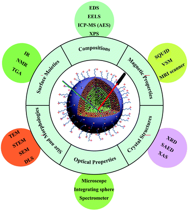
In this review, we focus on state-of-the-art techniques used to characterize UC nanocrystals, from surface structures to their intrinsic properties, namely surface moieties, crystal structures, sizes and morphologies, compositions, optical properties and magnetic characteristics (Fig. 1). In each section, we begin with a brief introduction of the physical principle of each technique, followed by data interpretation related to the properties of UC nanocrystals. The combination of different experimental techniques in the context of synergistic investigations of nano-phenomena in UC is also discussed. Driven by the promise of diverse and exciting applications, this field of research offers ultimate challenges in developing instruments for more precise characterization and better understanding of UC nanocrystals at single particle levels.
2. Characterization of surface moieties
The moieties on the surface of lanthanide-doped UC nanocrystals can be generally categorized into two classes: organic species and inorganic materials. The first type is widely utilized through conjugation or functionalization to provide control over the growth kinetics, size, and morphology of the inorganic core. The organic ligands can be further manipulated in the post-synthesis by ligand exchange,30 ligand oxidation,31 and layer-by-layer assembly,32 thereby offering a platform for facile functionalization of the UC nanocrystals. In contrast, the coatings of nanocrystals with inorganic moieties provide a pathway to chemically assemble more complex nanostructures, for example silica-modified core–shell structures for enhanced biocompatibility. Qualitative and quantitative characterization of the surface moieties present on the UC nanocrystals is an essential task after surface modification. A number of instrumentation techniques have been exploited to unveil the surface structures of UC nanocrystals, including IR, NMR and TGA. Note that the characterization of UC nanocrystals by TGA will not be reviewed herein and readers are referred to the literature for more information on this subject.2.1 IR spectroscopy
The IR technique is a simple but effective analytical tool to characterize ligand binding on the surface of UC nanocrystals. It is in the IR region of the spectrum in which various chemical groups in the molecule can be identified. Ligand molecules are constantly vibrating, and the energy levels corresponding to these motions mostly lie in the IR region, in the wavenumber range of 4000 to 200 cm−1. The combined use of the Fourier transform technique with an interferometer that comes with modern IR instruments makes all the required frequencies transmittable through the sample at once. A detector then records the interference pattern which is produced. Moreover, the availability of an attenuated total reflectance technique in conjunction with IR spectroscopy enables direct sampling in the solid or liquid state without further preparation, as well as improved spectral acquisition and reproducibility.33For illustration, let us consider the case of UC nanocrystals coated with ligands containing a carbonyl (C![[double bond, length as m-dash]](https://www.rsc.org/images/entities/char_e001.gif) O) group. Since the carbonyl group features a very intense absorption band at approximately 1700 cm−1, the validation of UC nanocrystals coated with ligands containing the carbonyl group can be achieved by the IR fingerprinting method. Note that the significant IR spectral bands of representative ligands used in the synthesis of UC nanocrystals are listed in Table 1. Particularly, oleic acids with absorption peaks at 2927 and 2857 cm−1 (stretching vibrations of –CH2), 1560 and 1464 cm−1 (stretching vibrations of –COO−), and 1705 cm−1 (stretching vibration of C
O) group. Since the carbonyl group features a very intense absorption band at approximately 1700 cm−1, the validation of UC nanocrystals coated with ligands containing the carbonyl group can be achieved by the IR fingerprinting method. Note that the significant IR spectral bands of representative ligands used in the synthesis of UC nanocrystals are listed in Table 1. Particularly, oleic acids with absorption peaks at 2927 and 2857 cm−1 (stretching vibrations of –CH2), 1560 and 1464 cm−1 (stretching vibrations of –COO−), and 1705 cm−1 (stretching vibration of C![[double bond, length as m-dash]](https://www.rsc.org/images/entities/char_e001.gif) O) have proven valuable for the controlled synthesis of lanthanide-doped nanocrystals. The use of oleic acids with a boiling point of 360 °C typically favors the preparation of high quality nanocrystals requiring treatment at elevated temperatures in the range of 290 to 310 °C.63 Importantly, the long alkyl chain of the oleate ligands and the strong binding affinity between the carboxyl group and the lanthanide ions at the surface of the UC nanocrystals render the as-synthesized nanomaterials with excellent dispersibility in non-polar solvents such as chloroform, hexane and cyclohexane. Notably, the oleate ligands can be removed from the particle surface after acid treatment.64 The removal of the oleate ligand can be spectroscopically confirmed by the disappearance of alkene and carboxylate stretching peaks at 3004 and 1564 cm−1, respectively.64 Fourier transform IR spectroscopy can also be applied to the characterization of inorganic coatings made of silicon oxide and carbon on the basis of their characteristic absorptions in the IR region (Si–O–Si: stretching vibration at 1100 cm−1; O–H: stretching vibration at 3320 cm−1; C–OH: stretching vibration at 1000–1300 cm−1). As a separate note, the amination of silica-coated UC nanocrystals is perhaps the most reliable strategy to introduce amine functional groups for chemical bonding with biomolecules such as protein, DNA and peptide.56–60
O) have proven valuable for the controlled synthesis of lanthanide-doped nanocrystals. The use of oleic acids with a boiling point of 360 °C typically favors the preparation of high quality nanocrystals requiring treatment at elevated temperatures in the range of 290 to 310 °C.63 Importantly, the long alkyl chain of the oleate ligands and the strong binding affinity between the carboxyl group and the lanthanide ions at the surface of the UC nanocrystals render the as-synthesized nanomaterials with excellent dispersibility in non-polar solvents such as chloroform, hexane and cyclohexane. Notably, the oleate ligands can be removed from the particle surface after acid treatment.64 The removal of the oleate ligand can be spectroscopically confirmed by the disappearance of alkene and carboxylate stretching peaks at 3004 and 1564 cm−1, respectively.64 Fourier transform IR spectroscopy can also be applied to the characterization of inorganic coatings made of silicon oxide and carbon on the basis of their characteristic absorptions in the IR region (Si–O–Si: stretching vibration at 1100 cm−1; O–H: stretching vibration at 3320 cm−1; C–OH: stretching vibration at 1000–1300 cm−1). As a separate note, the amination of silica-coated UC nanocrystals is perhaps the most reliable strategy to introduce amine functional groups for chemical bonding with biomolecules such as protein, DNA and peptide.56–60
| UC nanocrystals | Surface ligand or coating | Characteristic absorption (cm−1) | Remarks | Ref. | |
|---|---|---|---|---|---|
| a PAA: poly(acrylic acid). b PVP: polyvinylpyrrolidone. c PEI: polyethylenimine. d EDTA: ethylenediaminetetraacetic acid. | |||||
| Hydrophobic ligands |
LaF3:Yb/Ho(Tm)
NaYF4:Yb/Er NaYbF4:Er |
Oleic acid | 2927 and 2857; 1560 and 1464; 1705 | Asymmetric and symmetric stretching vibrations of –CH2 and –COOH; stretching vibration of C![[double bond, length as m-dash]](https://www.rsc.org/images/entities/char_e001.gif) O O |
34–36 |
|
NaYF4:Yb/Er(Tm)
LaF3:Yb/Er |
Oleylamine | 3007; 2926 and 2855; 1098 and 1564 | Stretching vibration of ![[double bond, length as m-dash]](https://www.rsc.org/images/entities/char_e001.gif) C–H; asymmetric and symmetric stretching vibrations of –CH2; stretching and deformation vibration of C–N and –NH2 C–H; asymmetric and symmetric stretching vibrations of –CH2; stretching and deformation vibration of C–N and –NH2 |
37, 38 | |
| NaYF4:Yb/Er | Oleic acid-trioctylphosphine | 2940; 1720 | Asymmetric and symmetric stretching vibrations of –CH2; stretching vibration of C![[double bond, length as m-dash]](https://www.rsc.org/images/entities/char_e001.gif) O O |
39, 40 | |
| Hydrophilic ligands |
YF3:Yb/Er
NaYF4:Yb/Er(Tm) |
PAAa | 3491; 1732 and 1422; 1571 and 1461 | Vibration of O–H; stretching vibration of C![[double bond, length as m-dash]](https://www.rsc.org/images/entities/char_e001.gif) O and C–O; asymmetric and symmetric stretching vibrations of –COO− O and C–O; asymmetric and symmetric stretching vibrations of –COO− |
41–43 |
| NaYF4:Yb/Er(Tm) | PVPb | 2958 and 2847; 1651; 1445 | Asymmetrical and symmetrical stretching vibrations of CH2; stretching vibration of C![[double bond, length as m-dash]](https://www.rsc.org/images/entities/char_e001.gif) O; bending vibration of CH2 O; bending vibration of CH2 |
30, 44–46 | |
| NaYF4:Yb/Er(Tm) | PEIc | 3436; 1638 and 750; 2930 and 2861 | Stretching vibration of O–H or N–H; bending vibration of N–H; asymmetric and symmetric stretching vibrations of –CH2 | 47–50 | |
| BaYF5:Yb/Er(Ho,Tm) | EDTAd | 1374 | Stretching vibration of C![[double bond, length as m-dash]](https://www.rsc.org/images/entities/char_e001.gif) O (N–CO–OH) O (N–CO–OH) |
51 | |
|
NaYF4:Yb/Er
YVO4:Er |
Citrate | 2927 and 2850; 1610 and 1400 | Asymmetric and symmetric stretching vibrations of –CH2; stretching vibrations of –COOH | 33, 52–54 | |
| Inorganic coating | NaYF4:Yb/Er(Tm) | Amorphous C | 3320, 1000–1300 | Stretching vibration of O–H; vibration of C–OH groups | 55 |
| NaYF4:Yb/Er(Ho,Tm) BaYF5:Yb/Er | SiO2 | 1097 | Symmetrical stretching vibration of Si–O–Si | 30, 56–62 | |
| NaYF4:Yb/Er BaYF5:Yb/Er | SiO2–NH2 | 3423 and 1637 | Stretching and bending vibrations of N–H | 56–60 | |
It is important to emphasize that the presence of surface ligands may suppress the UC emission of the nanocrystals as opposed to the naked nanocrystals. This phenomenon is known as surface quenching effects, as surface ligands can participate in non-radiative relaxation via stretching vibration of chemical bonds. For example, it was found that the ultraviolet emission intensity of NaGdF4:Yb/Tm@NaGdF4 nanocrystals at 290 nm increased substantially after the removal of the oleate ligands.65 The alkyl chain length of the ligands can be correlated well to the surface quenching effect because the trapping of the excitation energy dominates in the ligands containing more methylene units.66 The emission by surface moieties has been reported from surface-capped UC nanocrystals upon excitation at 980 nm as a result of Föster resonance energy transfer between the emissive particle and the ligands at the surface.29,65,67
In some circumstances, IR analysis can be utilized to understand abnormal optical properties of UC nanocrystals by monitoring the chemical reactions between the ligands. For example, Wu and co-workers demonstrated that amidation reaction can proceed in a mixed solvent of oleic acid and octadecylamine at 250 °C (Fig. 2a).68,69 The generation of N-octadecyloleamide was confirmed by the appearance of two characteristic absorption peaks at 1635 and 1536 cm−1 corresponding to C![[double bond, length as m-dash]](https://www.rsc.org/images/entities/char_e001.gif) O stretching and N–H bending vibrations, respectively. Importantly, the vibrational energy of the in situ generated molecule matches well with the energy gap between 2H11/2 (or 4S3/2) → 4F9/2 (∼3000 cm−1) and 4I11/2 → 4I13/2 (3300 cm−1) transitions of Er3+, resulting in an enhanced red emission from NaYF4:Yb/Er (20/2 mol%) nanocrystals (Fig. 2b).69
O stretching and N–H bending vibrations, respectively. Importantly, the vibrational energy of the in situ generated molecule matches well with the energy gap between 2H11/2 (or 4S3/2) → 4F9/2 (∼3000 cm−1) and 4I11/2 → 4I13/2 (3300 cm−1) transitions of Er3+, resulting in an enhanced red emission from NaYF4:Yb/Er (20/2 mol%) nanocrystals (Fig. 2b).69
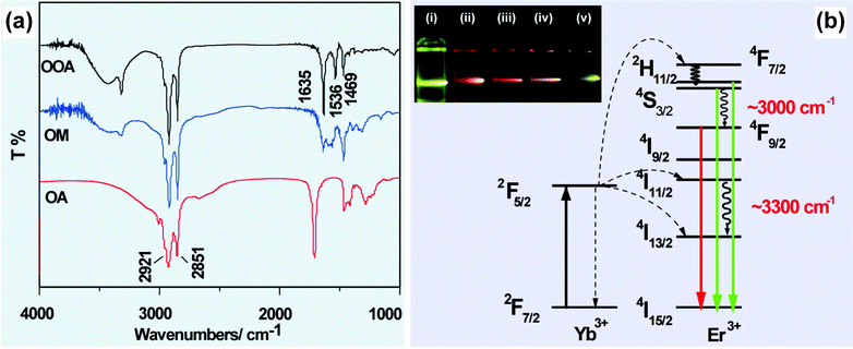 | ||
| Fig. 2 FTIR characterization for elucidating IR absorptions on UC emission of lanthanide-doped nanocrystals. (a) FTIR spectra of oleic acid (OA), octadecylamine (OM) and N-octadecyloleamide (OOA). (b) Schematic illustration of the generation of enhanced red emission from N-octadecyloleamide (OOA)-capped NaYF4(NaGdF4):Yb/Er (20/2 mol%) nanocrystals. Note that the inserted photo shows luminescent images of NaGdF4:Yb/Er (20/2 mol%) nanocrystals prepared using different molar ratio of oleic acid/octadecylamine: (i) 0/55; (ii) 5/50; (iii) 20/35; (iv) 35/20; (v) 55/0. (Reprinted with permission from ref. 69. Copyright 2011, Royal Society of Chemistry.) | ||
Although valuable for qualitative and structural analysis, the IR-based technique is seldom used for quantitative analysis of surface ligands on the nanocrystals, partly because it is difficult to obtain accuracy of intensity measurement. The IR technique is also insensitive to chemical environment, implying the difficulty in unraveling the origin of absorption peaks. For instance, it is impossible to attribute the asymmetric and symmetric stretching vibrations of –CH2– to particle-tethered oleic acid or oleylamine. Moreover, the exact nature of ligand binding is hard to determine by the IR method, especially for covalently attached molecules and non-specifically adsorbed ones.
2.2 NMR spectroscopy
Perhaps the chemist's favorite structural analytical tool is NMR spectroscopy. Basically, NMR is concerned with atomic nuclei having a property called ‘spin’ which gives them magnetic properties. The spin quantum number of the nuclei can be correlated to their shapes. For example, spherical shaped nuclei have a spin of 1/2, and those with other shapes have a value of 1 or more.70 Nuclei with a spin number of 1/2 can split into two states, namely +1/2 and −1/2, in the presence of an external magnetic field. If electromagnetic radiation of radio frequency is applied to the sample, some of these nuclear magnets can absorb energy and convert the low spin state (+1/2) to a higher one (−1/2).Recently, an NMR technique has been developed as a powerful tool for the characterization of organic species immobilized on inorganic nanoparticles, such as quantum dots and UC nanocrystals.71–73 The increased line broadening is one of the problems associated with NMR studies on particle-tethered ligands due to inhomogeneity in chemical environment and limited rotational freedom of the ligands. For example, a series of 1H NMR chemical shifts from oleic acid-coated NaYF4 nanocrystals were detected in regions ranging from 0.85 to 5.45 ppm (Fig. 3).71–73 As the size of the particle increases, the NMR spectrum becomes even more crowded with overlapping signals – to an extent where the resolution of the peak separation becomes untenable. The shifting in NMR signals is another representative characteristic of the ligands anchored on the surface of UC nanocrystals because the nanoparticle can significantly shield the magnetic nucleus from the external field. A typical example is the observation of the chemical shift in oleylamine from 2.64 to 2.68 ppm due to the presence of the nanoparticle.74
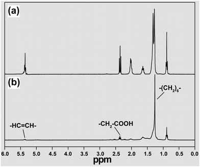 | ||
| Fig. 3 Characterization of ligand-capped UC nanocrystals by NMR spectroscopy. The 1H NMR spectra of (a) free oleic acid and (b) oleic acid-modified NaYF4 nanocrystals in CDCl3 recorded on a Varian 300 MHz spectrometer. Note that undoped NaYF4 nanocrystals were investigated instead of doped ones to exclude the intrinsic effect of magnetic disturbances arising from lanthanide dopants. (Reprinted with permission from ref. 72. Copyright 2007, American Chemical Society.) | ||
NMR depends on the magnetic properties of certain nuclei and subtle alteration of their chemical environment. As a representative instrument tool for surface ligand characterization, NMR is sensitive to the changes in ligands attached on the surface of UC nanocrystals. For example, 1H NMR signals of –HC![[double bond, length as m-dash]](https://www.rsc.org/images/entities/char_e001.gif) CH– (at 5.34 ppm) and –CH3 (at 0.85 ppm) of oleic acid disappeared after chemical transformation to azelaic acid via Lemieux–von Rudloff oxidation.321H NMR signals at 5.34 ppm were also absent when hydroxylation reaction was conducted on the carbon–carbon double bond.75 When oleate-capped UC nanocrystals were treated with strong acid to remove surface ligands, all 1H NMR signals vanished.64,76,77
CH– (at 5.34 ppm) and –CH3 (at 0.85 ppm) of oleic acid disappeared after chemical transformation to azelaic acid via Lemieux–von Rudloff oxidation.321H NMR signals at 5.34 ppm were also absent when hydroxylation reaction was conducted on the carbon–carbon double bond.75 When oleate-capped UC nanocrystals were treated with strong acid to remove surface ligands, all 1H NMR signals vanished.64,76,77
NMR is also a reliable tool to monitor the reactions between the ligands to elucidate their “cooperative effect” on size and morphology control, phase transition, and color output of UC nanocrystals. 1H NMR signals of NaYF4:Yb/Er (20/2 mol%) nanocrystals synthesized in a mixture of oleic acid and octadecylamine matched well with that of oleamide, evidencing the occurrence of inter-ligand reaction in the synthesis.69,74 The generated oleamide resulted in the synthesized UC nanocrystals with an enhanced red emission.69 In a recent study, Cohen and co-workers reported that the in situ generated oleamide promoted the formation of hexagonal phase NaYF4:Yb/Er (20/0.2 mol%) nanocrystals due to its neutral characteristic.78 In another parallel experiment, the NMR analysis of 1H and 31P verified the formation of oleate–trioctylphosphine during the synthesis of UC nanocrystals in a mixed solvent at 315–320 °C. The in situ formed ligands are capable of reducing energy barrier in cubic-to-hexagonal phase transformation, facilitating the formation of bright hexagonal phase NaYF4:Yb/Er (20/2 mol%) nanocrystals.79
Although the NMR technique has been successfully applied to characterize surface ligands anchored on the surface of quantum dots or plasmonic nanocrystals, this technique oftentimes suffers from a significant line broadening of the NMR signals in the case of UC nanocrystals, arising mainly from intrinsic paramagnetic properties of many lanthanide dopants, such as Gd3+, Er3+ and Ho3+.38 One solution for probing the ligands bound to the surface of UC nanocrystals is to measure the undoped counterparts to exclude the effects of paramagnetic disturbances.69,74,80 When an excess of free ligand was present in solution, rapid exchange of ligands may impose additional challenges in the precise characterization of the particle surface ligands by NMR spectroscopy.
3. Identification of crystal structures
Crystal structure is perhaps one of the most significant parameters that affect the energy transfer efficiency between lanthanide dopants in the host lattices as the choice of the crystal structure dictates the coordination number, the distance between dopant ions and their relative spatial position. These factors give rise to different probabilities in f–f transition of the lanthanide activators, accounting for tunable optical properties of UC nanocrystals. Low symmetry of lanthanide-doped hexagonal NaYF4 leads to an efficiency of UC up to ten times higher than that of its cubic counterpart.81 Recently, Wang et al. discovered that the packing manner of lanthanide ions in the crystal lattice can also influence the energy transfer efficiency between Yb3+ and Er3+.82 Tetrad clustering of Yb3+ ions favors preservation of excitation energy and thus enhances energy transfer from Yb3+ to Er3+, enabling the generation of an unusual violet emission at 410 nm of Er3+ in orthorhombic-phase KYb2F7.82 In this section, we highlight the utilization of two characterization techniques, based on powder XRD and XAFS spectroscopy, for the structural characterization of UC nanocrystals. The method of electron diffraction will be emphasized in the section of TEM characterization.3.1 Powder XRD
The non-destructive nature and relative ease of sample preparation make powder XRD a widespread technique used for structure determination of UC nanomaterials. The diffraction of scattered X-rays by crystalline materials is depicted in Fig. 4a and b. When the difference in the path-length of the scattered X-rays is an integral number of wavelength of incident X-rays, the X-rays will interact with each other to yield a constructive interference. This phenomenon is known as Bragg's Law (eqn (1)):nλ = 2d![[thin space (1/6-em)]](https://www.rsc.org/images/entities/char_2009.gif) sin sin![[thin space (1/6-em)]](https://www.rsc.org/images/entities/char_2009.gif) θ θ | (1) |
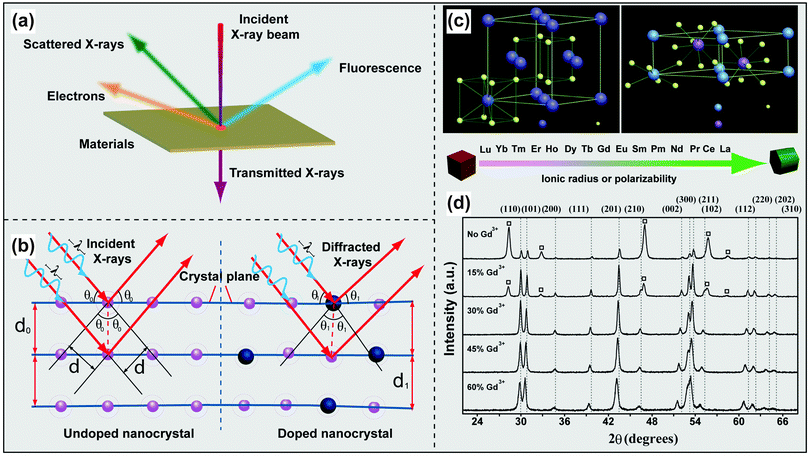 | ||
| Fig. 4 Characterization of lanthanide-doped UC nanocrystals by XRD techniques. (a) Schematic illustration of the interaction of X-rays with a thin film material. (b) Different diffractions of scattered X-rays scattered by undoped and doped atomic planes. (c) Schematic presentation of cubic- and hexagonal-phase NaREF4 structures and general trend of phase transition from cubic to hexagonal as a function of ionic radius (or polarizability) of the lanthanide dopant ions. (d) Representative XRD patterns of NaYF4:Yb/Er (18/2 mol%) nanocrystals with different levels of Gd3+ doping. The diffraction patterns arising from cubic NaYF4 are marked with square boxes. (Reprinted with permission from ref. 17. Copyright 2010, Nature Publishing Group.) | ||
The diffraction angle and intensity are highly sensitive to crystal structures, thereby enabling the identification of crystallinity of UC nanocrystals to be readily identified by comparing the diffraction patterns with well-established database (standard powder diffraction card of Joint Committee on Powder Diffraction Standards). Strong diffraction peaks are commonly observed from high quality lanthanide-doped UC nanocrystals adopting a hexagonal or cubic phase. These nanocrystals were generally prepared at high reaction temperatures (200 to 300 °C) by various methods, including coprecipitation, hydrothermal treatment, and thermal decomposition.17,83
XRD techniques can also be used to monitor the phase transformation of NaREF4 (RE: rare-earth ion) nanocrystals. For example, the addition of Gd3+ ions to NaYF4 precursors renders great control over the phase of the resultant UC nanocrystals as evident by XRD measurements (Fig. 4c and d).17 Zeng et al. reported a similar role of Gd3+ in the synthesis of NaLuF4:Gd/Yb/Tm nanocrystals and found that the presence of Gd3+ can promote the rate of cubic-to-hexagonal phase transformation and facilitate the formation of small-sized UC nanocrystals.84 XRD characterization confirmed the reversed phase transformation of NaREF4 (RE: Lu, Gd, Yb) from hexagonal to cubic by insertion of transition metal dopants (e.g., Mn2+) into the host lattice.85,86 Doping of small-sized alkaline metal ions into RE-based host lattices is also effective for phase control as demonstrated by Dou and Zhang.87 In their study, they showed that hexagonal-phase NaYF4 nanoparticles were first converted to cubic ones and further to tetragonal counterparts with increasing dopant concentration of Li+.87 Critically, doping of impurities can distort the local symmetry of lanthanide dopants or lead to the variation in energy transfer pathways, thus providing a facile platform to manipulate the optical properties of UC nanocrystals.88,89
XRD investigations also provide additional valuable information on UC nanocrystals such as size, lattice strain, and morphology. Appreciable line broadening in diffraction patterns typically indicates a decrease in the size of the particles. Scherrer's equation (eqn (2)) is usually applied to estimate the average size of UC nanocrystals when the stress in crystallites is not taken into consideration.22,71,90
 | (2) |
 | (3) |
![[thin space (1/6-em)]](https://www.rsc.org/images/entities/char_2009.gif) cos
cos![[thin space (1/6-em)]](https://www.rsc.org/images/entities/char_2009.gif) θ/λ against sin
θ/λ against sin![[thin space (1/6-em)]](https://www.rsc.org/images/entities/char_2009.gif) θ/λ.92 Recently, tensile (positive sign) and compressive strain (negative sign) were observed in LaPO4:Yb/Tm and core–shell LaPO4:Yb/Tm nanoparticles, respectively.93 It should be noted that a number of factors, including doping, thermal annealing and shell-coating, can induce lattice strain in the nanosized crystals. Considering that the lattice strain (or local compressive stress) has a marked impact on the optical and electronic properties of colloidal semiconducting nanocrystals and photophysical properties of dye molecules,94,95 the study of line broadening by XRD techniques can be used to elucidate the correlation between lattice strain and UC processes in lanthanide-doped nanocrystals.96,97
θ/λ.92 Recently, tensile (positive sign) and compressive strain (negative sign) were observed in LaPO4:Yb/Tm and core–shell LaPO4:Yb/Tm nanoparticles, respectively.93 It should be noted that a number of factors, including doping, thermal annealing and shell-coating, can induce lattice strain in the nanosized crystals. Considering that the lattice strain (or local compressive stress) has a marked impact on the optical and electronic properties of colloidal semiconducting nanocrystals and photophysical properties of dye molecules,94,95 the study of line broadening by XRD techniques can be used to elucidate the correlation between lattice strain and UC processes in lanthanide-doped nanocrystals.96,97
The success of lanthanide doping in UC nanocrystals can be directly measured by the shift of the diffraction lines in the patterns. The position of the diffraction line is strongly sensitive to the d-spacing of scattering atomic planes according to Bragg's Law. Substantial alteration of d-spacing may be affected by different sized impurities as a result of unit cell shrinkage or expansion (Fig. 4b). For instance, the replacement of Na+ or Y3+ by small-sized Li+ or Mn2+ in cubic NaYF4 host lattice results in shifting of diffraction lines to a higher angle,85,87,88 while big-sized dopants (e.g., Gd3+ and K+) give rise to lower-angle shifting of the diffraction patterns.17,87,98 However, these two opposite effects can offset each other in some cases, generating negligible shifting in the diffraction patterns of doped UC nanocrystals. As revealed by Wang's group in XRD analysis of Ca2+-doped NaGdF4,99 the expanding effect on cell volume by incorporating large-sized Ca2+ is counterbalanced by the formation of F− vacancies.
Anisotropic line broadening observed in the XRD characterization of UC nanocrystals can provide useful information on the morphology of the nanocrystals.100 Theoretically, samples with homogeneous distribution and completely random orientation are required for XRD measurements. Different shaped nanocrystals usually display slightly different diffraction patterns in terms of intensity and anisotropic line broadening.101–103 Spherical and rod-shaped UC nanocrystals typically show enhanced (h00) but diminished (002) reflections, while a reverse trend is observed for hexagonal nanoprisms and nanoplates.103 Abnormal strong diffraction lines can also provide clues on preferential growth directions of the nanoparticle.104 For example, strong diffraction intensity from (100) planes of NaYF4 microcrystals manifests the preferential growth along the [001] crystallographic direction.105,106
XRD techniques can provide compositional mapping of parts of a crystalline species with a weight fraction of larger than 3%. With synchrotron radiation, the sensitivity can be improved down to 0.05% (500 ppm). The low detection limit of XRD clearly makes it difficult to characterize heterostructured or multi-phased nanocrystals in which one component significantly outweighs the others.107–109 Despite the usefulness of the Rietveld refinement for quantitative analysis of NaYF4 nanocrystals with a mixture of cubic and hexagonal phases, the content of the examination component must be larger than 8%.78 This aspect is not trivial and can lead to serious errors if improperly performed.
3.2 XAS
XAS spectroscopy, based on the X-ray photoelectric effect and the wave nature of the electron, can be used to determine local structures around a specific dopant atom. Unlike X-ray diffraction, it places few constrains on the samples and works equally well in amorphous materials, liquids, and polycrystalline solids. The X-ray absorption spectrum is typically classified into two groups: X-ray absorption near-edge spectroscopy (XANES) and extended X-ray absorption fine-structure spectroscopy (EXAFS). XANES is strongly sensitive to formal oxidation state and coordination geometry of the absorbing atom, while the EXAFS is used to provide information about interatomic distances and the coordination number of the absorbing atom.EXAFS is a powerful technique for determining the chemical state of lanthanide dopants which occur in very low concentration. For example, Song's group demonstrated that the changes in the Er–O bond length and the coordination number of Er in ZnO:Er nanocrystals, induced by Li+ doping, can be measured by means of EXAFS.110 In a parallel development through use of EXAFS, Liu et al. confirmed that incorporation of Li+ ions into the interstitial sites of Y2O3:Er3+ nanoparticles results in a notable enhancement in Er3+ emission as a result of its reduced symmetric environment.111
As EXAFS focuses on the local structure of a given chemical species irrespective of long range order, it is a versatile tool to correlate the UC emission to the local environment of lanthanide dopants, thereby providing valuable data for rational design of UC nanocrystals with precisely controlled emissions. Chang and co-workers modeled the structure of Y2O3:Er3+ nanocrystals on the basis of EXAFS data and further correlated the results through Judd–Ofelt analysis.112 They found that both approaches match well with each other in predicting optimal doping concentrations of Er3+ for core (5 mol%) and core–shell (2 mol%) nanocrystals. Low limits of detection down to ppm are another notable merit of this technique with synchrotron X-rays as the light source, allowing the UC nanocrystals to be analyzed even at an extremely low dopant concentration. It should be noted that to make the fitting results from XAFS more reliable, the samples should have high homogeneity.
4. Determination of size and morphology
Size and morphology are important factors that affect the optical properties of UC nanocrystals with respect to relative emission intensity (e.g., the green-to-red emission ratio of Er3+), quantum yield, and lifetime.113–115 Both factors also have a significant impact on the performance of UC nanocrystals in nanomedicine concerning the circulation lifetime, cell surface barrier penetration ability, and cell uptake effectiveness. For example, bright UC nanocrystals with diameters smaller than 10 nm are more attractive in bioimaging or biolabeling than their large-sized equivalents.116 In addition, the shape of UC nanocrystals should be taken into consideration when they are exploited as building blocks to fabricate multifunctional solids.117 Morphology-directed assembly into mesoscopic superlattices was observed in the case of NaYF4:Yb/Er (20/2 mol%) nanocrystals or tripodal Gd2O3 nanoplates.103,118 Shape-complementary effects of rhombic GdF3 and tripodal Gd2O3 nanoplates were recently disclosed in the formation of highly ordered superlattices.119 In this section, typical electron microscopes, including TEM, STEM and SEM that use a beam of electrons to construct the specimen image, are introduced and compared for characterizing UC nanocrystals.The development of electron microscopy techniques has been fueled by their ability to visualize ultra-small objects invisible by conventional light microscopes. Electron microscopy operates based on the interaction between the electrons and the materials under investigation. A series of signals such as transmitted electrons, backscattered electrons, secondary electrons, Auger electrons and characteristic X-rays are generated, allowing rather comprehensive characterizations of the materials in terms of size, structure, morphology, and composition. As the availability of parallel electron beams in TEM, the use of electron diffraction for studying the crystal structure of UC nanocrystals is also described in this section.
4.1 TEM imaging
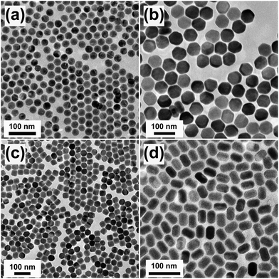
TEM can be used as a direct tool to reveal the morphology of lanthanide-doped UC nanocrystals prepared under different synthetic conditions (Fig. 5). Precise growth habits of lanthanide-doped materials under a certain condition are predicable by screening morphology changes in response to varied synthetic conditions. For example, the growth of a conformal anisotropic shell on a nanocrystal core can be modulated by the ligand etching effect and the strain induced by the lattice mismatch between the core and shell materials.120 With the help of TEM characterization, Zhang et al. validated an end-on growth mechanism responsible for the growth of multicolor-banded crystals.121 Another demonstration of utility of TEM for analyzing an epitaxial layer-by-layer growth on NaYF4 UC nanocrystals was reported by van Veggel's group.122 In their work, Ostwald ripening dynamics was utilized to yield core–shell structured nanocrystals.Phase contrast methods of high-resolution imaging offer better spatial resolution than conventional TEM imaging. The diffraction contrast (brightness) from crystalline interfaces due to incident electron scattering difference often contains rows of one-dimensional bands or fringes, which can be used to examine the formation of heterostructures in UC nanocrystals. For example, different components in NaYF4:Yb/Er-CdSe, NaYF4:Yb/Tm-Au and NaYF4:Yb/Er@SiO2 nanocrystals can be differentiated clearly thanks to the contrast differences in TEM images.61,123–125 For NaYF4@NaGdF4 nanoparticles, the structure and chemical composition at the core–shell interface can hardly be distinguished by this imaging technique as the core and shell components have similar capability of scattering incident electrons. Under these circumstances, the formation of core–shell nanostructures via seed-mediated growth methods can be indirectly identified by measuring the average size of the nanocrystals, the enhancement in emission intensity, and the change in the emission lifetime and quantum yield.126,127
Under a high-resolution imaging mode, the crystallographic structures of UC nanocrystals, including crystalline defects and crystallite domains, can be inspected at an atomic level (Fig. 6a and b).65,126 Interface-specific inspection for UC nanocrystal-based heterodimers provides important information on the growth mechanism, laying the foundation for the fabrication of multimodal imaging agents.107,128,129 Much detailed analysis of UC nanocrystals is often performed with a phase-amplitude diagram – a graphical construction of a complex Fourier transform.82 Typically, a refined-HRTEM image is utilized to construct a corresponding symmetry-imposed image. The amplitude and phase are extracted from the lattice position of the Fourier transform and analyzed against the different plane groups using professional image processing programs. Using this approach, quantitative analysis of K, Yb and F atoms in the KYb2F7:Er lattice can be obtained as shown in Fig. 6c.82 It is worth noting that TEM can also be operated in the scanning mode, known as STEM, to perform point-by-point scanning across samples using a focused electron probe. The STEM technique offers impressive imaging resolution down to sub-Ångstrom under an accelerating voltage of 300 kV, thereby enabling to resolve single atoms as demonstrated in a NaGdF4:Yb/Tm@NaGdF4:Tb core–shell nanocrystal (Fig. 6d).65
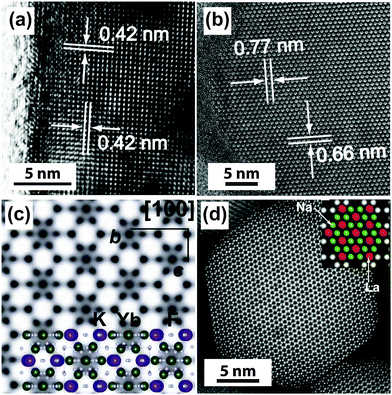 | ||
| Fig. 6 High-resolution TEM/STEM characterization of UC nanocrystals. (a) HRTEM image of a KMnF3:Er (10 mol%) nanobelt (unpublished results). (b and c) HRTEM images of a KYb2F7:Er (2 mol%) nanocrystal and the corresponding symmetry-imposed image. (d) High-resolution STEM image of a NaGdF4:Yb/Tm (49/1 mol%)@NaGdF4:Tb (15 mol%) core–shell nanocrystal. Note that due to the high resolution capability of HRTEM and STEM, the location of lanthanide and sodium atoms can be identified by both techniques as indicated in the insets of (c) and (d). (Reprinted with permission from ref. 65 and 82. Copyright 2014 and 2011, Nature Publishing Group.) | ||
A unique feature of UC nanocrystals is their relatively low thermal stability under electron beam irradiation, thus posing a challenge in acquiring high quality HRTEM images.130 Yan and co-workers irradiated a single NaYF4:Yb/Er nanoparticle with a spark of an electron beam for an extended time period and observed in situ solid-to-hollow transformation of the particle (Fig. 7).131 Gao and co-workers attributed this phase transition to a cooperative result of knock-on effects, specific lattice strain and low surface energy associated with NaREF4 nanomaterials.132 Johnson et al. recently highlighted that the stability of coreshell UC nanocrystals on high-dose irradiation is closely related to the interfacial strain.133 Tensile-force-shelled UC nanocrystals, such as NaYF4@NaTmF4, exhibited a deleterious stability as opposed to their compress-shelled equivalents (e.g., NaYF4@NaDyF4). These findings may provide an intriguing strategy to pattern lanthanide-doped nanocrystals by electron beam manipulation. One promising way of minimizing the overheating effect is to use cryogenic TEM for reliable sample analysis as suggested by Zhao and co-workers.134
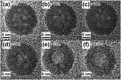 | ||
| Fig. 7 Morphologic evolution of a hexagonal-phase NaYF4:Yb/Er (20/2 mol%) nanocrystal under electron beam irradiation at different time intervals. (a–f) 0, 15, 30, 60, 90 and 120 s, respectively. (Reprinted with permission from ref. 131. Copyright 2009, Wiley-VCH Verlag GmbH & Co. KGaA.) | ||
As an added benefit, TEM provides imaging capability of SAED on individual UC nanocrystals by taking advantage of electromagnetic lens and physical apertures. Phase-specific patterns of dots in single-crystal structures have been observed in the SAED measurement of Gd3+-doped NaYF4, Er3+-doped NaYbF4, NaYF4:Yb/Er and NaYF4:Yb/Ho/Tm nanocrystals.17,128,129,135,136 Moreover, combining the results of HRTEM with SAED data performed on single nanocrystals can provide valuable information on the growth direction of NaYF4:Yb/Er (18/2 mol%) nanowires.137
A powder diffraction pattern, similar to the case of powder XRD, can be generated when a large number of nanocrystals are illuminated by an electron beam (Fig. 8a and b).26,116,138–140 The diameter (D) of the ring in the powder pattern can be derived from eqn (4), where d refers to lattice spacing of a specific scattering atomic plane, λ is the wavelength of the electron beam, and L is the effective camera length of the electron microscope.
 | (4) |
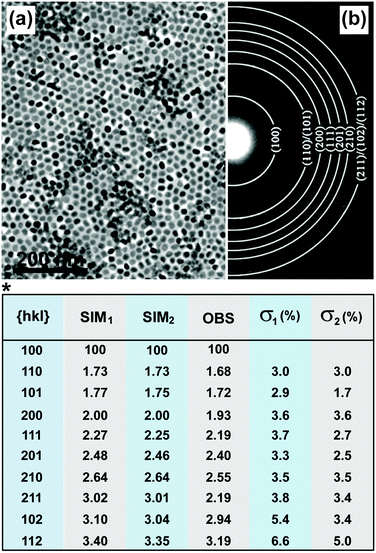 | ||
| Fig. 8 Characterization of UC nanocrystals by SAED. (a) TEM image of NaYF4:Yb/Er (20/2 mol%)@NaGdF4 nanocrystals and (b) corresponding powder patterns of the nanocrystals by SAED characterization. (*) Comparison of observed relative ring spacing (d-spacing) (OBS) and stimulated values on the basis of bulk NaYF4 (SIM1) and NaGdF4 (SIM2) crystals. The deviation between the experimental data (NaYF4:Yb/Er@NaGdF4 nanocrystals) and SIM (bulk NaGdF4 and NaYF4 crystals) values for each set of miller indices (hkl values) were quantitative evaluated in terms of σ value. σ1 = (SIM1 − OBS)/OBS; σ2 = (SIM2 − OBS)/OBS. (Reprinted with permission from ref. 134. Copyright 2012, American Chemical Society.) | ||
A number of factors, such as doping or shell coating, principally give rise to changes in the d-spacing (Fig. 8, table). It should be noted that the detection sensitivity of SAED is lower than that of XRD because of errors possibly induced by specimen defects, the aberrations of a given electromagnetic lens, and limitations in connection with the recording systems.
SAED is an extremely useful technique for providing information on the packing order of the nanoparticles upon aggregation.141 Murray and co-workers reported the observation of single crystal-like diffraction patterns from superlattices of anisotropic UC nanocrystals. The single crystal-like diffraction patterns implies highly ordered packing in position and orientation of the nanocrystal building blocks.103 For SAED measurements, it is worth noting that the specimen under examination should be thin (typically less than 100 nm) to reduce the inelastic scattering of the incident electron beam, allowing reflection spots to be generated in the diffraction patterns.
4.2 STEM imaging
Apart from high imaging resolution, STEM in a high-angle annular dark-field (HAADF) imaging mode is a terrific technique that can be used to distinguish the interfacial region of a core–shell UC nanocrystal. This capability stems from the fact that heavy atoms tend to generate high-angle scattered electrons and the contrast difference obtained by HAADF-STEM imaging of different components in a nanocrystal is proportional to the square of Z (Z = atomic number).142 Different layers in a variety of core–shell or multilayer core–shell UC nanocrystals have been characterized by the HAADF-STEM imaging technique, including NaYF4@NaGdF4, NaGdF4:Yb/Ca/Er@NaYF4, NaYbF4:Tm@CaF2, and NaGdF4:Nd@NaYF4@NaGdF4:Nd/Yb/Er (Fig. 9).99,127,134,143,144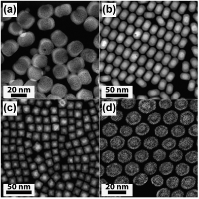 | ||
| Fig. 9 HAADF-STEM for effectively differentiating the core and shell layers of UC nanocrystals. (a) NaYF4@NaGdF4. (b) NaGdF4:Yb/Ca/Er@NaYF4. (c) NaYbF4:Tm@CaF2. (d) NaGdF4:Nd@NaYF4@NaGdF4:Nd/Yb/Er. (Reprinted with permission from ref. 99, 127, 143 and 144. Copyright 2011, 2013, 2012 and 2013, American Chemical Society, Royal Society of Chemistry and Nature Publishing Group.) | ||
Despite a number of excellent capabilities, the STEM imaging technique has inherent limitations and problems, some of which are associated with the low thermal stability of lanthanide-doped nanocrystals in response to electron beam irradiation. Similar to the mitigation measure adopted by TEM, the damage to the nanocrystals in STEM mode can be largely reduced by imaging the nanocrystals at a low temperature of 96 K.134 Notably, the scanning mode of STEM is attractive in analyzing the spatial distribution of elements in a nanocrystal which will be described in the section of composition analysis.
4.3 SEM imaging
SEM is a convenient method for high resolution imaging of surfaces. The advantages of SEM over STEM include great depth of field and 3D rendering opportunity albeit their similarity in the operating mechanism. SEM utilizes secondary electrons, or backscattered electrons or a mixture of both types of electrons for imaging. As the signals can be generated from the surface layer of the specimen from several to 100 nm in depth contingent on acceleration voltage, SEM provides a fertile ground for applications in characterizing the surface characteristics of small-sized UC crystals, such as flower-like β-NaYF4 hexagonal disks and NaYbF4 microtubes (Fig. 10a and b).106,145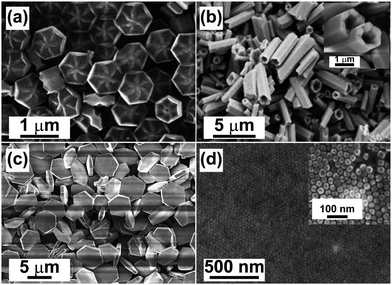 | ||
| Fig. 10 SEM characterization of lanthanide-doped UC crystals. (a) Flower-patterned hexagonal plates of NaYF4. (b) NaYbF4:Tm (1.0 mol%) microtubes. (c) NaYbF4 microplates (unpublished result). (d) NaYF4:Yb/Er (20/2 mol%) nanocrystal assemblies. (Reprinted with permission from ref. 106, 145 and 147. Copyright 2007, 2010, 2011 and 2009, Wiley-VCH Verlag GmbH & Co. KGaA, American Chemical Society and Royal Society of Chemistry.) | ||
With regard to drawbacks, the prevalent use of SEM under normal operating conditions for imaging small-sized UC nanocrystals is hindered by the charging effect due to low conductivity of the nanocrystals (Fig. 10c). Scanning faults and image artifacts resulting from the charging effect can be effectively minimized by coating the nanocrystals with a thin layer of a noble metal or carbon.101,102,105,145,146 Yan and co-workers found that by properly adjusting the acceleration voltage and imaging distance, the resolution of SEM could reach 20–30 nm for NaYF4:Yb/Er (20/2 mol%) nanoparticles without the surface coating (Fig. 10d).147,148
5. Composition determination
The concentration of the dopant in UC nanocrystals plays a very important role in determining the optical characteristics of the nanocrystals as non-radiative depopulation of activators highly depends on the level of doping. Consequently, UC nanocrystals with desirable optical features are achievable by deliberately optimizing doping concentration of sensitizers (Nd3+,Yb3+) and activators (Er3+,Ho3+,Tm3+).149,150 Presently, the dopant concentration of UC nanocrystals is typically estimated from the amount of the lanthanide precursors added to the solution, assuming that all the lanthanides are homogeneously doped into the nanocrystals after the reaction.23,24 However, one would expect a small discrepancy between predicted and observed values for the dopant concentration, partly introduced by a side reaction of the lanthanide precursors with the ligands (e.g., oleic acid). For example, Yan and co-workers found that the composition of NaYF4:Yb/Er nanocrystals varied with the reaction time via thermal decomposition of the lanthanide trifluoroacetate precursor.113 Yi and colleagues reported a similar phenomenon when preparing NaYF4:Yb/Er nanocrystals in the presence of ethylenediaminetetraacetic acid by a hydrothermal method.151 They ascribed the change in composition to different coordination abilities of lanthanides to EDTA, thus affecting the supersaturation and precipitation processes key to the formation of nanocrystals.In this section, we discuss instrumental techniques used to measure doping concentration of lanthanide ions in UC nanocrystals. Three general microanalytical techniques, EDS, EELS and XPS, will be first reviewed for their use in characterizing UC nanocrystals (Table 2). Then, we intend to highlight the application of ICP-MS and ICP-AES techniques for acquiring the dopant concentration of UC nanocrystals in bulk form.
| Technique | Incident illumination | Signals | Spatial resolution (nm) | Detection limit (atom%) | Single-particle characterization | Core–shell characterization | Ref. |
|---|---|---|---|---|---|---|---|
| a The parameters of EDS characterization are controlled by TEM imaging. Spatial resolution and detection limit of EDS by SEM are much lower than achievable by TEM. b The shell thickness should be less than 10 nm. | |||||||
| EDSa | Electron beam | X-ray | 1–10 | 0.1 | Yes | Yes | 65, 156 and 157 |
| EELS | Electron beam | Electron | 0.1–1 | 0.05 | Yes | Yes | 65, 134, 162 and 163 |
| XPS | X-ray | Electron | 5000–30![[thin space (1/6-em)]](https://www.rsc.org/images/entities/char_2009.gif) 000 000 |
0.01–0.5 | No | Yesb | 64, 124 and 164–168 |
5.1 EDS
EDS is an X-ray microanalytical technique that can provide information on the elemental composition of a sample upon bombarding of high energy electron beam. As a separate merit to TEM imaging, EDS is commonly used for elemental mapping of UC nanocrystals. The energies of the characteristic X-rays allow the elements making up the nanocrystal sample to be identified, while the intensities of the X-ray peaks allow the quantification of dopant concentrations. For example, a wide variety of lanthanides, such as Y, Gd, Tb, Yb, and Er, are detectable by EDS analysis of single nanoparticles (Fig. 11a).65,152–155 EDS in line-scanning mode is particularly useful in the characterization of core–shell UC nanocrystals. As demonstrated by van Veggel and co-workers,127 the core–shell structure of NaYF4@NaGdF4 nanoparticles could be verified using EDS technique on the basis of the spatial distribution of Y3+ and Gd3+. This result is in good agreement with that obtained from HAADF-STEM (Fig. 11b). The changes in the relative signal intensity of lanthanides (e.g., Y3+) along the scanned line can also provide supporting evidence for the generation of hollow nanostructures.156,157 2D scanning of EDS can give an overall estimation of lanthanide distribution within the nanostructures from a projection plane,158,159 enabling to characterize UC nanocrystal-based heterostructures and elucidate crystal growth mechanism. For instance, different parts of NaYF4:(Yb3+/Er3+)/C-doped TiO2 composite materials have been fully characterized using this technique.160 Detailed elemental distributions of Lu, Yb and Y in α-NaLuF4@β-NaYF4 and α-NaYF4@β-NaLuF4 core–shell nanocrystals, prepared by a cation-exchange reaction, have been visualized from respective core and shell layers by the 2D EDS scanning technique.161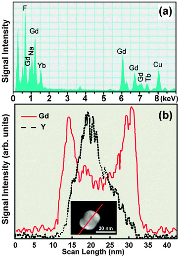 | ||
| Fig. 11 Composition characterization of UC nanocrystals by EDS. (a) EDS spectrum of NaGdF4:Yb/Tm (49/1 mol%)@NaGdF4:Tb (15 mol%) core–shell nanocrystals. (b) Elemental mapping of Gd3+ and Y3+ in a NaYF4@NaGdF4 core–shell nanocrystal with the direction along the line marked in inset. (Reprinted with permission from ref. 65 and 127. Inset shows the analyzed nanocrystal and the scanning line. Copyright 2011, Nature Publishing Group and American Chemical Society.) | ||
It has been challenging for EDS to quantitatively analyze the doping concentration of activators although its detection limit reaches 0.1 at% under optimized conditions (Table 2). For example, the detection of Tm3+ in NaYF4:Yb/Tm (20/0.2 mol%) nanocrystals by EDS is extremely difficult. Moreover, impurities (e.g., O and C) may easily interfere with the determination of the dopant ions. Additionally, samples containing many closely spaced X-ray lines from lanthanides, such as lanthanum and cerium, may also add a constraint to the quantitative mapping of the dopants.
5.2 EELS
By inspecting the energy loss of incident electron beam, EELS is another representative technique for qualitative and quantitative analysis of dopants in UC nanocrystals. The use of an angle-limiting aperture can limit the size of the volume element generating the energy-loss signal. As a result, the spatial resolution can be pushed down to 0.1–1 nm by the EELS technique, a resolution that is much higher than obtainable by EDS (approximately 1–10 nm) (Table 2). The differentiation of core–shell UC nanocrystals is easily achievable by the EELS analysis. For example, using such a high resolution technique Y3+ and Gd3+ elemental signals could be detected from the core and shell regions in a NaYF4@NaGdF4 nanocrystal (Fig. 12).134,162 Analogous to EDS, EELS in 1D or 2D scanning mode can also produce solid proof for the formation of core–shell UC nanocrystals.65,163 Moreover, the implementation of EELS analysis can reduce the amount of beam damage to UC nanocrystals because of its easy operation and fast characterization.127 By nature, the background signal of an EELS spectrum is stronger than that obtained by EDS analysis, attributable to inelastic scattering of atoms with the binding energy less than the edge energy. EELS spectra from thick samples (>50 nm) may be difficult to interpret due to plural scattering.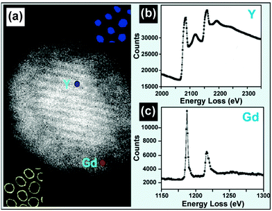 | ||
| Fig. 12 EELS technique for composition characterization of UC nanocrystals. (a) HADDF image of a single NaYF4:Yb/Er (20/2 mol%)@NaGdF4 core–shell nanocrystal. (b and c) EELS spectra of yttrium L2,3 and gadolinium M4,5 edges obtained from the NaYF4:Yb/Er (20/2 mol%) core and NaGdF4 shell as labeled in a. (Reprinted with permission from ref. 134. Copyright 2012, American Chemical Society.) | ||
5.3 XPS
A focused X-ray beam is also suitable as a light source to generate electrons for qualitatively or quantitatively probing surface composition of solid matters, a technique known as XPS. The amount of electrons and corresponding kinetic energies on X-ray irradiation is recorded by an electron energy analyzer for elemental analysis. Each element in a specific chemical environment has a characteristic binding energy (Ebinding) (eqn (5)).| Ebinding = Ephoton − (Ekinetc + ϕ) | (5) |
Owing to the weak escape capability of ejected electrons, XPS is only limited to characterize surface composition of UC nanocrystals with a thickness of less than 10 nm. The high sensitivity (down to ppm) of this technique, combined with the ability to measure the surface structure, makes this technique ideal for probing subtle variations on the surface of UC nanocrystals.64,124,171 For example, the replacement of Y3+ in NaYF4 by a trace amount of Gd3+ can be readily confirmed by XPS measurement but not other techniques, including XRD and EDS.38,165
Depth-dependent composition measurement by XPS provides an alternative method to study the dopant distribution in UC nanocrystals. By using synchrotron radiation, van Veggel and co-workers reported precise control over the penetration depth of X-rays in NaGdF4 nanoparticles.119,166,167 They found that the distribution of Y3+, Tb3+ or Nd3+ in the NaGdF4 nanoparticles is inhomogeneous. In a subsequent work, the researchers reported that the cation exchange competes with precipitation during the synthesis of core–shell nanocrystals. The resultant nanocrystals, as characterized by XPS, showed a concentration gradient of lanthanides or complex alloy structures.165 They further extended this approach to characterizing core–shell UC nanocrystals by analyzing the relative signal intensity of lanthanides as a function of the photoelectron kinetic energy.168 The gradually increased signal ratio of Y3+-to-Gd3+ along the penetration depth of a specimen revealed that the specimen is composed of NaGdF4@NaYF4 core–shell nanocrystals (Fig. 13).168 Unlike EDS and EELS techniques offering high spatial resolution, the spatial resolution of XPS is typically within the range of 5–30 μm (Table 2).
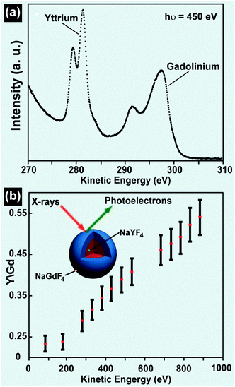 | ||
| Fig. 13 Composition characterization of UC nanocrystals by XPS technique. (a) Signals of yttrium 3d and gadolinium 4d core levels from NaGdF4@NaYF4 nanocrystals before the subtraction of the background (hν = ca. 450 eV). (b) Intensity ratio of yttrium (3d) to gadolinium (4d) core levels as a function of photoelectron kinetic energy. (Reprinted with permission from ref. 168. Copyright 2009, American Chemical Society.) | ||
5.4 ICP-MS and ICP-AES
The aforementioned three techniques are only applicable to micro-domain analysis within single or a small collection of nanocrystals. More reliable analysis that provides information on the average dopant concentration of lanthanides in UC nanocrystals is merely feasible by ICP-MS and ICP-AES measurements. Although the limit of detection for ICP-MS is about one order of magnitude higher than ICP-AES, both techniques can help identify the amount and type of elements present in lanthanide-doped UC nanocrystals.Both ICP-MS and ICP-AES techniques have been widely applied to probing the average concentrations of dopants in UC nanocrystals after chemical dissolution.16,19,25,29,122,125,162,169–173 It should be pointed out that the analytical results always deviate from the stoichiometric values used for the nanocrystal synthesis. In addition to the error caused by the imperfection of measuring instruments, different reactivity of lanthanide ions with ligands or with Na+ and F− may also contribute to the deviation. Using ICP-MS, Zhou et al. found that azelaic acid-capped NaGdF4:Yb/Er/Tm nanoparticles are first uptaken by liver and spleen, shortly after the injection of the particles (40 min), followed by heart, lung and kidney.174
Combined with laser ablation, the ICP-MS/AES analytical technique could be used for the bulk sampling of solid UC nanocrystals, in addition to being used for the analysis of solutions. An intrinsic limitation to ICP-MS is the possible spectroscopic interference by Re+ and ReO+ species formed during the step of ion generation. For ICP-AES measurement, the challenge lies in how to extract effective signals from background emissions.
6. Measurement of optical properties
Optical characteristics of lanthanide-doped UC nanocrystals are the most fascinating part of their properties. Anti-Stokes emissions of lanthanide activators have been achieved through effective energy transfer between sensitizers (Table 3) and activators (Table 4) or by excited state absorption of the activators.65,163 Unlike the vast majority of transition metal counterparts with only one emitting excited states, lanthanide dopants feature a series of f–f excited states, making them particularly suitable for use in UC materials. Due to the parity-forbidden 4f–4f transition, lanthanide-doped UC nanocrystals have long lifetimes of emission up to 20 ms and relatively small absorption cross-sections.130 For characterization of optical properties of UC nanocrystals, we start from the introduction of excitation source selection, including wavelength, power density and laser types (continuous-wave laser or pulse laser), then move to the measurement of emission, quantum yield and lifetime, followed by the discussion on the challenges in analyzing energy transfer efficiency between UC nanocrystals and other optical systems. A considerable effort is devoted to describing the integrated techniques for characterizing UC nanocrystals on the single-particle level. In the last part of this topic, we briefly summarize recent advances in instrumentation for in vitro and in vivo imaging.| Sensitizer | Absorption band (nm) | Excitation transition | Excitation wavelength (nm) | Ref. |
|---|---|---|---|---|
| Nd3+ | 860, 800, 740 | 4I9/2→4F3/2, 4F5/2/2H9/2, 4S3/2/4F7/2 | 808, 800, 795 | 163 and 175–178 |
| Yb3+ | 980 | 2F7/2→2F5/2 | 915, 980 | 149 and 179 |
| Er3+ | 1500, 970, 800 | 4I15/2→4I13/2, 4I11/2, 4I9/2 | 800, 980, 1490, 1530, 1560 | 180–182 |
| Ho3+ | 1140–1250 | 5I8→5I6 | 1160 | 182 |
| Activators | Emission peak locations (nm) | Energy transition | Ref. |
|---|---|---|---|
| Er3+ | 410, 523, 542, 660 | 2H9/2 → 4I15/2, 2H11/2 → 4I15/2, 4S3/2 → 4I15/2, 4F9/2 → 4I15/2 | 183 |
| Ho3+ | 542, 645, 658 | 5S2 → 5I8, 5F5 → 5I8 | 183 |
| Tm3+ | 294, 345, 368, 450, 475, 650, 700, 800 | 1I6 → 3H6, 1I6 → 3F4, 1D2 → 3H6, 1D2 → 3F4, 1G4 → 3H6, 1G4 → 3F4, 3F3 → 3H6, 3H4 → 3H6 | 183 |
| Tb3+ | 490, 540, 580, 615 | 5D4 → 7F6, 5D4 → 7F5, 5D4 → 7F4, 5D4 → 7F3 | 65, 184, 185 |
| Eu3+ | 590, 615, 690 | 5D0 → 7F1, 5D0 → 7F2, 5D0 → 7F4 | 65, 185, 186 |
| Sm3+ | 555, 590 | 4G5/2 → 6H5/2, 4G5/2 → 6H7/2 | 65, 185 |
| Dy3+ | 570 | 4F9/2 → 6H13/2 | 65, 185 |
| Ce3+ | 312, 331 | 4f5d → 2F5/2, 4f5d → 2F7/2 | 187 |
| Gd3+ | 311 | 6P7/2 → 8S7/2 | 65, 187 |
| Mn2+ | 585 | 4T1g(G) → 6A1g(S) | 188–190 |
6.1 Choosing appropriate excitation wavelength
A new direction of research in the field of UC is to broaden the range of wavelengths used for excitation. Previously, the excitation of 980 nm was oftentimes used because it perfectly matches the absorption band of Yb3+, typically doped in the UC nanocrystals as a sensitizer. In addition, the use of the Yb3+ sensitizer enables to achieve efficient energy transfer due to the effects of resonance – a process that occurs when the 2F7/2 → 2F5/2 transition of Yb3+ matches many f–f transitions of upconverting lanthanide ions (Er3+, Tm3+, and Ho3+). However, 980 nm laser sources for biological imaging often cause strong water absorption and sample overheating. To expand the excitation beyond the 980 nm laser, an effective solution is to use Nd3+ ions as the sensitizer for photon UC under 800 nm excitation, as Nd3+ features a sharp absorption band centered around 800 nm. Conversely, the excitation can be shifted to a wavelength much longer than 980 nm, as demonstrated by Prasad and co-workers in LiYF4:Er (10 mol%) colloidal solution.180 In their work, they observed an intense UC emission from the nanoparticle solution upon laser excitation at 1490 nm. In a parallel development, Wang and co-workers reported the fabrication of multilayer NaGdF4:Er@NaGdF4:Ho@NaGdF4 nanocrystals excitable by dual wavelengths, 1160 nm for Ho3+ and 1500 nm for Er3+.182 The strong UV-visible emissions of these nanocrystals upon NIR excitation potentially provide a much needed solution for reducing transmission loss in crystalline silicon solar cells.6.2 Excitation by continuous-wave (CW) laser
As photon UC is a representative non-linear optical process, the luminescence properties of UC nanocrystals are markedly dependent on the excitation source. In this section, we focus on the steady-state UC emissions of UC nanocrystals under excitation by CW lasers within different ranges of power density: 1–102 W cm−2 (low), 102–104 W cm−2 (medium) and 104–106 W cm−2 (high).| IUC ∝ InP | (6) |
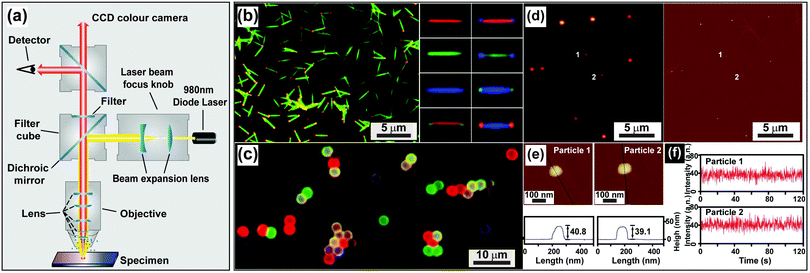 | ||
| Fig. 14 Characterization of UC nanocrystals under excitation at a medium power density. (a) Schematic configuration of a wide-field luminescence microscope. (b) Wide-field luminescence images of multicolored barcodes with an average length of 2 μm. (c) Wide-field luminescence image of UC nanocrystal-decorated polystyrene microspheres. (d) Luminescence image of NaGdF4:Yb/Er (20/2 mol%)@NaGdF4 core–shell nanocrystals and corresponding AFM characterization. (e) Size measurement of individual core–shell nanocrystals shown in (d). (f) The corresponding photophysical stability of the core–shell nanoparticles as shown in e on 980 nm excitation (100–170 W cm−2). (Reprinted with permission from ref. 65, 121 and 196. Copyright 2011, 2014 and 2009, Nature Publishing Group, American Chemical Society and Wiley-VCH Verlag GmbH & Co. KGaA.) | ||
UC nanocrystals or their aggregates with size larger than the diffraction limit of light (∼200 nm) can be clearly recognized by a wide-field optical microscope (Fig. 14b and c).65,121 Direct imaging of a single UC nanocrystal by a wide-field microscope is generally challenging but can be made possible with the assistance of other imaging techniques such as STEM or AFM. For example, Park and co-workers first demonstrated the measurement of UC luminescence of a single cubic-phase NaGdF4:Yb/Er@NaGdF4 nanoparticle by a two-step procedure.196 The first step is to localize the nanoparticle with precision via AFM, and the following step involves spectroscopic study of the nanoparticle using a wide-field fluorescence microscope (Fig. 14d–f). The authors provided concrete evidence that lanthanide-doped nanocrystals have exceptionally high photostability against laser beam illumination (100–170 W cm−2) for 4 h. In a recent work by the same group, they suggested that the high photostability against photobleaching is a general characteristic of the UC nanocrystals, regardless of whether different host materials or core–shell strategies are implemented.197
 | ||
| Fig. 15 Characterization of UC nanocrystals under excitation at a high power density. (a) Confocal UC luminescence imaging of UC nanocrystals on a silicon nitride membrane (inset: corresponding SEM image in transmission mode). (b) Time-dependent emission intensity of a single UC nanocrystal under continuous laser illumination with a power density of about 3 × 10⁶ W cm−2. (c) Zoom-in time trace and histogram of emission intensity of a UC nanocrystal showing a non-blinking characteristic. (d) Luminescence intensity of a single nanocrystal comprising NaYF4:Yb/Er (20/20 mol%, blue circles) and NaYF4:Yb/Er (20/2 mol%, red circles), respectively, plotted as a function of excitation intensity. Note that the inset shows zoom-in of the luminescence intensity cross-over region measured for the two different nanocrystals. (e–g) Confocal luminescence images taken at points shown in (d). The images were collected at increasing excitation intensity. Dashed lines indicate the region from which luminescence intensity was collected for d. The scale bar in (e–g) is 1 μm. (Reprinted with permission from ref. 198 and 201. Copyright 2009 and 2014, National Academy of Sciences, USA and Nature Publishing Group.) | ||
Polarized energy transfer UC in a single hexagonal NaYF4:Yb/Tm (18/2 mol%) microrod was recently demonstrated by Zhou et al., who exploited confocal microscope imaging coupled with a linearly polarized laser. The authors argued that the polarization anisotropy, induced by intra-ionic transition and the breaking of crystal local site symmetry, is responsible for the polarized UC emissions.199 By using excitation with intense power density (up to 2.5 × 10⁶ W cm−2), Jin and co-workers observed a suppressed concentration-quenching effect in UC nanocrystals containing a high concentration of Tm3+ (8 mol%).200
Similar results were observed by Gargas et al. from ultrasmall NaYF4 nanoparticles (5 nm) co-doped with Yb3+/Er3+ (20/20 mol%).201 The authors found that the brightness of these nanoparticles can surpass the conventional nanoparticles (β-NaYF4 with 20% Yb3+ and 2% Er3+) when the power density reaches ∼3.0 × 10⁵ W cm−2 (Fig. 15d–g). Such ultra-small, bright UC nanocrystals may find use in a range of applications, particularly in the area of single-molecule detection. An additional benefit of high power density excitation lies in its ability to trap single UC nanocrystals and perform in situ optical characterization.202
6.3 Pulse-laser excitation
In contrast to extensive studies of steady-state excitation, less attention is paid to investigations on UC nanocrystals under excitation of pulse laser with the exception of lifetime measurements. The advantages of pulse laser excitation derive from variations in pulse in terms of repetition rate, peak power and pulse width. Owing to the power density-dependent emission of UC nanocrystals, pulse laser excitation, in principle, provides a valuable handle for spectroscopic studies.Upon excitation with pulse-widths in the order of microsecond or millisecond comparable to the lifetimes of the intermediate states of lanthanide activators, a significant increase in quantum yield of UC nanocrystals is achievable as a result of a high fluence rate. For example, Liu and co-workers reported that an optimal signal gain (ratio of the quantum yieldpulsed/quantum yieldCW) up to 8.7 was obtained from NaYF4:Yb/Tm (25/0.3 mol%)@NaYF4 core–shell nanocrystals under 2 Hz square-wave pulse excitation (power density: 0.12 W cm−2; pulse width: 20 ms) (Fig. 16).203 The quantum yield of NaYF4:Yb/Tm nanocrystals doubled under excitation of a 5 KHz square-wave pulse (peak power: 1 W; pulse width: 200 μs).204 It is worth mentioning that the combination of high brightness of each pulse with discrete excitation facilitates realization of single-shot deep tissue imaging without autofluorescence and concerns of the overheating effect.
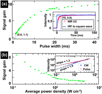 | ||
| Fig. 16 Study of photon UC of lanthanide-doped nanocrystals under excitation of a millisecond single pulse. (a) The NIR UC signal gain of NaYF4:Yb/Tm (25/0.3 mol%)@NaYF4 core–shell nanocrystals upon pulse excitation with different pulse widths (IRF-the instrument response function). (b) The dependence of NIR UC signal gain on the average power density under excitation of pulse-laser (pulse width, 20 ms; repetition rate, 2 Hz). Insets: the response of the NIR UC emission to a square-wave excitation (inset a) and the average power density dependences of the NIR UC emission intensity under CW and pulsed excitations (inset b), respectively. (Reprinted with permission from ref. 203. Copyright 2013, Royal Society of Chemistry.) | ||
When the pulse width is reduced to nanoseconds which is much shorter than the lifetime of the intermediate states of lanthanide activators, it has a negligible impact on the quantum yield of the UC nanocrystals. However, for short pulse widths with high power density (108 to 109 W cm−2), it is applicable to excite the nanocrystals for achieving multi-photon UC emission. Moreover, the high power density of the pulse can lead to a large population inversion for optical lasing by sequential pulse excitation of UC nanocrystal colloids using an optical parametric oscillator laser.205
6.4 Emission characterization
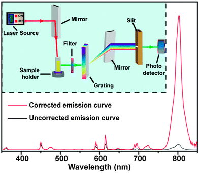
Commercially available or customized luminescence spectrophotometers, coupled with an external laser source, are regarded as workhorse instruments for studying luminescent properties of UC nanocrystals (Fig. 17). A spectrophotometer section generally contains a filter, grating mirrors and a photon detector. At present, most of the photon detectors comprise a photomultiplier (PMT) for converting impinging photons into electronic charges and an optimized dynode chain for the amplification of secondary electrons. The emission spectrum of UC nanocrystals encompasses a wide range of wavelengths from UV to NIR spectral regions, thus imposing a critical requirement for PMT to effectively convert all emitting photons to electrons. The sensitivity of PMT to emissions at different wavelengths varies significantly and strongly depends on the composition of photocathodes. For example, GaAsP and GaAs photocathodes are only sensitive to the photons in the ranges of 250–650 nm and 300–800 nm, respectively. The wavelength-dependent sensitivity of PMT indicates that detector correction is necessary, especially for customized spectrophotometers prior to emission characterization. For example, a striking difference in the emission ratio of NIR-to-visible was observed from the corrected and uncorrected emission spectra of NaGdF4:Yb/Tm (49/1 mol%)@NaGdF4:Eu (15 mol%) core–shell nanocrystals (Fig. 17). The correction for emission ratio differences can be quite important when measuring quantum yields or collecting data in order to form the CIE chromaticity diagram. Moreover, owing to the multi-band emission feature of UC nanocrystals, filters in some cases are needed to prevent the generation of overtone bands. For emission measurements, a quartz vial is preferred over glass or plastic vials because they have different levels of absorption in the UV, visible or NIR region.The choice of the host lattice and the level of impurity concentration have strong effects on the emission of UC nanocrystals measured at different temperatures. Pires et al. reported on the suppression in the emission intensity of Y2O3:Yb/Er UC nanocrystals with increasing temperature from 10 to 300 K, indicating the enhancement of non-radiative multiphonon relaxation at elevated temperatures.206 Yu et al. studied the effect of the crystal phase on the emission of NaYF4:Yb/Er nanocrystals.207 The authors found that the emission intensity of cubic phase nanocrystals decreased monotonically as the temperature was increased from 10 to 400 K, while hexagonal phase counterparts exhibited maximum emission intensity at 100–150 K under identical experimental conditions. They ascribed this result to the competition between two optical processes: energy transfer from 2F5/2|1〉 of Yb3+ to 4I11/2|0〉 of Er3+ and concurrent promotion of non-radiative relaxation at elevated temperatures.208 It is interesting to note that the intensity ratio of two emissions arising from 2H11/2 → 4I15/2 (at 523 nm) and 4S3/2 → 4I15/2 (at 542 nm) transitions of Er3+ is highly sensitive to temperature under low power density excitation. This effect can be harnessed to develop thermal sensors for use in the measurement of deep tissue temperature.209
Low-temperature luminescence spectroscopy brings a new dimension to systematic investigations of energy transfer mechanism between the lanthanides doped in UC nanocrystals. For example, Suyver and co-workers observed that the emission intensity of NaYF4:Yb/Er (18/2 mol%) nanoparticles measured at an ultralow temperature of 5 K is several orders of magnitude lower than that obtained at room temperature.10 Much of the observed phenomenon was associated with the absence of direct energy transfer from Yb3+ to Er3+ caused by the low temperature factor. High resolution optical measurements of UC nanocrystals at low temperature are also useful in interpreting the site symmetry of activators. On the basis of the UC luminescence spectrum obtained at 10 K for Y2O3:Yb/Er (1/2 mol%) nanocrystals, Güdel and co-workers predicted different site symmetries (C2 and C3i) of Y3+ upon substitution by Er3+ in the host lattice.206
6.5 Absolute quantum yield measurement
Absolute quantum yield (Φ) of UC nanocrystals is the direct measure of the efficiency of the conversion of NIR incident photons into visible or even UV emission. It is defined as the ratio of the number of UC photons emitted (Nemission) to the number of photons absorbed (Nabsorption) (eqn (7)). | (7) |
The measurement of the absolute quantum yield of UC nanocrystals relies on two indispensable components: an integrating sphere by which the emission from nanocrystals are scattered and an extended spectrometer for analyzing the scattered photons (Fig. 18).210 In 1998, Page et al. measured the UC quantum yield of NaYF4:Yb/Er (18/2 mol%) and NaYF4:Yb/Tm (27/0.1 mol%) in bulk form through use of the integrating sphere.211 In 2010, van Veggel's group took one step forward and first measured the absolute quantum yield of NaYF4:Yb/Er (20/2 mol%) nanocrystal colloids.212 Absolute quantum yields in the range of 0.005% to 0.3% were measured for several batches of nanoparticles with particle sizes of 10 to 100 nm, while a quantum yield of 3% was obtained for a bulk control. This method has been widely utilized to determine the quantum yields of different types of UC nanocrystal colloids (Table 5). Critically, the quantum yield of UC nanocrystals without the core–shell structure is generally low ranging from 0.0022 to 1.2%.78,116,180,210,212–214 By comparison, the shell-passivated UC nanocrystals showed largely improved conversion efficiencies (0.18–7.6%).180,210,212–215 Obviously, the quantum yields of nanosized UC particles is much lower than the expected theoretical value (100/n%) resulting from an n-photon-UC process. The low efficiency observed for UC nanocrystals is likely due to non-radiative cross-relaxation between lanthanide dopants, in addition to down-shifting emissions by sensitizers (e.g., 1030 and 1050 nm of Yb3+) and activators (e.g., 1530 nm of Er3+).
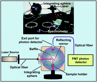 | ||
| Fig. 18 Schematic illustration and photograph (inset) of a typical instrument setup for the quantum yield measurement of UC nanocrystal colloids. Note that the setup typically comprises an integrating sphere, an external excitation source and a photomultiplier photon detector. (Reprinted with permission from ref. 210. Copyright 2012, American Chemical Society.) | ||
| Composition (mol%) | Phase | Size (nm) | Power density (W cm−2) | Φ (%) | Ref. | |
|---|---|---|---|---|---|---|
| a ex = 1490 nm. | ||||||
| Bulk | NaYF4:Yb/Er (20/2) | Hexagonal | — | 20 | 3.0 ± 0.3 | 212 |
| Core nanoparticle | NaYF4:Yb/Er (20/2) | Hexagonal | 100 | 150 | 0.30 ± 0.10 | 212 |
| NaYF4:Yb/Er (20/2) | Hexagonal | 30 | 150 | 0.10 ± 0.05 | 212 | |
| NaYF4:Yb/Er (20/2) | Hexagonal | 8–10 | 150 | 0.005 ± 0.005 | 212 | |
| NaYF4:Yb/Er (20/2) | Hexagonal | 5.4 | 1000 | 0.0022 ± 0.0001 | 78 | |
| NaYF4:Yb/Er (20/2) | Hexagonal | 37 | 1000 | 0.14 ± 0.01 | 78 | |
| NaGdF4:Yb/Er (20/2) | Hexagonal | 5 | 100 | 0.016 ± 0.008 | 210 | |
| LiYF4:Er (10) | Tetragonal | 85 | 150a | 1.2 ± 0.1 | 180 | |
| LiLuF4:Yb/Er (20/1) | Tetragonal | 28 | 127 | 0.11 | 213 | |
| LiLuF4:Yb/Tm (20/0.5) | Tetragonal | 28 | 127 | 0.61 | 213 | |
| NaYF4:Yb/Tm (25/0.3) | Hexagonal | 38 | 3.8 | 0.45 | 214 | |
| NaLuF4:Gd/Yb/Tm (24/20/1) | Hexagonal | 7.8 | 17.5 | 0.47 ± 0.06 | 116 | |
| Core–shell Nanocrystal | NaYF4:Yb/Er (20/2)@NaYF4 | Hexagonal | 30 | 150 | 0.30 ± 0.10 | 212 |
| NaYF4:Yb/Er (20/2)@NaYF4 | Hexagonal | 9 | 1000 | 0.18 ± 0.01 | 180 | |
| NaGdF4:Yb/Er (20/2)@NaYF4 | Hexagonal | 17 | 100 | 0.51 ± 0.01 | 210 | |
| NaYF4:Yb/Tm (25/0.3)@NaYF4 | Hexagonal | 42 | 78 | 3.5 | 215 | |
| NaYF4:Yb/Tm (25/0.3)@NaYF4 | Hexagonal | 43 | 1.3 | 1.2 | 214 | |
| LiLuF4:Yb/Er (20/1)@LiLuF4 | Tetragonal | 40 | 127 | 3.6 | 213 | |
| LiLuF4:Yb/Er (20/1)@LiLuF4 | Tetragonal | 50 | 127 | 5.0 | 213 | |
| LiLuF4:Yb/Tm (20/0.5)@LiLuF4 | Tetragonal | 40 | 127 | 6.7 | 213 | |
| LiLuF4:Yb/Tm (20/0.5)@LiLuF4 | Tetragonal | 50 | 127 | 7.6 | 213 | |
Of particular note is our inability to quantitatively compare different quantum yields reported thus far for UC nanocrystals. This is because absolute UC quantum yields depend highly on experimental conditions, especially the power density of the excitation source.211 Additionally, different brands of photon detectors may lead to considerable deviation as well. To ensure the validity of quantum yield characterization, careful correction of the photon detector must be performed prior to the spectroscopic measurement.
6.6 Lifetime measurements
The combination of a spectrophotometer and a pulse laser is a standard instrument for investigating emission dynamics of UC nanocrystals. For example, the temporal emission evolution of the UC nanocrystals is usually recorded on a commercially available phosphorescence lifetime spectrometer coupled with a tunable mid-band optical parametric oscillator pulse laser.As illustrated in Fig. 19a and b, two types of time-resolved spectral evolution curves representing different UC mechanisms216 are commonly collected after pulse excitation: (i) single exponential decay accounting for an excited state absorption (ESA) UC process and (ii) short rise time followed by a relatively slow exponential decay, characteristic of an energy transfer UC process. The rising time in the energy transfer UC process is strongly correlated to the structure of the UC nanocrystals under investigation. For example, multilayer NaYF4:Yb/Tm (30/0.5 mol%)@NaYbF4@NaYF4 nanocrystals require a much longer time (2.5 ms) to populate the 3H4 state of Tm3+ than other types of core–shell structured UC nanocrystals, such as NaYF4:Yb/Tm (30/0.5 mol%)@NaYbF4 (1 ms) and NaYF4:Yb/Tm (30/0.5 mol%)@NaYF4 (1.3 ms).217
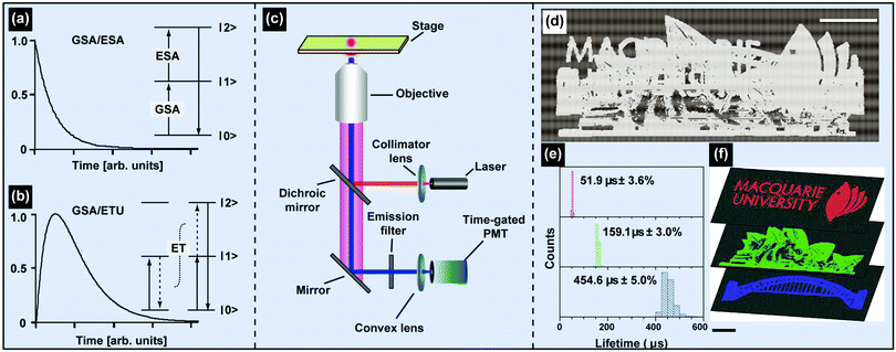 | ||
| Fig. 19 Luminescence lifetime characterizations of UC nanocrystals and demonstration of their use for security printing application. (a and b) Typical time evolution of UC emission after short-pulse excitation and their correlation with different photon UC mechanisms (GSA: ground state absorption, ESA: excited state absorption, ETU: energy transfer upconversion). (c) Schematic of a representative setup for studying time-resolved UC emission. (d) Demonstration of UC nanocrystals for use as security ink. (e) Graphs showing different lifetimes of the nanocrystals generated by controlling the concentration ratio of Yb3+ and Tm3+. (f) Demonstration of optical information storage using lifetime-encoded UC nanocrystals. Three overlaid patterns, printed with nanocrystals of three different lifetimes, can be decoded and separately read out by a time-resolved confocal fluorescence microscope equipped with a 980 nm laser. Note that the emission color is the same in all cases; the red, green and blue colors in the figure indicate the different lifetimes (scale bar: 5 μm). (Reprinted with permission from ref. 216 and 220. Copyright 2005 and 2014, Elsevier Ltd and Nature Publishing Group.) | ||
The lifetime of UC nanocrystals can be drawn from the decay curve by means of different approaches. If the decay curve fits eqn (8), the lifetime is then obtained directly from the fitting. Otherwise, the effective lifetime would be used and calculated according to eqn (9).
 | (8) |
 | (9) |
The lifetime of UC nanocrystals has a profound relationship with their parameters such as the size, phase, doping concentration and core–shell structure. Recently, Jin and co-workers demonstrated that the lifetime of NaYF4:Yb/Er (18/2 mol%) nanoparticles reduces gradually with decreasing particle size from 45 to 6 nm. The authors ascribed this effect to the increased density of crystalline defects as the size of the nanoparticles reaches several nanometers.218 An interesting finding is that the lifetime of red emission (4F9/2 → 4I15/2, Er3+) is always much longer than that of green emission (4S3/2 → 4I15/2, Er3+).194
An inert-shell coating provides the particles with optical protection against perturbation by surrounding environments, thereby allowing the lifetime of activators to be extended as demonstrated by Zhang and co-workers in NaYF4:Yb/Er (20/2 mol%)@NaGdF4 core–shell nanocrystals.134 They found that the lifetime of Er3+ at the 4S3/2 state is accumulated from 287 to 762 μs as the shell thickness increases from a monolayer of single atoms to six monolayers. Li and co-workers investigated NaGdF4:Er (3 mol%)@NaYF4 core-mesoporous shell nanocrystals and successfully identified the location of emissive Er3+ in the center of the core or at the core–shell interface by time-resolved spectroscopic studies.219
Inter-ionic energy transfer is a dominating factor concerning variations in the lifetime of an emissive intermediate state of lanthanides doped in UC nanocrystals. For example, the lifetime of Gd3+ emission at 310 nm (6P7/2 → 8S7/2) of NaGdF4:Yb/Tm (49/1 mol%)@NaGdF4 core–shell nanoparticles decreased significantly from 1011 to 555 μm when Tb3+ (15 mol%) ions were incorporated into the shell layer in favor of energy transfer from Gd3+ to Tb3+.65,185 Similarly, the lifetime of Tm3+ emission at 475 nm (1G4 → 3H6) of NaYF4:Yb/Tm nanocrystals could be tuned from 25.6 to 662.4 μs through control over energy transfer between Yb3+ and Tm3+ ions by varying the molar ratio of Yb3+-to-Tm3+ from 20/8 to 20/0.2.220
UC nanocrystals with tunable lifetimes hold great promise in multiplexing and document coding.221 Emissions with different lifetimes can be spectroscopically resolved or microscopically imaged with the help of a time-gated PMT. For example, Chen and co-workers demonstrated that it is possible to separate long-lived red emission of Eu3+ and short-lived blue emission of Tm3+ from NaGdF4:Yb/Tm (18/1 mol%)@NaGdF4:Eu (10 mol%) core–shell nanocrystals by the time-resolved luminescence technique.222 In another impressive work demonstrated by Jin and co-workers, different patterns encoded with UC nanocrystals of varied lifetimes could be interpreted in a layer-by-layer fashion through use of a time-gated microscope (Fig. 19c–f).220 One limitation associated with such security printing application is purely technical: no known robust methods are currently available for the synthesis of lifetime-tunable UC nanocrystals displaying similar brightness.
It is worthy of note that the lifetimes of UC nanocrystals reported previously are irrespective of the excitation power density up to 500 W cm−2.223 However, a recent study has confirmed that upon excitation with a high power density (e.g., 106 W cm−2), the lifetimes of the intermediate states responsible for visible emission photons would be shortened as a result of elevated energy transfer rates and cross-relaxation processes.201
6.7 Energy transfer measurement
The characterization of energy transfer between UC nanocrystals and other suitable energy acceptors or occasionally energy donors, including organic dyes, quantum dots and semiconducting thin films is of fundamental importance to designing high-sensitivity biosensors and improving NIR light harvesting of photovoltaic cells.27,224 Non-radiative energy transfer (Dexter exchange or the Förster resonance mechanism) and radiative energy transfer are the two major pathways that govern the energy transfer of UC nanoparticle-involved systems.229,230 The efficiency of energy transfer (E) between the energy donor and acceptor can be quantified by the fraction of an energy transfer event occurring per donor excitation event (eqn (10) or (11)): | (10) |
 | (11) |
Sharp emission bands of lanthanide activators make UC nanocrystals suitable as excellent energy donors, allowing one to construct energy transfer systems involving a wide range of energy acceptors, including plasmonic nanocrystals, organic dyes, quantum dots and metal oxides.120,225–227 In such systems, the efficiency of energy transfer is within the range of 10–90%, depending on the relative molar ratio between the energy donor and energy acceptor. For example, Wang et al. reported that the green emission of NaYF4:Yb/Er (4/2 mol%) nanocrystals at 543 nm could be effectively transferred to gold nanoparticles with a high efficiency up to 70%.227 To optimize the energy transfer efficiency, an inert-shell with critical thickness of several nanometers is essential for preserving energy of excited donors, while inducing negligible separation between the energy donor and acceptor.67
Non-radiative energy transfer at a short range typically renders a higher efficiency relative to the energy transfer via a radiative pathway. As a result, it is deemed that the radiative energy transfer plays a trivial role in the energy transfer process.61,67,228,229 For example, Riuttamäki and colleagues confirmed a non-radiative energy transfer from UC nanocrystals to fluorescent dyes in aqueous suspensions, as evident by a decreased lifetime of UC nanocrystals, without concerning radiative energy transfer.230
To achieve broadband excitable UC nanocrystals, recent studies have shifted the focus of research on developing UC nanocrystals for use as energy acceptors. For example, a relatively efficient energy transfer (E = ∼50%) from organic dyes to NaYF4:Yb/Er (20/2 mol%) nanoparticles was observed, generating a new class of UC nanomaterials excitable by a broadband from 740 to 850 nm.231 Despite the success, two concerns were presented in their study: (i) low UC efficiency of the dye-sensitized UC nanocrystals due to back-energy transfer to the dye molecules and down-shifting emission of the activators and (ii) low photostability of the hybrid system arising from the photobleaching effect of the dye molecules. The second concern was confirmed by Hyppänen et al., who illustrated that almost 50% of IR-806 dye molecules were bleached after 30 s of laser beam irradiation (power density: 9.5 W cm−2).232
A Förster resonance energy transfer model, suitable for the situation between molecular donors and acceptors, has been utilized to study the efficiency of energy transfer between UC nanocrystals and suitable energy acceptors in close proximity (eqn (12)).
 | (12) |
Energy transfer between different lanthanide activators, doped in two neighboring segments of a microstructure, can be probed by measuring the lifetime of the activators. For example, Zhang et al. reported the synthesis of a dual-color emitting microrod by incorporating Tm3+ and Er3+ activators into the central segment and two tips of the microrod, respectively (Fig. 20).121 Using a confocal microscope equipped with a lifetime spectrometer, the researchers found that the green (4S3/2 → 4I15/2) and red (4F9/2 → 4I15/2) emission lifetimes of Er3+ measured from different parts of the microrod are essentially the same, implying that no obvious interfacial crosstalk between Tm3+ and Er3+ occurs. Critically, this technique has limitations for measuring energy transfer between microdomains within a microsized particle because of relatively large size in the focal spot (400 nm in radius) of the confocal microscope. Combined with the recently emerged stimulated emission depletion (STED) method, this approach may enable us to precisely map emission profiles within a single UC nanocrystal because of the high resolution capability of STED (∼2.4 nm).234
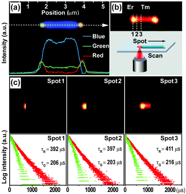 | ||
| Fig. 20 Characterization of energy transfer within an UC microrod. (a) Wide-field luminescence image of the microrod exhibiting YBY dual-color upconversion emission. Note that the color component of the emission can be resolved by RGB acquisition. (b) Confocal microscope image showing a different dual-color microrod. (c) Corresponding green (4S3/2 → 4I15/2) and red (4F9/2 → 4I15/2) emission lifetimes in three different areas (marked with spot 1, 2, 3 shown in (b) of the microrod. Note that spot 1 contains only Er3+. Spot 2 contains Er3+ and a small amount of Tm3+. Spot 3 is codoped with Er3+ and a large amount of Tm3+. (Reprinted with permission from ref. 121. Copyright 2014, American Chemical Society.) | ||
6.8 AFM-coupled spectrometer for single particle imaging
An AFM-coupled spectrophotometer is an integrated instrumental setup capable of measuring the size, morphology, and optical properties of single UC nanocrystals simultaneously (Fig. 21a).235 The combination of AFM with optical spectroscopy can largely simplify the characterization process for single UC nanocrystals as compared to conventional light microscopes.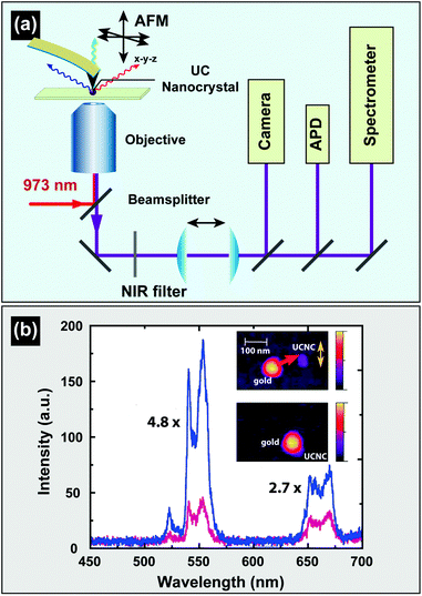 | ||
| Fig. 21 Characterization of UC nanocrystals on the single-particle level through use of an AFM-coupled spectrophotometer. (a) Schematic illustration of the instrument setup. (b) Luminescence emission spectra of a single UC nanocrystal measured in the presence (blue curve) and absence (violet curve) of a gold nanoparticle (see the inserted panels) in close proximity. Note that the green and red emissions of the nanocrystal are enhanced by a factor of 4.8 and 2.7, respectively. (Reprinted with permission from ref. 236 and 239. Copyright 2009, American Chemical Society.) | ||
With the help of AFM, Schietinger and colleagues reported an abnormal size-dependence of the UC emission, on the single-particle level, for NaYF4:Yb/Er nanocrystals.236–238 In their report, the authors found that the emission intensity ratio of green-to-red measured from single nanocrystals can be quite different, depending on their size. They attributed this aberration to different degrees of phonon confinement in nanocrystals of dissimilar sizes. The authors further utilized their instrument setup to elucidate plasmonic effects on UC emission by in situ monitoring the variations in the emission intensity of a UC nanoparticle in response to changes in the distance between the UC nanoparticle and a gold nanoparticles, placed in close proximity (Fig. 21b).239In situ optical characterization revealed that apart from an enhancement in the UC emission of the nanoparticle with an overall factor of 3.8, the nanoparticle showed increased excitation and emission rates when placed in the vicinity of a metal nanoparticle. The AFM-coupled spectrophotometer may also find useful application for correlating the effect of different parameters of a plasmonic nanorod, such as size, morphology and exciton-coupling orientation (e.g., side-by-side or end-to-end) on the emission of an UC nanocrystal.240
6.9 In vitro and in vivo imaging measurement
With UC nanocrystals designed as luminescent biomarkers to target cells and tissues, optical microscopes can be exploited for investigating cellular and tissue functions in situ or in vitro.241–243 For example, a conventional wide-field fluorescence microscope coupled with a CCD camera was applied to acquire high quality cell images in the presence of UC nanocrystals, benefitting from the absence of autofluorescence.178,244,245 To further improve subtle depth discrimination and achieve 3D visualization of the specimen under investigation, confocal microscopy can be furnished by virtue of its point-by-point scanning capability, equipped with a pinhole aperture to block the signals generated by the sample outside of the optical focus. By modifying a common inverted microscope, Li and co-workers constructed a laser scanning confocal UC luminescence microscope having a spatial resolution comparable to that of a conventional confocal microscope (Fig. 22a).246 As the imaging is based on the detection of anti-Stokes luminescence from UC nanocrystals, a short-pass excitation dichroic mirror is required to separate the emission from NIR excitation. Many other groups also demonstrated the benefit of using the scanning confocal UC luminescence imaging for high-resolution cell imaging and particle trafficking within the cells.35,116,158,198,247–251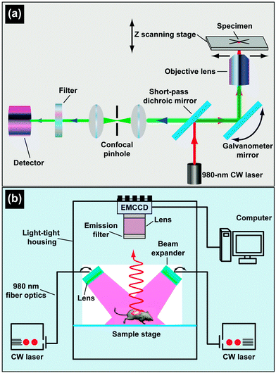 | ||
| Fig. 22 Schematic setup used for in vitro and in vivo imaging of cells and animals. (a) Schematic illustration of a laser scanning UC luminescence confocal microscope for in vitro study. (b) Experimental setup for in vivo imaging of small animals using UC nanocrystals as biomarkers. (Reprinted with permission from ref. 173 and 246. Copyright 2009, American Chemical Society.) | ||
For small animal non-invasive imaging involving UC nanocrystals, a variety of imaging modalities can be developed, including tumor-targeted imaging, lymphatic imaging, vascular imaging, and cell tracking. For example, a representative in vivo imaging system was constructed by combining a 980 nm laser with a high quality CCD camera and a filter to eliminate scattered NIR light.85,242,252 Note that commercially available in vivo imaging systems for small animals are difficult to apply to UC luminescence imaging because high-quality short-pass filters are required to attenuate the strong interference from the excitation source.20,173,243 A more detailed discussion of the customized instrumental setup for small animal imaging was presented by Xiong et al. (Fig. 22b).173 In a typical imaging experiment, two external adjustable CW 980 nm lasers were adopted as an excitation source, and an Andor DU897 EMCCD was utilized as a signal collector. A filter was placed in the front of the collector to block the scattered excitation photons. Taking advantage of this setup, short-term (24 h) and long term (115 days) in situ tracking of the distribution of NaYF4:Yb/Er/Tm nanocrystals in mice were conducted (Fig. 23).19,173 The results showed that a large portion of the nanocrystals was first accumulated in the liver and spleen, and further excreted from the body by hepatobiliary transport. Notably, the results on the retention time from long tracking (up to 90 days in intestinal tract) is slightly different from those obtained from ICP-AES measurement (7 days) reported by Zhang's group.125 Through use of β-NaLuF4:Gd/Yb/Tm nanoparticles, Li and co-workers achieved a detection limit of less than 50 cells for whole-body luminescence imaging of a small mouse with a penetration depth of ∼2 cm.116 A major challenge of this in vivo UC imaging approach is the development of the high throughput systems to evaluate a large number of small animals for screening purposes.
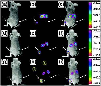 | ||
| Fig. 23 Time-dependent in vivo UC luminescence imaging of subcutaneous U87MG tumor (left hind leg, indicated by short arrows) and MCF-7 tumor (right hind leg, indicated by long arrows) borne by athymic nude mice after intravenous injection of RGD-coupled UC nanocrystals over a period of 24 h. (a–c) 1 h. (d–f) 4h. (g–i) 24 h. Note that columns 1, 2 and 3 are respective bright-field image, UC luminescence image and overlay of luminescence and bright-field images. (Reprinted with permission from ref. 173. Copyright 2009, American Chemical Society.) | ||
7. Evaluation of magnetic properties
Lanthanide-doped UC nanocrystals not only have excellent optical characteristics but also possess attractive magnetic properties which may hold promise as bioprobes for multimodal imaging.174,196,253 The magnetic properties of UC nanocrystals mainly derive from lanthanide ions with unpaired inner 4f electrons, such as Gd3+, Nd3+, Dy3+ and Ho3+. Owing to the shielding effect of 5s- and 5p-electrons, these ions have localized, noninteracting magnet moments, giving rise to paramagnetism.254The magnetic properties of the nanocrystals are normally investigated by a commercially available SQUID magnetometer or VSM. The paramagnetic behavior observed at room temperature for GdF3 and NaGdF4 nanocrystals is drastically different from that of Gd metal (ferromagnetism) due to poor overlapping of 4f orbitals of neighboring Gd3+ ions in host materials (Fig. 24).255,256 The magnetization and magnetic mass susceptibility of UC nanocrystals are sensitive to the content of magnetic lanthanide ions in host matrices. For instance, the magnetic mass susceptibility of pure NaGdF4 nanocrystals (16 nm) was changed from 9.29 × 10⁻⁵ to 7.46 × 10⁻⁵ emu gOe−1 after co-doping of Yb3+/Er3+ (20/0.2 mol%).257 Alternatively, the magnetic properties of the nanocrystals can be manipulated by introducing non-magnetic lanthanide ions such as Y3+.256,258 Size-dependent magnetic properties of lanthanide-doped nanocrystal were observed in NaYF4:Yb/Gd/Tm (30/40/2 mol%) nanorods and attributed to “spin-canting effects”, by which the tilted spins located near the surface of the nanocrystal result in a weak magnetization.253 Despite their relative weak magnetic force (1.05–1.85 emu g−1, 20 kOe) at room temperature, UC nanocrystals should find useful applications for bio-separation as they are recoverable through use of an external magnet (inset of Fig. 24).169,180,256,258–261
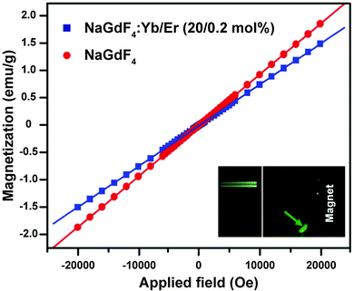 | ||
| Fig. 24 Magnetization of NaGdF4:Yb/Er (20/0.2 mol%) and NaGdF4 nanocrystals as a function of the applied field. Note that inset shows luminescent photographs of NaGdF4:Yb/Er nanocrystals, recorded under excitation at 980 nm, with and without a magnet, indicating that these UC nanocrystals can be recovered by applying an external magnetic force. (Reprinted with permission from ref. 256. Copyright 2011, American Chemical Society.) | ||
The evaluation of UC nanocrystals as magnetic contrast agents was conducted using commercially available instruments, for example 3T Siemens Magnetom Trio.174 Gadolinium-containing nanocrystals such as GdF3, NaGdF4, Gd3+-doped and NaGdF4 core–shell nanocrystals were extensively investigated to test their suitability as positive contrast agents for shortening longitudinal (T1) relaxation time of water protons (Table 6).130 Such studies revealed that small-sized NaGdF4 or GdF3 nanoparticles with a high doping content of Gd3+ are preferred in order to achieve a better T1 enhancement because of its concentration dependence of Gd3+ ions in close proximity to water molecules. Alternatively, a thin NaGdF4 shell coating of lanthanide-doped UC nanoparticles can render the nanoparticles with both improved T1 performance and enhanced UC emission. By comparison, Dy3+-containing nanocrystals are more suitable as negative contrast agents for shortening the transverse (T2) relaxation time of water protons.169 A mass effect on T2 relaxation has been reported by van Veggel's group using NaDyF4 UC nanoparticles.169 Their study suggested the use of large-sized Dy3+-based nanocrystals to enable high spatial and temporal resolution for T2 performance.
| Type of CAs | Composition (mol%) | Size (nm) | Magnetic field strength (T) | Molar relaxivity (mM−1 s−1) | Ref. | ||
|---|---|---|---|---|---|---|---|
| r 1 | r 2 | ||||||
| a The diameter of the UC nanocrystal component in the heterostructures. | |||||||
| Positive CAs (T1) | NaGdF4 core | NaGdF4 | 2.5 | 1.5 | 7.2 | — | 262 |
| NaGdF4:Yb/Er (18/2) | 10 | 4.7 | 0.99 | — | 263 | ||
| NaGdF4:Yb/Er (18/2) | 40 | 4.7 | 0.47 | — | 263 | ||
| NaGdF4:Yb/Er (20/2) | 20 | 1.5 | 1.40 | — | 196 | ||
| NaGdF4:Yb/Er (18/2) | 14 | 3 | 3.3 | — | 264 | ||
| NaGdF4:Yb/Er/Tm (20/1.8/0.2) | 25–60 | 3 | 5.6 | — | 174 | ||
| NaGdF4:Y/Yb/Er (39/10/1) | 80–100 | 3 | 2.273 | — | 265 | ||
| NaGdF4:Y/Yb/Er (20/18/2) | 19 × 22 | 3.0 | 0.405 | — | 266 | ||
| Gd2O3:Yb/Er (18/2) | 2.5 × 18 | 9.4 | 1.5 | — | 267 | ||
| Gd3+ doped core | NaYF4:Gd/Yb/Er/Tm (15/20/2/0.5)–SiO2–Au | 25a | 3.0 | 1.25 | — | 59 | |
| NaYF4:Yb/Gd/Er (18/15/2) | 18a | 3.0 | 0.67 | — | 268 | ||
| Core–shell | NaGdF4:Yb/Er (20/2)@NaGdF4 | 41 | 1.5 | 1.05 | — | 196 | |
| NaYF4:Yb/Er (20/2)@NaGdF4 | 28 | 3.0 | 0.48 | — | 269 | ||
| NaYF4:Yb/Tm (20/2)@NaGdF4 | 20 | 9.4 | 2.33 | 160 | 162 | ||
| Negative CAs (T2) | Dy2O3 | 2.9 | 3 | 0.6 | 40 | 257 | |
| NaDyF4 | 20.3 | 9.4/3 | — | 101/15.8 | 169 | ||
| NaDyF4 | 9.8 | 9.4/3 | — | 51/5.8 | 169 | ||
| NaDyF4 | 5.4 | 9.4/3 | — | 32/4.2 | 169 | ||
8. Conclusion and perspective
Over the past decade, remarkable progress has been achieved in the field of UC nanocrystals. Many of these nanocrystals combine novel optical properties with simple preparation techniques and offer the scope of tuning the material's structure or composition to give desired emission profiles, making them attractive for use in a broad range of applications. Along with the advances in the fabrication of UC nanomaterials, there also has been a corresponding increase in the development of new analytical techniques and characterization tools made possible by recent breakthroughs in nano- and microtechnology. Despite the increase in the number of techniques, existing characterization methods, however, are not meeting the needs of those concerned with the ultimate performance of UC nanocrystals. The lack of this ability has not been fully appreciated within the UC community. The reason for this lack of ability is that the characterization of UC nanocrystals is inherently more difficult than that of other luminescent nanomaterials, arising largely from the material and optical complexity associated with lanthanide dopants. Up to this point in time, no research group has been able to report the exact concentration of a specific lanthanide in a UC nanoparticle, which can be partly ascribed to the low doping concentration beyond the limits of currently available instruments.Another practical challenge on the path toward the complete characterization of UC nanocrystals is not so much the availability of characterization techniques, but related to the question of how to combine multiple existing techniques to address the situation at hand. For a particular UC system, the success of this integrative approach requires in-depth knowledge of lanthanide chemistry as well as the extraordinary ability to extend the techniques of basic characterization to the more complicated cases, while knowing both their limitations and applicability. As research continues to progress in this area, we would not be surprised if major breakthroughs in UC nanocrystals are forthcoming.270,271
Acknowledgements
X.L. acknowledges the National Research Foundation and the Economic Development Board (Singapore-Peking-Oxford Research Enterprise, COY-15-EWI-RCFSA/N197-1), the Ministry of Education (MOE2010-t2-1-083), the CAS/SAFEA International Partnership Program for Creative Research Teams, and the Agency for Science, Technology and Research (A*STAR) for supporting this work. L.H. thanks the National Research Foundation (21371095) of China and the scholarship of Jiangsu Specially Appointed Professor for the financial support.References
- H. Zheng, J. B. Rivest, T. A. Miller, B. Sadtler, A. Lindenberg, M. F. Toney, L.-W. Wang, C. Kisielowski and A. P. Alivisatos, Science, 2011, 333, 206–209 CrossRef CAS PubMed.
- H. Zheng, R. K. Smith, Y.-w. Jun, C. Kisielowski, U. Dahmen and A. P. Alivisatos, Science, 2009, 324, 1309–1312 CrossRef CAS PubMed.
- H.-G. Liao, L. Cui, S. Whitelam and H. Zheng, Science, 2012, 336, 1011–1014 CrossRef CAS PubMed.
- M. A. Kelly, M. L. Shek, P. Pianetta, T. M. Gur and M. R. Beasley, J. Vac. Sci. Technol., A, 2001, 19, 2127–2133 CAS.
- F. Auzel, Chem. Rev., 2003, 104, 139–174 CrossRef PubMed.
- R. A. Hewes and J. F. Sarver, Phys. Rev., 1969, 182, 427–436 CrossRef CAS.
- F. W. Ostermayer, J. P. van der Ziel, H. M. Marcos, L. G. Van Uitert and J. E. Geusic, Phys. Rev. B: Solid State, 1971, 3, 2698–2705 CrossRef.
- F. Auzel and D. Pecile, J. Lumin., 1973, 8, 32–43 CrossRef CAS.
- J. L. Sommerdijk, W. L. Wanmaker and J. G. Verriet, J. Lumin., 1971, 4, 404–416 CrossRef CAS.
- J. F. Suyver, J. Grimm, M. K. van Veen, D. Biner, K. W. Krämer and H. U. Güdel, J. Lumin., 2006, 117, 1–12 CrossRef CAS PubMed.
- D. Gamelin and H. Gudel, in Transition Metal and Rare Earth Compounds, ed. H. Yersin, Springer Berlin Heidelberg, 2001, vol. 214, pp. 1–56 Search PubMed.
- N. Menyuk, K. Dwight and J. W. Pierce, Appl. Phys. Lett., 1972, 21, 159–161 CrossRef CAS PubMed.
- T. Kano, H. Yamamoto and Y. Otomo, J. Electrochem. Soc., 1972, 119, 1561–1564 CrossRef CAS PubMed.
- F. Wang and X. Liu, Acc. Chem. Res., 2014, 47, 1378–1385 CrossRef CAS PubMed.
- M. Haase and H. Schafer, Angew. Chem., Int. Ed., 2011, 50, 5808–5829 CrossRef CAS PubMed.
- F. Wang and X. Liu, Chem. Soc. Rev., 2009, 38, 976–989 RSC.
- F. Wang, Y. Han, C. S. Lim, Y. H. Lu, J. Wang, J. Xu, H. Y. Chen, C. Zhang, M. H. Hong and X. Liu, Nature, 2010, 463, 1061–1065 CrossRef CAS PubMed.
- J. C. Zhou, Z. L. Yang, W. Dong, R. J. Tang, L. D. Sun and C. H. Yan, Biomaterials, 2011, 32, 9059–9067 CrossRef CAS PubMed.
- L. Xiong, T. Yang, Y. Yang, C. Xu and F. Li, Biomaterials, 2010, 31, 7078–7085 CrossRef CAS PubMed.
- J. Zhou, Z. Liu and F. Li, Chem. Soc. Rev., 2012, 41, 1323–1349 RSC.
- S. Heer, O. Lehmann, M. Haase and H.-U. Güdel, Angew. Chem., Int. Ed., 2003, 42, 3179–3182 CrossRef CAS PubMed.
- S. Heer, K. Kompe, H. U. Gudel and M. Haase, Adv. Mater., 2004, 16, 2102–2105 CrossRef CAS.
- Y. Liu, D. Tu, H. Zhu and X. Chen, Chem. Soc. Rev., 2013, 42, 6924–6958 RSC.
- S. Gai, C. Li, P. Yang and J. Lin, Chem. Rev., 2013, 114, 2343–2389 CrossRef PubMed.
- N. J. Johnson and F. J. M. Veggel, Nano Res., 2013, 6, 547–561 CrossRef CAS.
- C. Yuan, G. Chen, P. N. Prasad, T. Y. Ohulchanskyy, Z. Ning, H. Tian, L. Sun and H. Agren, J. Mater. Chem., 2012, 22, 16709–16713 RSC.
- X. Huang, S. Han, W. Huang and X. Liu, Chem. Soc. Rev., 2013, 42, 173–201 RSC.
- A. Shalav, B. S. Richards and M. A. Green, Sol. Energy Mater. Sol. Cells, 2007, 91, 829–842 CrossRef CAS PubMed.
- Z. Li, Y. Zhang and S. Jiang, Adv. Mater., 2008, 20, 4765–4769 CrossRef CAS.
- N. J. J. Johnson, N. M. Sangeetha, J.-C. Boyer and F. C. J. M. van Veggel, Nanoscale, 2010, 2, 771–777 RSC.
- Z. Chen, H. Chen, H. Hu, M. Yu, F. Li, Q. Zhang, Z. Zhou, T. Yi and C. Huang, J. Am. Chem. Soc., 2008, 130, 3023–3029 CrossRef CAS PubMed.
- Z. Wu, C. Guo, S. Liang, H. Zhang, L. Wang, H. Sun and B. Yang, J. Mater. Chem., 2012, 22, 18596–18602 RSC.
- N. C. Dyck, F. C. J. M. van Veggel and G. P. Demopoulos, ACS Appl. Mater. Interfaces, 2013, 5, 11661–11667 CAS.
- T. Cao, Y. Yang, Y. Gao, J. Zhou, Z. Li and F. Li, Biomaterials, 2011, 32, 2959–2968 CrossRef CAS PubMed.
- Q. Chen, X. Wang, F. Chen, Q. Zhang, B. Dong, H. Yang, G. Liu and Y. Zhu, J. Mater. Chem., 2011, 21, 7661–7667 RSC.
- Y. Liu, K. Ai, J. Liu, Q. Yuan, Y. He and L. Lu, Angew. Chem., Int. Ed., 2012, 51, 1437–1442 CrossRef CAS PubMed.
- Y. Qu, Y. Yu, X. Kong, Y. Sun, Q. Zeng and H. Zhang, Mater. Lett., 2009, 63, 1285–1288 CrossRef CAS PubMed.
- Q. Liu, Y. Sun, C. Li, J. Zhou, C. Li, T. Yang, X. Zhang, T. Yi, D. Wu and F. Li, ACS Nano, 2011, 5, 3146–3157 CrossRef CAS PubMed.
- J. Shan, M. Uddi, R. Wei, N. Yao and Y. Ju, J. Phys. Chem. C, 2010, 114, 2452–2461 CAS.
- S. J. Budijono, J. Shan, N. Yao, Y. Miura, T. Hoye, R. H. Austin, Y. Ju and R. K. Prud'homme, Chem. Mater., 2009, 22, 311–318 CrossRef.
- L. Wang, Y. Zhang and Y. Zhu, Nano Res., 2010, 3, 317–325 CrossRef CAS.
- C. Liu, H. Wang, X. Li and D. Chen, J. Mater. Chem., 2009, 19, 3546–3553 RSC.
- H. Zhang, Y. Li, I. A. Ivanov, Y. Qu, Y. Huang and X. Duan, Angew. Chem., Int. Ed., 2010, 49, 2865–2868 CrossRef CAS PubMed.
- J. Jin, Y.-J. Gu, C. W.-Y. Man, J. Cheng, Z. Xu, Y. Zhang, H. Wang, V. H.-Y. Lee, S. H. Cheng and W.-T. Wong, ACS Nano, 2011, 5, 7838–7847 CrossRef CAS PubMed.
- P. Zou, X. Hong, Y. Ding, Z. Zhang, X. Chu, T. Shaymurat, C. Shao and Y. Liu, J. Phys. Chem. C, 2012, 116, 5787–5791 CAS.
- Z. Li and Y. Zhang, Angew. Chem., Int. Ed., 2006, 45, 7732–7735 CrossRef CAS PubMed.
- J. Chen, C. Guo, M. Wang, L. Huang, L. Wang, C. Mi, J. Li, X. Fang, C. Mao and S. Xu, J. Mater. Chem., 2011, 21, 2632–2638 RSC.
- Y. Wei, Q. Chen, B. Wu, A. Zhou and D. Xing, Nanoscale, 2012, 4, 3901–3909 RSC.
- L. Yan, Y.-N. Chang, W. Yin, X. Liu, D. Xiao, G. Xing, L. Zhao, Z. Gu and Y. Zhao, Phys. Chem. Chem. Phys., 2014, 16, 1576–1582 RSC.
- W. Feng, K. C. Dev, L. Zhengquan, Z. Yong, F. Xianping and W. Minquan, Nanotechnology, 2006, 17, 5786 CrossRef.
- H. Qiu, G. Chen, L. Sun, S. Hao, G. Han and C. Yang, J. Mater. Chem., 2011, 21, 17202–17208 RSC.
- J. Zhao, Y. Sun, X. Kong, L. Tian, Y. Wang, L. Tu, J. Zhao and H. Zhang, J. Phys. Chem. B, 2008, 112, 15666–15672 CrossRef CAS.
- Y. Sun, H. Liu, X. Wang, X. Kong and H. Zhang, Chem. Mater., 2006, 18, 2726–2732 CrossRef CAS.
- L. C. Ong, L. Y. Ang, S. Alonso and Y. Zhang, Biomaterials, 2014, 35, 2987–2998 CrossRef CAS PubMed.
- Z. Li, H. Guo, H. Qian and Y. Hu, Nanotechnology, 2010, 21, 315105 CrossRef PubMed.
- M. Deng, Y. Ma, S. Huang, G. Hu and L. Wang, Nano Res., 2011, 4, 685–694 CrossRef CAS.
- S. Wu, N. Duan, Z. Wang and H. Wang, Analyst, 2011, 136, 2306–2314 RSC.
- S. Wu, N. Duan, X. Ma, Y. Xia, H. Wang, Z. Wang and Q. Zhang, Anal. Chem., 2012, 84, 6263–6270 CrossRef CAS PubMed.
- H. Xing, W. Bu, S. Zhang, X. Zheng, M. Li, F. Chen, Q. He, L. Zhou, W. Peng, Y. Hua and J. Shi, Biomaterials, 2012, 33, 1079–1089 CrossRef CAS PubMed.
- M. Wang, C.-C. Mi, W.-X. Wang, C.-H. Liu, Y.-F. Wu, Z.-R. Xu, C.-B. Mao and S.-K. Xu, ACS Nano, 2009, 3, 1580–1586 CrossRef CAS PubMed.
- X. Kang, Z. Cheng, C. Li, D. Yang, M. Shang, P. a. Ma, G. Li, N. Liu and J. Lin, J. Phys. Chem. C, 2011, 115, 15801–15811 CAS.
- M. Wang, C. Mi, Y. Zhang, J. Liu, F. Li, C. Mao and S. Xu, J. Phys. Chem. C, 2009, 113, 19021–19027 CAS.
- Z. Li and Y. Zhang, Nanotechnology, 2008, 19, 345606 CrossRef PubMed.
- N. Bogdan, F. Vetrone, G. A. Ozin and J. A. Capobianco, Nano Lett., 2011, 11, 835–840 CrossRef CAS PubMed.
- F. Wang, R. R. Deng, J. Wang, Q. X. Wang, Y. Han, H. M. Zhu, X. Y. Chen and X. Liu, Nat. Mater., 2011, 10, 968–973 CrossRef CAS PubMed.
- S. Wu, Y. Ning, J. Chang and S. Zhang, J. Lumin., 2013, 143, 492–497 CrossRef CAS PubMed.
- Y. Wang, K. Liu, X. Liu, K. i. Dohnalová, T. Gregorkiewicz, X. Kong, M. C. G. Aalders, W. J. Buma and H. Zhang, J. Phys. Chem. Lett., 2011, 2, 2083–2088 CrossRef CAS.
- H. Wu, Y. Yang and Y. C. Cao, J. Am. Chem. Soc., 2006, 128, 16522–16523 CrossRef CAS PubMed.
- W. Niu, S. Wu and S. Zhang, J. Mater. Chem., 2011, 21, 10894–10902 RSC.
- J. B. Lambert, in Nuclear Magnetic Resonance Spectroscopy: An Introduction to Principles, Applications, and Experimental Methods, ed. E. P. Mazzola, Prentice Hall, New Jersey, 2004, pp. 1–5 Search PubMed.
- J.-C. Boyer, F. Vetrone, L. A. Cuccia and J. A. Capobianco, J. Am. Chem. Soc., 2006, 128, 7444–7445 CrossRef CAS PubMed.
- J.-C. Boyer, L. A. Cuccia and J. A. Capobianco, Nano Lett., 2007, 7, 847–852 CrossRef CAS PubMed.
- Y. Liu, K. Ai and L. Lu, Nanoscale, 2011, 3, 4804–4810 RSC.
- W. Niu, S. Wu and S. Zhang, J. Mater. Chem., 2010, 20, 9113–9117 RSC.
- B. Meesaragandla, S. Sarkar, C. Hazra and V. Mahalingam, ChemPlusChem, 2013, 78, 1338–1342 CrossRef CAS.
- Y. Zhang, F. Zheng, T. Yang, W. Zhou, Y. Liu, N. Man, L. Zhang, N. Jin, Q. Dou, Y. Zhang, Z. Li and L.-P. Wen, Nat. Mater., 2012, 11, 817–826 CrossRef CAS PubMed.
- V. Sudarsan, S. Sivakumar, F. C. J. M. van Veggel and M. Raudsepp, Chem. Mater., 2005, 17, 4736–4742 CrossRef CAS.
- A. D. Ostrowski, E. M. Chan, D. J. Gargas, E. M. Katz, G. Han, P. J. Schuck, D. J. Milliron and B. E. Cohen, ACS Nano, 2012, 6, 2686–2692 CrossRef CAS PubMed.
- J. Shan and Y. Ju, Appl. Phys. Lett., 2007, 91, 123103 CrossRef PubMed.
- B. Fritzinger, I. Moreels, P. Lommens, R. Koole, Z. Hens and J. C. Martins, J. Am. Chem. Soc., 2009, 131, 3024–3032 CrossRef CAS PubMed.
- K. W. Kramer, D. Biner, G. Frei, H. U. Gudel, M. P. Hehlen and S. R. Luthi, Chem. Mater., 2004, 16, 1244–1251 CrossRef.
- J. Wang, R. Deng, M. A. MacDonald, B. Chen, J. Yuan, F. Wang, D. Chi, T. S. Andy Hor, P. Zhang, G. Liu, Y. Han and X. Liu, Nat. Mater., 2014, 13, 157–162 CrossRef CAS PubMed.
- H.-X. Mai, Y.-W. Zhang, R. Si, Z.-G. Yan, L.-d. Sun, L.-P. You and C.-H. Yan, J. Am. Chem. Soc., 2006, 128, 6426–6436 CrossRef CAS PubMed.
- S. Zeng, J. Xiao, Q. Yang and J. Hao, J. Mater. Chem., 2012, 22, 9870–9874 RSC.
- G. Tian, Z. J. Gu, L. J. Zhou, W. Y. Yin, X. X. Liu, L. Yan, S. Jin, W. L. Ren, G. M. Xing, S. J. Li and Y. L. Zhao, Adv. Mater., 2012, 24, 1226–1231 CrossRef CAS PubMed.
- S. Zeng, Z. Yi, W. Lu, C. Qian, H. Wang, L. Rao, T. Zeng, H. Liu, H. Liu, B. Fei and J. Hao, Adv. Funct. Mater., 2014, 24, 4051–4059 CrossRef CAS.
- Q. Q. Dou and Y. Zhang, Langmuir, 2011, 27, 13236–13241 CrossRef CAS PubMed.
- C. Zhao, X. Kong, X. Liu, L. Tu, F. Wu, Y. Zhang, K. Liu, Q. Zeng and H. Zhang, Nanoscale, 2013, 5, 8084–8089 RSC.
- S. Han, R. Deng, X. Xie and X. Liu, Angew. Chem., Int. Ed., 2014, 53, 11702–11715 CrossRef CAS PubMed.
- G. Chen, T. Y. Ohulchanskyy, R. Kumar, H. Ågren and P. N. Prasad, ACS Nano, 2010, 4, 3163–3168 CrossRef CAS PubMed.
- U. Holzwarth and N. Gibson, Nat. Nanotechnol., 2011, 6, 534 CrossRef CAS PubMed.
- A. Kar and A. Patra, Nanoscale, 2012, 4, 3608–3619 RSC.
- P. Ghosh, E. de la Rosa, J. Oliva, D. Solis, A. Kar and A. Patra, J. Appl. Phys., 2009, 105, 113532 CrossRef PubMed.
- A. M. Smith, A. M. Mohs and S. Nie, Nat. Nanotechnol., 2009, 4, 56–63 CrossRef CAS PubMed.
- S. Stottinger, G. Hinze, G. Diezemann, I. Oesterling, K. Mullen and T. Basche, Nat. Nanotechnol., 2014, 9, 182–186 CrossRef PubMed.
- C. Renero-Lecuna, R. Martin-Rodriguez, R. Valiente, J. Gonzalez, F. Rodriguez, K. W. Kramer and H. U. Gudel, Chem. Mater., 2011, 23, 3442–3448 CrossRef CAS.
- J. Hao, Y. Zhang and X. Wei, Angew. Chem., Int. Ed., 2011, 50, 6876–6880 CrossRef CAS PubMed.
- P. Liu, G. Zhou, J. Zhang, S. Chen, Y. Yang and S. Wang, J. Lumin., 2013, 144, 57–63 CrossRef CAS PubMed.
- L. Lei, D. Chen, P. Huang, J. Xu, R. Zhang and Y. Wang, Nanoscale, 2013, 5, 11298–11305 RSC.
- C.-F. Lee, C.-L. Chang, J.-C. Yang, H.-Y. Lai and C.-H. Chen, J. Colloid Interface Sci., 2012, 369, 129–133 CrossRef CAS PubMed.
- C. Li, Z. Quan, P. Yang, J. Yang, H. Lian and J. Lin, J. Mater. Chem., 2008, 18, 1353–1361 RSC.
- C. Li, Z. Quan, J. Yang, P. Yang and J. Lin, Inorg. Chem., 2007, 46, 6329–6337 CrossRef CAS PubMed.
- X. Ye, J. E. Collins, Y. Kang, J. Chen, D. T. Chen, A. G. Yodh and C. B. Murray, Proc. Natl. Acad. Sci. U. S. A., 2010, 107, 22430–22435 CrossRef CAS PubMed.
- D. Yu and V. W.-W. Yam, J. Am. Chem. Soc., 2004, 126, 13200–13201 CrossRef CAS PubMed.
- X. Zhang, P. Yang, C. Li, D. Wang, J. Xu, S. Gai and J. Lin, Chem. Commun., 2011, 47, 12143–12145 RSC.
- F. Zhang, Y. Wan, T. Yu, F. Q. Zhang, Y. F. Shi, S. H. Xie, Y. G. Li, L. Xu, B. Tu and D. Y. Zhao, Angew. Chem., Int. Ed., 2007, 46, 7976–7979 CrossRef CAS PubMed.
- J. Shen, L.-D. Sun, Y.-W. Zhang and C.-H. Yan, Chem. Commun., 2010, 46, 5731–5733 RSC.
- J. Chang, Y. Liu, J. Li, S. Wu, W. Niu and S. Zhang, J. Mater. Chem. C, 2013, 1, 1168–1173 RSC.
- L. Sudheendra, V. Ortalan, S. Dey, N. D. Browning and I. M. Kennedy, Chem. Mater., 2011, 23, 2987–2993 CrossRef CAS PubMed.
- Y. Bai, Y. Wang, K. Yang, X. Zhang, G. Peng, Y. Song, Z. Pan and C. H. Wang, J. Phys. Chem. C, 2008, 112, 12259–12263 CAS.
- L. Liu, Y. Wang, Y. Bai, X. Zhang, K. Yang and Y. Song, Appl. Phys. B: Lasers Opt., 2013, 110, 111–115 CrossRef CAS.
- J. A. Dorman, J. H. Choi, G. Kuzmanich, J. R. Bargar and J. P. Chang, J. Appl. Phys., 2012, 111, 083529 CrossRef PubMed.
- H.-X. Mai, Y.-W. Zhang, L.-D. Sun and C.-H. Yan, J. Phys. Chem. C, 2007, 111, 13721–13729 CAS.
- H. Song, B. Sun, T. Wang, S. Lu, L. Yang, B. Chen, X. Wang and X. Kong, Solid State Commun., 2004, 132, 409–413 CrossRef CAS PubMed.
- F. Wang, J. A. Wang and X. G. Liu, Angew. Chem., Int. Ed., 2010, 49, 7456–7460 CrossRef CAS PubMed.
- Q. Liu, Y. Sun, T. Yang, W. Feng, C. Li and F. Li, J. Am. Chem. Soc., 2011, 133, 17122–17125 CrossRef CAS PubMed.
- Y. Sun, Y. Chen, L. Tian, Y. Yu, X. Kong, J. Zhao and H. Zhang, Nanotechnology, 2007, 18, 275609 CrossRef.
- T. Paik, T. R. Gordon, A. M. Prantner, H. Yun and C. B. Murray, ACS Nano, 2013, 7, 2850–2859 CrossRef CAS PubMed.
- T. Paik and C. B. Murray, Nano Lett., 2013, 13, 2952–2956 CrossRef CAS PubMed.
- C. Zhang and J. Y. Lee, ACS Nano, 2013, 7, 4393–4402 CrossRef CAS PubMed.
- Y. Zhang, L. Zhang, R. Deng, J. Tian, Y. Zong, D. Jin and X. Liu, J. Am. Chem. Soc., 2014, 136, 4893–4896 CrossRef CAS PubMed.
- N. J. J. Johnson, A. Korinek, C. Dong and F. C. J. M. van Veggel, J. Am. Chem. Soc., 2012, 134, 11068–11071 CrossRef CAS PubMed.
- N. Liu, W. Qin, G. Qin, T. Jiang and D. Zhao, Chem. Commun., 2011, 47, 7671–7673 RSC.
- C. Yan, A. Dadvand, F. Rosei and D. F. Perepichka, J. Am. Chem. Soc., 2010, 132, 8868–8869 CrossRef CAS PubMed.
- R. Abdul Jalil and Y. Zhang, Biomaterials, 2008, 29, 4122–4128 CrossRef CAS PubMed.
- R. Erni, M. D. Rossell, C. Kisielowski and U. Dahmen, Phys. Rev. Lett., 2009, 102, 096101 CrossRef.
- K. A. Abel, J.-C. Boyer, C. M. Andrei and F. C. J. M. van Veggel, J. Phys. Chem. Lett., 2011, 2, 185–189 CrossRef CAS.
- L. Wang and Y. Li, Chem. Mater., 2007, 19, 727–734 CrossRef CAS.
- L. Wang and Y. Li, Nano Lett., 2006, 6, 1645–1649 CrossRef CAS PubMed.
- F. C. van Veggel, C. Dong, N. J. Johnson and J. Pichaandi, Nanoscale, 2012, 4, 7309–7321 RSC.
- W. Feng, L. D. Sun, Y. W. Zhang and C. H. Yan, Small, 2009, 5, 2057–2060 CrossRef CAS PubMed.
- X. Sun, B. Wang, I. Kempson, C. Liu, Y. Hou and M. Gao, Small, 2014, 10, 4711–4717 CrossRef CAS PubMed.
- N. J. J. Johnson and F. C. J. M. van Veggel, ACS Nano, 2014, 8, 10517–10527 CrossRef CAS PubMed.
- F. Zhang, R. Che, X. Li, C. Yao, J. Yang, D. Shen, P. Hu, W. Li and D. Zhao, Nano Lett., 2012, 12, 2852–2858 CrossRef CAS PubMed.
- L. W. Yang, H. L. Han, Y. Y. Zhang and J. X. Zhong, J. Phys. Chem. C, 2009, 113, 18995–18999 CAS.
- S. Zeng, G. Ren and Q. Yang, J. Mater. Chem., 2010, 20, 2152–2156 RSC.
- D. Ma, D. Yang, J. Jiang, P. Cai and S. Huang, CrystEngComm, 2010, 12, 1650–1658 RSC.
- L. Yang, Y. Zhang, J. Li, Y. Li, J. Zhong and P. K. Chu, Nanoscale, 2010, 2, 2805–2810 RSC.
- S. Zeng, G. Ren, C. Xu and Q. Yang, CrystEngComm, 2011, 13, 1384–1390 RSC.
- D. Chen, Y. Yu, F. Huang and Y. Wang, Chem. Commun., 2011, 47, 2601–2603 RSC.
- F. X. Redl, K. S. Cho, C. B. Murray and S. O'Brien, Nature, 2003, 423, 968–971 CrossRef CAS PubMed.
- S. I. Sanchez, M. W. Small, S. Sivaramakrishnan, J.-g. Wen, J.-M. Zuo and R. G. Nuzzo, Anal. Chem., 2010, 82, 2599–2607 CrossRef CAS PubMed.
- G. Chen, J. Shen, T. Y. Ohulchanskyy, N. J. Patel, A. Kutikov, Z. Li, J. Song, R. K. Pandey, H. Ågren, P. N. Prasad and G. Han, ACS Nano, 2012, 6, 8280–8287 CrossRef CAS PubMed.
- X. Li, R. Wang, F. Zhang, L. Zhou, D. Shen, C. Yao and D. Zhao, Sci. Rep., 2013, 3, 3536 Search PubMed.
- S. J. Zeng, G. Z. Ren, W. Li, C. F. Xu and Q. B. Yang, J. Phys. Chem. C, 2010, 114, 10750–10754 CAS.
- X. Zhang, P. Yang, D. Wang, J. Xu, C. Li, S. Gai and J. Lin, Cryst. Growth Des., 2011, 12, 306–312 Search PubMed.
- W. Feng, L. D. Sun and C. H. Yan, Chem. Commun., 2009, 4393–4395 RSC.
- C. Zhang, H.-P. Zhou, L.-Y. Liao, W. Feng, W. Sun, Z.-X. Li, C.-H. Xu, C.-J. Fang, L.-D. Sun, Y.-W. Zhang and C.-H. Yan, Adv. Mater., 2010, 22, 633–637 CrossRef CAS PubMed.
- F. Wang and X. G. Liu, J. Am. Chem. Soc., 2008, 130, 5642–5643 CrossRef CAS PubMed.
- O. Ehlert, R. Thomann, M. Darbandi and T. Nann, ACS Nano, 2008, 2, 120–124 CrossRef CAS PubMed.
- G. Yi, H. Lu, S. Zhao, Y. Ge, W. Yang, D. Chen and L.-H. Guo, Nano Lett., 2004, 4, 2191–2196 CrossRef CAS.
- J. Wang, T. Wei, X. Li, B. Zhang, J. Wang, C. Huang and Q. Yuan, Angew. Chem., Int. Ed., 2014, 53, 1616–1620 CrossRef CAS PubMed.
- D. Q. Chen, P. Huang, Y. L. Yu, F. Huang, A. P. Yang and Y. S. Wang, Chem. Commun., 2011, 47, 5801–5803 RSC.
- D. Q. Chen, L. Lei, R. Zhang, A. P. Yang, J. Xu and Y. S. Wang, Chem. Commun., 2012, 48, 10630–10632 RSC.
- A. X. Yin, Y. W. Zhang, L. D. Sun and C. H. Yan, Nanoscale, 2010, 2, 953–959 RSC.
- F. Zhang, Y. Shi, X. Sun, D. Zhao and G. D. Stucky, Chem. Mater., 2009, 21, 5237–5243 CrossRef CAS.
- F. Wang, L.-D. Sun, J. Gu, Y.-F. Wang, W. Feng, Y. Yang, J. Wang and C.-H. Yan, Angew. Chem., Int. Ed., 2012, 51, 8796–8799 CrossRef CAS PubMed.
- L. Cheng, K. Yang, Y. Li, J. Chen, C. Wang, M. Shao, S.-T. Lee and Z. Liu, Angew. Chem., Int. Ed., 2011, 50, 7385–7390 CrossRef CAS PubMed.
- D. Hu, M. Chen, Y. Gao, F. Li and L. Wu, J. Mater. Chem., 2011, 21, 11276–11282 RSC.
- X. Wu, S. Yin, Q. Dong, B. Liu, Y. Wang, T. Sekino, S. W. Lee and T. Sato, Sci. Rep., 2013, 3, 2918 Search PubMed.
- D. Zhao, H. Chen, K. Zheng, X. Chuai, F. Yu, H. Li, C. Wu, G. Qin, W. Di and W. Qin, RSC Adv., 2014, 4, 13490–13494 RSC.
- C. Dong, A. Korinek, B. Blasiak, B. Tomanek and F. C. J. M. van Veggel, Chem. Mater., 2012, 24, 1297–1305 CrossRef CAS.
- H. Wen, H. Zhu, X. Chen, T. F. Hung, B. Wang, G. Zhu, S. F. Yu and F. Wang, Angew. Chem., Int. Ed., 2013, 52, 13419–13423 CrossRef CAS PubMed.
- P. Ramasamy, P. Chandra, S. W. Rhee and J. Kim, Nanoscale, 2013, 5, 8711–8717 RSC.
- C. Dong, J. Pichaandi, T. Regier and F. C. J. M. van Veggel, Nanoscale, 2011, 3, 3376–3384 RSC.
- H.-S. Qian and Y. Zhang, Langmuir, 2008, 24, 12123–12125 CrossRef CAS PubMed.
- C. Dong, J. Pichaandi, T. Regier and F. C. J. M. van Veggel, J. Phys. Chem. C, 2011, 115, 15950–15958 CAS.
- K. A. Abel, J.-C. Boyer and F. C. J. M. v. Veggel, J. Am. Chem. Soc., 2009, 131, 14644–14645 CrossRef CAS PubMed.
- G. K. Das, N. J. J. Johnson, J. Cramen, B. Blasiak, P. Latta, B. Tomanek and F. C. J. M. van Veggel, J. Phys. Chem. Lett., 2012, 3, 524–529 CrossRef CAS.
- D. K. Chatterjee and Z. Yong, Nanomedicine, 2008, 3, 73–82 CrossRef CAS PubMed.
- L. Zhao, J. Peng, Q. Huang, C. Li, M. Chen, Y. Sun, Q. Lin, L. Zhu and F. Li, Adv. Funct. Mater., 2014, 24, 363–371 CrossRef CAS.
- C. Wang, H. Q. Tao, L. Cheng and Z. Liu, Biomaterials, 2011, 32, 6145–6154 CAS.
- L. Xiong, Z. Chen, Q. Tian, T. Cao, C. Xu and F. Li, Anal. Chem., 2009, 81, 8687–8694 CrossRef CAS PubMed.
- J. Zhou, Y. Sun, X. Du, L. Xiong, H. Hu and F. Li, Biomaterials, 2010, 31, 3287–3295 CrossRef CAS PubMed.
- M. Li, Z. H. Hao, X. N. Peng, J. B. Li, X. F. Yu and Q. Q. Wang, Opt. Express, 2010, 18, 3364–3369 CrossRef CAS PubMed.
- J. Shen, G. Chen, A.-M. Vu, W. Fan, O. S. Bilsel, C.-C. Chang and G. Han, Adv. Opt. Mater., 2013, 1, 644–650 CrossRef.
- Y.-F. Wang, G.-Y. Liu, L.-D. Sun, J.-W. Xiao, J.-C. Zhou and C.-H. Yan, ACS Nano, 2013, 7, 7200–7206 CrossRef CAS PubMed.
- X. Xie, N. Gao, R. Deng, Q. Sun, Q.-H. Xu and X. Liu, J. Am. Chem. Soc., 2013, 135, 12608–12611 CrossRef CAS PubMed.
- Q. Zhan, J. Qian, H. Liang, G. Somesfalean, D. Wang, S. He, Z. Zhang and S. Andersson-Engels, ACS Nano, 2011, 5, 3744–3757 CrossRef CAS PubMed.
- G. Chen, T. Y. Ohulchanskyy, A. Kachynski, H. Ågren and P. N. Prasad, ACS Nano, 2011, 5, 4981–4986 CrossRef CAS PubMed.
- L. Huang, L. Wang, X. Xue, D. Zhao, G. Qin and W. Qin, J. Nanosci. Nanotechnol., 2011, 11, 9498–9501 CrossRef CAS PubMed.
- D. Chen, L. Lei, A. Yang, Z. Wang and Y. Wang, Chem. Commun., 2012, 48, 5898–5900 RSC.
- J. Wang, F. Wang, J. Xu, Y. Wang, Y. Liu, X. Chen, H. Chen and X. Liu, C. R. Chim., 2010, 13, 731–736 CrossRef CAS PubMed.
- H. Liang, G. Chen, L. Li, Y. Liu, F. Qin and Z. Zhang, Opt. Commun., 2009, 282, 3028–3031 CrossRef CAS PubMed.
- Q. Su, S. Han, X. Xie, H. Zhu, H. Chen, C.-K. Chen, R.-S. Liu, X. Chen, F. Wang and X. Liu, J. Am. Chem. Soc., 2012, 134, 20849–20857 CrossRef CAS PubMed.
- Z. Wang, J. Feng, S. Song, Z. Sun, S. Yao, X. Ge, M. Pang and H. Zhang, J. Mater. Chem. C, 2014, 2, 9004–9011 RSC.
- V. Mahalingam, R. Naccache, F. Vetrone and J. A. Capobianco, Chem. – Eur. J., 2009, 15, 9660–9663 CrossRef CAS PubMed.
- E.-H. Song, S. Ding, M. Wu, S. Ye, F. Xiao, G.-P. Dong and Q.-Y. Zhang, J. Mater. Chem. C, 2013, 1, 4209–4215 RSC.
- E. H. Song, J. L. Wang, D. C. Yu, S. Ye and Q. Y. Zhang, J. Mater. Chem. C, 2014, 2, 8811–8816 RSC.
- E. H. Song, S. Ding, M. Wu, S. Ye, Z. T. Chen, Y. Y. Ma and Q. Y. Zhang, Opt. Mater. Express, 2014, 4, 1186–1196 CrossRef CAS.
- J. F. Suyver, A. Aebischer, S. García-Revilla, P. Gerner and H. U. Güdel, Phys. Rev. B: Condens. Matter Mater. Phys., 2005, 71, 125123 CrossRef.
- K. Zheng, W. Song, C. Lv, Z. Liu and W. Qin, CrystEngComm, 2014, 16, 4329–4337 RSC.
- C. F. Gainer, G. S. Joshua, C. R. De Silva and M. Romanowski, J. Mater. Chem., 2011, 21, 18530–18533 RSC.
- Y. Wang, L. P. Tu, J. W. Zhao, Y. J. Sun, X. G. Kong and H. Zhang, J. Phys. Chem. C, 2009, 113, 7164–7169 CAS.
- A. Bednarkiewicz, D. Wawrzynczyk, A. Gagor, L. Kepinski, M. Kurnatowska, L. Krajczyk, M. Nyk, M. Samoc and W. Strek, Nanotechnology, 2012, 23, 145705 CrossRef CAS PubMed.
- Y. I. Park, J. H. Kim, K. T. Lee, K. S. Jeon, H. B. Na, J. H. Yu, H. M. Kim, N. Lee, S. H. Choi and S. I. Baik, Adv. Mater., 2009, 21, 4467–4471 CrossRef CAS.
- Y. I. Park, S. H. Nam, J. H. Kim, Y. M. Bae, B. Yoo, H. M. Kim, K.-S. Jeon, H. S. Park, J. S. Choi, K. T. Lee, Y. D. Suh and T. Hyeon, J. Phys. Chem. C, 2013, 117, 2239–2244 CAS.
- S. Wu, G. Han, D. J. Milliron, S. Aloni, V. Altoe, D. V. Talapin, B. E. Cohen and P. J. Schuck, Proc. Natl. Acad. Sci. U. S. A., 2009, 106, 10917–10921 CrossRef CAS PubMed.
- J. Zhou, G. Chen, E. Wu, G. Bi, B. Wu, Y. Teng, S. Zhou and J. Qiu, Nano Lett., 2013, 13, 2241–2246 CrossRef CAS PubMed.
- J. Zhao, D. Jin, E. P. Schartner, Y. Lu, Y. Liu, A. V. Zvyagin, L. Zhang, J. M. Dawes, P. Xi, J. A. Piper, E. M. Goldys and T. M. Monro, Nat. Nanotechnol., 2013, 8, 729–734 CrossRef CAS PubMed.
- D. J. Gargas, E. M. Chan, A. D. Ostrowski, S. Aloni, M. V. P. Altoe, E. S. Barnard, B. Sanii, J. J. Urban, D. J. Milliron, B. E. Cohen and P. J. Schuck, Nat. Nanotechnol., 2014, 9, 300–305 CrossRef CAS PubMed.
- P. Haro-Gonzalez, B. del Rosal, L. M. Maestro, E. Martin Rodriguez, R. Naccache, J. A. Capobianco, K. Dholakia, J. G. Sole and D. Jaque, Nanoscale, 2013, 5, 12192–12199 RSC.
- H. Liu, C. T. Xu, G. Dumlupinar, O. B. Jensen, P. E. Andersen and S. Andersson-Engels, Nanoscale, 2013, 5, 10034–10040 RSC.
- Q. Zhan, S. He, J. Qian, H. Cheng and F. Cai, Theranostics, 2013, 3, 306–316 CrossRef PubMed.
- H. Zhu, X. Chen, L. M. Jin, Q. J. Wang, F. Wang and S. F. Yu, ACS Nano, 2013, 7, 11420–11426 CrossRef CAS PubMed.
- A. M. Pires, O. A. Serra, S. Heer and H. U. Güdel, J. Appl. Phys., 2005, 98, 063529 CrossRef PubMed.
- W. Yu, W. Xu, H. Song and S. Zhang, Dalton Trans., 2014, 43, 6139–6147 RSC.
- J. F. Suyver, J. Grimm, K. W. Krämer and H. U. Güdel, J. Lumin., 2005, 114, 53–59 CrossRef CAS PubMed.
- J. Shan, W. Kong, R. Wei, N. Yao and Y. Ju, J. Appl. Phys., 2010, 107, 054901 CrossRef PubMed.
- X. Li, D. Shen, J. Yang, C. Yao, R. Che, F. Zhang and D. Zhao, Chem. Mater., 2012, 25, 106–112 CrossRef.
- R. H. Page, K. I. Schaffers, P. A. Waide, J. B. Tassano, S. A. Payne, W. F. Krupke and W. K. Bischel, J. Opt. Soc. Am. B, 1998, 15, 996–1008 CrossRef CAS.
- J.-C. Boyer and F. C. J. M. van Veggel, Nanoscale, 2010, 2, 1417–1419 RSC.
- P. Huang, W. Zheng, S. Zhou, D. Tu, Z. Chen, H. Zhu, R. Li, E. Ma, M. Huang and X. Chen, Angew. Chem., Int. Ed., 2014, 53, 1252–1257 CrossRef CAS PubMed.
- H. Liu, C. T. Xu, D. Lindgren, H. Xie, D. Thomas, C. Gundlach and S. Andersson-Engels, Nanoscale, 2013, 5, 4770–4775 RSC.
- C. T. Xu, P. Svenmarker, H. Liu, X. Wu, M. E. Messing, L. R. Wallenberg and S. Andersson-Engels, ACS Nano, 2012, 6, 4788–4795 CrossRef CAS PubMed.
- J. F. Suyver, A. Aebischer, D. Biner, P. Gerner, J. Grimm, S. Heer, K. W. Krämer, C. Reinhard and H. U. Güdel, Opt. Mater., 2005, 27, 1111–1130 CrossRef CAS PubMed.
- H. Qiu, C. Yang, W. Shao, J. Damasco, X. Wang, H. Ågren, P. Prasad and G. Chen, Nanomaterials, 2014, 4, 55–68 CrossRef PubMed.
- J. Zhao, Z. Lu, Y. Yin, C. McRae, J. A. Piper, J. M. Dawes, D. Jin and E. M. Goldys, Nanoscale, 2013, 5, 944–952 RSC.
- Y. Liu, D. Wang, L. Li, Q. Peng and Y. Li, Inorg. Chem., 2014, 53, 3257–3259 CrossRef CAS PubMed.
- Y. Lu, J. Zhao, R. Zhang, Y. Liu, D. Liu, E. M. Goldys, X. Yang, P. Xi, A. Sunna, J. Lu, Y. Shi, R. C. Leif, Y. Huo, J. Shen, J. A. Piper, J. P. Robinson and D. Jin, Nat. Photonics, 2014, 8, 32–36 CrossRef CAS.
- R. Deng and X. Liu, Nat. Photonics, 2014, 8, 10–12 CrossRef CAS.
- Y. Liu, D. Tu, H. Zhu, R. Li, W. Luo and X. Chen, Adv. Mater., 2010, 22, 3266–3271 CrossRef CAS PubMed.
- E. M. Chan, D. J. Gargas, P. J. Schuck and D. J. Milliron, J. Phys. Chem. B, 2012, 116, 10561–10570 CrossRef CAS PubMed.
- D. K. Chatterjee, M. K. Gnanasammandhan and Y. Zhang, Small, 2010, 6, 2781–2795 CrossRef CAS PubMed.
- H. H. Gorris, R. Ali, S. M. Saleh and O. S. Wolfbeis, Adv. Mater., 2011, 23, 1652–1655 CrossRef CAS PubMed.
- P. R. Selvin, IEEE J. Sel. Top. Quantum Electron., 1996, 2, 1077–1087 CrossRef CAS.
- L. Wang, R. Yan, Z. Huo, L. Wang, J. Zeng, J. Bao, X. Wang, Q. Peng and Y. Li, Angew. Chem., Int. Ed., 2005, 44, 6054–6057 CrossRef CAS PubMed.
- C. G. Morgan, S. Dad and A. C. Mitchell, J. Alloys Compd., 2008, 451, 526–529 CrossRef CAS PubMed.
- D. E. Achatz, R. J. Meier, L. H. Fischer and O. S. Wolfbeis, Angew. Chem., Int. Ed., 2011, 50, 260–263 CrossRef CAS PubMed.
- T. Riuttamäki, I. Hyppänen, J. Kankare and T. Soukka, J. Phys. Chem. C, 2011, 115, 17736–17742 Search PubMed.
- W. Zou, C. Visser, J. A. Maduro, M. S. Pshenichnikov and J. C. Hummelen, Nat. Photonics, 2012, 6, 560–564 CrossRef CAS.
- I. Hyppänen, S. Lahtinen, T. Ääritalo, J. Mäkelä, J. Kankare and T. Soukka, ACS Photonics, 2014, 1, 394–397 CrossRef.
- E. A. Jares-Erijman and T. M. Jovin, Nat. Biotechnol., 2003, 21, 1387–1395 CrossRef CAS PubMed.
- D. Wildanger, B. R. Patton, H. Schill, L. Marseglia, J. P. Hadden, S. Knauer, A. Schönle, J. G. Rarity, J. L. O'Brien, S. W. Hell and J. M. Smith, Adv. Mater., 2012, 24, OP309–OP313 CrossRef CAS PubMed.
- J.-M. Cui, F.-W. Sun, X.-D. Chen, Z.-J. Gong and G.-C. Guo, Phys. Rev. Lett., 2013, 110, 153901 CrossRef.
- S. Schietinger, L. D. Menezes, B. Lauritzen and O. Benson, Nano Lett., 2009, 9, 2477–2481 CrossRef CAS PubMed.
- G. K. Liu, H. Z. Zhuang and X. Y. Chen, Nano Lett., 2002, 2, 535–539 CrossRef CAS.
- X. Y. Chen, H. Z. Zhuang, G. K. Liu, S. Li and R. S. Niedbala, J. Appl. Phys., 2003, 94, 5559–5565 CrossRef CAS PubMed.
- S. Schietinger, T. Aichele, H.-Q. Wang, T. Nann and O. Benson, Nano Lett., 2009, 10, 134–138 CrossRef PubMed.
- N. J. Greybush, M. Saboktakin, X. Ye, C. Della Giovampaola, S. J. Oh, N. E. Berry, N. Engheta, C. B. Murray and C. R. Kagan, ACS Nano, 2014, 8, 9482–9491 CrossRef CAS PubMed.
- Y. Min, J. Li, F. Liu, P. Padmanabhan, E. Yeow and B. Xing, Nanomaterials, 2014, 4, 129–154 CrossRef PubMed.
- D. K. Chatterjee, A. J. Rufaihah and Y. Zhang, Biomaterials, 2008, 29, 937–943 CrossRef CAS PubMed.
- Q. Liu, W. Feng, T. Yang, T. Yi and F. Li, Nat. Protoc., 2013, 8, 2033–2044 CrossRef CAS PubMed.
- R. Deng, X. Xie, M. Vendrell, Y.-T. Chang and X. Liu, J. Am. Chem. Soc., 2011, 133, 20168–20171 CrossRef CAS PubMed.
- S. F. Lim, R. Riehn, W. S. Ryu, N. Khanarian, C.-k. Tung, D. Tank and R. H. Austin, Nano Lett., 2005, 6, 169–174 CrossRef PubMed.
- M. Yu, F. Li, Z. Chen, H. Hu, C. Zhan, H. Yang and C. Huang, Anal. Chem., 2009, 81, 930–935 CrossRef CAS PubMed.
- F. Pedraza, B. Yust, A. Tsin and D. Sardar, Reporters, Markers, Dyes, Nanoparticles, and Molecular Probes for Biomedical Applications VI, March, San Francisco, 2014 Search PubMed.
- A. Xia, Y. Gao, J. Zhou, C. Li, T. Yang, D. Wu, L. Wu and F. Li, Biomaterials, 2011, 32, 7200–7208 CrossRef CAS PubMed.
- J. Peng, Y. Sun, L. Zhao, Y. Wu, W. Feng, Y. Gao and F. Li, Biomaterials, 2013, 34, 9535–9544 CrossRef CAS PubMed.
- Y. Yang, Y. Sun, T. Cao, J. Peng, Y. Liu, Y. Wu, W. Feng, Y. Zhang and F. Li, Biomaterials, 2013, 34, 774–783 CrossRef CAS PubMed.
- R. Kumar, M. Nyk, T. Y. Ohulchanskyy, C. A. Flask and P. N. Prasad, Adv. Funct. Mater., 2009, 19, 853–859 CrossRef CAS.
- H. Kobayashi, N. Kosaka, M. Ogawa, N. Y. Morgan, P. D. Smith, C. B. Murray, X. Ye, J. Collins, G. A. Kumar, H. Bell and P. L. Choyke, J. Mater. Chem., 2009, 19, 6481–6484 RSC.
- Y. Zhang, V. Vijayaragavan, G. K. Das, K. K. Bhakoo and T. T. Y. Tan, Eur. J. Inorg. Chem., 2012, 2044–2048 CrossRef CAS.
- H.-T. Wong, H. L. W. Chan and J. H. Hao, Appl. Phys. Lett., 2009, 95, 022512 CrossRef PubMed.
- Z.-L. Wang, J. H. Hao and H. L. W. Chan, J. Mater. Chem., 2010, 20, 3178–3185 RSC.
- G. Ren, S. Zeng and J. Hao, J. Phys. Chem. C, 2011, 115, 20141–20147 CAS.
- K. Kattel, J. Y. Park, W. Xu, H. G. Kim, E. J. Lee, B. A. Bony, W. C. Heo, J. J. Lee, S. Jin, J. S. Baeck, Y. Chang, T. J. Kim, J. E. Bae, K. S. Chae and G. H. Lee, ACS Appl. Mater. Interfaces, 2011, 3, 3325–3334 CAS.
- G. F. Wang, Q. Peng and Y. D. Li, Chem. – Eur. J., 2010, 16, 4923–4931 CrossRef CAS PubMed.
- S. Zeng, M.-K. Tsang, C.-F. Chan, K.-L. Wong and J. Hao, Biomaterials, 2012, 33, 9232–9238 CrossRef CAS PubMed.
- G. Wang, Q. Peng and Y. Li, Acc. Chem. Res., 2011, 44, 322–332 CrossRef CAS PubMed.
- F. He, N. Niu, L. Wang, J. Xu, Y. Wang, G. Yang, S. Gai and P. Yang, Dalton Trans., 2013, 42, 10019–10028 RSC.
- N. J. J. Johnson, W. Oakden, G. J. Stanisz, R. Scott Prosser and F. C. J. M. van Veggel, Chem. Mater., 2011, 23, 3714–3722 CrossRef CAS.
- J. Ryu, H.-Y. Park, K. Kim, H. Kim, J. H. Yoo, M. Kang, K. Im, R. Grailhe and R. Song, J. Phys. Chem. C, 2010, 114, 21077–21082 CAS.
- C. Liu, Z. Gao, J. Zeng, Y. Hou, F. Fang, Y. Li, R. Qiao, L. Shen, H. Lei, W. Yang and M. Gao, ACS Nano, 2013, 7, 7227–7240 CrossRef CAS PubMed.
- J. Zhou, X. Zhu, M. Chen, Y. Sun and F. Li, Biomaterials, 2012, 33, 6201–6210 CrossRef CAS PubMed.
- J. Zhou, M. Yu, Y. Sun, X. Zhang, X. Zhu, Z. Wu, D. Wu and F. Li, Biomaterials, 2011, 32, 1148–1156 CrossRef CAS PubMed.
- G. K. Das, B. C. Heng, S.-C. Ng, T. White, J. S. C. Loo, L. D'Silva, P. Padmanabhan, K. K. Bhakoo, S. T. Selvan and T. T. Y. Tan, Langmuir, 2010, 26, 8959–8965 CrossRef CAS PubMed.
- F. Chen, S. Zhang, W. Bu, Y. Chen, Q. Xiao, J. Liu, H. Xing, L. Zhou, W. Peng and J. Shi, Chem. – Eur. J., 2012, 18, 7082–7090 CrossRef CAS PubMed.
- G. Hai, L. Zhengquan, Q. Haisheng, H. Yong and M. Idris Niagara, Nanotechnology, 2010, 21, 125602 CrossRef PubMed.
- W. Yang, X. Li, D. Chi, H. Zhang and X. Liu, Nanotechnology, 2014, 25, 482001 CrossRef PubMed.
- R. Deng, F. Qin, R. Chen, W. Huang, M. Hong and X. Liu, Nat. Nanotechnol., 2015 DOI:10.1038/nnano.2014.317.
| This journal is © The Royal Society of Chemistry 2015 |

