 Open Access Article
Creative Commons Attribution 3.0 Unported Licence
Using spatial confinement to decipher polymorphism in the organic semiconductor p-DTS(FBTTh2)2†
Sara
Marina
a,
Matthew
Dyson
b,
Xabier
Rodríguez-Martínez
 c,
Obadiah G.
Reid
 de,
Ruipeng
Li
f,
Garry
Rumbles
 d,
Detlef
Smilgies
 f,
Aram
Amassian
 g,
Mariano
Campoy-Quiles
 c,
Natalie
Stingelin
 *h and
Jaime
Martín
 *ai
*ai
aPOLYMAT, University of the Basque Country UPV/EHU Av. de Tolosa 72, 20018, San Sebastián, Spain. E-mail: jaime.martin.perez@udc.es
bImperial College London, Exhibition Road, London SW7 2AZ, UK
cInstitut de Ciència de Materials de Barcelona, ICMAB-CSIC, Campus UAB, 08193, Bellaterra, Spain
dNational Renewable Energy Laboratory, 15013 denver West Parkway, Golden, Colorado 80401, USA
eRenewable and Sustainable Energy Institute, University of Colorado, Boulder 4001 Discovery Drive, Boulder, CO 80303, USA
fCornell High Energy Synchrotron Source, Wilson Laboratory, Cornell University, Ithaca, New York 14853, USA
gMaterials Science and Engineering, North Carolina State University, Raleigh NC 27695, USA
hSchool of Materials Science and Engineering and School of Chemical & Biomolecular Engineering, Georgia Institute of Technology, 311 Ferst Drive, Atlanta, Georgia 30332, USA. E-mail: natalie.stingelin@gatech.edu
iUniversidade da Coruña, Campus Industrial de Ferrol, CITENI, Esteiro, 15471 Ferrol, Spain
First published on 8th January 2024
Abstract
Many molecular semiconductors show a pronounced polymorphism; i.e. they can adopt different crystal arrangements depending, e.g., on temperature, pressure, and selected solidification pathways. This renders reliable fabrication of molecular semiconductor devices challenging, as minute changes in processing can lead to numerous structures and, hence, optoelectronic responses. Here, we demonstrate using the example of p-DTS(FBTTh2)2 that spatial confinement at the nanoscale can be exploited to detect specific polymorphs and the conditions under they form. A new polymorph exhibiting a higher charge-carrier mobility compared to previously reported p-DTS(FBTTh2)2 crystal forms is found at elevated temperatures and high degree of confinement, illustrating the benefit of our approach and promising that spatial confinement will find wide-spread application to understand and control polymorph formation in organic semiconductors.
Introduction
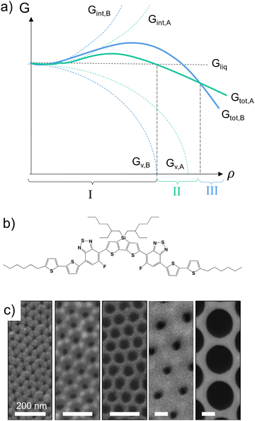
Molecular semiconductors have attracted significant attention for the fabrication of a range of optoelectronic devices, such as transistors, light-emitting diodes, sensors or photovoltaic devices,1,2 often used in thin-film structures of a thickness of 100 nm or less, where confinement effects may occur. As for many materials, especially organic small molecules, molecular semiconductors frequently display a multitude of polymorphs, their formation being dictated by both kinetic and thermodynamic factors. Classical crystal nucleation theory3–5 can thereby be used to describe the thermodynamics of molecular semiconductor polymorph formation considering that, simplistically, the development of any crystalline solid can be defined by the sum of the positive interfacial free energy change, ΔGint, and the negative volume free energy change, ΔGV, i.e., the total free energy change, ΔGtot. Importantly, the phase with the lowest Gtot is the most thermodynamically stable one at any given time of the process. This is illustrated in Fig. 1a for a scenario where a liquid (region I) transforms into a solid via an initial polymorph A (region II), before a structure dominated by polymorph B develops (region III).A typical example for such a scenario is given by the small molecular donor material, p-DTS(FBTTh2)2 (see Fig. 1b for the chemical structure),6 for which a short-lived crystal phase, a low-Gint polymorph, was found at the start of solidification, which then evolved into a second polymorph, a low-GV polymorph, as time advanced.7–10 This observation indicates that polymorphs with low Gint (higher GV) are preferred when the p-DTS(FBTTh2)2 crystallites still are very small, while at a later stage, when crystals grow, GV is low (Gint is high), resulting in a different total free energy, Gtot, profile.
Here, we explore whether this finding can be exploited for the “screening” of polymorphs in molecular materials, especially when confined in small volumes as found in many thin-film structures, employing p-DTS(FBTTh2) as a model system and using the fact that the formation of low-Gintvs. low-GV p-DTS(FBTTh2) polymorphs depends on crystal size, ρ (Fig. 1a). We focus on nano-confinement in nanoporous anodic aluminium oxide (AAO) host matrices (diameters ranging from 25 to 400 nm; see Fig. 1c and ESI,† Fig. S1) that have been shown to enable control of the lateral crystal size of organic semiconductors, including p-DTS(FBTTh2).11 Specifically, only crystals of limited dimensions form in AAOs comprising small pores (<60 nm);11 hence, it can be assumed that Gint is the major contribution to Gtot,4,5,12–15—a fact that should allow us to mimic the early-stage solidification process of materials such as p-DTS(FBTTh2). [Information about the materials and sample-preparation procedures used in this work are included in the ESI.†]
Results and discussion
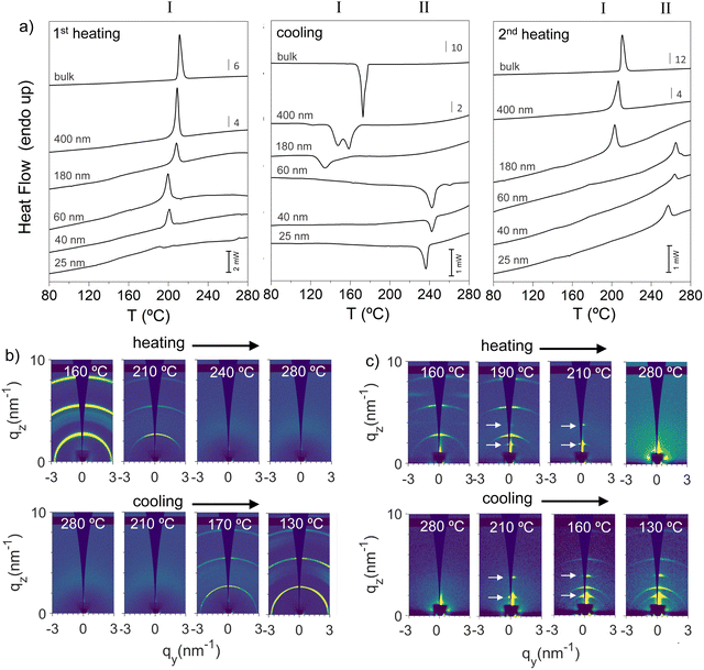
We begin describing the infiltration of p-DTS(FBTTh2)2 into AAOs. A very convenient pathway is to melt p-DTS(FBTTh2)2 at temperatures above 240 °C on the surface of the AAO nanoporous matrices, which results in a spontaneous flow of p-DTS(FBTTh2)2 into the open pores,16 filling the AAOs within the time frame of seconds to a few minutes. Beneficially, in cases where the residual p-DTS(FBTTh2)2 on the template surface is removed after pore infiltration, only p-DTS(FBTTh2)2 inside the nanopores remains. Crystallization of the organic semiconductor in nanoscale confinement can, thus, be studied without effects of heterogenous nucleation that would be caused by, e.g., a DTS(FBTTh2)2 surface layer (see the ESI† for details on the process and characterization).Characterizing with differential scanning calorimetry, DSC, p-DTS(FBTTh2)2-filled nanoporous AAOs with removed sacrificial layers, using pore diameters of 25, 40, 60, 180 and 400 nm (Fig. 1c), immediately reveal clear signs of polymorphism. Fig. 2a shows the heat flow rate recorded during the 1st heating and cooling scans, as well as the 2nd heating thermograms, taken at a rate of 20 °C min−1. While all samples exhibit in the 1st heating thermograms a single endotherm around 200 °C (Fig. 2a, left), which is attributed to the melting of p-DTS(FBTTh2)2 phase I crystals,11 a notable difference in the solidification behavior of p-DTS(FBTTh2)2 during cooling is observed depending on whether AAOs with small or large pores are used. For p-DTS(FBTTh2)2 confined in large pores (diameter larger than 60 nm), intense exotherms in the temperature range between 130 and 180 °C are observed that can be associated with the crystallization of p-DTS(FBTTh2)2 into the common phase I crystals (Fig. 2a, middle panel). In contrast, in AAOs with smaller pores (pore size smaller than 60 nm), an exotherm is found at notably higher temperatures (around 240 °C) resulting in a solid that, upon further heating (2nd heating scan), melts at around 260 °C, which is a much higher temperature compared to the melting of p-DTS(FBTTh2)2 phase I crystals (around 215 °C; Fig. 2a, right panel). [Thermogravimetric analysis shown in Fig. S2 of the ESI† reveals that no thermal degradation occurs in the temperature range analyzed.]
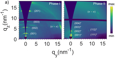
More detailed information of the two different p-DTS(FBTTh2)2 phases that form when confined in AAOs were obtained via grazing incidence X-ray scattering (GIWAXS), focusing on two samples: bulk p-DTS(FBTTh2)2vs. material confined in AAOs comprising pores of a 60 nm diameter (see Fig. 2b and c; the experimental geometry that was used for this analysis is depicted in Fig. S3 of the ESI†). We find that bulk p-DTS(FBTTh2)2 displays reflections characteristic for the phase I polymorph (see ESI,† Fig. S4), with the reflections disappearing above 210 °C upon heating indicating melting, and re-appearing upon cooling around 170 °C (Fig. 2b) signifying crystallization, in agreement with our DSC data. In strong contrast, for p-DTS(FBTTh2)2 confined in 60 nm diameter pores, besides the reflections attributed to phase I, additional reflections are recorded at qz ≈ 0.18 Å−1 and qz ≈ 0.36 Å−1 both during heating and cooling. These reflections, highlighted in Fig. 2c with arrows, suggest that another polymorph—termed hereafter p-DTS(FBTTh2)2 phase II—is formed that is different from phase I, as is evident also from the notably higher melting temperature of this p-DTS(FBTTh2)2 crystal form, clearly visualized by polarized optical microscopy, POM, by the disappearance of any birefringence above 270 °C (see Fig. S5 of the ESI;† note that POM, upon heating, reveals another phase transformation around 200 °C, detected by the change in the birefringence pattern – a transition that is only faintly visible in the thermal analysis data presented in Fig. 2a).
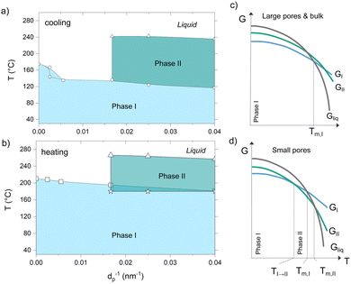
Combining our results from GIWAXS, DSC and POM, we went on and established the temperature–confinement (T–C) phase diagrams that summarize the phase behavior of p-DTS(FBTTh2)2 as a function of the temperature and the degree of spatial confinement (here given as the inverse of the pore diameter, d−1; Fig. 3a and b), identifying the T–C space where the different crystalline phases are observed. Specifically, at a given degree of confinement, i.e. above a certain value of d−1, the p-DTS(FBTTh2)2 phase I does not directly transform into a melt, but rather evolves into another solid crystal arrangement, p-DTS(FBTTh2)2 phase II. This phase behavior can be rationalized with the energy diagrams shown in Fig. 3c and d. Within small pores (smaller than 60 nm, Fig. 3d), phase I is the thermodynamically stable form at low temperatures (light blue region in Fig. 3a and b), while phase II is the stable form at elevated temperatures prior to melting (dark green region in Fig. 3a and b). In large pores and in the bulk (Fig. 3c), however, no temperature range exists in which phase II is thermodynamically stable; hence, phase I turns directly into the liquid state at the melting temperature.
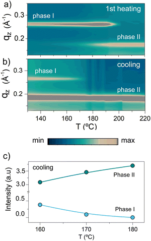
Such a behavior means that phase I and phase II are enantiotropically related, i.e. both of them are thermodynamically stable in their respective temperature regimes.17 Azimuthally integrated GIWAXS data displayed in Fig. 4, which show the reflection intensities observed during heating and cooling, are in agreement with such a conclusion. In the heating experiment shown in Fig. 4a, the (001) reflection of phase I crystals, recorded at qz ≈ 0.26 Å−1, is the only visible feature at low temperatures. Upon further heating up to temperatures slightly lower than the melting temperature of phase I, i.e. below ≈215 °C, the phase II reflection at qz ≈ 0.18 Å−1 starts to appear, indicating that at least a fraction of phase I crystals undergo a solid–solid phase transition to phase II. The view that the transformation from phase I to phase II is a reversible solid–solid phase transition is supported by the fact that during subsequent cooling (Fig. 4b and c), the scattered intensity of the (001) reflections from phase I increases, while that of phase II reflections decreases; i.e., phase I develops from phase II crystals and vice versa. However, we stress that these transformations can be kinetically hindered as it is described in detail in the ESI† (Fig. S6 and S7), along a more-detailed discussion about the nature of the observed transition. Indeed, while POM (Fig. S5, ESI†) indicates a transition from one phase to another around 200 °C, as evidenced by the appearance of a different birefringence pattern, this transition is barely detectable in DSC (Fig. 2a), likely due to the small enthalpy change related to it. Such a picture is in agreement with simulations of the GIWAXS data presented in Fig. 5 (the crystal lattice proposed for phase I and phase II and the indexation of the GIWAXS reflections are provided in the ESI† in Fig. S8 and S9, respectively18), which are dominated for both crystal forms by equidistant, intense reflections along the z-axis. In particular, phase I and phase II are based on periodic layered structures featuring a triclinic unit cell, in which the aromatic backbones and ethyl-hexyl side chains at the dithienosilole units periodically alternate along the c-axis, as illustrated in Fig. S10 of the ESI.† However, the lattice in phase II is expanded along the c-axis (from 2.2 to 3.3 nm) and compressed along the b-axis (from 1.5 to 1.2 nm) compared to the one of phase I. Furthermore, the π–π stacking plane is shifted to a smaller value of α than in phase I, with α being the angle between the π–π stacking planes and the (001) planes. In agreement with this, Raman spectroscopy (data shown in Fig. S11 of the ESI†) reveals relative scattered intensity variations between polymorphs I and II, including two low frequency (200–500 cm−1) modes that evolve when phase II is dominant. Density functional theory (DFT) calculations performed on an isolated p-DTS(FBTTh2)2 molecule in vacuum and with its side chains substituted by methyl groups (Fig. S12 of the ESI†) suggest that these relative intensity variations and low frequency modes can be attributed to distinct conformations and bending modes of the lateral benzothiadiazole (BT) and thiophene (T) units, underpinning the view that more room (“free volume”) for the BT and T moieties to deform is provided in polymorph II.
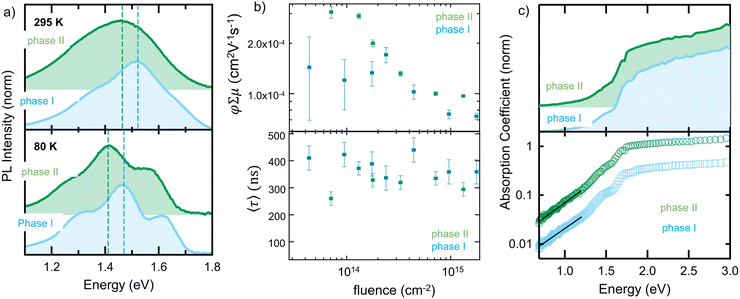
The importance of understanding the phase behavior of molecular semiconductors becomes clear when analyzing the optoelectronic properties of the phase I- and phase II- polymorphs. Distinct differences in the photoluminescence, PL (Fig. 6a; spectra taken at 295 K and 80 K), between phase I and phase II in a nanoconfined (25 nm pores) p-DTS(FBTTh2)2 are found. Pertinently, a red-shift of ∼0.06 eV in the phase II peak maximum relative to phase I (≈1.48 eV) is recorded at both temperatures, accompanied by an increase in the intensity ratio between the 0-0 to 0-1 transitions (from ≈0.55 to ≈0.67). Taken together, the two spectral changes (red-shift and greater 0-0/0-1 ratio) in phase II relative to phase I are consistent with transition dipoles in the former having a more head-to-tail orientation (i.e., more J-type aggregation),19 although changes in dielectric environment may also contribute to the observed red-shift.
Differences in the charge-transport properties of the two polymorphs, as measured in time-resolved microwave conductivity (TRMC) experiments, are also found. Fig. 6b shows the fitting parameters for the microwave conductivity transients (which are shown in Fig. S13 of the ESI†) as a function of fluence for both crystal forms: the sum of the pre-exponential factors in the top panel of Fig. 6b and the amplitude-weighted average time-constant in the bottom panel of Fig. 6b. While it is not possible to independently assign a specific charge-carrier mobility or yield from these data, they do provide a lower-limit on the mobility as the yield must be less than 1. Tellingly, we find that the yield-mobility product of phase II is approximately double that of phase I (confined in 25 nm pores) at low excitation fluence, highlighting the importance of controlling polymorph formation.
Conclusions
We showed here that the confinement within dimensions relevant in thin-film electronics, is one of the key determining factors that can be used to manipulate Gint and, in turn, polymorph formation. We focused on p-DTS(FBTTh2)2, which is a material of a rich conformation landscape (see Fig. S12, ESI†) owing, among others, to the fact that the thiophenes adjacent to the benzothiadiazole units have no or little preference to face “up” or “down”.20,21 When solidifying DTS(FBTTh2)2, under high degrees of spatial restriction – i.e. at small pore size – and high temperatures, a crystal form develops that is not observed under weak confinement or in the bulk. Intriguingly, a two-fold increase of the yield-mobility product is observed in phase II, despite the fact that p-DTS(FBTTh2)2 molecules are similarly packed in both phases. Our approach thus allows screening for new, high-performing polymorphs. We would like to note though that confinement can lead to an increase in the number of defect states (and hence sub-bandgap transitions). This can be deduced from photothermal deflection spectroscopy, PDS, measurements, which rely on the absorption-induced heating to deflect a laser passing parallel to the substrate. Fig. 6c shows the (normalized) absorption coefficient for both polymorphs, presented on linear and logarithmic vertical axes. Although the spectrum from phase II is very similar to that of phase I (confined in 25 nm pores), with broad absorption above 1.8 eV, the vibronic structure (i.e., peak shoulders at ∼1.5 and ∼1.7 eV) is slightly more pronounced in phase I than phase II. Particularly noticeable is the very shallow absorption tail, which yields an Urbach energy, Eu, (by fitting with α(E) = exp((E − E0)/Eu) between 0.7 and 1.2 eV) of ∼0.37 eV (for phase I) and ∼0.35 eV (for phase II). A comparison with Eu values for other conjugated materials22,23 reveals that these are between 5 and 10 times larger than typical figures, due to a substantial increase in the number of defect states (and hence sub-bandgap transitions) regardless of the polymorph. That said, confined material growth is highly useful and relatively straight-forward to achieve. This approach, thus, will assist in understanding polymorphism in molecular semiconductors towards more reliable and reproducible processing and fabrication of organic optoelectronic devices.Conflicts of interest
There are no conflicts to declare.Acknowledgements
This work is supported by MCINN/FEDER (under ref. PID2021-126243NB-I00 and PGC2018-095411-B-I00) and Xunta de Galicia (Proyectos de Consolidación ref. ED431F 2021/009). J. M. thanks MCINN for the Ramón y Cajal contract. N. S. in addition gratefully acknowledges support from the IdEx Bordeaux Excellence program (ANR-10-IDEX-03-02). The authors would like to acknowledge the financial support provided by the IONBIKE RISE project. This project has received funding from the European Union's Horizon 2020 research and innovation programme under the Marie Skłodowska-Curie grant agreement no. 823989. All authors acknowledge the synchrotron radiation source ELETTRA (Trieste, Italy) for providing beam time and the staff from the SAXS beamline for support. This work was authored in part by the National Renewable Energy Laboratory, operated by Alliance for Sustainable Energy, LLC, for the U. S. Department of Energy (DOE) under Contract No. DE-AC36-08GO28308. Funding for TRMC measurements was provided by the Solar Photochemistry Program, Division of Chemical Sciences, Geosciences, and Biosciences, Office of Basic Energy Sciences, U. S. Department of Energy. The views expressed in the article do not necessarily represent the views of the DOE or the U. S. Government. The U. S. Government retains and the publisher, by accepting the article for publication, acknowledges that the U. S. Government retains a nonexclusive, paid-up, irrevocable, worldwide license to publish or reproduce the published form of this work, or allow others to do so, for U. S. Government purposes. J. M. thanks MICINN/FEDER for the Grant PID2021-126243NB-I00.References
- S. Karuthedath, S. H. K. Paleti, A. Sharma, H. Yin, C. S. P. De Castro, S. Chen, H. Xu, N. Alshehri, N. Ramos, J. I. Khan, J. Martin, G. Li, F. Laquai, D. Baran and J. Gorenflot, Adv. Energy Mater., 2023, 13, 2203464 CrossRef CAS.
- E. Gutierrez-Fernandez, A. D. Scaccabarozzi, A. Basu, E. Solano, T. D. Anthopoulos and J. Martín, Adv. Sci., 2022, 9, 2104977 CrossRef CAS PubMed.
- M. Volmer, Kinetic der Phasenbildung, Steinkoopff, Dresden, Leipzig, 1939 Search PubMed.
- B. D. Hamilton, J.-M. Ha, M. A. Hillmyer and M. D. Ward, Acc. Chem. Res., 2012, 45, 414–423 CrossRef CAS PubMed.
- G. T. Rengarajan, D. Enke, M. Steinhart and M. Beiner, Phys. Chem. Chem. Phys., 2011, 13, 21367–21374 RSC.
- L. A. Perez, K. W. Chou, J. A. Love, T. S. van der Poll, D.-M. Smilgies, T.-Q. Nguyen, E. J. Kramer, A. Amassian and G. C. Bazan, Adv. Mater., 2013, 25, 6380–6384 CrossRef CAS PubMed.
- Q. Cui, Y. Hu, C. Zhou, F. Teng, J. Huang, A. Zhugayevych, S. Tretiak, T.-Q. Nguyen and G. C. Bazan, Adv. Funct. Mater., 2018, 28, 1702073 CrossRef.
- L. Nian, K. Gao, Y. Jiang, Q. Rong, X. Hu, D. Yuan, F. Liu, X. Peng, T. P. Russell and G. Zhou, Adv. Mater., 2017, 29, 1700616 CrossRef PubMed.
- T. S. van der Poll, J. A. Love, T.-Q. Nguyen and G. C. Bazan, Adv. Mater., 2012, 24, 3646–3649 CrossRef CAS PubMed.
- L. A. Perez, J. T. Rogers, M. A. Brady, Y. Sun, G. C. Welch, K. Schmidt, M. F. Toney, H. Jinnai, A. J. Heeger, M. L. Chabinyc, G. C. Bazan and E. J. Kramer, Chem. Mater., 2014, 26(22), 6531–6541 CrossRef CAS.
- J. Martín, M. Dyson, O. G. Reid, R. Li, A. Nogales, D.-M. Smilgies, C. Silva, G. Rumbles, A. Amassian and N. Stingelin, Adv. Electron. Mater., 2018, 4, 1700308 CrossRef.
- M. Beiner, J. Polym. Sci., Part B: Polym. Phys., 2008, 46, 1556–1561 CrossRef CAS.
- B. D. Hamilton, M. A. Hillmyer and M. D. Ward, Cryst. Growth Des., 2008, 8, 3368–3375 CrossRef CAS.
- J.-M. Ha, B. D. Hamilton, M. A. Hillmyer and M. D. Ward, Cryst. Growth Des., 2009, 9, 4766–4777 CrossRef CAS.
- J.-M. Ha, J. H. Wolf, M. A. Hillmyer and M. D. Ward, J. Am. Chem. Soc., 2004, 126, 3382–3383 CrossRef CAS PubMed.
- M. Steinhart, J. H. Wendorff, A. Greiner, R. B. Wehrspohn, K. Nielsch, J. Schilling, J. Choi and U. Gosele, Science, 2002, 296, 1997 CrossRef CAS PubMed.
- K. Kawakami, J. Pharm. Sci., 2007, 96, 982–989 CrossRef CAS PubMed.
- J. A. Love, C. M. Proctor, J. Liu, C. J. Takacs, A. Sharenko, T. S. van der Poll, A. J. Heeger, G. C. Bazan and T.-Q. Nguyen, Adv. Funct. Mater., 2013, 23, 5019–5026 CrossRef CAS.
- F. C. Spano, Acc. Chem. Res., 2010, 43, 429–439 CrossRef CAS PubMed.
- C. B. Nielsen, A. J. P. White and I. McCulloch, J. Org. Chem., 2015, 80, 5045–5048 CrossRef CAS PubMed.
- H. Bronstein, J. M. Frost, A. Hadipour, Y. Kim, C. B. Nielsen, R. S. Ashraf, B. P. Rand, S. Watkins and I. McCulloch, Chem. Mater., 2013, 25(3), 277–285 CrossRef CAS.
- A. J. Kronemeijer, V. Pecunia, D. Venkateshvaran, M. Nikolka, A. Sadhanala, J. Moriarty, M. Szumilo and H. Sirringhaus, Adv. Mater., 2014, 26, 728–733 CrossRef CAS PubMed.
- D. Venkateshvaran, M. Nikolka, A. Sadhanala, V. Lemaur, M. Zelazny, M. Kepa, M. Hurhangee, A. J. Kronemeijer, V. Pecunia, I. Nasrallah, I. Romanov, K. Broch, I. McCulloch, D. Emin, Y. Olivier, J. Cornil, D. Beljonne and H. Sirringhaus, Nature, 2014, 515, 384 CrossRef CAS PubMed.
Footnote |
| † Electronic supplementary information (ESI) available. See DOI: https://doi.org/10.1039/d3tc03640e |
| This journal is © The Royal Society of Chemistry 2024 |

