
 Open Access Article
 This Open Access Article is licensed under a
 Creative Commons Attribution 3.0 Unported Licence
Recent advances in atomic layer deposition of superconducting thin films: a review
Getnet Kacha Deyu
 *a,
Marc Wenskatab,
Isabel González Díaz-Palacioac,
Robert H. Blickc,
Robert Zieroldc and
Wolfgang Hillerta
*a,
Marc Wenskatab,
Isabel González Díaz-Palacioac,
Robert H. Blickc,
Robert Zieroldc and
Wolfgang Hillerta
aInstitute of Experimental Physics, Universität Hamburg, Luruper Chaussee 149, D-22761, Hamburg, Germany. E-mail: getnet.kacha.deyu@desy.de
bDeutsches Elektronen-Synchrotron DESY, Notkestrasse 85 D-22607, Hamburg, Germany
cInstitute for Nanostructure and Solid State Physics & Center for Hybrid Nanostructures, Universität Hamburg, Luruper Chaussee 149, D-22761, Hamburg, Germany
First published on 9th May 2025
Abstract
The development of superconducting thin films has opened new avenues in electronic and quantum technologies, offering potential breakthroughs in performance due to their unique properties such as zero electrical DC resistance and perfect diamagnetism. Atomic layer deposition (ALD) stands out as a highly precise and uniform technique for fabricating these films based on sequential, and self-limiting gas-solid surface reactions, offering distinct advantages over other deposition methods. This review explores the role of ALD in the production of superconducting thin films, highlighting its ability to control film thickness at the atomic level, ensuring superior uniformity and conformality. The fundamentals of superconductors and the ALD process are discussed, along with a review of various materials used in the field. It also examines the existing and potential applications of these films and considers future prospects and challenges in the field.
 Left to right: Marc Wenskat (MW), Robert Zierold (RZ), Wolfgang Hillert (WH), Getnet Kacha Deyu (GD), Isabel González Díaz-Palacio (IP), Robert H. Blick (RB) | Established in 2018, the collaborative consortium among the Institute of Experimental Physics (IEP–WH, MW, IG, GD) and the Center for Hybrid Nanostructures (CHyN–RB, RZ, IG), both at the University of Hamburg, along with the Deutsches Elektronen-Synchrotron (DESY–MW), targets research into the future of superconducting radio-frequency (SRF) cavities. Making use of the broad expertise in accelerator physics (WH), state-of-the-art SRF cavity design (MW), advanced materials science (GD, IG, RZ), and quantum transport physics (RB), the consortium is well positioned to tackle key challenges in this field. The collaboration, focusing on superconductor–insulator–superconductor structures, utilizes atomic layer deposition to improve cavity performance, with the goal of pushing the limits of next-generation accelerators. The synergy between the University of Hamburg's famous experimental capabilities at IEP and CHyN together with DESY's accelerator facilities enables the group to pioneer advancements. This partnership not only reflects a strong commitment to scientific excellence but also underscores the critical importance of multidisciplinary collaboration in driving forward technological innovations crucial for the future of high-energy physics and material science research and bringing the methods for fabricating superconducting thin film materials to the next level. |
Wider impactThis article is expected to generate significant interest within the materials science community due to the rising focus on atomic layer deposition (ALD) as a precise method for fabricating superconducting thin films. ALD's ability to deposit films with atomic-scale precision enables unparalleled control over microstructure, which is critical for optimizing superconducting properties. Recent advancements have demonstrated ALD's potential for improving film uniformity, interface quality, and composition control, making it a transformative tool for applications in quantum computing and high-frequency electronics. Additionally, ALD's scalability and ability to coat complex geometries distinguish it from other deposition techniques, positioning it as a key enabler for the large-scale manufacturing of superconducting devices. Despite the growing research in this field, a comprehensive review on ALD for superconducting films is still lacking. This work fills that gap by providing a detailed overview of superconducting ALD processes, recent breakthroughs, and emerging applications. It also identifies critical challenges, such as material selection, deposition conditions, and integration with device architectures. By outlining future research directions, this review serves as a valuable resource for both academia and industry, guiding efforts toward next-generation superconducting technologies and shaping the future of materials science through ALD-driven innovations. |
1 Introduction
1.1 Quest for thin film superconductors
Superconducting materials exhibit extraordinary electrical and magnetic properties that make them ideal for various high-performance applications, including quantum computing, magnetic sensing, advanced electronics and particle accelerators (cavities and magnets) or medical diagnostics (magnetic resonance imaging-MRI). The development of thin film superconductors aims to harness these properties in compact, scalable formats suitable for integration into various devices. Thin films enable the exploration of new superconducting phenomena and improve device performance by reducing size and weight while preserving or enhancing superconducting properties. Additionally, thin films offer advantages such as flexibility, reduced material usage, and easier integration into complex circuits. However, this pursuit is not without its challenges. As the thickness of a superconducting film decreases, it becomes increasingly difficult to maintain its critical temperature—the point at which the material becomes superconducting. Defects, impurities, and grain boundaries in the thin films can disrupt the superconducting state. Furthermore, the interaction between the film and its substrate can cause strain and alter the materials electronic properties, complicating the preservation of superconductivity.Despite these challenges, thin film superconductors have found critical applications in various advanced technologies. They are essential in the fabrication of superconducting quantum interference devices (SQUIDs),1 which are used in highly sensitive magnetometers. In quantum computing, thin film superconductors are used to create qubits,2–4 the fundamental units of quantum information. These films are also employed in high-performance microelectronics,5 where they enable faster and more efficient components.
Recent advancements have focused on finding new materials that can sustain superconductivity at higher temperatures and in thinner films. In parallel, significant efforts are being directed towards enhancing the scalability and robustness of thin film superconductors, with proper fabrication techniques playing a crucial role in achieving these goals.6 Although challenges persist, the progress made to date has already driven significant advancements across various high-tech industries. As research continues, thin film superconductors are set to become integral to the future of quantum computing, energy-efficient technologies, medical imaging, and more.
1.2 Significance of fabrication techniques
For most current and future applications of materials in advanced technologies, it is essential to fabricate the active material as high-quality thin films or conformal coatings. Conventional physical vapor deposition (PVD) methods are suitable for thicker layers. However, for layers thinner than 50 nm, these methods are not viable due to issues with conformality.7 While chemical vapor deposition (CVD) has been explored as a solution, challenges such as controlling nucleation, ensuring strong interfacial adhesion of metals to common barrier layers on various substrates, and the toxicity, scarcity, and difficult handling of precursors (the chemical substances that are introduced into the reaction chamber) have limited its success. Atomic layer deposition (ALD), the state-of-the-art thin-film technology, has proven to be superior in overcoming many of these challenges, particularly in advanced applications. ALD can produce highly conformal thin films that adhere perfectly to even the most complex 3D surface architectures with nanometer precision.7–9Superconducting thin films require precise control over thickness, composition, and uniformity to achieve optimal performance. ALD has become a preferred method because it enables atomic-level precision and excellent conformality, even on complex geometries. Unlike traditional techniques such as sputtering or CVD, ALD allows for controlled material growth at low temperatures, thereby preserving the integrity and superconducting properties of sensitive films.
1.3 Scope of the review
Despite the growing interest in this topic, there is a lack of comprehensive reviews on the use of ALD for depositing superconducting thin films. This overview seeks to address that gap by presenting the current state of research in the field. It specifically highlights the ALD processes developed for coating various superconducting materials and explores the wide range of applications for these coated films in high-performance environments. Furthermore, this review examines the challenges and future directions in the field, with an emphasis on areas needing further research and development.2 Superconductors in brief
2.1 Fundamentals of superconductivity
Superconductivity was first discovered in 1911 by H. Kamerlingh-Onnes while examining materials like mercury, lead, and tin. He found that these materials exhibited vanishing electrical DC resistance below a specific critical temperature, known as Tc. This discovery came after he successfully liquefied helium and investigated the behavior of electrical resistivity. Kamerlingh-Onnes measured the resistance of a mercury sample as the temperature changed and observed a sharp drop to a level indistinguishable from zero ≈4 K. He named this phenomenon superconductivity. In the 1950s, the BCS theory, developed by Bardeen, Cooper, and Schrieffer, provided a comprehensive theoretical framework for classical superconductors. This advancement led to the discovery of numerous elements and compounds that display superconducting properties. In addition to BCS theory, the Ginzburg–Landau Theory and the London equations also contributed to our understanding of superconductivity. While BCS theory is a microscopic model, Ginzburg–Landau offers a more thermodynamic perspective, akin to the Bose–Einstein condensation (BEC) approach. The London equations, originating in the 1930s, represent the earliest theoretical model in this field.10,11 | ||
| Fig. 1 (a) Diagram illustrating the Meissner effect, where the blue sphere represents a superconductor. (b) Representation of the coherence length (ξ) and penetration depth (λ) at the boundary between a normal region and a superconducting one for Type I and Type II superconductors. (c) Magnetization as a function of applied field for Type I and Type II superconductors. | ||
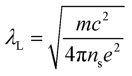
2.1.2.1 London theory. In 1935, Fritz and Heinz London quantitatively analyzed the ability of superconductors to expel magnetic fields,13 building on the two-fluid model by Gorter and Casimir.10,11,14 This model describes how, below the (Tc), a fraction of conduction electrons, ns(T), forms a supercurrent that flows without resistance, while the remaining electrons, n − ns(T), behave as a normal fluid incapable of carrying current without resistance. The Londons showed that the magnetic field does not vanish abruptly at a superconductor's surface but instead decreases exponentially into the bulk, characterized by the London penetration depth, λL, which in most pure metals is typically on the order of 10 to 100 nm. The magnetic flux at a distance x inside the superconductor follows the relationship:
 | (1) |
 | (2) |
2.1.2.2 The BCS theory. In 1957, Bardeen, Cooper, and Schrieffer proposed the BCS theory, providing a microscopic explanation for superconductivity.15 This theory posits that superconductivity arises from an attractive interaction between electrons near the Fermi surface, mediated by lattice vibrations known as phonons. When electrons traverse a metal, they distort the lattice, generating a positively charged region that attracts another electron, resulting in the formation of a Cooper pair. These pairs form when the energies of two electrons are close to the Fermi energy, within an energy range approximately equal to the Debye energy, ħωD, which corresponds to the typical phonon energy. Acting as bosons, Cooper pairs can occupy the same quantum state, avoiding the restrictions of the Pauli Exclusion Principle. Collectively, these pairs create a ground state where each electron influences the available wave vectors and contributes to the pairing process. The spatial extent of a pair's wave function is known as the coherence length, ξ0.
The Cooper pair interaction can be broken by thermal activation, leading to the concept of the superconducting energy gap (Δ). This gap represents the energy required to restore a superconducting electron to its normal state and is expressed at T = 0 as:
 | (3) |
Type I superconductors such as Pb, Hg, and Zn have a positive surface energy at the boundary, which results in a complete expulsion of magnetic fields (Meissner effect) until a critical field Hc is reached. Beyond Hc, they transition abruptly to a normal state, see Fig. 1(b) and (c).
Type II superconductors, such as Nb, TiN, NbN, and NbTiN, have a negative surface energy, making it favorable to form superconducting-normal boundaries. They fully expel the magnetic field up to a lower critical field Hc1, then enter a mixed state where magnetic flux vortices form. The density of these vortices increases until the superconducting state is destroyed at the upper critical field Hc2, see Fig. 1(c).
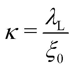
2.1.3.1 Ginzburg–Landau parameter. Ginzburg–Landau Theory gives a quantitative description of superconductors near the transition point.10,11 A superconductor type is defined by the Ginzburg–Landau (GL) parameter κ as:
 | (4) |
The distinction between the two types of superconductors is as follow:
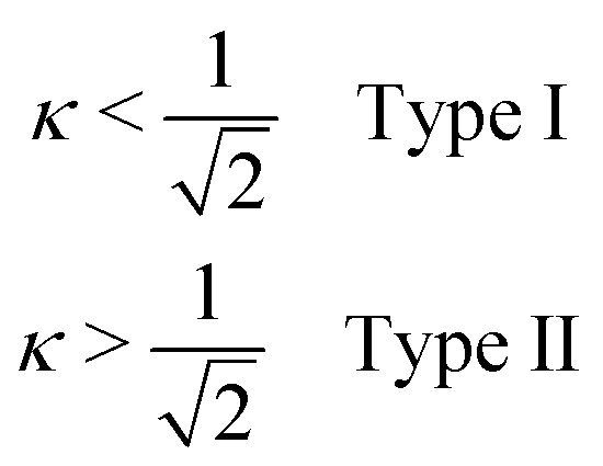 | (5) |
2.1.3.2 Critical fields. The elementary BCS prediction for the temperature dependence of
![[script letter H]](https://www.rsc.org/images/entities/char_e142.gif) c(
c(![[scr T, script letter T]](https://www.rsc.org/images/entities/char_e533.gif) ) is often expressed by using the empirical formula:
) is often expressed by using the empirical formula:
 | (6) |
Eqn (6) is valid for temperatures in the range of 0 ≤ T ≤ Tc.
2.1.4.1 Surface resistance. At temperatures above absolute zero, a fraction of normal electrons remains unpaired, which can potentially dissipate energy if set into motion. In the DC regime, superconductors exhibit zero electrical resistance because Cooper pairs fully take over charge transport. However, in the RF regime, a time-varying electric field is present, which forces both normal electrons and Cooper pairs into oscillatory motion. As normal electrons move, they contribute a non-zero resistance to the material. As this movement is confined in a thin surface layer (skin effect) the according resistance is called surface resistance (Rs) and consists of two main components:
| Rs = RBCS(T) + Rres | (7) |
The BCS surface resistance (RBCS) turns out to be a temperature and frequency dependent. In contrast, the residual surface resistance (Rres) is temperature-independent and arises from parasitic losses, though its precise origin remains unclear. Both intrinsic factors—such as non-ideal surface quality, metallic inclusions, surface oxides, and grain boundaries—and accidental mechanisms, like particulates, chemical residues, or surface defects, contribute to these losses. Additionally, extrinsic factors, such as flux trapped during cooling, play a role. Given the diversity of contributing phenomena, Rres cannot be predicted with a single formula. However, empirical studies suggest that Rres is at least proportional to rn, the normal-state resistance. Between two materials with identical BCS resistance, the one with a lower rn typically exhibits smaller residual resistance.
2.1.4.2 Residual resistivity ratio (RRR). Is a key measure of metal purity, which is expressed as the ratio of electrical resistivity at 295 K to that at 0 K. For SRF cavities, a minimum RRR of 200 is required, while high-gradient cavities typically have an RRR of 300.16 Impurities such as oxygen, nitrogen, hydrogen, and carbon (O, N, H, C) act as scattering centers for conduction electrons, reducing RRR and thermal conductivity.17
3 Atomic layer deposition
3.1 Fundamentals
Atomic layer deposition (ALD) is a vapor-phase deposition technique renowned for its capability to synthesize ultra-thin films. These films are typically grown sub-monolayer by sub-monolayer, achieved through the repeated execution of two distinct half-reactions.8,18–25 The principles of ALD can be illustrated by considering the deposition of superconducting TiN, as shown in the schematics of Fig. 2. In a typical ALD process, alternating pulses of gaseous chemical precursors react with the substrate surface in a sequential manner. For instance for TiN deposition, this can be achieved using either thermal or plasma-enhanced ALD (PEALD) systems. In thermal ALD, TiCl4 and NH3 are the common precursors,5,26 whereas in PEALD, TiCl4 is combined with H2/N2-plasma.27 Each precursor pulse introduces a half-reaction, during which the precursor reacts with the substrate in a self-limiting manner, ensuring that only a maximum of monolayer of material per cycle is deposited. After each precursor pulse, the chamber is purged with an inert carrier gas, such as nitrogen (N2) or argon (Ar), to remove any unreacted precursor or reaction by-products. The process is then repeated with a counter-reactant precursor—such as NH3 or H2/N2-plasma—in the next half-reaction. This cycle continues until the desired TiN film thickness is achieved.5,26,27 The self-limiting nature of ALD allows for precise control over film thickness, uniformity, and quality, making it an ideal technique for growing materials.8,18–25 However, the process faces challenges due to steric and electrostatic hindrance from ligands, particularly those associated with the chemisorbed first reactant. This hindrance can shield portions of the surface, limiting accessibility for the second reactant. As a result, the growth per cycle (GPC) in ALD, especially when using compound reactants like those examined in this review, is often significantly less than a full monolayer. Experimental GPC values exhibit variability up to 30% of a monolayer, contingent upon the growth temperature.19,28 Despite these challenges, ALD technology offers the possibility to prepare thin films of high quality materials with no line-of-sight deposition, precise thickness control, high uniformity, and excellent conformality. | ||
| Fig. 2 Schematic of ALD process for superconducting TiN films. (a) Substrate surface has natural functionalization or is treated to functionalize the surface. (b) Precursor A (TiCl4) is pulsed and reacts with surface. (c) Excess precursor and reaction by-products are purged with inert carrier gas. (d) Precursor B (NH3 or H2/N2-plasma) is pulsed and reacts with surface. (e) Excess precursor and reaction by-products are purged with inert carrier gas. (f) Steps 2–5 are repeated until the desired material thickness is achieved. Adopted from ref. 25. Copyright 2014, Elsevier Publishing. | ||
ALD processes are usually conducted at moderate temperatures (below 350 °C).25 The specific temperature range where growth is saturated is known as the “ALD temperature window” and varies depending on the process.19 Operating outside of this window can lead to poor growth rates and non-ALD-type deposition due to issues such as slow reaction kinetics or precursor condensation at low temperatures, and thermal decomposition or rapid desorption of the precursor at high temperatures. To maximize the advantages of ALD, it is crucial to operate within the designated ALD temperature window for each deposition process.19,25
3.2 Types of ALD
In general, when selecting an ALD process for depositing superconducting thin films, several critical criteria must be considered to achieve optimal performance. The material composition is paramount, as the superconducting properties depend on precise stoichiometry and phase purity, which necessitates the use of carefully chosen precursors that can deliver the desired elements in the correct ratios. Temperature control is crucial since the deposition temperature must be low enough to prevent degradation of the superconducting properties while still allowing for sufficient surface reactions. Additionally, film uniformity and conformality are essential, particularly for applications in microelectronics or quantum devices, where even slight variations in thickness can significantly impact device performance.29 The substrate compatibility is another key factor, as the substrate must not only withstand the deposition process but also have to ensure surface group termination. This surface termination is vital for enabling the self-limiting reactions that characterize ALD, ensuring uniform and controlled film growth. Finally, process throughput and scalability are important for commercial applications, where consistent and high-quality films need to be produced efficiently. Balancing these factors is essential to selecting the most suitable ALD process for superconducting thin films.There are several types of ALD processes, each optimized for different applications and materials. Below are some commonly used ALD methods, as well as others that show potential for application in the field of superconductivity, along with brief descriptions. The primary properties and superconducting materials deposited by these ALD techniques are summarized in Fig. 3.
 | ||
| Fig. 3 Comparison of main ALD process types, evaluated for coating uniformity and conformality, substrate compatibility, process throughput, and scalability. The table also outlines the advantages and disadvantages of each method and the reported materials of superconducting thin films. Star ratings (2, 3, and 4 stars) denote moderate, good, and excellent film uniformity and conformality, respectively. | ||
3.3 Comparison of ALD with other deposition techniques
ALD stands out among thin-film deposition techniques for superconducting materials due to its exceptional uniformity, conformality, and atomic level growth control. Unlike sputtering, arc-PVD, and spin coating, which suffer from poor conformality, ALD ensures a highly uniform and precise coating even on complex surfaces. Compared to CVD and pulsed laser deposition (PLD), which offer good film quality but lower conformality, ALD provides superior thickness control and defect-free layers. While Molecular Beam Epitaxy (MBE) also achieves atomic-level precision and excellent quality, it is significantly more expensive than ALD. In terms of cost, ALD is classified as a high-cost method due to its slow deposition rate, but it remains more affordable than MBE. Sputtering and PLD provide high-quality films at medium-to-high costs, whereas spin coating, dip coating, and spray pyrolysis are low-cost methods that result in lower film quality. Although ALD has a slow deposition rate, its ability to produce high-quality, uniform superconducting films makes it a preferred choice for applications requiring precision and reliability over speed and low-cost production.46–48 These comparisons are summarized in Table 1.| Technique | Deposition principle | Growth control | Uniformity | Conformality | Deposition rate | Temp. range (°C) | Cost | Film quality | SFf |
|---|---|---|---|---|---|---|---|---|---|
| a ALD – atomic layer deposition.b CVD – chemical vapor deposition.c MBE – molecular-beam epitaxy.d PLD – pulsed laser deposition.e Arc-PVD – cathodic arc deposition.f SF – selected superconducting films grown by the technique. | |||||||||
| ALDa | Self-limiting surface reactions | Atomic level precision | Excellent | Excellent | Slow | RT-400 | High | High | NbN, TiN, MoN5,30–33 |
| Sputtering | Plasma based physical deposition | Moderate | Good | Poor | Medium | RT-800 | Medium | High | NbN, MgB2, Nb3Sn49–51 |
| CVDb | Gas phase chemical reaction | Moderate | Good | Good | High | 300–1100 | High | High | BSCCO, MgB252–54 |
| MBEc | Atom by atom deposition in UHV | Atomic level | Excellent | Moderate | Slow | 200–800 | Very high | Very high | MgB2, SrFeAs55,56 |
| Spray pyrolysis | Aerosol precursor decomposition | Poor | Poor | Moderate | Medium | 200–600 | Low | Low-medium | MgB2,57 YBCO46,58 |
| Spin coating | Solution based film spreading | Poor | Moderate | Poor | Fast | RT-500 | Low | Low | YBCO59,60 |
| PLDd | Laser ablation of target | Good | Good | Moderate | Medium | 300–900 | High | High | FeSe/STO, Nb61,62 |
| Dip coating | Solution immersion | Poor | Poor | Poor | Fast | RT-300 | Low | Low | YBCO63 |
| Arc-PVDe | Cathodic arc vaporization | Moderate | Moderate | Poor | High | 200–800 | Medium | High | BSCCO, Pb, Nb64,65 |
4 ALD of superconductors
4.1 General observation
ALD has been successfully used to deposit various superconducting materials. Its capability to precisely control film thickness and composition makes it ideal for exploring the superconducting properties of thin films. However, compared to other deposition techniques, only a limited range of superconducting thin films have been reported using ALD. Generally, ALD can produce films with good superconducting properties, but careful optimization of deposition parameters is essential to achieve the desired results. This section will discuss and compare various reported ALD superconducting thin films with respect to their superconducting properties.4.2 Superconducting compounds
4.2.1.1 TiN. There are handful reports on superconducting TiN thin films grown using both thermal and plasma-enhanced ALD.3,5,27,38,77–79 The choice of precursors, deposition temperatures, film thicknesses, and specific deposition techniques have led to variations in the Tc of these films. Among these studies, the highest Tc of 4.62 K for TiN films grown using the ALD process was reported by Shearrow et al.38
Femi-Oyetoro et al.77 reported a superconducting TiN films grown by PEALD using tetrakis(dimethylamido)titanium (TDMAT) as the precursor and a nitrogen/argon mixture for the plasma step with a deposition temperature of 300 °C. In order to quantify the purity of grown films, they performed Secondary Ion Mass Spectrometer (SIMS) measurement, see Fig. 4(a). SIMS quantify the following impurities, H, C, and O levels of approximately 2.5%, 1%, and 0.3%, respectively. X-ray Photoelectron Spectroscopy (XPS) depth profiling indicated an average Ti:N ratio of 0.95. In addition, they examined the crystalinity of deposited films by Grazing Incidence-X-ray Diffraction (GI-XRD), see Fig. 4(b). The film show a crystalline structure with a preferred (111) orientation, with a measured lattice constant of 4.283 Å. High-resolution transmission electron microscopy (HRTEM) of an 80 nm TiN film showed columnar grain structures with grain widths up to 60 nm, see Fig. 4(da). X-ray diffraction (XRD) estimated crystallite sizes in various directions as 20 nm, 10 nm, 8 nm, and 7 nm. The overall film exhibited a smooth, multilayer structure, composed of a silicon nitride (SiNx) layer, a TiN nucleation layer, and a bulk TiN layer, as observed in the scanning transmission electron microscopy (STEM) image in Fig. 4(db). Furthermore, a 2 nm SiNx interface layer was detected between the TiN film and the silicon wafer, which was confirmed through energy-loss spectroscopy (EELS), Fig. 4(dc–f) and energy-dispersive spectroscopy (EDS), Fig. 4(dg). The formation of this interface layer was linked to the incubation period associated with nitrogen plasma exposure, which likely promotes silicon nitridation, a common phenomenon in nitrogen-based TiN growth processes. Fig. 4(c) compares the Tc between PEALD and sputtered TiN, with values of 4.35 K and 4.0 K, respectively. They attribute the lower Tc in their sputtered TiN to surface oxidation, intergranular voids, and a reduced N ratio.77
 | ||
| Fig. 4 TiN films grown by PEALD using TDMAT as the precursor and a nitrogen/argon mixture for the plasma step with a deposition temperature of 300 °C (a) SIMS spectra reveal contamination and composition profiles, displaying atomic concentrations of H, C, O, N, and Ti in an 80 nm PEALD TiN film. The TiN number density (1023 atoms per cc) serves as the basis for conversion to atom% units. (b) GI-XRD scan identifies the phase, with the inset showing the preferential (111) orientation at 2θ 36.5° of an 80 nm PEALD TiN film. (c) Resistance vs. temperature on 40 nm PEALD and sputtered TiN films demonstrates Tc values of 4.35 and 4.0 K, respectively.77 Copyright 2011, AIP Publishing. TiN films also grown by PEALD using TDMAT and N2 plasma as the precursor with a deposition temperature of 270 °C (e) Resistivity as a function of temperature for various TiN film thicknesses given by their quantities of ALD cycles. (f) SIMS of TiN film grown by ALD for 1250 cycles.38 Copyright 2018, AIP Publishing. TiN films grown via thermal ALD using TiCl4 and NH3 precursors with different deposition temperatures. (g) Ti/N atomic ratio and % of Cl contamination measured in XPS, as a function of film thickness. (h) growth rate of films grown at 350 and 450 °C extracted from XRR measurements. (i) Tc vs. sheet resistance for the films grown at 350 and 450 °C. (j) Tc vs. film thickness for the films grown at 350 and 450 °C.26 Copyright 2013, JACOW Publishing. | ||
The superconducting TiN films grown by PEALD using TDMAT and N2 plasma as the precursors, with a deposition temperature of 270 °C on hydrogen-terminated Si substrate, have been reported by Shearrow et al.38 Fig. 4(e), along with Table 2, illustrates the evolution of the Tc as a function of the number of ALD cycles and corresponding film thickness. The resistivity (ρ) plots reveal that films with more ALD cycles, and therefore thicker films, exhibit higher Tc values. The table provides data extracted from Fig. 4(e), showing that as the film thickness increases from 5.6 nm (62 cycles) to 109 nm (1250 cycles), the Tc rises from ≈3.01 K to 4.62 K. The resistivity behavior in the figure matches these trends. This is attributed to disorder enhanced Coulomb repulsions.80,81 Notably, the thinnest film (62 cycles, 5.6 nm), shown in the bottom plot, does not exhibit a clear superconducting transition, reflecting the absence of a measurable Tc. Nevertheless, other groups27,80 have reported on the successful fabrication and characterization of superconducting TiN films using ALD, achieving thicknesses below 8.9 nm while maintaining superconducting properties. Additionally, Hossain et al.78 reported slightly lower Tc of 3.22 K for 60nm thick TiN film deposited using the same precursors but at elevated deposition temperature of 350 °C, emphasizing the significant role that deposition conditions play in determining the superconducting properties of TiN films.
| Cycles | d (nm) | Tc (K) |
|---|---|---|
| 62 | 5.6 | — |
| 100 | 8.9 | 3.01 |
| 125 | 10.7 | 3.17 |
| 187 | 14.2 | 3.63 |
| 300 | 25.79 | 3.76 |
| 625 | 49.8 | 4.05 |
| 1250 | 109 | 4.62 |
Additionally, SIMS analysis of a 1250-cycles thick TiN film, as shown in Fig. 4(f), reveals that the concentrations of H, C, and O remain relatively stable, with variations of less than a few percent throughout the entire thickness of the TiN film.78 This indicates that the impurity levels are consistent across the film, demonstrating a controlled deposition process with minimal fluctuation in impurity content.
Proslier,26 reported superconducting TiN films grown by thermal ALD using TiCl4 and NH3 precursors. The study compares the properties of TiN films processed at two different temperatures: 350 °C and 450 °C, with characterization performed through DC electrical measurements and X-ray techniques. Fig. 4(g) illustrates the elemental composition of the films grown at different temperatures as a function of film thickness, particularly focusing on the ratio of titanium to nitrogen (Ti/N) and the concentration of chlorine (Cl). The Ti/N ratio, denoted on the left axis, appears to stabilize around 1 for both deposition temperatures. Meanwhile, films deposited at 350 °C show 2% chlorine impurities (denoted on the right axis), while the films deposited at 450 °C show near zero Cl impurity, suggesting that higher temperatures result in films with fewer impurities and a more stable stoichiometric composition. The XRR plot reveals linear growth trend indicating consistent film deposition as cycles increase with growth rates of 0.33 Å per cycle for the films deposited at 450 °C and 0.23 Å per cycle for films grown at 350 °C, see Fig. 4(h). Fig. 4(i) depict the sheet resistance as a function of temperature for films deposited at 450 °C (left) and 350 °C (right). For both temperatures, multiple curves are shown, corresponding to different thicknesses (given by cycle numbers). At 450 °C, thicker films show a sharper decrease in sheet resistance as temperature drops, indicating a clear superconducting transition, while thinner films have higher residual resistance and a more gradual transition. Films grown at 350 °C exhibit higher sheet resistance and a less pronounced superconducting transition, especially for thinner films. Higher deposition temperatures result in better electrical properties, as shown by lower resistance and sharper transitions at 450 °C. Fig. 4(j) shows Tc values for both temperatures, with Tc peaking at intermediate thicknesses before slightly declining. Films deposited at 450 °C exhibit higher Tc values, reaching a maximum of 3.8 K, compared to 1.6 K (Grigoras et al.79) and 3.4 K (Jhabvala et al.5) under similar conditions. Films deposited at 350 °C have a lower Tc maximum of 2.75 K. This suggests that higher deposition temperatures result in films with superior superconducting properties. In conclusion, higher deposition temperatures (450 °C) produce thicker films with fewer impurities, better compositional control, and enhanced superconducting properties compared to those deposited at 350 °C.
4.2.1.2 MoN. Molybdenum nitride (MoN) has garnered attention for its mechanical properties, such as extreme hardness,82 and the prediction of the cubic B1 phase as a potential high-temperature superconductor with a Tc of approximately 29 K.83,84 However, the B1 phase is thermodynamically and mechanically unstable and does not appear on the MoN equilibrium phase diagram.85,86 Numerous attempts to synthesize a metastable B1 phase through various techniques have resulted in significantly lower Tc values than predicted.87,88 This discrepancy is attributed to the presence of nitrogen vacancies and defects, which induce distortions in both the nitrogen and metal sublattices.89 While theoretical models account for nitrogen vacancies, they often neglect potential distortions in the metal sublattice. MoN can crystallize in several distinct structures, each associated with different superconducting properties: including γ-Mo2N (cubic) with Tc ∼ 5 K, β-Mo2N (tetragonal) Tc ∼ 5 K, and δ-MoN (hexagonal) Tc ∼ 12 K.90,91 Several studies have explored the deposition of superconducting MoN films using various techniques,91–93 with only one group reporting on films produced via ALD.33
The research conducted by Groll et al.,26,33 offers detailed insights into the fabrication and superconducting properties of MoN thin films grown using thermal ALD. In this process, MoCl5 and NH3 were employed as chemical precursors, and the films were deposited at a relatively high temperature of 450 °C. The authors investigated how the structural and superconducting characteristics of MoN films evolved with increasing the number of ALD cycles, which directly correlate with film thickness. Additionally, the study explores the effects of introducing elemental zinc during the ALD process, which offers further insights into material optimization for enhanced film quality.
The XRD analysis reveals a significant improvement in the crystallinity of the MoN films as the number of ALD cycles increases, ranging from 120 to 800 cycles, see Fig. 5 (left). As more cycles are performed, the diffraction peaks in the XRD patterns become sharper and more intense, indicating enhanced structural order. The peaks correspond to the (200) and (202) crystallographic planes, which are indicative of the δ-MoN with Tc ∼ 4 K and γ-Mo2N with Tc ∼ 12 K phases, respectively.26 At higher number of ALD cycles, the films exhibit better-defined phase separation and crystallinity, as evidenced by the intensity and sharpness of the peaks at 800 cycles, suggesting that extended deposition enhances the formation of these phases.26
 | ||
| Fig. 5 (left), GIXRD: evolution of structure with thickness for the films deposited at 450 °C (b), Tc as a function of film thickness and the number of ALD cycles26,33 Copyright 2013, JACOW Publishing. | ||
The evolution of Tc is shown to be closely linked to the film thickness, which increases with the number of ALD cycles, see Fig. 5 (right). Films with fewer cycles, and thus lower thicknesses, tend to exhibit lower Tc values, which can be attributed to insufficient crystallinity and incomplete phase development at these early stages of growth. As the number of ALD cycles increase and the films grow thicker, the crystallinity improves and the desired phases become more fully realized, resulting in a rise in Tc. The critical temperature eventually stabilizes within a range of 8–12 K at higher thicknesses (60–70 nm), reflecting the establishment of a robust superconducting phase. The shaded region in the Fig. 5 (right) indicates that beyond a certain threshold thickness, Tc no longer significantly increases and plateaus. This suggests that optimal superconducting properties are achieved once the film reaches a certain level of thickness (30 nm) and crystalline quality.26
Further investigation by Proslier et al.94 into the impact of introducing elemental zinc during the ALD process reveals additional improvements in key material properties such as phase purity, density, and Tc. While XRD analysis revealed that both Zn-free and Zn-containing films exhibited the same γ-Mo2N phase, the Zn introduction caused a shift in the preferred crystal orientation from (100) to (101), which may have implications for the films structural and electronic properties.94 Despite no detectable change in stoichiometry or chlorine contamination, with Mo/N ratios remaining consistent and Cl concentrations below the detection limit, the film density increased from 8.1 to 8.6 g cm−3, suggesting that Zn improves packing efficiency or reduces defects. This was accompanied by an enhancement in Tc, potentially due to Zn's role in removing hydrogen impurities that can negatively impact superconductivity. Additionally, the room temperature resistivity decreased, further indicating improved film quality. These results suggest that Zn improves the purity, density, and superconducting properties of MoN films without altering their chemical composition.94
4.2.1.3 NbN. ALD of superconducting niobium nitride (NbN) films have been a topic of study for almost 35 years and it involves the sequential introduction of niobium and nitrogen precursors to form highly uniform and conformal coatings.29–31,39,95–105 The ALD processes utilizes various precursors, substrates, and plasma treatments to optimize NbN film deposition. Key precursors such as NbCl5, NbF5, and tris(diethylamido)(tert-butylimido)niobium (TBTDEN) combined with nitrogen sources like NH3, H2, N2, and Ar plasmas at temperatures ranging from 100 °C to 500 °C.29–31,39,99–105 The growth rates, surface uniformity, and electrical properties of the films, both in their as-deposited and post-deposition treated states, underscore the critical role of process parameters in determining NbN film quality. These versatile ALD techniques are particularly valuable for applications in microelectronics and superconducting technologies, where NbN is one of the most extensively studied materials. The selected researches are reviewed in the following paragraphs with the aim of addressing all the processing parameter changes.
Sowa et al.104 reported on the influences of deposition temperature, H2 flow rate and plasma power on the Tc of NbN films grown by PEALD using TBTDEN and H2/N2 plasma. The relationship between deposition temperature and the resistivity (ρ) as well as Tc of NbN films is described in Fig. 6(a). The resistivity starts at a high value of 3118 μΩ cm at 100 °C and decreases significantly to 183 μΩ cm at 300 °C. Meanwhile, the Tc rises from 6.4 K at 150 °C to 13.7 K at 300 °C, with no superconducting transition observed for the film deposited at 100 °C. A similar trend was reported by Ziegler et al.,100 where the resistivity of NbN films dropped from 750 μΩ cm at 200 °C to 250 μΩ cm at 400 °C, and Tc increased from 4.5 K to 10.2 K for 40 nm thick films deposited with a plasma time of 50 seconds.
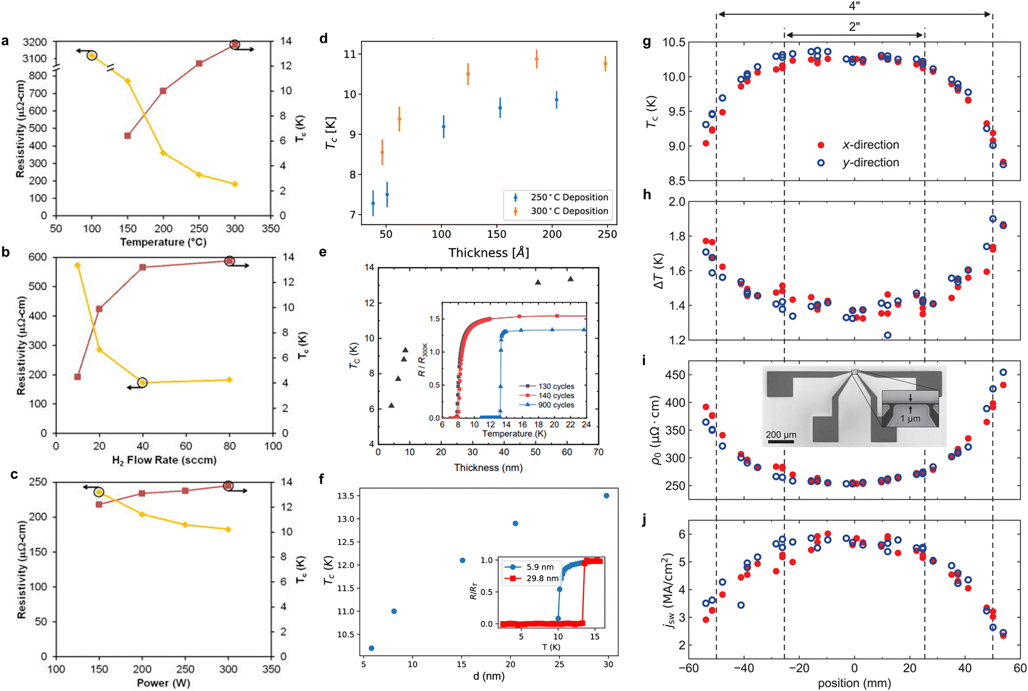 | ||
| Fig. 6 The influences of deposition temperature, H2 flow rate and plasma power on the Tc of NbN films grown by PEALD using TBTDEN and H2/N2 plasma. Room temperature resistivity and Tc as a function of the (a) substrate temperature at 80 sccm H2 and 300 W, (b) H2 flow rate at 300 °C and 300 W, and (c) plasma power at 300 °C and 80 sccm H2.104 Copyright 2017, AIP Publishing. (d) Tc of NbN samples as a function of thickness, with deposition temperature noted.99 Copyright 2020, Springer Publishing. (e) NbN films prepared from TBTDEN and N2/H2 plasma at the substrate temperature of 300 °C and the plasma power of 300 W. Tc of the NbN films vs. the thickness. Inset: Resistance of three NbN films vs. temperature showing the superconducting transition. The resistance is normalized by the room temperature value R300K.102 Copyright 2020, AIP Publishing. (f) Tc versus measured film thickness, d, for thickness series. Inset: Normalised resistance resistance/room temperature resistance ((R/RT))) versus temperature for d = 5.9 nm and d = 29.8 nm films.103 Copyright 2017, IOP Publishing. NbN films deposited by PEALD using TBTDEN as precursor and hydrogen radical for the plasma step with a deposition temperature 380 °C. (g) Distribution of critical temperature, (h) superconducting transition width, (i) residual resistivity at 25 K, and (j) switching current density at 4.2 K over the samples position on the wafer along the x- and y-axis. The measurements were conducted on microbridges of 1 μm width and 6.1 nm thickness (see the scanning electron micrograph in the inset). The vertical dashed lines illustrate wafer edges of the denoted sizes.29 Copyright 2021, AIP Publishing. | ||
For NbN films grown at 300 °C and 300 W plasma power, increasing the H2 flow rate from 10 to 40 sccm resulted in lower resistivity and higher Tc, as shown in Fig. 6(b). However, when the H2 flow was doubled from 40 to 80 sccm, there were slight increases in both resistivity and Tc. Consequently, the lowest resistivity (173 μcm at 40 sccm H2) and the highest Tc (13.7 K at 80 sccm H2) observed in the study did not occur simultaneously, which they attributed to a difference in grain size and oxygen contamination.100,104
The influence of plasma power on room temperature resistivity and Tc was also studied at a constant deposition temperature of 300 °C and H2 flow rate of 80 sccm.104 As shown in Fig. 6(c), increasing plasma power slightly improved both resistivity and Tc. The authors suggested that plasma power might have a more pronounced effect if the deposition temperature and H2 flow rate were further away from their optimal values.104
Sheagren et al.99 studied the influence of deposition temperature (for 250 °C and 300 °C) and film thickness on the Tc of NbN films deposited by PEALD using TBTDEN and Ar-plasma as precursor materials and plasma power of 300 W, see Fig. 6(d). Films grown both at 250 °C and 300 °C exhibited crystalline structure. The Tc increases with both film thickness and deposition temperature. For thinner films around 50 Å, Tc is relatively low, around 7 to 8 K, but it rises as thickness increases, reaching values above 10 K for films thicker than 150 Å. Films deposited at 300 °C generally exhibit higher Tc values compared to those deposited at 250 °C, with the maximum Tc = 10.87 K at 300 °C and around 250 Å thickness. This indicates a strong correlation between thickness, deposition temperature, and the superconducting properties of NbN films. However, the maximum Tc reported in this study is lower than other ALD NbN processes.101,102,104
The superconducting properties of NbN films prepared from TBTDEN and N2/H2 plasma at the substrate temperature of 300 °C, growth rate of 0.68 Å per cycle and the plasma power of 300 W has been reported by Cheng et al.102 The study focuses on the relationship between Tc of the NbN films and their thickness, as illustrated in Fig. 6(e). As anticipated by other researches, a higher Tc is observed for thicker films, reaching a saturation point of 13.3 K at a thickness of 61 nm (900 cycles).102 The inset of Fig. 6(e) provides a closer look at the resistance vs. temperature curves around the superconducting transition region. The remarkably sharp transition observed in the 900-cycles film, with a transition width of only 0.15 K (90% to 10% of resistance), indicates a high level of homogeneity and uniformity in the deposited film.102 In contrast, the 130-cycles and 140-cycles films exhibit a reduced Tc around 8 K and a broader transition width of 1.7 K, suggesting less uniformity in those samples.102
The superconducting properties of NbN films grown from TBTDEN precursor with Ar/H2 plasma with lower deposition temperature of 250 °C is reported by Lennon et al.,103 see Fig. 6(f). As the thickness increases, Tc also rises, nearing a saturation point of 13.5 K for films with a thickness of 29.8 nm. In the ultrathin regime, films exhibit Tc values of 10.2 K for a 5.9 nm thickness and 11.0 K for 8.0 nm. These Tc values are higher to counter reported sputtered NbN films which show Tc values of 8.1 K and 10.3 K for 9 nm films.106 As film thickness decreases, superconducting transition width (ΔTc) increases, indicating reduced uniformity,103 but the PEALD films still show narrower transition widths (0.8 K) compared to sputtered films (1.4 K).106
Knehr et al.29 investigated the wafer-level uniformity of superconducting properties in NbN films deposited via PEALD using the TBTDEN precursor and hydrogen radicals during the plasma step, with a deposition temperature of 380 °C. The uniformity of several superconducting metrics across the NbN film is shown in Fig. 6(e)–(j), revealing minimal variation over a 2-inch diameter wafer. Electrical parameters such as resistivity and critical temperature show only slight deviations near the wafer center. However, as distance from the center increases, especially towards the edges of a 4-inch wafer, a degradation in film quality is observed. At these edges, resistivity increases by an average of 53%, and the switching current density decreases by 45%. The Tc, however, is more stable across the deposition area, showing only a 10% reduction near the edges. They attributed this stability to Tc being determined by contiguous, high-quality regions within the microbridge.29 In contrast, the transition width (ΔTc) provides a better measure of film homogeneity as it reflects the spread of superconducting properties across various regions. Moving from the center to the edge of the 4-inch wafer, ΔTc increases by a notable percentage, indicating reduced homogeneity in different grains and regions of the film. Within the more uniform central region, the Tc aligns with other reports for similar deposition parameters and thicknesses on sapphire substrates.107 However, for other metrics, ALD-NbN films deposited on thermal oxide appear to perform slightly better as superconducting materials, showing a 20% higher switching current density and lower resistivity and transition width by comparable percentages. When compared to slightly thicker ALD-NbN films deposited on SiN, as reported by Cheng et al.,102 the results were similar in most parameters, although Tc was ≈2–3 K higher and the transition width slightly lower (by about 0.3 K).107 The discrepancies could be attributed to differences in deposition temperatures (380 °C vs. 300 °C), plasma gas compositions (pure hydrogen vs. mixed nitrogen/hydrogen), and substrate materials (thermally oxidized silicon vs. LPCVD-grown SiN).102,107
There are only few reports on superconducting NbN films grown by thermal ALD, likely due to their inferior superconducting properties compared to those grown by PEALD. Most efforts in thermal ALD have focused on using NbCl5 and NH3 process chemistry.94,95,97,98 One approach to improve the superconducting properties of thermal ALD NbN films involves introducing Zn vapor between the NbCl5 and NH3 pulses. This technique has been shown to reduce room-temperature resistivity by nearly a factor of two.95,96 Moreover, adding an intermediate Zn pulse increased the Tc of thermal ALD NbN films deposited at 450 °C from 3 K to 5 K.94
4.2.2.1 NbTiN. The binary niobium nitride (NbN) possesses a NaCl-like cubic structure (δ-phase) with a bulk Tc of up to 17.3 K.108 However, this phase exists within a narrow nitrogen content window; outside of this range, other superconducting with lower Tc and non-superconducting phases can form, resulting in films with lower Tc. Additionally, NbN exhibits high normal conducting resistivity and low RRR values due to the presence of vacancies in the lattice.6 In contrast, niobium titanium nitride (NbTiN) retains all the advantages of NbN, particularly the high Tc of 17.8 K,109 while offering significantly lower resistivity and high RRR in the normal state due to the incorporation of Ti atoms into the lattice.6,34,40,110 NbTiN results from the miscible nature of the binary NbN and TiN compounds. Notably, TiN appears to be much less prone to nitrogen off-stoichiometry compared to NbN. Thus, the addition of Ti, which serves as an effective nitrogen getter, stabilizes the δ-phase NbN, resulting in a compound with lower resistivity while maintaining a high critical temperature.6,34,40,110 NbTiN compounds have been deposited using both thermal and plasma enhanced ALD systems. The selected research works from both techniques, focusing on how composition and post deposition treatments can tune the superconducting properties is discussed below.
The superconducting properties of NbTiN films fabricated by PEALD using TBTDEN and TDMAT precursors as Nb and Ti sources and H2/N2-plasma at a deposition temperature 250 °C is reported by Gonzalez et al.40 The Tc and ΔTc of as deposited films as a function of Nb content on NbTiN thin films with eight different compositions is shown in Fig. 7(a). The Tc increases with increasing Nb content in the composition and the maximum Tc of 7 K is reported for Nb0.66Ti0.33N composition, but decreased for the highest Nb concentrations. These findings contradict other studies, where Tc either increases monotonically110 or stabilizes111 for Nb concentrations higher than the ratio 1![[thin space (1/6-em)]](https://www.rsc.org/images/entities/char_2009.gif) :1. The observed lower Tc may stem from the reduced deposition temperature of 250 °C compare to others that exceed 300 °C.34,110 Higher deposition temperatures may induce the growth of denser and more crystalline films leading to higher Tc, whereas a deficit or excess of nitrogen can impact Tc.6 The transition width, remains nearly constant up to the maximum observed Tc, after which it increases slightly but noticeably. Despite this slight increase, all studied concentrations of the ternary compounds exhibit a sharp superconducting transition, with a ΔTc of less than 0.3 K. This narrow transition width is a strong indication of high compositional homogeneity and the excellent quality of the films.40 The Nb0.75Ti0.25N film composition was chosen to investigate the superconducting properties across different film thicknesses, ranging from 6 to 74 nm. The thinnest film does not exhibit a superconducting transition. However, as the thickness increases, the Nb0.75Ti0.25N films become superconducting, with Tc rising and the transition becoming sharper, see Fig. 7(b). Post-deposition annealing was employed to enhance film quality by promoting grain growth, recrystallization, or reducing defects, thereby improving the superconducting critical temperature Tc. Two different thermal treatments were applied to Nb0.75Ti0.25N thin films of varying thicknesses, followed by measurements of their resistance as a function of temperature. From the analysis of the thickest film (74 nm), as shown in Fig. 7(c), two key observations can be made: first, the resistance at low temperatures decreases, and second, Tc shifts to significantly higher values.40 Additionally, the room-temperature resistivity is similar for both rapid thermal annealing (RTA) and slow thermal annealing (STA) at this thickness, which suggests that the STA treatment increases the RRR of the film.40 Notably, the thinnest film (6 nm) becomes superconducting after both annealing procedures, with Tc exceeding 10 K, as seen in Fig. 7(d). This indicates that the as-deposited thinnest film is likely amorphous, and only after thermal treatment it does become polycrystalline, thereby exhibiting superconductivity. In contrast, thicker films (≥10 nm) are already polycrystalline in their as-deposited form and display a superconducting transition. It is important to note that while Tc increases with film thickness after RTA, it stabilizes for films thicker than 25 nm after STA. Overall, both post-deposition thermal treatments significantly improve the properties of the films, with STA yielding a better outcome, achieving a maximum Tc of 15.9 K—the highest value reported to date for both thermal ALD and PEALD techniques. In-plane DC magnetization studies on the thickest Nb0.75Ti0.25N film were performed using a vibrating sample magnetometer (VSM). Fig. 7(e) shows magnetization difference (Δm) vs. magnetic field (H) curves, with the first penetration field Hfp determined for six temperatures (9–14 K). Since Hfp underestimates Hc1, demagnetization effects (N = 0.68) were considered for accurate evaluation. Measurements allowed determination of the Hc1(T) trend for as-deposited and annealed films. Fig. 7(f) presents μ0Hc1 vs. 1 − (T/Tc)2, with μ0Hc1 at 2 K obtained via linear fit: 15 mT for as-deposited, increasing to 81 mT (RTA) and 98 mT (STA),40 aligning with previous reports on PEALD NbTiN films.110,112
:1. The observed lower Tc may stem from the reduced deposition temperature of 250 °C compare to others that exceed 300 °C.34,110 Higher deposition temperatures may induce the growth of denser and more crystalline films leading to higher Tc, whereas a deficit or excess of nitrogen can impact Tc.6 The transition width, remains nearly constant up to the maximum observed Tc, after which it increases slightly but noticeably. Despite this slight increase, all studied concentrations of the ternary compounds exhibit a sharp superconducting transition, with a ΔTc of less than 0.3 K. This narrow transition width is a strong indication of high compositional homogeneity and the excellent quality of the films.40 The Nb0.75Ti0.25N film composition was chosen to investigate the superconducting properties across different film thicknesses, ranging from 6 to 74 nm. The thinnest film does not exhibit a superconducting transition. However, as the thickness increases, the Nb0.75Ti0.25N films become superconducting, with Tc rising and the transition becoming sharper, see Fig. 7(b). Post-deposition annealing was employed to enhance film quality by promoting grain growth, recrystallization, or reducing defects, thereby improving the superconducting critical temperature Tc. Two different thermal treatments were applied to Nb0.75Ti0.25N thin films of varying thicknesses, followed by measurements of their resistance as a function of temperature. From the analysis of the thickest film (74 nm), as shown in Fig. 7(c), two key observations can be made: first, the resistance at low temperatures decreases, and second, Tc shifts to significantly higher values.40 Additionally, the room-temperature resistivity is similar for both rapid thermal annealing (RTA) and slow thermal annealing (STA) at this thickness, which suggests that the STA treatment increases the RRR of the film.40 Notably, the thinnest film (6 nm) becomes superconducting after both annealing procedures, with Tc exceeding 10 K, as seen in Fig. 7(d). This indicates that the as-deposited thinnest film is likely amorphous, and only after thermal treatment it does become polycrystalline, thereby exhibiting superconductivity. In contrast, thicker films (≥10 nm) are already polycrystalline in their as-deposited form and display a superconducting transition. It is important to note that while Tc increases with film thickness after RTA, it stabilizes for films thicker than 25 nm after STA. Overall, both post-deposition thermal treatments significantly improve the properties of the films, with STA yielding a better outcome, achieving a maximum Tc of 15.9 K—the highest value reported to date for both thermal ALD and PEALD techniques. In-plane DC magnetization studies on the thickest Nb0.75Ti0.25N film were performed using a vibrating sample magnetometer (VSM). Fig. 7(e) shows magnetization difference (Δm) vs. magnetic field (H) curves, with the first penetration field Hfp determined for six temperatures (9–14 K). Since Hfp underestimates Hc1, demagnetization effects (N = 0.68) were considered for accurate evaluation. Measurements allowed determination of the Hc1(T) trend for as-deposited and annealed films. Fig. 7(f) presents μ0Hc1 vs. 1 − (T/Tc)2, with μ0Hc1 at 2 K obtained via linear fit: 15 mT for as-deposited, increasing to 81 mT (RTA) and 98 mT (STA),40 aligning with previous reports on PEALD NbTiN films.110,112
 | ||
| Fig. 7 (a) Tc and ΔTc as a function of Nb content on NbTiN thin films with eight different compositions. Solid lines represent a polynomial fit as a guide to the eye. (b) Tc in black and ΔTc in red as a function of Nb0.75Ti0.25N thin film thickness. (c) Resistance as a function of temperature for the thickest Nb0.75Ti0.25N thin film as-deposited (black), and RTA-(red) and STA-treated (blue). (d) Tc as a function of the thickness for as-deposited (black), and RTA-(red) and STA-treated (blue) films. (e) Magnetization curve after subtracting the Meissner line as a function of the applied magnetic field for six different temperatures for the thickest Nb0.75Ti0.25N thin film STA-treated. The red dashed line marks the criterion Δm = 1.810−5 (emu). (f) Δμ0Hc1 vs. 1 − (T/Tc)2 for the thickest Nb0.75Ti0.25N thin-film as-deposited, and RTA- and STA-treated. The linear fit functions are given in the same color-code. The geometrical effect on the evaluation of Hc1 has been taken into account with a demagnetization factor N = 0.68.40 Copyright 2023, AIP Publishing. NbTiN films deposited using thermal ALD with alternating cycles of NbN and TiN using NbCl5, TiCl4 and NH3 precursors at 450 °C. (g) The chemical composition of NbTiN films obtained from XPS analysis as a function of the ALD ratios of NbN and TiN cycles (in red). The dashed line presents the expected composition from the TiN and NbN ratios used in the ALD recipe. (h) Tc of the NbTiN films before and after different annealing treatments measured on sapphire substrates as a function of the Ti content.34,113 Copyright 2023, JACOW Publishing. | ||
Kalboussi et al.34,113 reported the deposition of NbTiN films using thermal ALD with alternating cycles of NbN and TiN, employing NbCl5, TiCl4 and NH3 as precursors at 450 °C. They measured the average titanium and niobium content across the depth profile of the films and analyzed it as a function of the Ti/(Ti + Nb) ratio in the ALD recipe, as shown in their XPS data of Fig. 7(g). The results demonstrated that increasing the number of TiN cycles in the ALD process led to a rise in the Ti/(Ti + Nb) content, following a power-law trend rather than a linear one. Notably, the chemical composition only exceeded a Ti/(Ti + Nb) value of 0.13 when the ALD ratio was above 0.7, consistent with density measurements that showed films with a Ti/(Ti + Nb) ALD ratio below 0.7 had a density similar to pure NbN. To achieve a 25% titanium content, an ALD recipe with 11 TiN cycles and 1 NbN cycle, corresponding to a Ti/(Ti + Nb) ALD ratio of 0.92, was required. They attributed this non-linear behavior to the use of chloride precursors, as films deposited with organometallic precursors like TDMAT and TBTDEN exhibit a linear trend,40 whereas chloride-based precursors suggest that Ti etching occurs during ALD growth.34,113 The as-deposited NbTiN films exhibited low Tc, ranging from 7 to 8 K, significantly lower than the typical 17 K for NbTiN, as summarized in Fig. 7(h). Despite increasing the Ti content, no clear trend in Tc was observed, although resistivity decreased. Structural analysis using XRD and Rutherford Backscattering Spectrometry (RBS) revealed that the films were nitrogen-rich due to the reactions of NbCl5 and TiCl4 with NH3 leading to smaller lattice constants and reduced Tc.34,113 Contrary to the belief that Ti stabilizes the cubic phase of NbN to achieve higher Tc, their ALD-grown films with up to 25% Ti still showed small lattice constants and low Tc values. To address these limitations, they performed post-deposition heat treatments in a vacuum oven, significantly enhancing Tc from 8 K to 15.5 K34,113 and lowering the resistivity of the films, approaching the highest ALD-reported Tc of 15.9 K.40
In an attempt to improve the superconducting response of thermal ALD NbTiN films, zinc (Zn) is added during the growth process, significantly influencing their Tc.31 The incorporation of Zn enhances several key properties of the films, including density and surface roughness, while notably increasing Tc. This effect is particularly pronounced when comparing films with varying Nb/Ti ratios, with an optimal Tc of 12 K achieved at a Nb/Ti ratio of 2, despite TiN being a low-temperature superconductor with a Tc of only <5 K.26,38,77 Interestingly, pure NbN films grown with Zn exhibit a Tc of only 5 K,31 much lower than the expected 16 K for pure NbN. This suggests that Zn indirectly affects Tc by promoting the segregation of impurities, such as hydrogen, with Ti acting as a getter. As the hydrogen content decreases with increasing Ti concentration, Tc improves, doubling from 5 K to 12 K as hydrogen levels drop from 40% to 10%. Therefore, Zn plays a critical role in enhancing the superconducting properties of NbTiN films by improving purity and stabilizing the films structure.31
4.2.2.2 MoCxNy. Molybdenum carbonitride (MoCN) films are attracting significant interest for various applications due to their outstanding electrical conductivity, high thermal and chemical stabilities, superior mechanical strength, and superconductivity.114,115 In the MoCN system, metal atoms form a closely-packed structure with nitrogen and carbon atoms occupying interstitial positions, resulting in several crystalline phases, most of which exhibit superconductivity. Variability in the Tc is influenced by factors such as disorder in crystalline phases and stoichiometric variations, which are intern influenced by films fabrication conditions such as the Mo/(C,N) ratio, deposition temperature, deposition pressure, and deposition method. MoCN films can be fabricated using techniques like CVD, PVD, solid-state reactions, and and ALD.116–118 For films grown by ALD, only one group41 has reported the superconducting behavior of films produced using PEALD.
Bertuch et al.41 reported the synthesis of superconducting molybdenum carbonitride (MoCxNy) films using PE-ALD with the precursor (tBuN)2(NMe2)2Mo and H2/N2-plasma at deposition temperatures between 80 °C and 300 °C. By adjusting these parameters, they controlled the composition and properties of the films. Their study focused on understanding how plasma composition and temperature influenced the chemical structure, as well as the electrical, optical, and superconducting properties of the films, particularly highlighting the correlation between composition and performance. The XPS analysis revealed that the composition of the molybdenum carbonitride films varied significantly based on the nitrogen percentage in the N2/H2 gas mixture and the deposition temperature. Increasing the N2 concentration resulted in a higher proportion of Mo–N bonds and a decrease in Mo–C bonds.41 Conversely, at higher deposition temperatures with a plasma gas mixture of 5.9%N2 in H2, nitrogen incorporation decreased while carbon content increased, suggesting that elevated temperatures enhance carbon ligand removal from the precursor, promoting Mo–C bond formation. Thus, the interplay between plasma composition and deposition temperature significantly influences the films' chemical structure and stoichiometry. The study also examined the electrical and optical properties of the films, such as resistivity, refractive index, and dielectric constant, based on plasma exposure time, nitrogen concentration, and deposition temperature. Films deposited at 150 °C with 11%N2 in H2 exhibited decreased resistivity with longer plasma exposure, indicating enhanced conductivity, as shown in Fig. 8(a). Increasing N2 concentration at this temperature with 40 seconds of plasma exposure at 300 W, also reduced resistivity, likely due to increased Mo–N bond formation, while the refractive index and dielectric constant increased, suggesting denser films Fig. 8(b). Similarly, resistivity decreased with higher deposition temperatures, particularly between 80 °C and 150 °C, stabilizing at elevated temperatures, which also correlated with increases in refractive index and dielectric constant Fig. 8(c). These findings underscore the ability to finely tune the electrical and optical properties of MoCxNy films for advanced electronic and optoelectronic applications. They reported a Tc of 8.8 K for the molybdenum carbonitride film with a composition of MoC0.45N0.08, deposited at 150 °C Fig. 8(d). This value is consistent with the range of Tc values reported for molybdenum carbide deposited using other deposition technique, which typically falls in the range 5.1–12 K.119–121 The superconducting properties were closely linked to the film's composition, particularly the ratio of carbon to nitrogen, and the deposition conditions, emphasizing the importance of precise control over the synthesis process to achieve desired superconducting characteristics.
 | ||
| Fig. 8 Resistivity, refractive index, and dielectric constant of MoCxNy films as a function of (a), the plasma exposure time for 150 °C deposition with 11%N2 in H2. (b) percentage of N2 in H2 with 40 s, 300 W plasma for 150 °C deposition. (c) Deposition temperature with 5.9%N2 in H2, 40 s, 300 W plasma. (d) Superconductivity measurement of 150 °C PE-ALD deposition with 100%H2, 40 s, 300 W plasma.41 Copyright 2017, AIP Publishing. (e) (top) Atomic ratios measured by XPS (closed symbols), with guides to the eye, and EBS (open symbols). (bottom) Lateral grain size (black) and RMS surface roughness (red) of TaCxN1−x films of 19 nm thickness for various applied RF bias powers. (f) Top-view HAADF-STEM images for films prepared with 0 and 20 W RF bias power and cross-sectional HAADF-STEM images for films prepared with 20 and 35 W RF bias power, where the capping layer is prepared by electron beam-induced deposition. The values of film thicknesses, varying between 11 and 35 nm. (g) (top) Critical temperature for the films prepared with 20 W RF bias power for a range of film thicknesses. The inset shows the superconducting transition recorded for the 18 nm film. (bottom) Dependence of the Tc of 19 nm thick films on the RF bias power. At low bias powers, the error bars indicate that no superconducting transition was measured above a temperature of 2.4 K.122 Copyright 2023, AIP Publishing. | ||
4.2.2.3 TaCxN1−x. Tantalum carbonitride (TaCxN1−x) exhibits intriguing superconducting properties that are closely tied to its crystalline structure. Its Tc is governed by its electronic structure, lattice dynamics, and the interplay between its carbon and nitrogen composition.123 The rock-salt cubic structure, typical of this material, creates a high density of electronic states at the Fermi level, which is crucial for the electron–phonon coupling mechanism that drives superconductivity.124 Variations in the x value (carbon to nitrogen ratio) alter the lattice constants and, consequently, the vibrational modes of the crystal lattice, influencing the critical temperature. The superconductivity as a function of chemical composition and lattice parameters for the different TaCN is first reported by Thorwarth et al.123 with Tc varies in the range of 8–12 K. TaCN films are typically fabricated using methods such as PVD, CVD and ALD.122,125–129 While ALD techniques have been extensively used to produce high-quality TaCN films, superconducting properties have been reported by only one research group,122 emphasizing the need for further investigation into this material's superconductivity when synthesized through ALD.
Peeters et al.122 investigated the deposition of superconducting TaCxN1−x thin films using PEALD. The deposition process involved alternating exposures to a tantalum precursor (TBTDMT) and a N2 plasma source, with the use of Ar as a carrier gas. A key factor in controlling film properties was the application of RF bias during the N2 plasma step. The ion energy was controlled via substrate biasing, where a second radio frequency (13.56 MHz) power supply was connected to the substrate table. By varying the biasing power, the voltage over the plasma sheath was adjusted, enhancing the energy of ions impacting the film. Bias powers between 0 W (grounded table) and 35 W were used, resulting in average ion energies ranging from 20 to 250 eV, allowing precise control over ion energy and bombardment on the growing film. This biasing technique enabled adjustments in film composition, grain size, and resistivity, with the deposition temperature held at 250 °C to optimize the superconducting characteristics of the films. The XPS and elastic backscattering spectrometry (EBS) analyses were used to assess the atomic ratios of Ta, C, and N2 in the films, revealing how variations in RF bias power affected stoichiometry throughout the film, see figure Fig. 8(e) (top). Their measurements demonstrated that ion energy during deposition significantly influenced the uniformity and consistency of the films' composition, both on the surface and through the bulk. Increased RF bias power was also associated with larger grain sizes, as confirmed by lateral grain size and surface roughness measurements, leading to improved crystallinity and reduced resistivity without significantly compromising surface smoothness—key for superconducting device integration.122
The group122 also examined the relationship between lateral grain size and RMS surface roughness in the films, as illustrated in Fig. 8(e) (bottom). Their findings indicated that the lateral grain size increases with processing conditions such as higher RF bias power, reflecting enhanced crystallinity and reduced grain boundary density, which contribute to improved electrical properties like lower resistivity. While the RMS surface roughness, shown in red, may increase slightly with grain size due to larger crystalline domains, this increase is modest. This suggests that the films maintain a relatively smooth surface, which is crucial for high-quality interfaces in applications like superconducting quantum devices. Thus, the ability to enhance crystallinity and conductivity without significantly increasing surface roughness is essential for practical device integration. The high-angle annular dark-field scanning transmission electron microscopy (HAADF-STEM) images provide insights into the microstructure of TaCxN1−x films under varying RF bias power, as shown in Fig. 8(f). The film with 0 W RF bias exhibits a fine-grained structure and lower crystallinity, while the 20 W RF bias film shows larger, more defined grains, indicating enhanced grain growth and crystallinity. Cross-sectional images of the 20 W film reveal a uniform and dense structure with well-defined grain boundaries. Increasing the RF bias to 35 W results in even larger grains, suggesting enhanced columnar growth. These results highlight the critical impact of RF bias power on improving the films' crystallinity and grain growth, essential for their electrical and superconducting properties. The Tc of TaCxN1−x films prepared with 20 W RF bias across various thicknesses is shown in Fig. 8(g) (top). The Tc remains stable around 7 K, indicating that the superconducting properties are well-maintained regardless of thickness. The inset reveals a sharp drop in resistivity to zero for an 18 nm thick film, confirming its superconducting behavior and suggesting high film quality with minimal defects.122
The influence of RF bias power on Tc was also examined in 19 nm thick samples, as depicted in Fig. 8(g) (bottom). The groups findings revealed a significant increase in Tc with higher RF bias power. At low bias powers, the lack of measurable superconducting transitions above 2.4 K indicates insufficient superconducting properties, likely due to poorer crystallinity or higher impurity levels. However, as RF bias power rises, Tc approaches 7 K, highlighting the critical role of RF bias in enhancing superconducting properties through improved film quality, increased grain size, and reduced impurities. The enhanced ion energy from higher RF bias likely facilitates a more homogeneous and well-ordered film structure conducive to superconductivity.
4.2.3.1 NbC. Niobium carbide (NbC) has attracted considerable research attention due to its unique combination of high chemical stability, high thermal stability, low electrical resistance and superconductivity.130,131 Stoichiometric NbC crystallizes in a rock-salt structure, where niobium atoms form a cubic lattice, and carbon atoms occupy the octahedral interstitial sites.131 NbC can be synthesized using various techniques, such as Pulsed laser ablation,132 CVD,133 sputtering134 and ALD,32 with only one group reported the superconducting properties of ALD grown NbC films.32 A study by Klug et al.32 examines the synthesis of these films through ALD using TMA, NbF5, and NbCl5 as precursors, within a deposition temperature range of 125–350 °C.
To ensure the purity of the grown films, the authors32 conducted XPS and RBS measurements, revealing varying amounts of impurities, including amorphous carbon(a-C), AlF3, NbFx, and NbClx, were found in all samples, see Fig. 9(a) and (b). Films synthesized from TMA and NbF5 contained Al, C, F, Nb, and O, with concentrations varying by deposition temperature. XPS analysis showed a decrease in Al (6 to 2 atom%) and F (55 to 6 atom%) concentrations as the temperature increased from 125 °C to 350 °C, while C (20 to 44 atom%) and Nb (15 to 28 atom%) increased. Oxygen peaked at 27 atom% at 300 °C, then dropped to 20 atom% at 350 °C. RBS detected no oxygen at 150 °C or 350 °C, suggesting that the oxygen observed by XPS resulted from surface oxidation post-deposition. Both XPS and RBS showed similar trends for Al, C, F, and Nb concentrations, and adjusting XPS for surface oxides provided results comparable to RBS, with the corrected composition at 350 °C being 2.4 atom% Al, 61–63 atom% C, 8.3–8.6 atom% F, and 26–28 atom% Nb. Additionally, XPS analysis across the 125 °C to 350 °C temperature range indicated that niobium was primarily in the Nb–C bonding state, characteristic of niobium carbide, with fluorine attributed to the use of NbF5 as precursor. Despite variations in fluorine content, the stoichiometry of niobium carbide remained consistent, suggesting that fluorine did not significantly disrupt the formation of the desired carbide phase.32
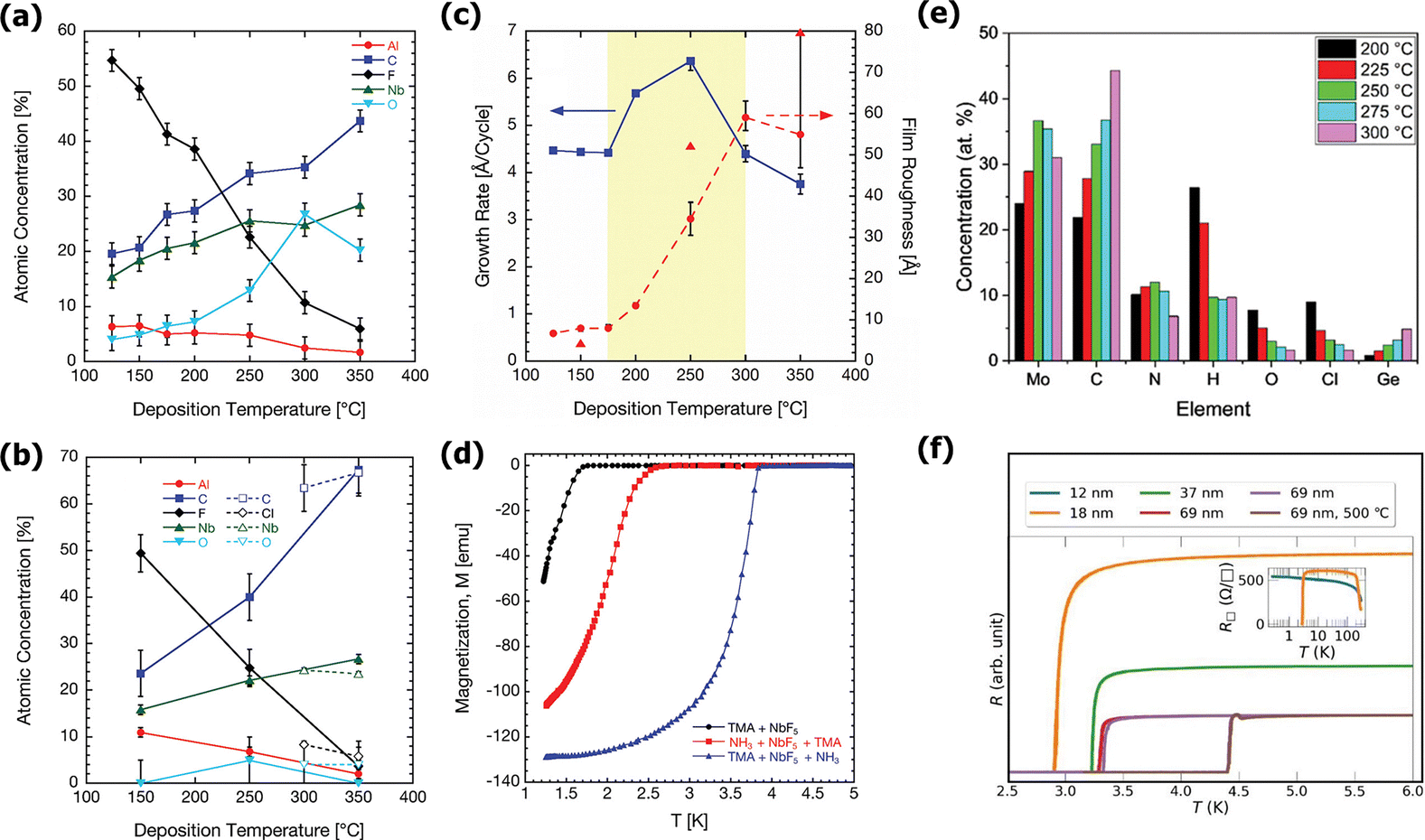 | ||
| Fig. 9 NbC film composition measured by (a) XPS and (b) RBS vs. deposition temperature between 125 and 350 °C. XPS spectra were acquired following a 5–10 min Ar ion-milling step to remove surface contamination. Data from films grown with NbF5 and NbCl5 are represented by filled and open shapes, respectively. (c) The film growth rate determined by XRR (squares) and roughness determined by XRR (circles) and AFM (triangles) as a function of deposition temperature. (d) SQUID measurements of superconducting critical temperature Tc for films grown on Si(001) with the precursor sequence TMA + NbF5 (circles), NH3 + NbF5 + TMA (squares), and TMA + NbF5 + NH3 (triangles).32 Copyright 2011, ACS Publishing. (e) ToF-ERDA compositional analysis of MoCx films deposited at various temperatures (f) resistance of six MoCx samples as functions of temperature. The red and violet lines show measurements of two nominally similar 69 nm samples cleaved from the same larger chip. The brown line shows the measurement of a third sample cleaved from the same 69 nm chip, which was annealed at 500 °C before the cryogenic measurement. The inset shows the absolute sheet resistances of 12 nm and 18 nm films, deposited on non-conductive substrates, as a function of temperature up to 300 K. The orange line is from the same measurement as in the main panel.36 Copyright 2024, Wiley Online Library Publishing. | ||
The authors32 investigated the effect of deposition temperature on film growth rate and surface roughness using XRR and AFM (Fig. 9c). The growth rate, as determined by XRR, remained constant (4.5 Å per cycle) up to 175 °C, increased to 6.3 Å per cycle at 250 °C, and decreased to 3.8 Å per cycle at 350 °C. This nonmonotonic trend was attributed to possible temperature-dependent changes in surface species or active site density. Surface roughness, determined by XRR, stayed below 0.8 nm below 175 °C but increased significantly above 175 °C, from 1.3 nm at 200 °C to 5.9 nm at 300 °C. Due to XRR's limitations with Gaussian roughness assumptions, AFM was used for validation, showing roughness values of 0.4 nm at 150 °C, 5.2 nm at 250 °C, and 8.0 nm at 350 °C.32
The superconducting properties of films grown with NbF5 measured by SQUID are shown in Fig. 9(d). Only films deposited at temperatures of 350 °C or higher displayed a superconducting transition above 1.2 K, with the maximum transition temperature recorded at Tc = 1.8 K (represented by circles) for a 75 nm thick film grown at 350 °C using 200 cycles of TMA and NbF5 on Si(001). This Tc is notably lower than that of bulk NbC, which has a Tc of 12 K,130 largely due to a high level of impurities present in the films. However, the introduction of NH3 into the ALD process significantly improved the superconducting characteristics. When the sequence was modified to NH3 + NbF5 + TMA (squares), the Tc increased significantly to 2.5 K. Further enhancement of the Tc was achieved with the sequence TMA + NbF5 + NH3 (triangles), resulting in a Tc of 3.8 K. The enhanced transition temperatures in films grown with NH3 can be attributed to a reduced fluorine content from the reducing agent.32 These measurements indicate that the introduction and positioning of NH3 in the precursor sequence can effectively tune the superconducting properties of the films.
4.2.3.2 MoC. Molybdenum carbide (MoC) thin films exhibit superconductivity with Tc in the range of 2.8–14.7 K.36,41,135–138 They have been deposited by both physical and chemical deposition methods, including PVD,139 carburization,140 CVD,141 and ALD.36,41,142,143 Recent research by Kärkkäinen et al.36 has delved into the superconducting properties of molybdenum carbide thin films (MoCl5) synthesized through ALD by utilizing MoCl5 as the metal precursor and (Me3Ge)2DHP as the carbon source. The ALD process was conducted at temperatures between 200 and 300 °C, achieving a growth rate of 1.5 Å per cycle. This resulted in smooth films with a root mean square (RMS) roughness ranging from 0.3 to 0.6 nm across various substrates, including Si, TiN, and HfO2. Notably, film growth was continuous even after just five cycles.36
Compositional analysis of the MoCx films, as measured by Time-of-Flight Elastic Recoil Detection Analysis (ToF-ERDA), indicated that carbon content varied with deposition temperature, see Fig. 9(e). Lower deposition temperatures favored carbon incorporation from the precursor, while higher temperatures reduced carbon content due to enhanced desorption of volatile species and more efficient Mo–C bond formation. Chlorine contamination, a residual from the precursor, also decreased with increasing deposition temperature, indicating more complete reactions, while minimal oxygen presence suggested low oxidation levels, preserving the films' electrical and structural integrity. Cryogenic measurements of molybdenum carbide films of various thicknesses (12,18,37, and 69 nm) deposited at 275 °C revealed superconductivity as shown in Fig. 9(f). Two samples from a 69 nm film exhibited consistent Tc values of approximately 3.3 K, while a 37 nm sample showed Tc of about 3.2 K and an 18 nm film had Tc of 2.9 K.36 Annealing a third chip from the same 69 nm film at 500 °C under nitrogen increased Tc to 4.4 K, suggesting that annealing can enhance superconducting properties by improving micro-structure. However, attempts to anneal the 69 nm films at 650 °C resulted in peeling and they argued it as an indication for compromised adhesion or structural integrity at higher temperatures. For the 12 nm and 18 nm films on non-conductive substrates, the inset of the data of Fig. 9(f) showed that both exhibited increasing resistivity as the temperature decreased, with a RRR of less than 1, typical for disordered metals. The 12 nm film remained resistive down to 0.3 K, indicating it did not transition to a superconducting state within the measured range.36 These results highlight the influence of film thickness and annealing on superconducting properties, with thicker and annealed films demonstrating better superconductivity.
Moreover, various molybdenum carbide materials, prepared using different techniques aside from ALD, exhibit superconducting properties, with their Tc depending on their crystal structure and synthesis methods. The cubic δ-MoC0.681, synthesized from stoichiometric carbon and Mo powder under high pressure (6 GPa), features numerous disordered carbon vacancies and has a Tc of 12 K.119 In contrast, the hexagonal-layered η-Mo3C2, fabricated from powders pressed at 1700 °C under 6 GPa, shows a Tc of 8.5 K.120 Molybdenum carbide films, particularly in the α-Mo2C and β-Mo2C phases, demonstrate superconductivity with Tc values ranging from 5.1 to 8.9 K.121 Notably, the highest reported Tc for molybdenum carbide is 14.7 K, observed in a single-cubic δ-MoC1−x film, synthesized via arc melting solidification with a composition between MoC0.65 and MoC0.75.138 While molybdenum carbide thin films deposited by ALD exhibit lower Tc values, their superconducting properties are promising and can be finely tuned through controlled deposition and post-deposition treatments, potentially matching or even surpassing currently reported best values.
4.2.4.1 NbSi. Niobium and silicon are known to form bulk binary intermetallic niobium silicides that exhibit a range of stable compositions.144,145 From these compositions different polymorphs of Nb3Si and NbSi exhibited superconductivity.144,146,147 NbxSi1−x films with various compositions can be deposited using a variety of methods including electron beam powder bed fusion,148 sputtering,149 CVD,150 and ALD.146
Proslier et al.146 demonstrated a successful synthesis of superconducting NbSi films with 1:1 stoichiometry using ALD. The researchers used niobium pentafluoride (NbF5) and disilane (Si2H6) as precursors, conducting experiments at various temperatures (150–400 °C) to explore the effects on film growth, structure, and superconductivity. The cross-sectional SEM images of NbSi films deposited on silicon trench structures at 200 °C using 300 NbSi cycles revealed that the films are highly uniform, conformal, and pinhole-free, showing the effectiveness of the ALD process in achieving excellent coverage, even on complex 3D structures, see Fig. 10(a).146
 | ||
| Fig. 10 (a) SEM image of a NbSi film grown on trenched Si(100) wafer at 200 °C using timing sequence 2-10-1-10 and 300 ALD cycles. (b) Composition of NbSi films measured by RBS and (c) binding energy of the Nb and Si peaks as a function of the growth temperature of films grown on Si(100) with 100 cycles using the same timing sequence. (d) Resistance versus temperature of a NbSi films grown at 200 °C on Si(100). The insert is an expanded view near the superconducting transition, indicated by a dashed line. (e) SQUID magnetometry measurements on NbSi films grown on Si(100) using the same timing sequence. The curves labeled “as grown” correspond to measurements done on as grown films, and the dashed lines correspond to measurement done after a postannealed films in Ar and the dotted lines in N2. The postannealing temperatures 400 or 600 °C are shown next to the corresponding curves.146 Copyright 2011, ACS Publishing. (f) SEM images of 3D structures, called stacks, in the left top view of the stack; in the right, the CuO film inside 3D substrate (stack) are shown. (g) X-ray diffraction patterns of CuO thin films grown on SiO2/Si substrate by using different number of deposition cycles indicated by labels. (h) Electrical resistivity of CuO film grown after 5000 ALD cycles, with the thickness of 94 nm. The inset shows the low-temperature region.35 Copyright 2020, MDPI Publishing. | ||
Proslier et al.146 utilized RBS measurements to assess the composition of the NbSi films, revealing that for all studied temperatures, the films consistently maintained an Nb:Si ratio of 1:1 across the sample area with no detectable fluorine impurities, see Fig. 10(b). This uniform composition was observed even at deposition temperatures above 275 °C, where usually the growth shift towards CVD behavior. The researchers attributed this consistency to a stable growth mechanism involving silicon deposition during Si2H6 exposure and partial silicon etching during NbF5 exposure. In addition to RBS measurements, XPS analysis showed that the binding energies of the niobium and silicon peaks remained stable across different growth temperatures, see Fig. 10(c). This confirmed that the chemical composition and bonding were preserved throughout the deposition process, ensuring reliable film properties. The temperature dependence of the resistance between 2 and 50 K, measured on a NbSi film grown on a Si(100) substrate using 100 ALD cycles at 200 °C, is shown in Fig. 10(d). The graph exhibits a sharp decrease in resistance below the critical temperature Tc = 3.1 K, indicating a superconducting transition. This marked the first instance of a superconducting NbSi film with a 1:1 stoichiometry, a significant milestone in the field.146 Fig. 10(e) represents the sample magnetization M, as measured by SQUID, under an external magnetic field of 10 mG applied perpendicular to the sample as a function of the temperature. Fig. 10 (e:top) shows SQUID measurements of a multilayer structure grown at 200 °C, indicating a broad superconducting transition below 3.1 K, consistent with the maximum Tc measured by resistivity. They attributed the broad Tc distribution to the possible compositional inhomogeneities, although RBS indicated a uniform 1:1 NbSi ratio. Hydrogen trapped in the films may also cause broad transitions, as hydrogen is known to affect superconductivity. In contrast, a sharper transition was observed for NbSi films grown at 400 °C in the CVD regime. Similar results were seen in films grown at 225 °C and 275 °C, see Fig. 10 (e: middle and bottom). Annealing the samples at 400 °C in Ar or N2 atmospheres significantly sharpened the transitions, suggesting hydrogen diffusion out of the films improved superconducting homogeneity.146 NbSi films grown at 200 °C and capped with ALD Al2O3 were further annealed at 600 °C. Post-treatment, XPS detected oxygen in the films, and SQUID measurements showed a suppressed Tc down to 2 K, see Fig. 10 (e: top). Films grown at 225 °C and 275 °C became insulating and changed color after the same treatment, possibly due to nitrogen incorporation forming a silicon/niobium nitride alloy.146
4.2.4.2 CuO. Tamm et al.35 reported the synthesis and characterization of the first superconducting cupric oxide (CuO) thin films using ALD on both planar and three-dimensional substrates. The study aimed to optimize the ALD process for CuO films and assess their superconducting properties at low temperatures. Copper(II)-bis-(dimethylamino-2-propoxide) [Cu(dmap)2] and ozone were used as precursors, with ALD cycles ranging from 500 to 10
000. Film growth occurred within a temperature range of 112 °C to 165 °C, with 140 °C identified as the optimal temperature for high-purity film deposition.The grazing incidence X-ray diffraction (GIXRD) patterns of CuO thin films grown at 140 °C using varying numbers of ALD cycles is shown in Fig. 10(g). The XRD data reveal that the films crystallized predominantly in the CuO phase, as indicated by the diffraction peaks corresponding to CuO. The intensity of the peaks increases with the number of deposition cycles, reflecting the growth in film thickness and improved crystallinity as the deposition progresses.35 The influence of the number of cycles on the morphology of CuO films grown on both 2D and 3D structures is illustrated in Fig. 10f). Notably, even with a large number of cycles, the films exhibit significant coverage on three-dimensional substrates with an aspect ratio of 1:20. Unlike planar Si(111) substrates, these 3D substrates have etched vertical channels perpendicular to the surface. Achieving adequate coverage is essential for effectively coating arbitrarily shaped nanostructures with functional films, particularly for applications in quantum-computer-related technologies. Electrical resistivity measurements were carried out using the two-probe method at low temperatures ranging from 1.8 K to 300 K, see Fig. 10(h). At room temperature, the CuO films demonstrated a resistivity of approximately 0.55 Ω cm, with a slight temperature dependence in the 10–300 K range. However, a significant resistivity drop was observed at around 4 K, where the resistivity fell by 50%, reaching about 0.27 Ω cm at 2 K. This abrupt change may suggest the emergence of low-temperature superconductivity in the CuO films. However, they remark the need of further investigation to confirm this phenomenon and rule out other potential causes, such as film shrinkage or thermal expansion mismatches.35
La2−xSrxCuO4−y. Sønsteby et al.42 conducted a pioneering study that demonstrated the successful deposition of the first complex oxide thin film with superconducting properties using ALD. Their research focused on the deposition of the compound La2−xSrxCuO4−y (LSCO), a complex cuprate oxide with a layered perovskite structure. LSCO has attracted attention for its superconducting properties, making it a valuable material for applications in advanced electronic systems. The study aimed to control the stoichiometry and structural properties of the LSCO films, investigating how these factors influence superconductivity. They successfully deposited LSCO thin films using the ALD process with La(thd)3 and Cu(acac)2 precursors and ozone. The films were grown at a temperature of 250 °C on LaAlO3 (LAO) substrates, chosen for their structural compatibility with LSCOs layered perovskite structure. The researchers carefully controlled the stoichiometry of the films by adjusting the ratios of La, Sr, and Cu precursor pulses. Initially, the films were amorphous, but post-deposition annealing at temperatures between 400 °C and 1000 °C induced crystallization. XRD analysis revealed that crystallization occurred at 650 °C into the Ruddlesden–Popper (RP) phase, essential for achieving LSCO's superconducting properties. This precise control over the deposition parameters was critical in producing the desired superconducting behavior in the LSCO films.
The study42 utilized X-ray fluorescence (XRF) to measure the cation percentage of strontium (Sr) in the LSCO films as a function of the Sr precursor pulse ratio during ALD, see Fig. 11(a). The results indicated that the actual Sr content in the films did not increase linearly with the pulse ratio and was lower than expected at higher pulse percentages, suggesting non-ideal uptake or saturation effects. This finding highlights the complexity of achieving precise dopant control in ALD processes and emphasized the need for careful calibration to obtain the desired stoichiometry in complex oxide films. To verify the epitaxial growth and orientation of the LSCO films, cross-sectional STEM was employed, see Fig. 11(b). The analysis confirmed a high degree of epitaxial alignment between the LSCO films and the LAO substrate, with the crystalline planes of the film aligning well with those of the substrate. This structural coherence is critical for the superconducting properties observed in the study. Furthermore, the specific resistivity of the LSCO films was examined as a function of Sr content, see Fig. 11(c). It was found that the resistivity is highly dependent on the Sr doping level. Films with lower Sr concentrations exhibited insulating behavior with higher resistivity, while an increase in Sr content to ≈5–6% resulted in a decrease in resistivity, indicating a transition to metallic behavior. Notably, near the composition La1.8Sr0.15CuO4−y, the resistivity dropped sharply at low temperatures, signaling the onset of superconductivity. In addition, the specific resistivity of a 40 nm La1.81Sr0.19CuO4−y thin film was measured, revealing metallic behavior at higher temperatures, with resistivity decreasing as temperature decreased, see Fig. 11(d). A sharp transition occurred around 20 K, where the resistivity dropped to near zero, indicating the onset of superconductivity with a Tc of approximately 20 K. However, this Tc is lower than that observed in bulk cuprate systems with x = 0.15, which exhibit higher Tc values around 40 K.151
 | ||
| Fig. 11 (a) Cation percentage of Sr in the deposited film measured by X-ray fluorescence as a function of the cation percentage of strontium pulses in the process. The orange dotted line represents a theoretically linear response, while the black line corresponds to the observed response. (b) Cross-section HAADF-STEM image of La1.8Sr0.15CuO4−y on a LaAlO3(100) substrate. (c) Specific resistivity as a function of Sr content in the films. All data was collected for a sample annealed at 700 °C for 15 minutes in air. (d), Specific resistivity as a function of temperature for a 40 nm La1.81Sr0.19CuO4−y thin film deposited on LAO(100). The dotted blue line indicates the temperature where the resistivity starts to drop.42 Copyright 2018, Royal Society of Chemistry Publishing. | ||
While ALD LSCO thin films have demonstrated superconducting properties with a maximum Tc of 20 K, this relatively low Tc presents a significant barrier to widespread practical applications, especially when compared to high-Tc superconductors such as YBCO (Tc ≈ 93 K)152 and iron-based superconductors Tc ≈ 55 K.153 The low Tc limits the efficiency and applicability of LSCO films in technologies where higher operating temperatures are desirable. In addition to this limitation, challenges such as achieving optimal stoichiometry and phase purity during and after deposition, as well as the inherent material properties, further hinder performance at higher temperatures and restrict broader applications. To address these challenges, strategies such as optimizing ALD process parameters (e.g., adjusting precursor selection and deposition temperature), introducing chemical dopants (e.g., Ba, Ca, Li, and Mg154,155) to modify the electronic structure, and applying strain engineering through substrate selection can help improve Tc. Additionally, constructing layered heterostructures, implementing post-deposition annealing to control oxygen content, and exploring nanostructuring techniques can further enhance the Tc, providing potential pathways to improve material performance and expand its practical applications. These strategies are not only applicable to LSCO but also hold potential for other superconducting complex oxides that can be synthesized via ALD.
4.3 Summary
The quest for higher-quality superconducting thin films characterized by fewer defects, greater uniformity, and enhanced homogeneity remains a fundamental goal in thin film preparation. ALD plays a crucial role in achieving these qualities, as it offers precise control over film thickness, composition, and uniformity factors critical for optimizing the superconducting transition temperature (Tc). Moreover, higher deposition temperatures during ALD generally lead to improved film crystallinity, reduced impurity incorporation, and enhanced surface smoothness, all of which contribute to superior superconducting properties. In addition, post-annealing treatments can further refine the films microstructure, relieve residual stress, and enhance phase purity, leading to improved electrical transport properties and a potential increase in Tc. ALDs atomic-level precision, combined with optimized deposition temperatures and post-deposition annealing, ensures uniformity across large areas and makes it an indispensable technique for advancing superconducting thin film technology.Furthermore, ALD particularly through the use of supercycle approaches, has enabled the fabrication of complex, multicomponent superconductors such as LSCO and NbTiN. These supercycling techniques facilitate precise control over composition and thickness, making them especially well-suited for engineering layered heterostructures or nanolaminates with tailored superconducting properties. For instance, non-superconducting AlN layers deposited in vacuum by PEALD have been used as a buffer or interface layer for the epitaxial growth of NbTiN on silicon substrates, improving crystallinity and performance.40 Moreover, ALD has been employed to create protective capping layers—offering conformal coverage and oxidation resistance for air-sensitive superconducting materials.156 The capability of ALD to deposit uniform, pinhole-free layers on complex 3D topographies makes it a uniquely advantageous technique for constructing superconducting heterostructures, interface engineering, and protective layering, often beyond the capabilities of traditional methods such as sputtering or PLD.
Table 3 summarizes various ALD processes for producing superconducting thin films, detailing various materials, precursors, substrates, deposition temperatures, and resulting Tc. It showcases a diverse range of materials, including TiN, NbTiN, and complex oxides like La2−xSrxCuO4−y. Deposition conditions vary significantly, with temperatures ranging from 80 °C to 500 °C and GPC values from 0.1 to 4.5 Å. The highest Tc reported is 20 K for La2−xSrxCuO4−y. The table also highlights the impact of different precursors and substrates on the quality and properties of the deposited films, as well as the need for specific crystallization conditions to attain optimal superconducting performance.
| Material | Atomic layer deposition | Cryst. req. | Tc (K) | Ref. | ||||
|---|---|---|---|---|---|---|---|---|
| Precursors | Substrate | Dep. temp. /(°C) | GPC/(Å) | |||||
| Precursor A | Precursor B | |||||||
| Si = silicon, BSG = borosilicate glass, QZ = quartz, FS = fused silica, Sa = sapphire. SG = soda glass, Nb = niobium, As-dep. = As deposited, vac. = vacuum. | ||||||||
| TiN | TiCl4 | NH3 | Si | 450 | 0.24 | As-dep. | 3.4 | 5 |
| TiN | TiCl4 | NH3 | Si | 350–450 | 0.23–0.33 | As-dep. | 3.8 | 26 |
| TiN | TiCl4 | N2/H2-plasma | Si | 400 | 0.45 | As-dep. | 3.6 | 27 |
| TiN | TDMAT | N2/H2-plasma | Si | 350 | As-dep. | 2.09 | 157 | |
| TiN | TDMAT | N2/Ar-plasma | Si | 300 | 0.65 | As-dep. | 4.35 | 77 |
| TiN | TDMAT | N2-plasma | Si | 270 | 0.9 | As-dep. | 4.62 | 38 |
| NbN | NbCl5 | NH3 | SG | 500 | — | As-dep. | ≈10 | 30 |
| NbN | NbCl5 | NH3 + Zn | SG | 450 | 0.2 | As-dep. | 5 | 31 |
| NbN | TBTDEN | Ar-plasma | Si | 250–300 | 0.51–0.62 | As-dep. | 10.9 | 99 |
| NbN | TBTDEN | H2-plasma | Si | 350 | 0.46 | As-dep. | 13.8 | 101 |
| NbN | TBTDEN | H2/Ar-plasma | Si | 250 | 0.12 | As-dep. | 13.5 | 103 |
| NbN | TBTDEN | H2/N2-plasma | Si | 100–300 | 0.35–0.76 | As-dep. | 13.7 | 104 |
| NbN | TBTDEN | H2/NH3-plasma | Si | 350 | 0.55 ± 0.02 | As-dep. | 12.3 | 105 |
| NbN | TBTDEN | H2/NH3-plasma | Si | 240–400 | 0.1–0.25 | 1000-Ar | 13.8 | 39 |
| NbTiN | NbF5,TiCl4 | NH3 + Zn | Sa | 450 | As-dep. | 13.4 | 33 | |
| NbTiN | NbCl5,TiCl4 | NH3 | Nb, Sa | 450 | 0.24 ± 0.03 | 850-vac. | 15.5 | 34 |
| NbTiN | TBTDEN, TDMAT | H2/N2-plasma | Si | 250 | 0.62 | 1000-vac. | 15.9 | 40 |
| NbC | NbF5 | TMA | Si, FS | 350 | 3.75 | As-dep. | 1.8 | 32 |
| NbC | NbF5 | TMA + NH3 | Si, FS | 350 | 3.75 | As-dep. | 3.8 | 32 |
| NbSi | NbF5 | Si2H6,SiH4 | Si, Sa | 150–400 | 4.5 | As-dep. | 3.1 | 146 |
| CuO | Cu(dmap)2 | O3 | Si | 112–165 | 0.16–0.39 | As-dep. | 4 | 35 |
| MoN | MoCl5 | NH3 | BSG | 450 | 0.31 ± 0.02 | As-dep. | 11.3 ± 0.05 | 33 |
| MoCx | MoCl5 | (Me3Ge)2DHP | Si,TiN, HfO2 | 200–300 | 0.36–0.56 | As-dep. | 2.9–4.4 | 36 |
| MoC0.4_5N_0.8 | (tBuN)2(NMe2)2Mo | H2/N2-plasma | Si | 80–300 | 0.36–0.56 | As-dep | 8.8 | 41 |
| TaCxN1−x | TBTDMT | Ar/N2-plasma | Si | 250 | 0.35–0.55 | 7 | 122 | |
| La2−xSrxCuO4−y | La(thd)3, Cu(acac)2 | O3 | Si | 250 | 0.35–0.55 | 700-air | 20 | 42 |
Fig. 12 summarize the highest reported Tc of various thin films deposited by ALD. The different materials deposited by ALD exhibit a wide range of Tc values, from approximately 1.8 K to 20 K. The highest Tc is observed for La2−xSrxCuO4−y films, while other materials like NbN and NbTiN also show relatively high Tc values. The diversity in Tc values reflects the influence of material choice and deposition conditions on the superconducting properties of thin films produced via ALD.
 | ||
| Fig. 12 The Tc of different superconducting thin films deposited by ALD. The Tc are the highest values reported for each processing conditions and the processing conditions are summarized in Table 3. | ||
5 Applications
5.1 Multipacting mitigation for SRF cavities
Multipacting is a phenomenon that occurs in superconducting radio frequency (SRF) cavities where secondary electron emission causes an avalanche of electrons, leading to resonant electron buildup.16,158,159 This can severely degrade the performance of SRF cavities by increasing power losses, creating local heating, and potentially damaging the cavity surfaces.16,158,159 Mitigating multipacting is crucial for enhancing the efficiency and longevity of SRF cavities, which are vital components in particle accelerators. Beyond SRF cavities, multipacting also affects a variety of RF devices, such as divertors in tokamaks,160 satellite systems,161 power couplers,162 and antennas, emphasizing its widespread impact on RF technologies.163Recent study by Kalboussi et al.164 have explored the role of ALD in mitigating multipacting by optimizing the properties of superconducting thin TiN coatings. They explored how the thickness of ALD-grown TiN films influences the total electron emission yield (TEEY), chemical composition, and resistivity. To test their approach for mitigating multipacting, they initially deposited a 10 nm layer of Al2O3 inside a 1.3 GHz cavity, followed by post-annealing at 650 °C for 10 hours in high vacuum conditions (approximately 10−6 mbar). This procedure was intended to reduce two-level system dissipations in 3D superconducting niobium resonators.163 The experiment was repeated twice on the same cavity, with surface resets achieved through chemical etching between Al2O3 depositions and annealing cycles. Both RF tests conducted after deposition and post-annealing showed a strong, reproducible multipacting barrier between 15 and 18 MV m−1, which could not be processed further, preventing higher accelerating fields from being reached, see Fig. 13. A baseline RF test performed before the ALD deposition achieved a maximum accelerating field (Eacc) of 32 MV m−1.164
 | ||
| Fig. 13 RF tests at 1.45 K of an ALD coated 1.3 GHz Nb cavity with different surface treatments. The green curve, baseline measurement, blue RF tests after 10 nm coatings of Al2O3 and post-annealed at 650 °C in high vacuum, and red with additonal 1.6 nm TiN film + annealing113,164 Copyright 2024, AIP Publishing. | ||
The significant multipacting barrier observed was attributed to the three orders of magnitude higher electron emission from the Al2O3 surface compared to the bare niobium surface, with a TEEYMAX of 4.6 for Al2O3 compared to 2.3 for niobium. To address this issue, they applied two different TiN film thicknesses 5 nm and 1.6 nm on top of a 10 nm Al2O3 layer. The RF tests conducted after applying the 5 nm TiN coating revealed a significant degradation in the quality factors (Q0), with values dropping by over two orders of magnitude to 108, and a corresponding increase in surface resistance to 2200 nΩ.164 Subsequent RF testing with a thinner 1.6 nm TiN coating showed a substantial improvement. The quality factor increased to the range of 1010, see Fig. 13. Additionally, the surface resistance decreased from 2200 nΩ to 10.8 nΩ at low temperatures upon reducing the TiN thickness. Notably, the multipacting barrier at 18 MV m−1 disappeared, enabling the accelerating gradient to extend from 18 MV m−1 to 35 MV m−1, effectively restoring the performance of the cavity to its baseline levels achieved with bare niobium.
5.2 Superconducting electronics and quantum devices
SNSPDs are typically fabricated as narrow nanowires, ranging from 20 nm to 150 nm in width, using ultrathin superconducting films between 3 nm and 10 nm thick. Two main classes of materials are used in their construction: polycrystalline nitride superconductors, like NbN171 and NbTiN,173 known for their high critical temperatures and fast response times, and amorphous alloy superconductors, such as WSi,166 MoSi,174 and MoGe,175 valued for their high internal efficiencies and uniform structure. The choice of material depends on specific application needs, with polycrystalline nitrides offering higher critical currents and faster detection capabilities, while amorphous alloys provide superior photon detection efficiency and are ideal for large-area detector arrays.
In their paper, Cheng et al.102 present a detailed study on the fabrication and characterization of superconducting SNSPDs using PEALD NbN films. The fabricated detectors demonstrate broad saturated plateaus in the efficiency curves that are comparable with amorphous detectors, while simultaneously maintaining high switching currents. The authors fabricate 450 SNSPDs on each NbN chip, with nanowires of 50 nm, 75 nm, and 100 nm widths. These nanowires are patterned into circular shapes with a 15 μm diameter for the active detection area, surrounded by floating nanowires for proximity effect correction during electron-beam exposure, forming a larger 25 μm diameter circle, see Fig. 14(a) and (b). SEM reveals that the 50 nm-width nanowires exhibit exceptional uniformity, with less than 5 nm variation across the detection area, see Fig. 14(c). TEM provides cross-sectional images showing a nanowire thickness of 9.5 nm, including a 2 nm native oxide layer, further emphasizing the precision and quality of the 140-cycle NbN films used in fabrication, see Fig. 14(d). Fig. 14(e) presents a compelling plot of normalized photon counts as a function of the relative bias current (Ibias/ISW) for SNSPDs with varying widths (100 nm, 75 nm, and 50 nm). The results showcase the intrinsic switching current ISW for each detector type, illustrating the relationship between bias current and photon detection efficiency. The broad saturation plateaus observed in the photon counting curves indicate high internal efficiencies across the different designs, which is a crucial characteristic for the practical application of SNSPDs. The green dashed lines denoted the saturation current (Isat), reinforcing the importance of operating above this threshold to achieve optimal performance. As can be seen in Fig. 14(e) the detectors fabricated from the 140-cycle NbN films (with a thickness of 9.5 nm) has superior performance compared to the 130-cycle films. Notably, the 100 nm-width detectors from the 140-cycle film show a well-saturated efficiency with ISW values exceeding 20 μA, showcasing their potential for faster response times and reduced timing jitter. Fig. 14(f) illustrates the high homogeneity and exceptional uniformity of the NbN films through an ISW histogram for SNSPDs with different designs. The histogram shows a tightly clustered distribution of ISW, with only a few nanowires exhibiting reduced ISW values, likely due to fabrication constrictions. To estimate the detector throughput yield, the authors compare ISW values with those of reference detectors, as shown in Fig. 14(e), defining the Isat as the point where 90% of the maximum counting rates are reached, marked by green dashed lines in Fig. 14(e) and gray dashed lines in Fig. 14(f). The throughput yield is then calculated as the proportion of detectors with ISW values greater than Isat. The results reveal impressive throughput yields exceeding 93% for all detector types, with the 50 nm-width detectors from the 140-cycle NbN film achieving a remarkable 100% yield. This high yield is attributed to the broader saturation plateau and enhanced uniformity of the thicker 140-cycle film compared to the 130-cycle film.102 Red dashed arrows highlight the throughput yields, while black solid arrows indicate the ISW values of reference detectors, providing context for assessing the performance of the newly fabricated devices against established standards. This significant achievement underscores the effectiveness of the PEALD technique in producing high-quality SNSPDs with consistent performance.102
 | ||
| Fig. 14 High quality SNSPD from NbN films.102 (a) Optical micrograph of the fabricated SNSPD array. Scale bar: 200 μm. (b) Close-up view of the nanowire detection area of an SNSPD. Scale bar: 10 μm. (c) Close-up SEM image of an SNSPD with 50 nm width nanowires. The pitch of the nanowires is kept three times the width. Scale bar: 100 nm. (d) TEM image taken at the edge of the nanowire cross section patterned from the 140-cycle NbN film. (e) Normalized photon counts vs. the relative bias current (Ibias/ISW) for SNSPDs of varying width and thickness. The saturation current Isat is defined as the current where 90% of the maximum counting rate is reached. (f) Histogram of Ibias/ISW measured from SNSPDs of varying width and thickness. The gray dashed lines represent Isat for each type of devices, and the calculated throughput yields are shown by the red dashed arrows. Ibias/ISW of the reference detectors shown in plot (e) are marked using the black solid arrows102 Copyright 2019, AIP Publishing. Microwave characterization of high quality factor resonators from TiN films.38 (g) Optical micrograph of a typical resonator (t = 49.8 nm) used in this work, which can be described by the circuit model shown on the right. The transmission was measured from port 1 to port 2. (h) Internal quality factors of all resonators in this study, grouped by film thickness. For a single film thickness, each resonator's internal quality factor increases with power, visualized as a bar. The bottom of each bar corresponds to single photon Qi, whereas the top corresponds to the high power saturated Qi or the Qi just below bifurcation (if bifurcation was observed). The average of these resonators ranges from 1.1 × 10⁵ (t = 109 nm) to 9.4 × 10⁵ (t = 4.2 nm). (i) Optical micrographs of high impedance TiN (false-colored yellow) microwave resonators with inductor wire width w = 2 μm (top) and w = 100 nm (bottom). Note the different scale bars. (j) Internal quality factor (top) at 20 mK and characteristic impedance (bottom) of the resonator designs shown in (a) as a function of w. Resonators are fabricated on TiN films t = 8.9 nm thick (red) and t = 14.2 nm thick (blue).38 Copyright 2019, AIP Publishing. | ||
Similar results have been reported for ALD-grown NbN107,176,177 and TiN178 detectors. The quest for higher-quality thin films, characterized by fewer defects, greater uniformity, and enhanced homogeneity, remains a fundamental goal in the preparation of superconducting nanowires. Furthermore, ALD holds potential for growing amorphous alloy superconductors, including WSi, MoSi, and MoGe, which could further enhance the fabrication of SNSPDs.
Most resonators have been made using low-Tc superconducting materials like Nb, NbTi, NbN, NbTiN and TiN deposited through sputtering techniques.188–191 To achieve uniform wafer-scale thin films, researchers now use ALD, which improves device performance by reducing microwave frequency losses.27,38,99 ALD's precision enables higher quality factors, essential for sensitive applications like superconducting qubits and microwave kinetic inductance detectors (MKIDs), where low-loss resonators ensure better coherence times and signal stability.38,99
Shearrow et al.38 reported high KI microwave resonators fabricated from 9 nm to 110 nm thick TiN films that are grown via ALD. Through a combination of the deposition method, resonator designs, and fabrication procedure, they achieve high internal quality factors (Qi) exceeding one million at single photon powers for resonators on thicker TiN films. They designed a series of lumped element microwave resonators to verify that their TiN films are low-loss at microwave frequencies. Each film was patterned into resonators that incorporated a meandering inductor and an explicit capacitor to ground, as shown in Fig. 14(g). Each chip contained between eight and ten resonators, and these resonators were separated from a microwave feedline. The gap and pin width of the feedline was adjusted to match the 50 Ω impedance of the printed circuit board (PCB) and amplifier chain. All resonators on a single chip were designed with equal capacitance, meaning that the resonance frequency (f0) was varied by adjusting the length of the inductor, while keeping its width constant at 3 μm.38
The authors studied resonators with TiN film thicknesses ranging from 8.9 nm to 109 nm, with their Tc detailed in Section 4. They plotted the internal quality factor (Qi) for four chips with different film thicknesses, as shown in Fig. 14(h). All resonators had Qi values exceeding 1.1 × 10⁵, with the highest values observed for the t = 49.8 nm sample, where seven of ten resonators had Qi(nph = 1) > 105. Most resonators, except those on the thinnest film (t = 8.9 nm), showed increasing Qi with power, suggesting Qi is limited by two-level systems at 20 mK and nph = 1. For the thinnest film, Qi was limited by suppressed superconductivity, but it still achieved Qi ≈ 105. To optimize the resonators for cavity QED experiments, the authors increased the characteristic impedance (Z) to enhance the coupling strength (g). They achieved this by using a meandering wire structure instead of a capacitor, relying on stray capacitance, as shown in Fig. 14(i). By reducing the wire width from 2 m to 75 nm, they significantly increased the impedance, improving the resonator's quantum performance. Fig. 14(j) shows the impedance and Qi as a function of wire width for t = 8.9 nm (red) and 14.2 nm (blue). The highest impedance, Z = 28 kΩ, was achieved for the thinnest film and narrowest wire, boosting the coupling strength by 24 times compared to a standard 50 Ω resonator. Even the thickest film and widest wire achieved Z = 1.76 kΩ, much higher than conventional resonators. Notably, Qi remained stable across all wire widths, indicating the high impedance did not compromise resonator quality.
Grigoras et al.3 developed superconducting through-silicon vias (TSVs) using a multi-step process. The process starts by depositing a tantalum electrode layer on a silicon wafer, followed by etching to form a hollow via with metallized walls. A metal membrane covers the via, and the backside is also metallized. TiN is applied to the TSV's inner walls using ALD, ensuring uniform coating to reduce microwave losses. The TSV structure includes an electrode layer, hollow via with metallized walls, a metal membrane covering the via, and a metallized back side. Fig. 15(a)–(c) displays SEM images and cross-sections showing the structure and integration of the TSV into the device. Fig. 15(d)–(f) show various coplanar waveguide (CPW) resonator layouts incorporating TSVs, demonstrating how TSV design impacts device performance.
 | ||
| Fig. 15 Superconducting through-silicon vias: (a) and (b) false-color scanning electron microscope images of a TSV. (c) Schematic cross section of TSV structure (not to scale), with color-coding as in (a) and (b). (d)–(f) Optical micrographs showing layouts of CPW test resonators with different densities and roles of TSVs (green circles). (d) Sparse via stitching. (e) Dense via stitching. (f) TSV-terminated resonators. Quality factor measurements for via-stitched TSV chips. (g) Measured Qi at 10 mK as a function of photon number nph circulating in the resonator for resonators with sparse stitch TSVs (black circles), dense stitch TSVs (green squares), planar reference resonators with the same Ta-based electrode layer (diamonds), and planar reference resonators with an Nb electrode layer (triangles). (h)–(k) Histogram of measured internal quality factors at low photon numbers for all measured resonators of the types shown in panel (g). (l) Qi vs. nph for TSV-terminated resonators. (m) Inverse resonance frequencies of several chips with TSV-terminated resonators (crosses and stars), resonator with sparse via stitching (circles), and reference Nb resonators (triangles) versus length of the coplanar part. Crosses (stars) indicate a TSV termination with three (four) ground vias around the terminating TSV. Solid lines indicate fits to (1) with parameters given in the legend.3 Copyright 2022, IEEE Publishing. (n) Sketch of a crosssection of a TiN Josephson Junction. (o) Left is a current–voltage plot of an ALD Josephson Junction. The measured tunneling current is 100 μA. The gap voltage is observed at 320 μV. Right is a plot of the above-gap region with the resistive component subtracted, showing the possibility of a second gap (circled) near 900 μV.5 Copyright 2020, Springer Publishing. | ||
Grigoras et al. found that resonator chips with sparse TSV stitching achieved internal quality factors above 106 at single-photon powers. Fig. 15(g)–(i) show power dependence and Qi measurements for these resonators, which perform similarly to planar reference resonators. The results indicate that transmon qubits on the same electrode layer can achieve state-of-the-art coherence without degrading qubit performance, even with TSVs. By comparing the best TSV chips to the best reference chips, which show similar performance, they affirm their findings. However, they acknowledge that certain uniformity and yield issues remain unresolved. Fig. 15(h) shows a small fraction of outlier resonators with anomalously low quality factors, which are relatively independent of power. These outliers are occasionally found in both the Ta- and Nb-based planar reference devices. Furthermore, resonators near the edges of the 150 mm wafers demonstrate Qi values below 106, even for the sparse TSV design. The study also reports a decline in Qi for chips with dense TSVs and TSV-terminated resonators, which showed internal quality factors ranging from 104 to 2 × 10⁵, see Fig. 15(l). These resonators exhibited asymmetrical line shapes at lower photon numbers, linked to weak superconducting spots in the ALD TiN, causing Qi to decrease as current approached the critical level.
Despite these challenges, the best-performing TSV-terminated resonators matched the performance of TSV-interrupted devices. Additionally, the resonance frequencies were consistent with other designs after accounting for an added CPW-equivalent length of approximately 650 μm, see Fig. 15(m). The measurements aligned well with theoretical predictions, showing only minor deviations. Furthermore, the tantalum-based electrode layer exhibited low kinetic inductance, demonstrating its compatibility with niobium-based superconducting qubits.
Josephson junctions can be fabricated using several deposition methods, including sputtering,201 electron beam lithography,202,203 in situ combined magnetron sputtering and ALD,204,205 and more recently, standalone ALD.5 ALD, in particular, enables the production of highly uniform and defect-free thin films at the wafer level, which are critical for the effective operation of Josephson junctions.
The fabrication of Josephson junctions from ALD grown trilayer of TiN/Al2O3/TiN at 450 °C with thicknesses of 1500 Å/10 Å/500 Å reported by Jhabvala et al.5 The base electrode and junction were deposited in a single run, followed by photolithographic patterning and inductively coupled plasma etching. Fig. 15(n) illustrates the structure of a completed TiN Josephson junction, showing a cross-sectional sketch of the junction. The Josephson junctions were tested at cryogenic temperatures using an adiabatic demagnetization refrigeration system with a base temperature of 100 mK. Their TiN's superconducting transition temperature was 3.4 K. For a 2.5 μm square Josephson junction, they measured a critical current (Ic) of 100 μA, yielding a calculated critical current density of approximately 500 A cm−2, see Fig. 15 (o-left). The measured gap voltage was 320 μV, lower than the expected 900 μV based on BCS theory, see Fig. 15 (o-right). This led the authors to hypothesize the existence of multiple superconducting transitions in the TiN films.5
5.3 Interesting potential applications
ALD plays a crucial role in coating SIS structures because of its ability to deliver uniform deposition on intricate geometries. Unlike other deposition techniques, ALD is a self-limiting process that allows precise control of atomic-level thickness without requiring a direct line of sight to the substrate. This makes it particularly well-suited for coating nanostructured surfaces, despite its slower deposition rates. Recent progress has showcased the successful deposition of insulating layers via ALD in 1.3 GHz cavities.8,156,163,164 Although ALD encounters difficulties in producing metallic superconductors, there has been notable advancement with materials like NbN, NbTiN, MoN, and TiN on planar samples. Kalboussi et al.113,163,164 have already fabricated SIS structures using ALD, and ongoing studies are focused on improving the RF performance of SIS-coated cavities. Beyond superconducting alloys, ALD's precision and capabilities extend to other applications, such as reducing secondary electron yield, creating diffusion barriers, developing dopant sources, and enhancing the adhesion and stability of coatings on copper. Moreover, ALD can be used to engineer intermediate layers that accommodate differences in thermal expansion, further boosting the performance of SRF cavities.210
6 Prospect, future challenges and conclusive remarks
6.1 Prospect
The future of ALD in the fabrication of superconducting thin films holds immense promise for transforming various high-tech fields, including quantum computing, energy-efficient electronics, and advanced sensing technologies. ALD's key advantage lies in its ability to produce ultra-thin films with atomic precision, uniformity, and excellent conformality, even on complex geometries. This capability is critical for the development of superconducting devices, where the thickness, composition, and interface quality of films directly influence performance characteristics such as critical temperature, electrical resistance, and current-carrying capacity.As research in ALD continues to advance, the technology has the potential to enable the integration of superconducting thin films into compact, high-performance devices. The development of new superconducting materials with higher critical temperatures, combined with ALDs precision, can lead to breakthroughs in fields like quantum computing, where ultra-sensitive devices like qubits rely on the stability and uniformity that ALD can provide. Additionally, the scalability of ALD offers opportunities for large-area deposition, essential for commercializing superconducting technologies in energy systems and medical applications, such as in superconducting magnets for MRI machines or advanced power grids.
Moreover, with further refinement in ALD precursor chemistry, especially for complex superconductors, and the integration of hybrid techniques, ALD is set to expand the range of materials and devices it can be used for. The continued evolution of ALD will play a pivotal role in the next generation of superconducting materials, potentially driving innovations that can lead to more energy-efficient electronics, faster computational devices, and more sensitive magnetic sensors.
Another important avenue for future research on ALD-grown superconducting thin films is the need for a thorough investigation of their superconducting parameters beyond the transition temperature. While Tc is well-documented, other critical properties such as the critical magnetic field (Hc), superconducting gap Δ, surface resistance, London penetration depth, and coherence length remain largely unexplored for ALD films. These parameters are vital for assessing the full potential of ALD-deposited films in practical applications. The review by Anne-Marie Valente-Feliciano6 offers a comprehensive analysis of these superconducting parameters for films grown via other deposition methods, demonstrating the detailed characterization available for non-ALD techniques. Conducting similar studies for ALD-grown films would bridge this knowledge gap, enabling direct comparisons between ALD and other deposition methods. A systematic exploration of these parameters, including their dependence on film thickness, and deposition conditions, would offer valuable insights into optimizing ALD for high-performance superconducting materials. Addressing this gap will enhance the understanding of ALD-grown films and expand their potential applications in advanced superconducting technologies.
Furthermore, strain engineering has proven to be a powerful tool for enhancing the superconducting properties of thin films, especially in materials deposited by techniques such as PLD,218 HPCVD,219 and CSD.220 By inducing strain through lattice mismatch between the substrate and the thin film, it is possible to manipulate key superconducting parameters like Tc, Hc and Jc. Despite its success in other deposition methods, strain engineering has yet to be explored extensively in ALD-grown superconducting films. Given ALD's remarkable ability to deposit highly uniform, conformal, and precise layers, integrating strain into ALD processes, as already shown for non-superconductive materials,221–223 could provide a new path for tuning superconducting properties. Investigating parameters such as substrate selection, deposition temperature, and post-deposition annealing could help tailor the lattice strain, leading to improvements in superconductivity.
6.2 Future challenges
:B ratio can significantly impact superconducting properties. Notably, the ALD of MgB2 has been reported only once, in a patent by scientists from Argonne National Laboratory,227 where bis(cyclopentadienyl) magnesium(II) Mg(Cp)2, water, and Trimethyl borate B(OCH3)3 were used to deposit MgB2 and MgB2-containing films that exhibited superconducting properties above 20 K. Despite this work being reported over a decade ago, no further work on MgB2 ALD have emerged, either from the original researchers or elsewhere. Similarly, the ALD synthesis of Nb3Sn, another promising superconducting material, has faced significant challenges due to the absence of suitable precursors that can facilitate low-temperature deposition while maintaining precise stoichiometry. Overcoming the limitations of MgB2 and Nb3Sn ALD through precursor design and alternative approaches—such as plasma-enhanced ALD or hybrid ALD-CVD processes—could pave the way for the successful fabrication of these superconducting thin films with enhanced performance. Furthermore, the development of novel precursors remains crucial for expanding ALD technology to a broader range of superconducting and other advanced materials. These precursors must be chemically stable, easy to handle, and capable of producing high-purity films with precise stoichiometry, ensuring reliability and quality in both existing and newly feasible ALD processes. Advancing precursor chemistry could also open new avenues for the synthesis of novel superconducting materials with exceptional properties.7. Conclusive remarks
This comprehensive review has highlighted the significant advancements and potential of ALD in the fabrication of superconducting thin films. ALDs ability to offer atomic-scale precision, excellent uniformity, and conformality over complex geometries makes it a highly promising technique for developing high-performance superconducting materials. These characteristics are particularly crucial for applications in quantum computing, superconducting electronics, and advanced sensing technologies, where the precise control of material properties is essential for device performance.Despite its numerous advantages, several challenges remain that need to be addressed to fully realize the capabilities of ALD in this field. The complexity of depositing high-temperature superconductors, which often have intricate crystal structures, requires further optimization of both ALD processes and precursor chemistry. Similarly, ensuring high-quality interfaces between superconducting films and substrates is critical for preserving superconducting properties such as Tc and low electrical resistance. Furthermore, while ALD is inherently scalable, maintaining the quality of superconducting films over large areas and within increasingly complex device architectures remains a significant technical challenge.
Looking forward, addressing these challenges will require continued innovation in precursor development, the integration of advanced in situ characterization techniques for real-time monitoring, and exploration of hybrid deposition methods to enhance deposition rates and film properties. The development of low-temperature ALD processes, in particular, will expand the range of substrates and applications for these films, potentially transforming industries that rely on superconducting technology.
In conclusion, while ALD has already demonstrated its potential to significantly advance the field of superconducting thin films, further research and technological innovations will be essential to overcome existing limitations. As these challenges are addressed, ALD is poised to play an increasingly pivotal role in the development of future superconducting materials, enabling breakthroughs in quantum technologies, energy-efficient systems, and next-generation electronics.
Data availability
No primary research results, software or code has been included and no new data were generated or analysed as part of this review.Conflicts of interest
The authors declare no competing interests.Acknowledgements
This work was supported by the BMBF under the research grants 05H21GURB2 and 05K22GUD.References
- R. L. Fagaly, Rev. Sci. Instrum., 2006, 77(10), 101101 CrossRef.
- I. Siddiqi, Nat. Rev. Mater., 2021, 6, 875–891 CrossRef.
- K. Grigoras, N. Yurttagül, J.-P. Kaikkonen, E. T. Mannila, P. Eskelinen, D. Lozano, H.-X. Li, M. Rommel, D. Shiri and N. Tiencken, et al., IEEE Trans. Quant. Eng., 2022, 3, 1–10 Search PubMed.
- A. Krasnok, P. Dhakal, A. Fedorov, P. Frigola, M. Kelly and S. Kutsaev, Appl. Phys. Rev., 2024, 11(1), 011302 CAS.
- C. A. Jhabvala, P. C. Nagler and T. R. Stevenson, J. Low Temp. Phys., 2020, 200, 331–335 CrossRef CAS.
- A.-M. Valente-Feliciano, Supercond. Sci. Technol., 2016, 29, 113002 CrossRef.
- J. A. Oke and T.-C. Jen, J. Mater. Res. Technol., 2022, 21, 2481–2514 CrossRef CAS.
- G. K. Deyu, T. Parikh, M. Wenskat, I. Gonzalez Diaz-Palacio, R. H. Blick, R. Zierold and W. Hillert, Chem. Mater., 2024, 36, 2846–2856 CrossRef CAS.
- M. Wenskat, G. K. Deyu, I. G. Daz-Palacio, R. H. Blick, R. Zierold and W. Hillert, Supercond. Sci. Technol., 2022, 36, 015010 CrossRef.
- P.-G. De Gennes, Superconductivity of metals and alloys, CRC Press, 2018 Search PubMed.
- M. Tinkham, Introduction to superconductivity, Courier Corporation, 2004 Search PubMed.
- W. Meissner and R. Ochsenfeld, Naturwissenschaften, 1933, 21, 787–788 CrossRef.
- F. London and H. London, Proc. R. Soc. A, 1935, 149, 71–88 Search PubMed.
- C. J. Gorter and H. Casimir, Z. Tech. Phys., 1934, 15, 539–542 CAS.
- J. Bardeen, L. N. Cooper and J. R. Schrieffer, Phys. Rev., 1957, 108, 1175 CrossRef CAS.
- H. Padamsee, J. Knobloch and T. Hays, RF superconductivity for accelerators, John Wiley & Sons, 2008 Search PubMed.
- W. Singer, A. Ermakov and X. Singer, TTC Rep., 2010, 2, 02 Search PubMed.
- S. M. George, Chem. Rev., 2010, 110, 111–131 CrossRef CAS PubMed.
- R. L. Puurunen, J. Appl. Phys., 2005, 97, 9 CrossRef.
- H. Profijt, S. Potts, M. Van de Sanden and W. Kessels, J. Vac. Sci. Technol., A, 2011, 29(5), 050801 CrossRef.
- G. K. Deyu, J. Hunka, H. Roussel, J. Brötz, D. Bellet and A. Klein, Materials, 2019, 12, 2232 CrossRef CAS PubMed.
- V. Cremers, R. L. Puurunen and J. Dendooven, Appl. Phys. Rev., 2019, 6(2), 021302 Search PubMed.
- M. Weidner, A. Fuchs, T. J. Bayer, K. Rachut, P. Schnell, G. K. Deyu and A. Klein, Adv. Funct. Mater., 2019, 29, 1807906 CrossRef.
- T. J. Bayer, A. Wachau, A. Fuchs, J. Deuermeier and A. Klein, Chem. Mater., 2012, 24, 4503–4510 CrossRef CAS.
- R. W. Johnson, A. Hultqvist and S. F. Bent, Mater. Today, 2014, 17, 236–246 CrossRef CAS.
- T. Proslier, Atomic Layer Deposition of Thin Superconducting Films and Multilayers: Coupons and Cavity Tests, SRF, JACoW Publishing, 2013, https://accelconf.web.cern.ch/srf2013/talks/weioc03_talk.pdf Search PubMed.
- P. Coumou, M. Zuiddam, E. Driessen, P. De Visser, J. Baselmans and T. Klapwijk, IEEE Trans. Appl. Supercond., 2012, 23, 7500404 Search PubMed.
- R. L. Puurunen, Chem. Vap. Deposition, 2003, 9, 249–257 CrossRef CAS.
- E. Knehr, M. Ziegler, S. Linzen, K. Ilin, P. Schanz, J. Plentz, M. Diegel, H. Schmidt, E. Ilichev and M. Siegel, J. Vac. Sci. Technol., A, 2021, 39, 052401 CrossRef CAS.
- L. Hiltunen, M. Leskelä, M. Mäkelä, L. Niinistö, E. Nykänen and P. Soininen, Thin Solid Films, 1988, 166, 149–154 CrossRef CAS.
- T. Proslier, J. Klug, N. C. Becker, J. W. Elam and M. Pellin, ECS Trans., 2011, 41, 237 CrossRef CAS.
- J. A. Klug, T. Proslier, J. W. Elam, R. E. Cook, J. M. Hiller, H. Claus, N. G. Becker and M. J. Pellin, J. Phys. Chem. C, 2011, 115, 25063–25071 CrossRef CAS.
- N. R. Groll, J. A. Klug, C. Cao, S. Altin, H. Claus, N. G. Becker, J. F. Zasadzinski, M. J. Pellin and T. Proslier, Appl. Phys. Lett., 2014, 104(9), 092602 CrossRef.
- Y. Kalboussi, B. Delatte, F. Miserque, D. Dragoe, M. Asaduzzaman, L. Maurice, M. Baudrier, G. Jullien, C. Boulch, T. Vacher et al. 21th International Conference on RF Superconductivity (SRF'23), Grand Rapids, MI, USA, 25–30 June 2023, 2023, pp. 615–620.
- A. Tamm, A. Tarre, V. Verchenko, H. Seemen and R. Stern, Crystals, 2020, 10, 650 CrossRef CAS.
- P. R. Kärkkäinen, G. Popov, T. Hatanpää, A. Kemppinen, K. Kohopää, M. Bagheri, H.-P. Komsa, M. Heikkilä, K. Mizohata and M. Chundak, et al., Adv. Mater. Interfaces, 2024, 11, 2400270 CrossRef.
- D. R. Boris, V. D. Wheeler, N. Nepal, S. B. Qadri, S. G. Walton and C. C. R. Eddy, J. Vac. Sci. Technol., A, 2020, 38(4), 040801 CrossRef CAS.
- A. Shearrow, G. Koolstra, S. J. Whiteley, N. Earnest, P. S. Barry, F. J. Heremans, D. D. Awschalom, E. Shirokoff and D. I. Schuster, Appl. Phys. Lett., 2018, 113(21), 212601 CrossRef.
- L. Tian, I. Bottala-Gambetta, V. Marchetto, M. Jacquemin, A. Crisci, R. Reboud, A. Mantoux, G. Berthomé, F. Mercier and A. Sulpice, et al., Thin Solid Films, 2020, 709, 138232 CrossRef CAS.
- I. González Daz-Palacio, M. Wenskat, G. K. Deyu, W. Hillert, R. H. Blick and R. Zierold, J. Appl. Phys., 2023, 134(3), 035301 CrossRef.
- A. Bertuch, B. D. Keller, N. Ferralis, J. C. Grossman and G. Sundaram, J. Vac. Sci. Technol., A, 2017, 35(1), 01B141 CrossRef.
- H. H. Sønsteby, T. Aarholt, Ø. Prytz, H. Fjellvåg and O. Nilsen, Chem. Commun., 2018, 54, 8253–8256 RSC.
- D. Munoz-Rojas and J. MacManus-Driscoll, Mater. Horiz., 2014, 1, 314–320 RSC.
- A. Y. Kovalgin, M. Yang, S. Banerjee, R. O. Apaydin, A. A. Aarnink, S. Kinge and R. A. Wolters, Adv. Mater. Interfaces, 2017, 4, 1700058 CrossRef.
- J. Park, S. J. Kwak, S. Kang, S. Oh, B. Shin, G. Noh, T. S. Kim, C. Kim, H. Park and S. H. Oh, et al., Nat. Commun., 2024, 15, 2138 CrossRef CAS PubMed.
- G. K. Deyu, D. Muñoz-Rojas, L. Rapenne, J.-L. Deschanvres, A. Klein, C. Jiménez and D. Bellet, Molecules, 2019, 24, 2797 CrossRef PubMed.
- J. A. Oke and T.-C. Jen, J. Mater. Res. Technol., 2022, 21, 2481–2514 CrossRef CAS.
- C. Lohaus, C. Steinert, G. Deyu, J. Brötz, W. Jaegermann and A. Klein, Appl. Phys. Lett., 2018, 112(15), 152105 CrossRef.
- M. N. Sayeed, U. Pudasaini, C. E. Reece, G. Eremeev and H. E. Elsayed-Ali, J. Alloys Compd., 2019, 800, 272–278 CrossRef CAS.
- A. Saito, A. Kawakami, H. Shimakage and Z. Wang, Jpn. J. Appl. Phys., 2002, 41, L127 CrossRef CAS.
- A. E. Dane, A. N. McCaughan, D. Zhu, Q. Zhao, C.-S. Kim, N. Calandri, A. Agarwal, F. Bellei and K. K. Berggren, Appl. Phys. Lett., 2017, 111, 122601 CrossRef.
- S. Zhang, C.-Y. Deng, X. Wang, Y.-P. Wu, Y. Fu and X.-H. Fu, Thin Solid Films, 2015, 584, 300–304 CrossRef CAS.
- X. Xi, A. Pogrebnyakov, S. Xu, K. Chen, Y. Cui, E. Maertz, C. Zhuang, Q. Li, D. Lamborn, J. Redwing, Z. Liu, A. Soukiassian, D. Schlom, X. Weng, E. Dickey, Y. Chen, W. Tian, X. Pan, S. Cybart and R. Dynes, Phys. C, 2007, 456, 22–37 CrossRef CAS.
- K. Endo, H. Yamasaki, S. Misawa, S. Yoshida and K. Kajimura, Nature, 1992, 355, 327–328 CrossRef CAS.
- S. Ueda, T. Yamagishi, S. Takeda, S. Agatsuma, S. Takano, A. Mitsuda and M. Naito, Phys. C, 2011, 471, 1167–1173 CrossRef CAS.
- Y. Harada, M. Uduka, Y. Nakanishi, N. Yoshimoto and M. Yoshizawa, Phys. C, 2004, 412–414, 1383–1386 CrossRef CAS.
- M. E. Yakinci, Z. D. Yakinci, M. A. Aksan and Y. Balci, Cryogenics, 2012, 52, 749–754 CrossRef CAS.
- M. Kawai, T. Kawai, H. Masuhira and M. Takahasi, Jpn. J. Appl. Phys., 1987, 26, L1740 CrossRef CAS.
- A. Yasuda, K. Moriya, S. Takahashi, S. Abiko, Y. Narita, G. Abe, K. Tanaka and T. Sasaki, Phase Transitions, 2021, 94, 910–917 CrossRef CAS.
- K. Moriya, K. Igarashi, H. Watanabe, H. Hasegawa, T. Sasaki and A. Yasuda, Results Phys., 2018, 11, 364–367 CrossRef.
- V. Grosse, C. Pansow, A. Steppke, F. Schmidl, A. Undisz, M. Rettenmayr, A. Grib and P. Seidel, J. Phys.: Conf. Ser., 2010, 012015 CrossRef.
- T. Kobayashi, H. Ogawa, F. Nabeshima and A. Maeda, Superconductor Science and Technology, 2022, 35, 07LT01 CrossRef CAS.
- M. Falter, W. Häßler, B. Schlobach and B. Holzapfel, Phys. C, 2002, 372, 46–49 CrossRef.
- M. Chae, M. Simnad, M. Maple, S. Anders, A. Anders and I. Brown, Phys. C, 1996, 270, 173–179 CrossRef CAS.
- J. Langner, M. Sadowski, P. Strzyzewski, R. Mirowski, J. Witkowski, S. Tazzari, L. Catani, A. Cianchi, J. Lorkiewicz, R. Russo, T. Paryjczak, J. Rogowski and J. Sekutowicz, 2006 International Symposium on Discharges and Electrical Insulation in Vacuum, 2006, pp. 535–538.
- D. Papaconstantopoulos, W. Pickett, B. Klein and L. Boyer, Phys. Rev. B: Condens. Matter Mater. Phys., 1985, 31, 752 CrossRef CAS PubMed.
- N. Pessall, R. Gold and H. Johansen, J. Phys. Chem. Solids, 1968, 29, 19–38 CrossRef CAS.
- Y. Zou, X. Qi, C. Zhang, S. Ma, W. Zhang, Y. Li, T. Chen, X. Wang, Z. Chen and D. Welch, et al., Sci. Rep., 2016, 6, 22330 CrossRef CAS PubMed.
- J. Zasadzinski, R. Vaglio, G. Rubino, K. Gray and M. Russo, Phys. Rev. B: Condens. Matter Mater. Phys., 1985, 32, 2929 CrossRef CAS PubMed.
- I. Pentin, Y. Vakhtomin, V. Seleznev and K. Smirnov, Sci. Rep., 2020, 10, 16819 CrossRef CAS PubMed.
- B. Johansson, J.-E. Sundgren, J. Greene, A. Rockett and S. Barnett, J. Vac. Sci. Technol., A, 1985, 3, 303–307 CrossRef CAS.
- K. Ilin, M. Hofherr, D. Rall, M. Siegel, A. Semenov, A. Engel, K. Inderbitzin, A. Aeschbacher and A. Schilling, J. Low Temp. Phys., 2012, 167, 809–814 CrossRef CAS.
- K. Reichelt, W. Nellen and G. Mair, J. Appl. Phys., 1978, 49, 5284–5287 CrossRef CAS.
- M. Müller, R. Hoepfl, L. Liensberger, S. Geprägs, H. Huebl, M. Weiler, R. Gross and M. Althammer, Mater. Quantum Technol., 2021, 1, 045001 CrossRef.
- A. Bezinge, K. Yvon, J. Muller, W. Lengaeur and P. Ettmayer, Solid State Commun., 1987, 63, 141–145 CrossRef CAS.
- W. Lu, H. Zhai, Q. Li and C. Chen, J. Phys. Chem. Lett., 2021, 12, 1985–1990 CrossRef CAS.
- J. Femi-Oyetoro, S. Sypkens, H. LeDuc, M. Dickie, A. Beyer, P. Day and F. Greer, Appl. Phys. Lett., 2024, 125(6), 062601 CrossRef CAS.
- A. A. Hossain, H. Wang, D. S. Catherall, M. Leung, H. Knoops, J. R. Renzas and A. J. Minnich, J. Vac. Sci. Technol., A, 2023, 41(6), 062601 CrossRef CAS.
- K. Grigoras, S. Simbierowicz, L. Grönberg, J. Govenius, V. Vesterinen, M. Prunnila and J. Hassel, 2019 IEEE 21st Electronics Packaging Technology Conference (EPTC), 2019, pp. 81–82.
- E. F. Driessen, P. Coumou, R. Tromp, P. De Visser and T. Klapwijk, Phys. Rev. Lett., 2012, 109, 107003 CrossRef CAS PubMed.
- W. Escoffier, C. Chapelier, N. Hadacek and J.-C. Villégier, Phys. Rev. Lett., 2004, 93, 217005 CrossRef CAS PubMed.
- S. Wang, D. Antonio, X. Yu, J. Zhang, A. L. Cornelius, D. He and Y. Zhao, Sci. Rep., 2015, 5, 13733 CrossRef PubMed.
- D. Papaconstantopoulos, W. Pickett, B. Klein and L. Boyer, Nature, 1984, 308, 494 CrossRef.
- W. Pickett, B. Klein and D. Papaconstantopoulos, Phys. B+C, 1981, 107, 667–668 CrossRef CAS.
- K. Balasubramanian, L. Huang and D. Gall, J. Appl. Phys., 2017, 122(19), 195101 CrossRef.
- H. Jehn and P. Ettmayer, J. Less-Common Met., 1978, 58, 85–98 CrossRef CAS.
- N. Savvides, J. Appl. Phys., 1987, 62, 600–610 CrossRef CAS.
- K. Inumaru, K. Baba and S. Yamanaka, Phys. Rev. B: Condens. Matter Mater. Phys., 2006, 73, 052504 CrossRef.
- F. F. Klimashin, N. Koutná, H. Euchner, D. Holec and P. H. Mayrhofer, J. Appl. Phys., 2016, 120(18), 185301 CrossRef.
- I. Jauberteau, A. Bessaudou, R. Mayet, J. Cornette, J. L. Jauberteau, P. Carles and T. Merle-Méjean, Coatings, 2015, 5, 656–687 CrossRef CAS.
- K. Inumaru, K. Baba and S. Yamanaka, Chem. Mater., 2005, 17, 5935–5940 CrossRef CAS.
- L. Hallett, I. Charaev, A. Agarwal, A. Dane, M. Colangelo, D. Zhu and K. K. Berggren, Supercond. Sci. Technol., 2021, 34, 035012 CrossRef CAS.
- Y. Zhang, N. Haberkorn, F. Ronning, H. Wang, N. A. Mara, M. Zhuo, L. Chen, J. H. Lee, K. J. Blackmore and E. Bauer, et al., J. Am. Chem. Soc., 2011, 133, 20735–20737 CrossRef CAS PubMed.
- T. Proslier, J. Klug, N. C. Becker, J. W. Elam and M. Pellin, ECS Trans., 2011, 41, 237 CrossRef CAS.
- K.-E. Elers, M. Ritala, M. Leskelä and E. Rauhala, Appl. Surf. Sci., 1994, 82, 468–474 CrossRef.
- M. Ritala, T. Asikainen, M. Leskelä, J. Jokinen, R. Lappalainen, M. Utriainen, L. Niinistö and E. Ristolainen, Appl. Surf. Sci., 1997, 120, 199–212 CrossRef CAS.
- N. Van Hoornick, H. De Witte, T. Witters, C. Zhao, T. Conard, H. Huotari, J. Swerts, T. Schram, J. Maes and S. De Gendt, et al., J. Electrochem. Soc., 2006, 153, G437 CrossRef CAS.
- P. Alén, M. Ritala, K. Arstila, J. Keinonen and M. Leskelä, Thin Solid Films, 2005, 491, 235–241 CrossRef.
- C. Sheagren, P. Barry, E. Shirokoff and Q. Y. Tang, J. Low Temp. Phys., 2020, 199, 875–882 CrossRef CAS.
- M. Ziegler, L. Fritzsch, J. Day, S. Linzen, S. Anders, J. Toussaint and H.-G. Meyer, Supercond. Sci. Technol., 2012, 26, 025008 CrossRef.
- S. Linzen, M. Ziegler, O. Astafiev, M. Schmelz, U. Hübner, M. Diegel, E. IlIchev and H. Meyer, Supercond. Sci. Technol., 2017, 30, 035010 CrossRef.
- R. Cheng, S. Wang and H. X. Tang, Appl. Phys. Lett., 2019, 115(24), 241101 CrossRef.
- C. Lennon, Y. Shu, J. Brennan, D. K. Namburi, V. Varghese, D. Hemakumara, L. Longchar, S. Srinath and R. H. Hadfield, Mater. Quantum Technol., 2023, 3, 045401 CrossRef CAS.
- M. J. Sowa, Y. Yemane, J. Zhang, J. C. Palmstrom, L. Ju, N. C. Strandwitz, F. B. Prinz and J. Provine, J. Vac. Sci. Technol., A, 2017, 35(1), 01B143 CrossRef.
- M. Shibalov, A. Mumlyakov, I. Trofimov, E. Timofeeva, A. Sirotina, E. Pershina, A. Tagachenkov, Y. Anufriev, E. Zenova and N. Porokhov, et al., Supercond. Sci. Technol., 2021, 34, 085016 CrossRef CAS.
- T. Shiino, S. Shiba, N. Sakai, T. Yamakura, L. Jiang, Y. Uzawa, H. Maezawa and S. Yamamoto, Supercond. Sci. Technol., 2010, 23, 045004 CrossRef.
- E. Knehr, A. Kuzmin, D. Y. Vodolazov, M. Ziegler, S. Doerner, K. Ilin, M. Siegel, R. Stolz and H. Schmidt, Supercond. Sci. Technol., 2019, 32, 125007 CrossRef CAS.
- M. Williams, K. Ralls and M. Pickus, J. Phys. Chem. Solids, 1967, 28, 333–341 CrossRef CAS.
- L. Toth, Transition metal carbides and nitrides, Elsevier, 2014 Search PubMed.
- Y. Yemane, M. Sowa, J. Zhang, L. Ju, E. Deguns, N. Strandwitz, F. Prinz and J. Provine, Supercond. Sci. Technol., 2017, 30, 095010 CrossRef.
- R. Di Leo, A. Nigro, G. Nobile and R. Vaglio, J. Low Temp. Phys., 1990, 78, 41–50 CrossRef CAS.
- M. C. Burton, M. R. Beebe, K. Yang, R. A. Lukaszew, A.-M. Valente-Feliciano and C. Reece, J. Vac. Sci. Technol., A, 2016, 34(2), 021518 CrossRef.
- Y. Kalboussi, PhD thesis, Université Paris-Saclay, 2023 Search PubMed.
- B. Warcholinski, A. Gilewicz, T. Kuznetsova, T. Zubar, S. Chizhik, S. Abetkovskaia and V. Lapitskaya, Surf. Coat. Technol., 2017, 319, 117–128 CrossRef CAS.
- J. Qian, S. Li, J. Pu, Z. Cai, H. Wang, Q. Cai and P. Ju, Surf. Coat. Technol., 2019, 374, 725–735 Search PubMed.
- E. Mohimi, K. Canova, Z. Zhang, S. Liu, J. L. Mallek, G. S. Girolami and J. R. Abelson, J. Vac. Sci. Technol., A, 2019, 37(2), 021503 CrossRef.
- A. Molina, I. E. Campbell, T. N. Walter, A. D. Agyapong and S. E. Mohney, Appl. Phys. Lett., 2021, 119(10), 102102 Search PubMed.
- W. Kang, J. S. Ahn and J. H. Han, J. Vac. Sci. Technol., A, 2023, 41(6), 062401 CrossRef CAS.
- C. Sathish, Y. Guo, X. Wang, Y. Tsujimoto, J. Li, S. Zhang, Y. Matsushita, Y. Shi, H. Tian and H. Yang, et al., J. Solid State Chem., 2012, 196, 579–585 CrossRef CAS.
- K. Yamaura, Q. Huang, M. Akaishi and E. Takayama-Muromachi, Phys. Rev. B: Condens. Matter Mater. Phys., 2006, 74, 184510 CrossRef.
- M. K. Kolel-Veetil, S. B. Qadri, M. Osofsky and T. M. Keller, Chem. Mater., 2005, 17, 6101–6107 CrossRef CAS.
- S. A. Peeters, C. T. Lennon, M. J. Merkx, R. H. Hadfield, W. Kessels, M. A. Verheijen and H. Knoops, Appl. Phys. Lett., 2023, 123(13), 132603 Search PubMed.
- E. Thorwarth, M. Dietrich and C. Politis, Solid State Commun., 1976, 20, 869–872 Search PubMed.
- Y. Yan, Q. Wei, H. Yan, Z. Wu and M. Zhang, Comput. Mater. Sci., 2022, 214, 111728 CrossRef CAS.
- J. Schaeffer, C. Capasso, R. Gregory, D. Gilmer, L. Fonseca, M. Raymond, C. Happ, M. Kottke, S. Samavedam and P. Tobin, et al., J. Appl. Phys., 2007, 101(1), 014503 CrossRef.
- T. J. Park, J. H. Kim, J. H. Jang, K. D. Na, C. S. Hwang, J. H. Kim, G.-M. Kim, J. H. Choi, K. J. Choi and J. H. Jeong, Appl. Phys. Lett., 2007, 91(25), 252106 CrossRef.
- G.-h Cho and S.-W. Rhee, Electrochem. Solid-State Lett., 2010, 13, H426 CrossRef CAS.
- C. Hossbach, S. Teichert, J. Thomas, L. Wilde, H. Wojcik, D. Schmidt, B. Adolphi, M. Bertram, U. Mühle and M. Albert, et al., J. Electrochem. Soc., 2009, 156, H852 Search PubMed.
- M.-K. Song and S.-w Rhee, J. Electrochem. Soc., 2008, 155, H823 CrossRef CAS.
- E. Pechen, S. Krasnosvobodtsev, N. Shabanova, E. Ekimov, A. Varlashkin, V. Nozdrin, A. Tschovrebov and A. Golovashkin, Phys. C, 1994, 235, 2511–2512 CrossRef.
- L. Wu, Y. Wang, Z. Yan, J. Zhang, F. Xiao and B. Liao, J. Alloys Compd., 2013, 561, 220–227 CrossRef CAS.
- M. Sansone, A. De Bonis, A. Santagata, J. Rau, A. Galasso and R. Teghil, Appl. Surf. Sci., 2016, 374, 112–116 CrossRef CAS.
- K.-W. Kim, B. J. Kim, S. H. Lee, T. Nasir, H. K. Lim, I. J. Choi, B. J. Jeong, J. Lee, H. K. Yu and J.-Y. Choi, Coatings, 2018, 8, 379 CrossRef.
- C. Zoita, L. Braic, A. Kiss and M. Braic, Surf. Coat. Technol., 2010, 204, 2002–2005 CrossRef CAS.
- C. Xu, L. Wang, Z. Liu, L. Chen, J. Guo, N. Kang, X.-L. Ma, H.-M. Cheng and W. Ren, Nat. Mater., 2015, 14, 1135–1141 CrossRef CAS PubMed.
- M. K. Kolel-Veetil, S. B. Qadri, M. Osofsky, T. M. Keller, R. Goswami and S. A. Wolf, J. Phys. Chem. C, 2007, 111, 16878–16882 CrossRef CAS.
- L. Toth, E. Rudy, J. Johnston and E. Parker, J. Phys. Chem. Solids, 1965, 26, 517–522 CrossRef CAS.
- N. Athanasiou, Mod. Phys. Lett. B, 1997, 11, 939–947 CrossRef CAS.
- J. Wang, S. Liu, Y. Wang, T. Wang, S. Shang and W. Ren, J. Mater. Chem. C, 2020, 8, 1608–1613 RSC.
- C. Tang, H. Zhang, K. Xu, Q. Zhang, J. Liu, C. He, L. Fan and T. Asefa, J. Mater. Chem. A, 2019, 7, 18030–18038 RSC.
- J. Lu, H. Hugosson, O. Eriksson, L. Nordström and U. Jansson, Thin Solid Films, 2000, 370, 203–212 Search PubMed.
- M.-J. Ha, H. Kim, J.-H. Choi, M. Kim, W.-H. Kim, T. J. Park, B. Shong and J.-H. Ahn, Chem. Mater., 2022, 34, 2576–2584 CrossRef CAS.
- J. S. Ahn, W. Kang and J. H. Han, J. Vac. Sci. Technol., A, 2023, 41(1), 012405 CrossRef CAS.
- B. Cao, M. Yang, J. Chen, M. Liang, T. Cui and F. Tian, Mater. Today Commun., 2024, 38, 107666 CrossRef CAS.
- Y. Pan, Y. Lin, Q. Xue, C. Ren and H. Wang, Mater. Des., 2016, 89, 676–683 CrossRef CAS.
- T. Proslier, J. A. Klug, J. W. Elam, H. Claus, N. G. Becker and M. J. Pellin, J. Phys. Chem. C, 2011, 115, 9477–9485 CrossRef CAS.
- G. Stewart, B. Olinger and L. Newkirk, Solid State Commun., 1981, 39, 5–9 CrossRef CAS.
- R. Gao, H. Peng, H. Guo and B. Chen, J. Mater. Process. Technol., 2024, 330, 118488 CrossRef CAS.
- G. Wiech, W. Zahorowski, A. Simunek and O. Sipr, J. Phys.: Condens. Matter, 1989, 1, 5595 CrossRef CAS.
- W. Cheng and C. Lee, J. Mater. Sci. Lett., 1994, 13, 1204–1205 Search PubMed.
- J.-M. Tarascon, L. Greene, W. McKinnon, G. Hull and T. Geballe, Science, 1987, 235, 1373–1376 CrossRef CAS PubMed.
- M. K. Wu, J. R. Ashburn, C. J. Torng, P. H. Hor, R. L. Meng, L. Gao, Z. J. Huang, Y. Q. Wang and C. W. Chu, Phys. Rev. Lett., 1987, 58, 908–910 CrossRef CAS PubMed.
- Y. Wang, J. Ying, Z. Zhou, J. Sun, T. Wen, Y. Zhou, N. Li, Q. Zhang, F. Han and Y. Xiao, et al., Nat. Commun., 2018, 9, 1914 Search PubMed.
- S. Muraleedharan, V. Thiruvenkatam, S. O. Karayi, K. Karuppiah, V. Jawahar and A. M. Ashok, CrystEngComm, 2020, 22, 85–94 Search PubMed.
- Y. E. Suyolcu, Y. Wang, F. Baiutti, A. Al-Temimy, G. Gregori, G. Cristiani, W. Sigle, J. Maier, P. A. van Aken and G. Logvenov, Sci. Rep., 2017, 7, 453 CrossRef PubMed.
- M. Wenskat, G. K. Deyu, I. G. Daz-Palacio, R. H. Blick, R. Zierold and W. Hillert, Supercond. Sci. Technol., 2022, 36, 015010 CrossRef.
- A. Banerjee, R. M. Heath, D. Morozov, D. Hemakumara, U. Nasti, I. Thayne and R. H. Hadfield, Opt. Mater. Express, 2018, 8, 2072–2088 CrossRef CAS.
- J. Knobloch, W. Hartung, H. Padamsee and F. Newman, Proceedings of the 8th Workshop on RF Superconductivity, Padua, Italy, 1997.
- P. Ylä-Oijala, Part. Accel., 1999, 63, 105–137 Search PubMed.
- J. Gunn, Plasma Phys. Controlled Fusion, 2012, 54, 085007 CrossRef.
- A. Streltsov, J.-J. Berthelier, A. Chernyshov, V. Frolov, F. Honary, M. Kosch, R. McCoy, E. Mishin and M. Rietveld, Space Sci. Rev., 2018, 214, 1–122 CrossRef.
- J. Lorkiewicz, B. Dwersteg, W.-D. Möller, D. Kostin, M. Layalan and A. Brinkmann, Anti-multipactor TiN coating of RF power coupler components for TESLA at DESY, Cm-p00047838 technical report, 2004.
- Y. Kalboussi, B. Delatte, S. Bira, K. Dembele, X. Li, F. Miserque, N. Brun, M. Walls, J.-L. Maurice and D. Dragoe, et al., Appl. Phys. Lett., 2024, 124(13), 134001 CrossRef CAS.
- Y. Kalboussi, S. Dadouch, B. Delatte, F. Miserque, D. Dragoe, F. Eozenou, M. Baudrier, S. Tusseau-Nenez, Y. Zheng and L. Maurice, et al., J. Appl. Phys., 2024, 136(8), 085306 CrossRef CAS.
- C. M. Natarajan, M. G. Tanner and R. H. Hadfield, Supercond. Sci. Technol., 2012, 25, 063001 CrossRef.
- F. Marsili, V. B. Verma, J. A. Stern, S. Harrington, A. E. Lita, T. Gerrits, I. Vayshenker, B. Baek, M. D. Shaw and R. P. Mirin, et al., Nat. Photonics, 2013, 7, 210–214 CrossRef CAS.
- A. Vetter, S. Ferrari, P. Rath, R. Alaee, O. Kahl, V. Kovalyuk, S. Diewald, G. N. Goltsman, A. Korneev and C. Rockstuhl, et al., Nano Lett., 2016, 16, 7085–7092 CrossRef CAS PubMed.
- B. Korzh, Q.-Y. Zhao, J. P. Allmaras, S. Frasca, T. M. Autry, E. A. Bersin, A. D. Beyer, R. M. Briggs, B. Bumble and M. Colangelo, et al., Nat. Photonics, 2020, 14, 250–255 CrossRef CAS.
- C. Schuck, W. H. Pernice and H. X. Tang, Sci. Rep., 2013, 3, 1893 CrossRef PubMed.
- S.-K. Liao, W.-Q. Cai, W.-Y. Liu, L. Zhang, Y. Li, J.-G. Ren, J. Yin, Q. Shen, Y. Cao and Z.-P. Li, et al., Nature, 2017, 549, 43–47 CrossRef CAS PubMed.
- W. H. Pernice, C. Schuck, O. Minaeva, M. Li, G. Goltsman, A. Sergienko and H. Tang, Nat. Commun., 2012, 3, 1325 CrossRef CAS PubMed.
- A. Divochiy, F. Marsili, D. Bitauld, A. Gaggero, R. Leoni, F. Mattioli, A. Korneev, V. Seleznev, N. Kaurova and O. Minaeva, et al., Nat. Photonics, 2008, 2, 302–306 CrossRef CAS.
- C. Schuck, W. Pernice and H. Tang, Appl. Phys. Lett., 2013, 102(5), 051101 CrossRef.
- Y. P. Korneeva, M. Y. Mikhailov, Y. P. Pershin, N. Manova, A. Divochiy, Y. B. Vakhtomin, A. Korneev, K. Smirnov, A. Sivakov and A. Y. Devizenko, et al., Supercond. Sci. Technol., 2014, 27, 095012 CrossRef CAS.
- V. B. Verma, A. E. Lita, M. R. Vissers, F. Marsili, D. P. Pappas, R. P. Mirin and S. W. Nam, Appl. Phys. Lett., 2014, 105(2), 022602 CrossRef.
- P. Luo and Y. Zhao, Molecules, 2023, 28, 6200 CrossRef CAS PubMed.
- G. G. Taylor, D. V. Morozov, C. T. Lennon, P. S. Barry, C. Sheagren and R. H. Hadfield, Appl. Phys. Lett., 2021, 118(19), 191106 CrossRef CAS.
- D. Morozov, A. Banerjee, K. Erotokritou, G. Taylor, N. R. Gemmell, D. Hemakumara, I. Thayne and R. H. Hadfield, Advanced Photon Counting Techniques XII, 2018, p. 106590G Search PubMed.
- J. Zmuidzinas, Annu. Rev. Condens. Matter Phys., 2012, 3, 169–214 CrossRef CAS.
- O. Kennedy, J. Burnett, J. Fenton, N. Constantino, P. Warburton, J. Morton and E. Dupont-Ferrier, Phys. Rev. Appl., 2019, 11, 014006 CrossRef CAS.
- P. K. Day, H. G. LeDuc, B. A. Mazin, A. Vayonakis and J. Zmuidzinas, Nature, 2003, 425, 817–821 CrossRef CAS PubMed.
- N. Bergeal, F. Schackert, M. Metcalfe, R. Vijay, V. Manucharyan, L. Frunzio, D. Prober, R. Schoelkopf, S. Girvin and M. Devoret, Nature, 2010, 465, 64–68 CrossRef CAS PubMed.
- Z.-L. Xiang, S. Ashhab, J. You and F. Nori, Rev. Mod. Phys., 2013, 85, 623–653 CrossRef CAS.
- X. Mi, M. Benito, S. Putz, D. M. Zajac, J. M. Taylor, G. Burkard and J. R. Petta, Nature, 2018, 555, 599–603 CrossRef CAS PubMed.
- E. Abe, H. Wu, A. Ardavan and J. J. Morton, Appl. Phys. Lett., 2011, 98(25), 251108 CrossRef.
- J. T. Hou and L. Liu, Phys. Rev. Lett., 2019, 123, 107702 CrossRef CAS PubMed.
- J.-M. Pirkkalainen, S. Cho, J. Li, G. Paraoanu, P. Hakonen and M. Sillanpää, Nature, 2013, 494, 211–215 CrossRef CAS PubMed.
- M. Müller, T. Luschmann, A. Faltermeier, S. Weichselbaumer, L. Koch, G. B. Huber, H. W. Schumacher, N. Ubbelohde, D. Reifert and T. Scheller, et al., Mater. Quant. Technol., 2022, 2, 015002 CrossRef.
- S. Ohya, B. Chiaro, A. Megrant, C. Neill, R. Barends, Y. Chen, J. Kelly, D. Low, J. Mutus and P. OMalley, et al., Supercond. Sci. Technol., 2013, 27, 015009 CrossRef.
- R. Russo, A. Chatel, N. S. Solmaz, R. Farsi, H. Furci, J. Brugger and G. Boero, Micro Nano Eng., 2023, 19, 100203 CrossRef CAS.
- F. W. Carter, T. Khaire, C. Chang and V. Novosad, Appl. Phys. Lett., 2019, 115(9), 092602 CrossRef.
- J. Wenner, M. Neeley, R. C. Bialczak, M. Lenander, E. Lucero, A. D. OConnell, D. Sank, H. Wang, M. Weides and A. N. Cleland, et al., Supercond. Sci. Technol., 2011, 24, 065001 CrossRef.
- S. K. Tolpygo, V. Bolkhovsky, T. Weir, L. M. Johnson, W. D. Oliver and M. A. Gouker, Supercond. Sci. Technol., 2014, 27, 025016 CrossRef CAS.
- M. Kiviranta, O. Brandel, L. Grönberg, J. Kunert, S. Linzen, N. Beev, T. May and M. Prunnila, IEEE Trans. Appl. Supercond., 2016, 26, 1–5 Search PubMed.
- D.-R. W. Yost, M. E. Schwartz, J. Mallek, D. Rosenberg, C. Stull, J. L. Yoder, G. Calusine, M. Cook, R. Das and A. L. Day, et al., npj Quantum Inf., 2020, 6, 59 CrossRef.
- W. D. Oliver and P. B. Welander, MRS Bull., 2013, 38, 816–825 CrossRef CAS.
- J. Koch, T. M. Yu, J. Gambetta, A. A. Houck, D. I. Schuster, J. Majer, A. Blais, M. H. Devoret, S. M. Girvin and R. J. Schoelkopf, Phys. Rev. A: At., Mol., Opt. Phys., 2007, 76, 042319 CrossRef.
- B. Royer, A. L. Grimsmo, A. Choquette-Poitevin and A. Blais, Phys. Rev. Lett., 2018, 120, 203602 CrossRef CAS PubMed.
- J. Y. Mutus, T. C. White, R. Barends, Y. Chen, Z. Chen, B. Chiaro, A. Dunsworth, E. Jeffrey, J. Kelly and A. Megrant, et al., Appl. Phys. Lett., 2014, 104(26), 263513 CrossRef.
- J. B. Hertzberg, E. J. Zhang, S. Rosenblatt, E. Magesan, J. A. Smolin, J.-B. Yau, V. P. Adiga, M. Sandberg, M. Brink and J. M. Chow, et al., npj Quantum Inf., 2021, 7, 129 CrossRef.
- K. Makise, R. Sun, H. Terai and Z. Wang, IEEE Trans. Appl. Supercond., 2014, 25, 1–4 Search PubMed.
- Y. Zheng, S. Li, Z. Ding, K. Xiong, J. Feng and H. Yang, Sci. Rep., 2023, 13, 11874 CrossRef CAS PubMed.
- A. Dunsworth, A. Megrant, C. Quintana, Z. Chen, R. Barends, B. Burkett, B. Foxen, Y. Chen, B. Chiaro and A. Fowler, et al., Appl. Phys. Lett., 2017, 111(2), 022601 CrossRef.
- R. Lu, A. J. Elliot, L. Wille, B. Mao, S. Han, J. Z. Wu, J. Talvacchio, H. M. Schulze, R. M. Lewis and D. J. Ewing, et al., IEEE Trans. Appl. Supercond., 2012, 23, 1100705 Search PubMed.
- A. J. Elliot, G. A. Malek, R. Lu, S. Han, H. Yu, S. Zhao and J. Z. Wu, Rev. Sci. Instrum., 2014, 85(7), 073904 CrossRef PubMed.
- A. Gurevich, Appl. Phys. Lett., 2006, 88(1), 012511 CrossRef.
- S. Posen, M. K. Transtrum, G. Catelani, M. U. Liepe and J. P. Sethna, Phys. Rev. Appl., 2015, 4, 044019 CrossRef.
- T. Kubo, Supercond. Sci. Technol., 2021, 34, 045006 CrossRef CAS.
- H. Padamsee, arXiv, 2020, preprint, arXiv:2004.06720 DOI:10.48550/arXiv.2004.06720.
- A.-M. Valente-Feliciano, C. Antoine, S. Anlage, G. Ciovati, J. Delayen, F. Gerigk, A. Gurevich, T. Junginger, S. Keckert, G. Keppe et al., arXiv, 2022, preprint, arXiv:2204.02536 DOI:10.48550/arXiv.2204.02536.
- A. J. Kreisler and A. Gaugue, Supercond. Sci. Technol., 2000, 13, 1235 CrossRef CAS.
- T. R. Stevenson, J. S. Adams, W.-T. Hsieh, S. H. Moseley, D. E. Travers, U. Kongpop, E. J. Wollack and J. Zmuidzinas, et al., IEEE Trans. Appl. Supercond., 2009, 19, 561–564 CAS.
- S. Steinhauer, L. Yang, S. Gyger, T. Lettner, C. Errando-Herranz, K. D. Jöns, M. A. Baghban, K. Gallo, J. Zichi and V. Zwiller, Appl. Phys. Lett., 2020, 116(17), 171101 CrossRef CAS.
- S. Kim, H. Terai, T. Yamashita, W. Qiu, T. Fuse, F. Yoshihara, S. Ashhab, K. Inomata and K. Semba, Commun. Mater., 2021, 2, 98 CrossRef CAS.
- W. Li, T. Yang and Y. Xin, IEEE Trans. Appl. Supercond., 2024, 3(5), 1–5 Search PubMed.
- A. Cansiz, J. R. Hull, T. M. Mulcahy and B. Lehndorff, Adv. Cryog. Eng., 2000, 1707–1714 CAS.
- J. Niu, L. Zhang, Y. Liu, J. Qiu, W. Huang, J. Huang, H. Jia, J. Liu, Z. Tao and W. Wei, et al., Nat. Electron., 2023, 6, 235–241 CrossRef.
- X. Ren, J. Li, W.-C. Chen, Q. Gao, J. J. Sanchez, J. Hales, H. Luo, F. Rodolakis, J. L. McChesney and T. Xiang, et al., Commun. Phys., 2023, 6, 341 CrossRef CAS.
- A. Pogrebnyakov, J. Redwing, S. Raghavan, V. Vaithyanathan, D. Schlom, S. Xu, Q. Li, D. Tenne, A. Soukiassian and X. Xi, et al., Phys. Rev. Lett., 2004, 93, 147006 CrossRef CAS PubMed.
- A. Llordes, A. Palau, J. Gázquez, M. Coll, R. Vlad, A. Pomar, J. Arbiol, R. Guzman, S. Ye and V. Rouco, et al., Nat. Mater., 2012, 11, 329–336 CrossRef CAS PubMed.
- Y. Mei, G. Huang, A. A. Solovev, E. B. Ureña, I. Mönch, F. Ding, T. Reindl, R. K. Fu, P. K. Chu and O. G. Schmidt, Adv. Mater., 2008, 20, 4085–4090 CrossRef CAS.
- S. Mishra, E. Przezdziecka, W. Wozniak, A. Adhikari, R. Jakiela, W. Paszkowicz, A. Sulich, M. Ozga, K. Kopalko and E. Guziewicz, Materials, 2021, 14, 4048 CrossRef CAS PubMed.
- A. R. Akbashev, A. V. Plokhikh, D. Barbash, S. E. Lofland and J. E. Spanier, APL Mater., 2015, 3, 106102 CrossRef.
- J. Paglione and R. L. Greene, Nat. Phys., 2010, 6, 645–658 Search PubMed.
- J. A. Flores-Livas, L. Boeri, A. Sanna, G. Profeta, R. Arita and M. Eremets, Phys. Rep., 2020, 856, 1–78 CrossRef CAS.
- A. W. Sleight, Science, 1988, 242, 1519–1527 CrossRef CAS PubMed.
- D. J. Mandia, A. Yanguas-gil, D. Choudhury, A. Nassiri, A. U. Mane and J. W. Elam, Methods for low-temperature p-CVD and thermal ALD of magnesium diboride, US Pat., 11773488, 2023 Search PubMed.
| This journal is © The Royal Society of Chemistry 2025 |