
Destruction for growth: a novel laser direct writing perovskite strategy with intelligent anti-counterfeiting applications†
Shoufang
Liu‡
ab,
Xiangyu
Xu‡
ab,
Jie
Zhou
ab,
Yuxuan
Jiang
ac,
Xue
Liu
c,
Yan
Kuai
 b,
Benli
Yu
ab and
Siqi
Li
*ab
b,
Benli
Yu
ab and
Siqi
Li
*ab
aSchool of Physics and Optoelectronic Engineering, Anhui University, Hefei, 230601, Anhui, P. R. China. E-mail: sqli@ahu.edu.cn
bNational Key Laboratory of Opto-Electronic Information Acquisition and Protection Technology, Anhui University, Hefei, 230601, Anhui, P. R. China
cCenter of Free Electron Laser & High Magnetic Field, Anhui University, Hefei, 230601, Anhui, P. R. China
First published on 12th March 2025
Abstract
Perovskites are widely acknowledged as promising optoelectronic materials due to their superior carrier mobility, high optical absorption coefficient, and versatile structural design. Among the various synthesis methods, laser direct writing (LDW) of perovskites has demonstrated unique and promising applications in precise patterning and the fabrication of perovskite-based devices. In this study, we propose a novel mechanism for LDW perovskites: laser destruction-induced perovskite growth. Unlike previous LDW technologies that rely on thermal effects and photon absorption-induced nucleation, our approach uses a pulsed laser to rapidly disrupt the stress-rich perovskite precursor phosphate glass surface within a truly short duration. The release of stress and the reverse movement shear band effect of phosphate glass bring Cs, Pb, and Br atoms into closer proximity, facilitating the nucleation and growth of perovskite crystals. Meanwhile, the broken P–O–P bonds provide the necessary energy for this nucleation and growth process. Utilizing this mechanism, we have successfully etched intricate perovskite patterns on the glass surface with high precision. Furthermore, this unique light destruction-induced perovskite growth strategy can be integrated with artificial intelligence and deep learning algorithms to fabricate various anti-counterfeiting patterns. Our proposed laser destruction-induced precipitation strategy enriches the current understanding of LDW perovskites and demonstrates significant potential and promise in optoelectronics.
New conceptsThis manuscript introduces a novel mechanism for laser direct writing of perovskite, specifically, the direct laser etching of perovskite composite phosphate glass. Unlike other mechanisms of laser-induced precipitation of perovskite, this method's mechanism is based on the laser destruction of the structure of phosphate composite perovskite glass, which triggers stress release and the reverse movement of shear bands, thereby promoting the precipitation of perovskite. This mechanism enables the production of high-precision perovskite patterns. Furthermore, the study demonstrates that combining this strategy with artificial intelligence and deep learning algorithms can develop non-reproducible anti-counterfeiting applications, thus expanding the field of practical applications for perovskite materials integrated with artificial intelligence. |
1. Introduction
Metal halide perovskites are emerging optoelectronic materials, that are often used in light-emitting diodes (LEDs), X-ray detectors, lasers, and display screens,1–5 due to their high optical absorption coefficient, excellent carrier mobility, and tunable emission.6–9 As a new processing method, laser direct writing (LDW) has shown unique application in perovskite fabrication.10 For example, Huang et al. used femtosecond (fs) laser processing technology to produce CsPbBr3/glass composites, which can be written and erased repeatedly.11 Sun et al. obtained perovskite/glass covering the visible light spectrum by fs laser processing.12 Besides the advantage of precise control over the growth of perovskites through laser processing parameters, the glass matrix can also effectively protect the perovskites after growth, thereby addressing their instability issues.Laser processing can also directly fabricate and optimize perovskite-based optoelectronic devices.13–15 For example, Liang et al. successfully employed fs laser direct writing technology to fabricate arbitrarily patterned two-dimensional perovskite films, generated patterned LEDs based on perovskite films, and successfully realized full-color perovskite quantum dots arrays using fs laser-induced forward transfer technology. These results demonstrate the potential of fs laser-processed perovskites for imaging and display applications.16,17 Kong et al. used fs laser polishing technology to improve the surface of perovskite films, which reduced non-radiative recombination loss and significantly enhanced the optoelectronic performance of perovskite solar cells.18
Although LDW technology for perovskite has become relatively mature, the mechanisms underlying laser-induced precipitation of perovskites remain under investigation. Traditionally, the principle of laser-induced precipitation of perovskite is mainly thermal-induced and photon-induced.19,20 Hu et al. found that during thermal induction, laser energy converts into heat energy, which leads to the phase transition of precursor materials and the precipitation of perovskite crystals.21 Specifically, the heat-induced formation of perovskite quantum dots (PQDs) mechanism involves the accumulation of laser heat, which elevates the temperature of the glass matrix above its liquid temperature. An immiscible phase will form within the matrix, followed by nanoscale liquid-phase separation along with the distinct segregation of halide and glass components, ultimately facilitating the formation of PQDs.11,22–24 On the other hand, Nie et al. successfully demonstrated that the underlying crystallization of perovskite nanoparticles is fundamentally triggered by the photon effect rather than the thermal ablation, avoiding undesired crystallization and destruction of the perovskite.25 The main mechanism of photon induction is attributed to the electric field gradient within the laser beam. Precursor ions are compelled to migrate along this gradient toward the area of the strongest electric field, typically at the center of the laser. As a result of the migration, the van der Waals force between the precursor ions and the polymer decreases, reducing inter-ion interactions and promoting the formation of larger precursor assemblies. Consequently, the locally concentrated supersaturated perovskite ions undergo rearrangement and crystallization, growing either through monomer attachment or coalescence.26
In this study, we propose a new laser processing mechanism to obtain perovskite patterns, namely, the fs laser destruction-induced precipitation (LDIP) of perovskite strategy. By employing fs laser processing, we induce controlled damage on the glass surface, which leads to the gradual appearance of perovskite from the damaged regions over time. The laser-etched areas eventually precipitate perovskite nanocrystals (NCs), which exhibit excellent luminescent properties including stable and bright luminescence. This strategy allows for the creation of intricate and high-precision perovskite patterns, ideally suited for applications such as etching quick response (QR) codes and creating non-replicable anti-counterfeiting patterns. These perovskite patterns have significant potential for use in intelligent anti-counterfeiting applications, enhancing security and authenticity measures in various fields.
2. Laser-induced PQDs growth mechanism
2.1. Growth mechanism of PQDs induced by laser-induced destruction
In this work, a fs laser (517 nm, 350 fs) was employed as the “cold processing” tool to engrave the glass surface. The ultrashort pulse duration of fs lasers minimizes interaction time with phosphate glass, reducing heat conduction and preventing thermal damage and diffusion issues compared with continuous wave lasers.27–29 The ultrashort pulses concentrate substantial energy instantaneously, achieving high peak power induces strong photoionization and nonlinear effects, resulting in micro-explosions or micro-melting for precise etching. This concentrated energy and short interaction time result in minimal thermal effects, causing negligible surface damage. The fs laser beam can be focused through an objective lens to achieve a small focal spot, enabling high-resolution fine machining and precise micro- and nano-structures.30,31As shown in Fig. 1 and Fig. S1 (shown in ESI†), the phosphate glass system containing perovskite precursors (Cs2CO3–PbBr2–NaBr) is prepared by the melt-quenching method. The whole glass is a transparent matrix (Fig. S2, ESI†), which does not undergo any subsequent heat treatment process so that the internal stress cannot be slowly released. Then, through fs laser processing, we can carve small cracks, or complex and exquisite patterns on the glass surface. Fig. 2a depicts our fs laser processing system for fabricating perovskite patterns. An optical lens was used to adjust the focus of the laser beam on the glass surface. The laser source was mounted on motorized stages, facilitating precise movement through custom-made computer software. Meanwhile, the glass sample remained stationary under the laser beam pathway.
 | ||
| Fig. 1 Schematic diagram of laser destruction induced perovskite growth and patterns formation. | ||
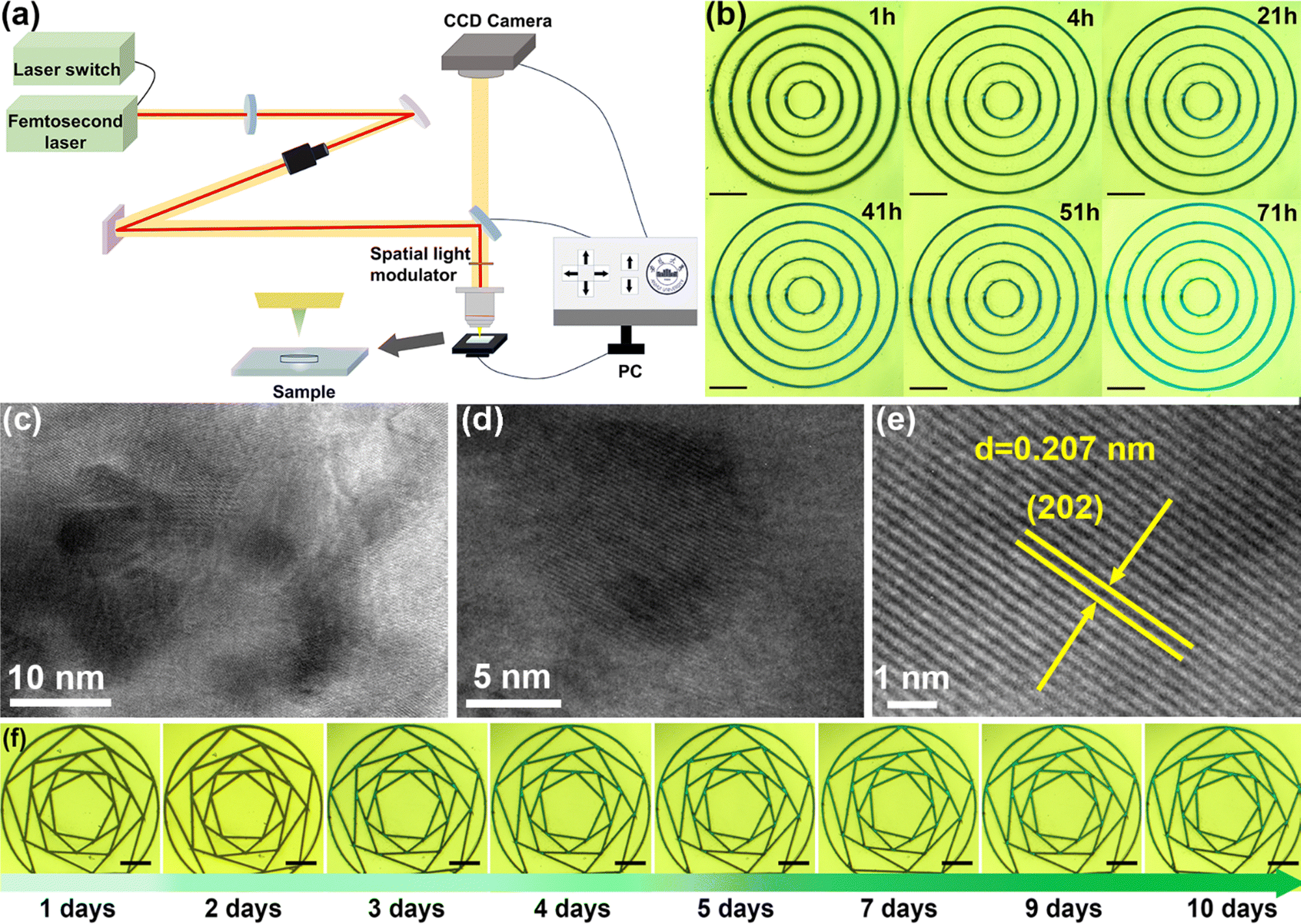 | ||
| Fig. 2 (a) Optical path diagram of fs laser process. (b) Record images of perovskite concentric circle pattern on the surface of phosphate glass under 365 nm UV light after fs LDIP technique (the scale bar is 200 μm). It is observed that perovskite does not precipitate immediately after fs laser processing but rather precipitates slowly, indicating that a slow nucleate and growth process of perovskite. (c)–(e) TEM images of perovskites NCs in the glass matrix with different resolution. (f) Record images of 23.7% perovskite precursor in phosphate glass under 365 nm UV light after fs LDIP technique (the scale bar is 200 μm). | ||
After carving on the glass surface to produce scratches, it is interesting to find that the growth of perovskite will slowly appear in these scratches (Fig. 2), which were precipitate perovskite. The perovskite emits bright green light under 365 nm UV light after a period of time, as shown in Fig. 2b and Movie (ESI†). A detailed photoluminescence spectroscopy (PL) intensity of the sample versus time was recorded immediately after a multiline pattern was drawn using fs LDW technology. It illustrates an increase in PL intensity over time, also confirming the slow precipitation of perovskite inside the glass matrix (Fig. S3, ESI†). The transmission electron microscope (TEM) images at different resolutions comprehensively reveal the growth and distribution of perovskite NCs inside the glass matrix (Fig. 2c–e and Fig. S4, ESI†). The lattice spacing in Fig. 2e was analyzed as 0.207 nm, corresponding to the (202) plane of the monoclinic CsPbBr3 crystal structure, respectively.
Thereby, the main mechanism of laser destruction-induced perovskite growth from phosphate glass is summarized (Fig. 1). After fs laser processing, the dense network structure of the pre-synthesized perovskite precursor composite glass matrix dissociates, with the breakage of P–O–P bonds providing the energy needed for crystal nucleation and growth. Meanwhile, stress is released on the damaged glass surface, and the Cs, Pb, and Br atoms, initially randomly dispersed within the glass, come into closer contact due to the reverse movement shear band effect of the shear stress. When the local stress is beyond a limit, perovskite crystals nucleate and grow. Additionally, the high mobility of Cs+ ions strongly promotes crystal formation.32,33
2.2. Processing patterns on a glass matrix with different perovskite precursor
To further explore the nucleation and growth phenomena, we reduced the perovskite precursor concentration (7Cs2CO3–3PbBr2–5NaBr) in phosphate glasses from 30.7% to 23.7%, by comparing, it was found that both of them were not emitting luminous under the UV light after the fs laser processing was completed at the beginning. However, after 1 hour, when the perovskite precursor was 30.7%, faint luminescence began to appear. This luminescence intensified and spread over time, and the sample achieved full luminescence after 80 hours. This suggests continuous growth of perovskite within the phosphoric glass following its initial disruption until complete precipitation is achieved (as shown in Fig. 2b). For phosphate glass with a 23.7% perovskite precursor, the precipitation of PQDs on the glass surface was completed after 10 days (Fig. 2f). For phosphate glass with a 38.4% perovskite precursor, the precipitation of PQDs on the glass surface was completed after 5 minutes (Fig. S5, ESI†). Therefore, phosphate glasses with higher perovskite precursor concentrations exhibited faster perovskite precipitation rates. The perovskite was almost completely precipitated when the phosphate glass with a 23.7% perovskite precursor, was heated for 4 hours on a 120 °C heating stage. While, the phosphate glass with a 30.7% perovskite precursor, has been completely precipitated after heating at the same temperature for 1 hour (Fig. S6, ESI†).2.3. Structure and optical properties characterization
To verify the properties of laser destruction of phosphate glass-induced growth of perovskite crystals, XRD characterization was performed. The XRD diffraction pattern shown in Fig. 3a reveals peaks corresponding to the (202), (220), and (301) planes of the monoclinic phase CsPbBr3 at 43.69°, 44.14°, and 49.38°, respectively, confirming the identity of the diffraction peaks as characteristic of the monoclinic phase CsPbBr3 (PDF#18-0364). To gain deeper insights into the optical properties of the perovskite nanocrystal-composited phosphate glass, we conducted measurements of room-temperature PL spectra, absorption spectra, and fluorescence lifetimes. As shown in Fig. 3b, the absorption and PL peaks of the sample are located at 511 nm and 519 nm, respectively, indicating a slight Stokes shift. Fig. 3c illustrates the fluorescence lifetime of the sample. The fluorescence lifetime was fitted by a double exponential formula: y = A1 × exp(−x/τ1) + A2 × exp(−x/τ2) + y0, where A1 and A2 are the amplitudes of the two exponential decay components, τ1 and τ2 are their respective decay time constants (A1 = 0.29, A2 = 0.71, τ1 = 62.96 ns, τ2 = 4.06 ns), the average lifetime is calculated as 54.93 ns by the following formula:34 | (1) |
 | ||
| Fig. 3 (a)–(c) The XRD, Absorption, PL and lifetime of the glass surface after perovskites precipitation, respectively. (d) Raman spectra of phosphate glasses with 30.7% and 23.7% perovskites precursor (e) Fourier transform infrared spectroscopy of primitive perovskite composite phosphate glass, the state after femtosecond laser destruction, and the state after perovskite growth. | ||
The phosphate glass consists of a polymer-like structure of phosphate tetrahedral units, commonly represented by “Qn”, where n indicates the number of bridging oxygens in the phosphate tetrahedron (n = 0, 1, 2, 3). When the oxygen–to–phosphorus ratio (O/P) is 3.0, it forms a chain or ring-structured Q2 metaphosphate glass unit.35,36 According to the Raman spectra, the vibration peaks at 490 cm−1 and 782 cm−1 correspond to the v2 band of PO4 in phosphate crystals and the symmetric stretching vibration of P–O–P in the Q2 structure, respectively, which are key components of the phosphate glass structure (Fig. 3d).37 Fourier-transform infrared spectroscopy (FTIR) indicates that, for the pristine perovskite composite glass and after fs laser destructs, the peak at 2964 cm−1 corresponds to the asymmetric stretching vibration of C–H bond,38 and the peak at 2852 cm−1 corresponds to the symmetrical and asymmetric vibrational modes of CH2 groups.39 The key peaks correspond to 570 cm−1 (the bending vibration of PO43− groups), 837 cm−1 (P–O–P stretching vibration), and 1375 cm−1 (PO2− non-bridging oxygen stretching vibration).40 As Pb2+ ions are incorporated into the crystalline phase, they alter the distribution of non-bridging oxygens, thereby weakening their stabilizing effect on the glass network.41 This process promotes the depolymerization of the phosphate glass network, disrupting the original P–O–P bonds and weakening the vibrational intensities at 837 cm−1 and 1375 cm−1. The crystallization process also alters the local structure, leading to the suppression of the vibrational mode around 570 cm−1, which is likely associated with the bending vibrations of PO43− groups. Following glass depolymerization, changes in the chemical environment of the BO3 units lead to instability or reorganization of some B–O bonds, resulting in the weakening of the BO3-related vibration mode at 1446 cm−1 (Fig. 3e).42 Through Raman and FTIR characterization analysis, it can be concluded that following laser processing, perovskite crystals begin to form, accompanied by the breaking of the P–O–P bonds. To investigate the role of P–O–P bonds in perovskite growth, we increase the phosphate content in pristine glass component. We used the same fs laser power to destroy these two different types of perovskite glass. As shown in Fig. S7 (ESI†), when the content of P–O–P bonds in the glass composition is higher, the perovskite glass fully emits light and precipitates perovskite just 1.5 hours after fs laser destruction. This phenomenon suggests that the breaking of the P–O–P bond provides additional energy for perovskite nucleation during the fs laser destruction of the glass. The free energy changes as perovskite forms in a glass matrix with the aid of a fs laser. Starting from a high-energy state, under the influence of a fs laser, the P–O–P bonds of perovskite precursor composite phosphate glass are broken in a very short time, accompanied by the beginning of glass structure depolymerization. The resulting loose structure facilitates ion migration, thereby promoting nucleation. The glass transitions from a tightly connected network structure to a looser one, which not only reduces the energy barrier for nucleation but also increases the rate of ion migration. Additionally, mechanical stress accelerates ion diffusion by lowering the activation energy, further promoting the formation and growth of crystal nuclei. Simultaneously, local stress-induced defects, such as vacancies and dislocations, act as active sites for nucleation, further lowering the energy barrier. While nucleation occurs following laser destruction, crystal growth typically takes hours to days, mainly limited by the rate of ion migration. As Cs+, Pb2+, and Br− ions diffuse and gather, grow into stable monoclinic CsPbBr3 crystals (Fig. S8, ESI†). We measured the surface roughness of the pristine perovskite precursor composite phosphate glass by using an optical profilometer and also examined the patterning of 200 μm line patterns and 1 mm concentric circles of perovskite nanocrystal-composited phosphate glass by fs laser. Sa and Sq were used as the main evaluation parameters. The surface roughness Sa was 16.4 nm, 42.5 nm, 624.8 nm, and Sq was 20.4 nm, 53.4 nm, and 835.9 nm, respectively (see Fig. S9–S11 and Table S1, ESI†).
2.4. Laser-processed fancy patterns
Utilizing the fs LDIP strategy, we also created intricate patterns, including a flower, a shark, and the Anhui University emblem patterns on the glass surface. The patterns, under ambient light (see Fig. 4a), demonstrate neat, clean edges and no splashes with high precision. Fig. 4b shows that the patterns fabricated by fs LDIP emit a distinct green light under 365 nm UV light after a certain period, indicating that perovskite crystals have successfully precipitated in the laser-ablated area. Leveraging the high precision of cold fs LDIP processing, we also fabricated concentric circles, tangram plates, concentric matrices, and QR codes on the glass surface. Scanning electron microscopy (SEM) revealed clear contours (Fig. 4c), further confirming the successful application of fs LDIP technology to high-resolution pattern processing. In addition, we used fs lasers of varying power, repetition rate, and speed to process multiple arrays of 200 μm lines on the glass, in order to explore the minimum fabrication accuracy of this strategy (shown in Fig. S12 and Table S2, ESI†). The results show that our minimum accuracy is 0.83 μm. Compared to other perovskite patterning strategies, our strategy demonstrates excellent accuracy in perovskite patterning. (see Table S3, ESI†).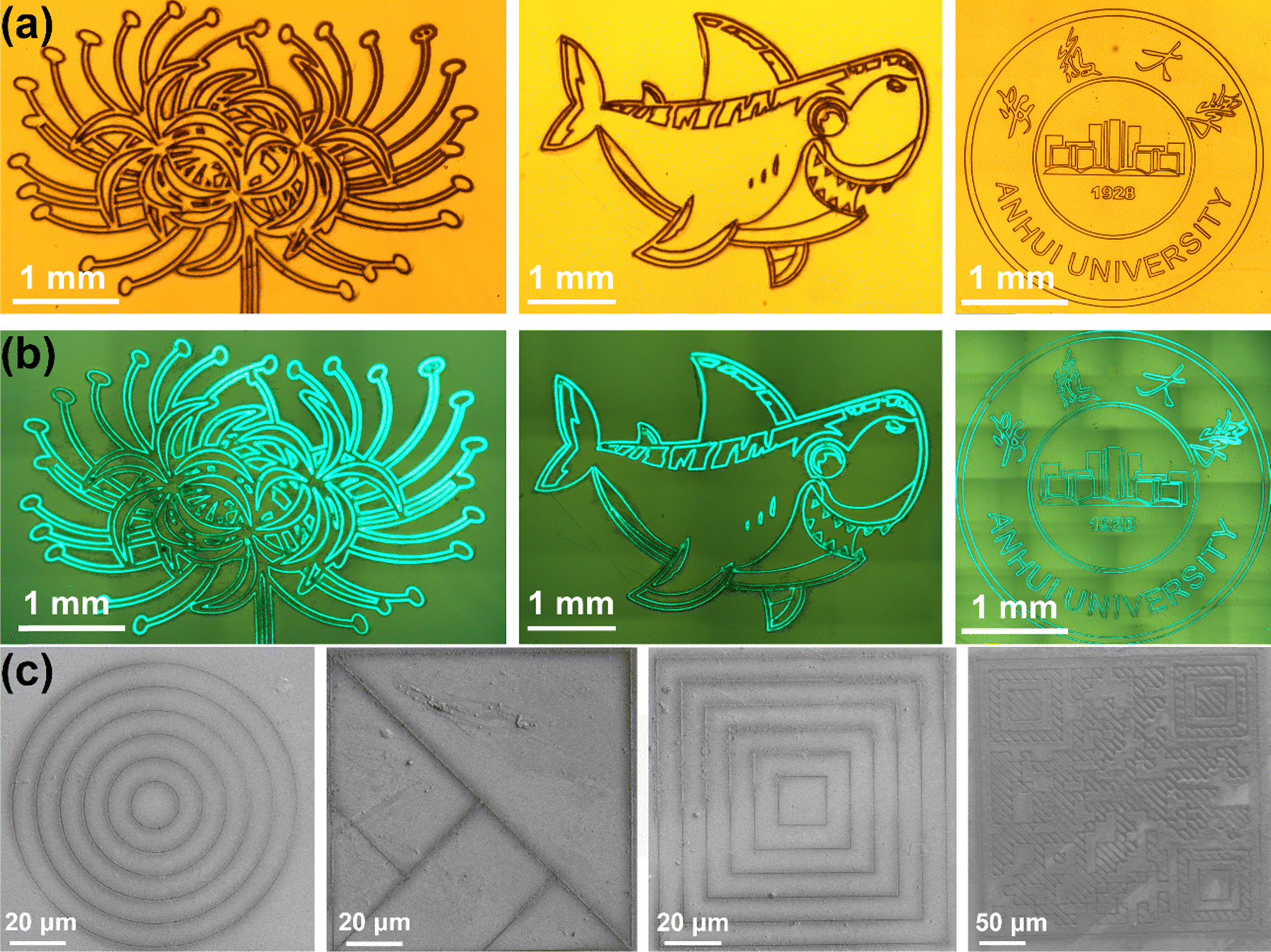 | ||
| Fig. 4 (a) The flower, shark, and Anhui University emblem processed by fs LDW technology under ambient light respectively. (b) The corresponding photos are under 365 nm UV light. (c) The SEM image of concentric circles, tangram, concentric matrix and QR code of 300 μm. | ||
Long-term stability assessments showed that, despite prolonged storage, the patterns maintained bright luminescence due to the protective properties of the glass substrate. (Fig. S13, ESI†). The emission spectra, measured using a spectrometer after several hours of UV exposure, demonstrated stable fluorescence intensity over time (Fig. S14, ESI†). The excellent stability (including storage and optical stability) and high resolution are guaranteed for the practical application of subsequent optoelectronic devices, such as displays, image sensors, and anti-counterfeiting.
2.5. Anti-counterfeiting applications
For anti-counterfeiting applications, we propose the rapid processing of multiple security patterns by our fs LDIP strategy. To enhance the anti-counterfeiting efficiency, a convolutional neural network (CNN) was employed to discern the pattern data, thereby gauging the reliability of the system accurately identifying the anti-counterfeiting pattern. (Fig. 5a). The CNN architecture includes convolutional layers, pooling layers, and fully connected layers.43 An artificial intelligence (AI) system on the computer automatically generates 50 randomly coded images, these images were then processed on the perovskite nanocrystal-composited phosphate glass surface by laser (Fig. S15, ESI†), each featuring a unique identifier derived from the first 12 bits of a SHA256 hash value, generated by combining a key with the hash algorithm. The array images, accompanied by rectangular labels, were generated using a specialized micro-hole array generation program. In each image, pixels representing odd characters in the identifier were rendered black, while even characters corresponded to white pixels, thus forming distinctive rectangular anti-counterfeiting labels.44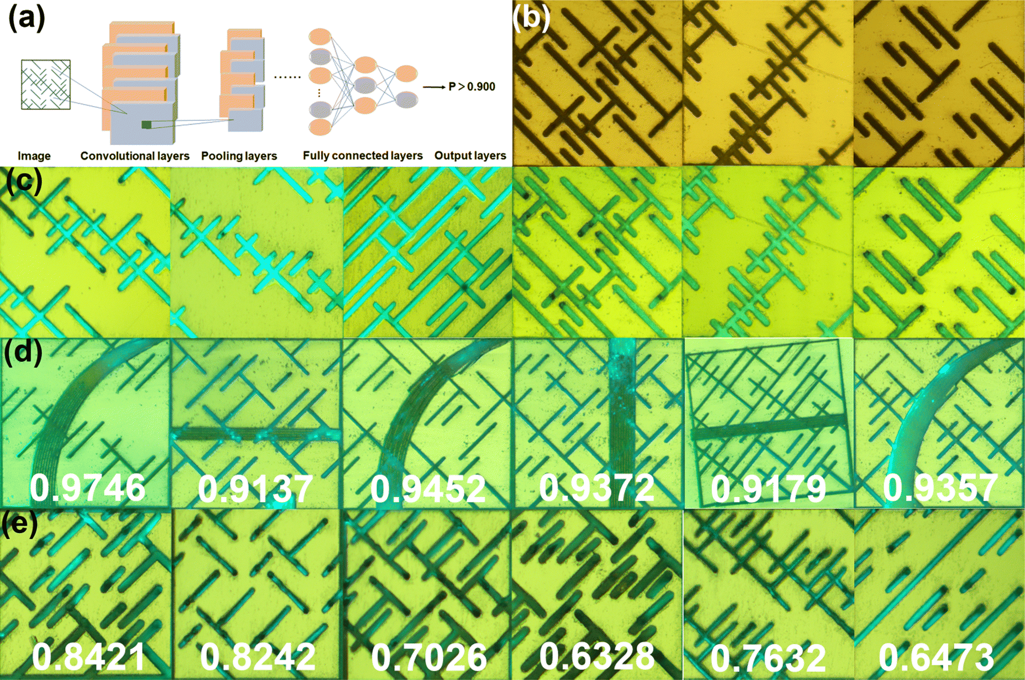 | ||
| Fig. 5 (a) Schematic diagram of a convolutional neural network. (b) Three represent security patterns under ambient light. (c) Six represent 50 anti-counterfeiting images under 365 nm UV light. (d) Simulate pollution and damage caused by real use. (e) False anti-counterfeiting patterns that are similar but not part of the anti-counterfeiting program. | ||
The images of some of the processed anti-counterfeiting patterns under ambient light are shown in Fig. 5b. However, the images are insufficient for anti-counterfeiting applications due to a lack of distinct lines and a low probability of successful recognition. On the contrary, when photographed the sample was under 365 nm UV light, and the pattern lines became more obvious in their luminescence (Fig. 5c). Using convolutional neural networks to identify all patterns formed by laser ablation on perovskite nanocrystal-composited phosphate glass surfaces photographed under 365 nm UV light.
After that, six of the fifty pre-processed patterns were randomly selected, rotated, cut, and damaged to simulate the degradation and deterioration of daily use (Fig. 5d). These anti-counterfeiting products were then re-identified with recognition reliability of 0.9746, 0.9137, 0.9452, 0.9372, 0.9179, and 0.9357, respectively. Following this, we tested the AI's recognition capabilities on six images that were not included in its learning dataset, resulting in recognition reliabilities of 0.8421, 0.8242, 0.7026, 0.6328, 0.7632 and 0.6473 (Fig. 5e), the photos are recognized these as non-anti-counterfeiting patterns. By setting a threshold of 0.9 and considering the confidence level, we can accurately identify the authenticity of the labels. Therefore, the anti-counterfeiting patterns processed by fs lasers based on deep learning methods have the potential to be exceptionally durable and possess strong anti-counterfeiting capabilities.
3. Conclusions
In conclusion, we propose a novel fs LDIP mechanism to fabricate perovskite patterns within a glass matrix. Using fs cold processing, we create precise patterning damage on the glass surface, allowing perovskite NCs to precipitate over time. This laser destruction induced perovskite growth mechanism, bypassing traditional photon absorption and heat accumulation, ensures high precision and adaptability in patterning formation. Furthermore, by integrating artificial intelligence, we generate anti-counterfeiting patterns that are difficult to replicate. Convolutional neural network deep learning accurately identifies these patterns with a success rate exceeding 90%, even under simulated real-world scenarios. This pioneering technique promises to advance the miniaturization of devices and inspire further research in the field.4. Experiment procedure
4.1. Synthesis of the glasses
During the preparation of perovskite precursors composite phosphate glass, 10NaPO3–10KPO3–10ZnO–25/3Al2O3–2Al(PO3)3–80H3BO3–7Cs2CO3–3PbBr2–5NaBr containing 24.081 g (23.7%) and 34.401 g (30.7%) of perovskite precursors were accurately weighed. 15NaPO3–16KPO3–10ZnO–25/3Al2O3–12/5Al(PO3)3–40H3BO3–7Cs2CO3–3PbBr2–5NaBr containing 24.081 g (23.7%) of perovskite precursors was accurately weighed. The weighed powder was evenly mixed and ground in a mortar, then poured into a small furnace to melt. After the furnace temperature reached about 1150 °C, the glass melt was poured into a preheated copper mold to cool, resulting in a transparent glass plate (as shown in Fig. S1, ESI†).4.2. Fs processing platform system used in fs LDW process
The high-power, high-energy fs laser system (MONACO 517) is utilized to generate a laser beam with an emission center wavelength of 517 nm, a pulse width of 350 fs, and a repetition rate of 10 kHz to 750 kHz. It is employed in conjunction with the Roban fs laser micro-nano processing system equipped with and displacement platform (Newport, Model XPS-D). The output power of the laser is controlled by the program control software. During the pattern making process, aperture objective lenses (NA = 0.8 × 100 & NA = 0.45 × 20, Semi APO) are used to focus the pulsed laser. Simultaneously, a CCD camera is equipped to observe whether the laser parameters used are suitable for destructing the structure of the perovskite nanocrystal-composited phosphate glass.4.3. Equipment and methods used in the process of material characterization
The fluorescence images of perovskite patterns on the surface of perovskite nanocrystal-composited phosphate glass were characterized by a microscope (BX53MTRF-S, OLYMPUS). Scanning electron microscopy (SEM) images of patterned perovskite were captured using a scanning electron microscopy (SEM) facility (Regulus 8230, Hitachi). Transmission electron microscopy (TEM) images were obtained using equipment (JEM-F200, JEOL). The PL test system consists of a laser (LASERLAND) with a wavelength range of 405 nm, a microscope (YM710R, YUESCOPE), and a spectrometer (QE65Pro, OCEAN INSIGHT). By using an X-ray diffractometer (Empyrean S3, Malvern Panalytical) to study the internal structure of the material written by fs laser, the XRD pattern corresponding to perovskite nanocrystal-composited phosphate glass is obtained. The fluorescence lifetime of perovskite was evaluated using a time-resolved fluorescence spectrometer (FluoroMax Plus, Horiba). The perovskites grown by fs laser processing were characterized and analyzed by these instruments and methods. Micro-Raman spectroscopy measurements were conducted by using a Horiba (LabRAM Odyssey) spectrometer equipped with a liquid nitrogen-cooled charge-coupled device (CCD) and solid-state lasers with wavelengths of 633 nm. Raman spectra were collected by using an 1800 grooves per mm grating in the 400–4000 cm−1 range with a 50× objective lens. A very good signal-to-noise ratio was obtained with 30 s integration time for each spectrum. The absorption is measured using a home-built microscope equipped with a Tungsten lamp as the white light source. The samples were examined using a Bruker (VERTEX80v) FTIR equipped with a liquid nitrogen-cooled infrared detector. The sample was placed under the microscope objective lens, and the signal was collected using the transmission mode of the spectrometer to measure the infrared spectrum in the wave number range of 400–4000 cm−1. These parameters were measured using a Bruker Contour GT 3D Optical Profilometer. The raw data obtained from the measurements were analyzed using Bruker's Vision 64 software, which provided detailed insights into the surface roughness characteristics.4.4. This convolutional neural network model consists of the following components
Five convolutional layers: these five convolutional layers are used to extract features from the anti-counterfeiting label images. The first layer uses 96 11 × 11 convolutional kernels, the second layer uses 256 5 × 5 convolutional kernels, the third and fourth layers use 384 3 × 3 convolutional kernels, and the fifth layer uses 256 3 × 3 convolutional kernels. Five ReLU activation layers: each convolutional layer is followed by a ReLU activation function. Three max-pooling layers: there is a 3 × 3 max-pooling layer after the first, second, and fifth ReLU activation layers. Three fully connected layers: during training, dropout is applied to the fully connected layers to prevent overfitting. The first fully connected layer has 512 nodes, followed by a LeakyReLU activation function and dropout (with a dropout rate of 0.5). The second fully connected layer also has 512 nodes, followed by a LeakyReLU activation function and dropout (with a dropout rate of 0.5). Dropout is used to prevent overfitting during training.Author contributions
S. Li provided the overall concept and revised the manuscript. S. Liu and X. Xu conducted the experiments and wrote the manuscript. J. Zhou, Y. Jiang, and Y. Kuai helped with the experimental test. B. Yu helped revise the manuscript. All authors contributed to the general discussion.Data availability
Data are available upon request from the authors.Conflicts of interest
The authors declare that they have no conflict of interest.Acknowledgements
This work was financially supported by the National Natural Science Foundation of China (Grant No. 62205002 and 62205003), the Anhui Provincial Natural Science Foundation (Grant No. 2208085QA19), the Education Department of Anhui Province (Grant No. 2023AH020004).Notes and references
- G.-D. Ye, S.-H. Li, R. Ding, R. Guo, H. Zhang, Z.-Q. Liu, F. Yang, L. Sun, Y. Li, X. Du, X.-B. Wang, L. Wang, Y.-F. Liu, H.-H. Fang, Y. Liu, B. Xu and J. Feng, SmartMat, 2025, 6, e1329 CAS.
- S.-H. Chin, J. Opt. Photonics Res., 2024, 1–9 CAS.
- X. Zhang, Z. Li, E. Hong, T. Yan and X. Fang, Adv. Mater., 2025, 37, 2412014 CAS.
- Z. Wang, S. Li, G. Ren, S. Yao, D. Zhu, J. Xie, J. Zhou, X. Xu, W. Huang, Y. Kuai, C. M. Wan, J. Ye, X. Xu and Z. Hu, ACS Photonics, 2024, 11, 3003–3011 CrossRef CAS.
- L. Zhang, L. Mei, K. Wang, Y. Lv, S. Zhang, Y. Lian, X. Liu, Z. Ma, G. Xiao, Q. Liu, S. Zhai, S. Zhang, G. Liu, L. Yuan, B. Guo, Z. Chen, K. Wei, A. Liu, S. Yue, G. Niu, X. Pan, J. Sun, Y. Hua, W.-Q. Wu, D. Di, B. Zhao, J. Tian, Z. Wang, Y. Yang, L. Chu, M. Yuan, H. Zeng, H.-L. Yip, K. Yan, W. Xu, L. Zhu, W. Zhang, G. Xing, F. Gao and L. Ding, Nano-Micro Lett., 2023, 15, 177 CrossRef PubMed.
- D. Wang and G. Li, Laser Photonics Rev., 2022, 16, 2100713 CrossRef.
- M. Shi, R. Li and C. Li, EcoMat, 2021, 3, e12074 CrossRef CAS.
- X. Guan, Z. Lei, X. Yu, C.-H. Lin, J.-K. Huang, C.-Y. Huang, L. Hu, F. Li, A. Vinu, J. Yi and T. Wu, Small, 2022, 18, 2203311 CrossRef CAS PubMed.
- L. Chouhan, S. Ghimire, C. Subrahmanyam, T. Miyasaka and V. Biju, Chem. Soc. Rev., 2020, 49, 2869–2885 RSC.
- S. Yuhang, W. Xiaoming, J. Baohua and G. Zhixing, Light: Adv. Manuf., 2024, 4, 95–116 Search PubMed.
- X. Huang, Q. Guo, D. Yang, X. Xiao, X. Liu, Z. Xia, F. Fan, J. Qiu and G. Dong, Nat. Photonics, 2020, 14, 82–88 CrossRef CAS.
- K. Sun, D. Tan, X. Fang, X. Xia, D. Lin, J. Song, Y. Lin, Z. Liu, M. Gu, Y. Yue and J. Qiu, Science, 2022, 375, 307–310 CrossRef CAS PubMed.
- Z. Wan, Z. Liu, Q. Zhang, Q. Zhang and M. Gu, Adv. Mater. Technol., 2024, 9, 2302033 CrossRef CAS.
- L. Hu, P. Zuo, F. Li, H. Tian, H. Huang, T. Liu and D. Zhu, Opt. Laser Technol., 2024, 176, 110877 CrossRef CAS.
- X. Xu, S. Liu, Y. Kuai, Y. Jiang, Z. Hu, B. Yu and S. Li, Adv. Sci., 2024, 11, 2309862 CrossRef CAS PubMed.
- S.-Y. Liang, Y.-F. Liu, Z.-K. Ji, S.-Y. Wang, H. Xia and H.-B. Sun, Nano Lett., 2023, 23, 3769–3774 CrossRef CAS PubMed.
- S.-Y. Liang, Y.-F. Liu, H.-J. Zhang, Z.-K. Ji and H. Xia, ACS Appl. Mater. Interfaces, 2022, 14, 46958–46963 CrossRef CAS PubMed.
- W. Kong, C. Zhao, J. Xing, Y. Zou, T. Huang, F. Li, J. Yang, W. Yu and C. Guo, Sol. RRL, 2020, 4, 2000189 CrossRef CAS.
- A. Cherepakhin, A. Zhizhchenko, D. Khmelevskaia, L. Logunov, A. Kuchmizhak and S. Makarov, Adv. Opt. Mater., 2024, 12, 2302782 CrossRef CAS.
- B. Xu, T. Man, X. Yu, X. Cai, Z. Zhou, D. Tan and J. Qiu, Adv. Photonics Res., 2024, 2400047 CrossRef CAS.
- Y. Hu, W. Zhang, Y. Ye, Z. Zhao and C. Liu, ACS Appl. Nano Mater., 2020, 3, 850–857 CrossRef CAS.
- X.-G. Chen, L. Lin, G.-Y. Huang, X.-M. Chen, X.-Z. Li, Y.-K. Zhou, Y. Zou, T. Fu, P. Li, Z. Li and H.-B. Sun, Nat. Commun., 2024, 15, 3677 CrossRef CAS PubMed.
- X. Huang, X. Xiao and G. Dong, Adv. Mater. Technol., 2020, 5, 2000513 CrossRef.
- W. Zhan, L. Meng, C. Shao, X.-G. Wu, K. Shi and H. Zhong, ACS Photonics, 2021, 8, 765–770 CrossRef CAS.
- L. Nie, T. Wang, X. Yu, W. Gao, Q. Peng, Z. Xia, J. Qiu, S. F. Yu and X. Xu, ACS Energy Lett., 2023, 8, 2025–2032 CrossRef CAS.
- C. Ge, Y. Li, H. Song, Q. Xie, L. Zhang, X. Ma, J. Liu, X. Guo, Y. Yan, D. Liu, W. Zhang, S. Liu and Y. Liu, Nat. Commun., 2024, 15, 914 CrossRef CAS PubMed.
- K. Sugioka and Y. Cheng, Light Sci. Appl., 2014, 3, e149 CrossRef CAS.
- K. Sugioka and Y. Cheng, Appl. Phys. Rev., 2014, 1, 041303 Search PubMed.
- S. Wang, J. Yang, G. Deng and S. Zhou, Materials, 2024, 17, 557 CrossRef CAS PubMed.
- X. Wang, H. Yu, P. Li, Y. Zhang, Y. Wen, Y. Qiu, Z. Liu, Y. Li and L. Liu, Opt. Laser Technol., 2021, 135, 106687 CrossRef CAS.
- B. Dong, J. Zhang, D. Wang, Y. Zhang, L. Zhang, R. Li, C. Xin, S. Liu, Z. Zhang, H. Wu, S. Jiang, S. Zhu, B. Liu and D. Wu, Opto-Electron. Eng., 2023, 50, 220073 Search PubMed.
- X. Xiang, H. Lin, R. Li, Y. Cheng, Q. Huang, J. Xu, C. Wang, X. Chen and Y. Wang, Nano Res., 2019, 12, 1049–1054 CrossRef CAS.
- R. Zheng, J. Ueda, K. Shinozaki and S. Tanabe, Chem. Mater., 2022, 34, 1599–1610 CrossRef CAS.
- S. Li, D. Lei, W. Ren, X. Guo, S. Wu, Y. Zhu, A. L. Rogach, M. Chhowalla and A. K. Y. Jen, Nat. Commun., 2020, 11, 1192 CAS.
- B. Alhasni, J. Non-Cryst. Solids, 2022, 578, 121338 CrossRef CAS.
- Z. Černošek, M. Chládková and J. Holubová, J. Solid State Chem., 2022, 314, 123366 CrossRef.
- Y. Tao, S. Fangfang, W. Junxia and L. X. Feng, Glasses, 2018, 45, 6–10 Search PubMed.
- K. Kurniawan, M.-S. Kim, K. W. Chung, R. Kim and J.-C. Lee, Sep. Purif. Technol., 2021, 255, 117712 Search PubMed.
- A. Z. Hameed, D. Parbat and S. J. Lee, Chem. Eng. J., 2023, 477, 147062 CAS.
- P. K. Jha, O. P. Pandey and K. Singh, J. Mol. Struct., 2015, 1083, 278–285 CAS.
- E. Banoqitah, F. Djouider, M. R. Alnowaimi, A. M. Alhawsawi, E. B. Moustafa and A. H. Hammad, J. Mater. Sci. Mater. Electron., 2024, 35, 974 CAS.
- T. Edwards, T. Endo, J. H. Walton and S. Sen, Science, 2014, 345, 1027–1029 CAS.
- S. Cong and Y. Zhou, Artif. Intell. Rev., 2023, 56, 1905–1969 Search PubMed.
- S.-Y. Liang, Y.-F. Liu, S.-Y. Wang, Z.-K. Ji, H. Xia, B.-F. Bai and H.-B. Sun, Adv. Funct. Mater., 2022, 32, 0224957 CAS.
Footnotes |
| † Electronic supplementary information (ESI) available. See DOI: https://doi.org/10.1039/d4nh00612g |
| ‡ These two authors are joint first authors. |
| This journal is © The Royal Society of Chemistry 2025 |