
Development and challenges of polarization-sensitive photodetectors based on 2D materials
Liang
Yu
a,
Huafeng
Dong
a,
Wei
Zhang
a,
Zhaoqiang
Zheng
 *b,
Ying
Liang
*c and
Jiandong
Yao
*d
*b,
Ying
Liang
*c and
Jiandong
Yao
*d
aSchool of Physics and Optoelectronic Engineering, Guangdong University of Technology, Guangzhou 510006, China
bGuangdong Provincial Key Laboratory of Information Photonics Technology, Guangdong Provincial Key Laboratory of Functional Soft Condensed Matter, School of Materials and Energy, Guangdong University of Technology, Guangzhou 510006, Guangdong, P. R. China. E-mail: zhengzhq5@mail2.sysu.edu.cn
cSchool of Arts and Sciences, Guangzhou Maritime University, Guangzhou 510799, Guangdong, P.R. China. E-mail: liangysysu@163.com
dState Key Laboratory of Optoelectronic Materials and Technologies, Nanotechnology Research Center, School of Materials Science & Engineering, Sun Yat-sen University, Guangzhou 510275, Guangdong, P. R. China. E-mail: yaojd3@mail.sysu.edu.cn
First published on 5th February 2025
Abstract
Polarization-sensitive photodetectors based on two-dimensional (2D) materials have garnered significant research attention owing to their distinctive architectures and exceptional photophysical properties. Specifically, anisotropic 2D materials, including semiconductors such as black phosphorus (BP), tellurium (Te), transition metal dichalcogenides (TMDs), and tantalum nickel pentaselenide (Ta2NiSe5), as well as semimetals like 1T′-MoTe2 and PdSe2, and their diverse van der Waals (vdW) heterojunctions, exhibit broad detection spectral ranges and possess inherent functional advantages. To date, numerous polarization-sensitive photodetectors based on 2D materials have been documented. This review initially provides a concise overview of the detection mechanisms and performance metrics of 2D polarization-sensitive photodetectors, which are pivotal for assessing their photodetection capabilities. It then examines the latest advancements in polarization-sensitive photodetectors based on individual 2D materials, 2D vdW heterojunctions, nanoantenna/electrode engineering, and structural strain integrated with 2D structures, encompassing a range of devices from the ultraviolet to infrared bands. However, several challenges persist in developing more comprehensive and functional 2D polarization-sensitive photodetectors. Further research in this area is essential. Ultimately, this review offers insights into the current limitations and challenges in the field and presents general recommendations to propel advancements and guide the progress of 2D polarization-sensitive photodetectors.
1. Introduction
Photodetectors are fundamental components in light sensing systems, playing a vital role across diverse domains including remote sensing, environmental monitoring, and medical diagnostics.1–4 The advancement of photodetectors is primarily steered by emerging technologies such as photonic integrated circuits, the Internet of Things (IoT), and automation.5–7 These technologies continually propel improvements in photodetector performance and capabilities, enabling them to achieve advanced functionalities such as wide wavelength detection and polarization-sensitive photoresponse.Light is an electromagnetic wave encapsulating essential elements like intensity, wavelength, phase, and polarization. While the human eye can perceive light intensity within a constrained wavelength range (approximately 390–760 nm),8,9 a deeper understanding of light is essential for comprehensive exploration of our surroundings. Human ingenuity allows us to effectively alter existing conditions through the judicious application of tools. Among these tools, photodetectors are indispensable instruments for unraveling the mysteries of light. They possess the remarkable ability to convert the intricate properties of light into electric currents, rendering them perceivable to human senses. Notably, the polarization of light, characterized by its vector properties, poses a challenge for intuitive human observation. However, the detection of polarized light holds critical applications across diverse fields. In the realm of biology and medicine, polarized light detection has become a valuable tool for studying biological structures and physiological processes. Polarization-sensitive imaging techniques, such as polarization microscopy, can provide deep insights into the dynamics of cells, tissues, and biomolecules, thereby facilitating the diagnosis and monitoring of various medical conditions.10,11 Furthermore, polarization-sensitive photodetectors can distinguish between different polarization states of light, enabling the acquisition of vast amounts of information about the properties and interactions of light with matter. This knowledge has been instrumental in driving advancements across a wide range of disciplines, from quantum computing to materials science.12,13 Therefore, the development of detectors tailored for polarized light detection is of paramount importance.
The concept of designing polarization-sensitive photodetectors dates back half a century,14,15 yet early iterations often sacrificed compactness to fulfill their objectives,16–18 hindering widespread adoption. Recent years have witnessed the emergence of micro-nano photodetectors,19–21 marking a significant leap in technology. Since the inception of the first graphene (Gr) nanosheet in 2004, two-dimensional (2D) materials have stepped into the forefront of photodetector technology. Leveraging their distinctive properties, these materials have emerged as the premier option for micro-nano photodetectors.
After years of advancement, micro-nano photodetectors boasting enhanced photoresponsivity and rapid response attributes have found widespread utility in realms such as communications, biomedicine, and remote sensing.22–24 Yet, the current landscape reveals a limitation: although traditional photodetectors crafted from materials like silicon (Si), germanium (Ge), and III–V semiconductors exhibit superior sensitivity, it is difficult to distinguish polarized light. 2D materials are an effective solution to solving this issue. They exhibit strong light–matter interactions, adjustable band gaps based on thickness, and high carrier mobility that greatly enhance the performance of photodetectors. Additionally, their high extinction ratio allows them to overcome problems caused by signal crosstalk in traditional detectors.25,26 Moreover, they also possess significant linear/nonlinear photoresponse and an ultra-fast energy transfer rate.27–29 Most crucially, due to their rich band structures and naturally passivated surfaces, 2D materials with different capabilities can be artificially stacked to form homogeneous/heterogeneous junctions to maximize functionality.30–34 Additionally, 2D materials can easily integrate with 1D/3D structures to enhance their inherent capabilities.25,35 These abilities grant 2D materials with significant flexibility in the field of photodetectors.
In recent years, numerous polarization-sensitive photodetectors based on 2D materials have emerged, capable of detecting polarized light. These include devices utilizing semiconductor materials such as ReSe2,36 ReS2,37 GeSe,38 GeS2,39 as well as semi-metallic materials like1T′-MoTe234 and PdSe2.40 Previous studies have demonstrated the flexible application of these 2D materials in various photodetector designs, leveraging their unique properties. Additionally, there have been reports of combining nanoantennas with 2D materials for polarized light detection.25,41 Furthermore, some studies have explored alternative methods, such as strain engineering, to achieve polarized light detection (Fig. 1).42,43
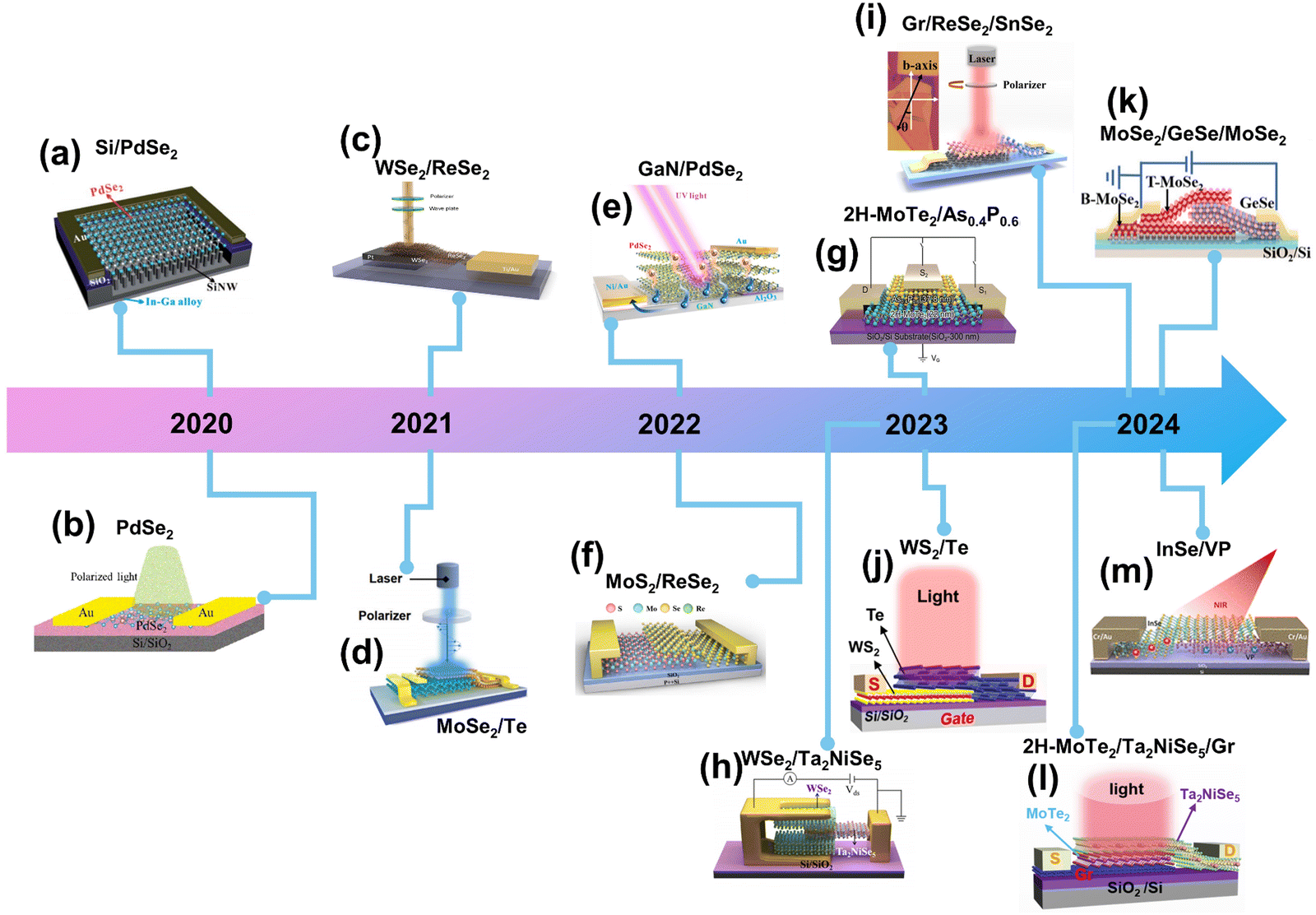 | ||
| Fig. 1 Development of 2D polarization-sensitive photodetectors in the past five years. (a) Reproduced with permission.44 Copyright 2020, The Royal Society of Chemistry. (b) Reproduced with permission.45 Copyright 2020, Tsinghua University Press. (c) Reproduced with permission.46 Copyright 2021, American Chemical Society. (d) Reproduced with permission.47 Copyright 2021, The Royal Society of Chemistry. (e) Reproduced with permission.48 Copyright 2022, American Chemical Society. (f) Reproduced with permission.49 Copyright 2022, The Chinese Ceramic Society. (g) Reproduced with permission.50 Copyright 2023, Wiley-VCH GmbH. (h) Reproduced with permission.51 Copyright 2023, American Chemical Society. (i) Reproduced with permission.36 Copyright 2024, Wiley-VCH GmbH. (j) Reproduced with permission.30 Copyright 2023, Wiley-VCH GmbH. (k) Reproduced with permission.38 Copyright 2024, Wiley-VCH GmbH. (l) Reproduced with permission.52 Copyright 2024, Wiley-VCH GmbH. (m) Reproduced with permission.53 Copyright 2024, American Chemical Society. | ||
Although there have been some discussions on 2D polarization-sensitive photodetection, a detailed and up-to-date systematic description remains lacking. Therefore, it is imperative to provide a comprehensive classification and organization of existing 2D polarization-sensitive photodetectors. This review examines the key applications of 2D materials in polarized light detection over the past five years, with a focus on the working principles and latest research advancements of 2D material-based polarization-sensitive photodetectors. This review categorizes these devices into three main types: single anisotropic material devices, anisotropic material heterostructure devices, and nanoantenna/electrode engineering and structural strain devices. This classification effectively encompasses the majority of 2D material-based polarization-sensitive photodetectors. Subsequently, the latest research findings are introduced and compared. Finally, the ongoing challenges and opportunities in this field are summarized, and potential strategies to address them are envisioned, aiming to guide explorations and fully leverage the pivotal role of 2D materials in the future optoelectronic industry.
2. Polarization-sensitive photodetection mechanism
Before we delve into our discussion, it is essential to introduce the working mechanism of 2D polarization-sensitive photodetectors, explaining how they convert polarized light into polarization-dependent currents. Additionally, we need to discuss the parameters used to evaluate the performance of photodetectors and their definitions. This chapter is divided into two main sections: the first section will focus on the general working principles of photodetectors, explaining how they operate to convert light into an electrical signal. The second section will provide details on the working principles of 2D polarization-sensitive photodetectors specifically, including how they are able to detect the polarization state of incident light.2.1 Working mechanism of photodetectors
Converting light signals into electrical signals is crucial for photodetectors. This process primarily involves the conversion of incident photons into charge carriers or current within the device. The primary working mechanisms include the photoconductive effect, photogating effect, photo-thermoelectric effect, photovoltaic effect, and pyro-phototronic effect.26,54,55 In the following sections, we will introduce each of these mechanisms individually.The processes of photoconductive effect and photogating effect require the application of bias voltage to generate current in the device. In the case of the photoconductive effect, the increase in conductivity is primarily attributed to the increase in photo-generated charge carriers in the semiconductor under illumination.56,57 The applied external voltage causes charge carriers to move in opposite directions, resulting in the photocurrent. The photogating effect is considered a special type of photoconductive effect, where electrons or holes generated by incident light are captured by carrier traps within the semiconductor. The captured carriers have a longer lifetime compared to the transit time of other carriers in the channel, thus modulating the semiconductor's conductivity.58,59 Simultaneously, charged traps in the material can act as local gates, introducing a photo-induced gate voltage to effectively control the conductivity of the channel. For 2D devices, introducing the photogating effect is a crucial method for enhancing their electrical performance.
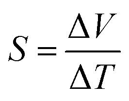
The photo-thermoelectric effect generally exists in photo-thermoelectric devices. In these devices, local heating caused by laser irradiation leads to temperature differences (ΔT) between the two ends of the channel,60 resulting in the generation of photo-thermoelectric voltage difference (ΔV). The ratio of the ΔV to the ΔT is the Seebeck coefficient (S):61
 | (1) |
Under illumination, photo-generated electron–hole pairs are separated by the built-in electric field at the heterojunction interface and collected by the electrodes, a phenomenon known as the photovoltaic effect.62 This effect is commonly utilized in photodiodes, as they can generate current without the need for an external bias voltage, endowing these devices with self-powering capabilities. The appropriate built-in electric field is crucial for this effect, making it widely applicable in Schottky junctions (metal–semiconductor).55,63,64 It is worth mentioning that the open-circuit voltage and the short-circuit current are two essential parameters of photovoltaic devices and key indicators for evaluating the self-powering capabilities of the devices. The pyro-phototronic effect is a working mechanism that has emerged in recent years based on the pyroelectric effect. It refers to the transient temperature changes affecting the photocurrent of a detector at the moment a laser is turned on or off. These temperature fluctuations induce a pyro-electric polarization field in the pyroelectric material, which, combined with the existing built-in electric field, collectively governs the separation of photo-generated electron–hole pairs.65–67 When utilized appropriately, this effect can also serve as an effective method for enhancing the performance of photodetectors.
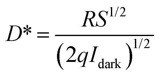
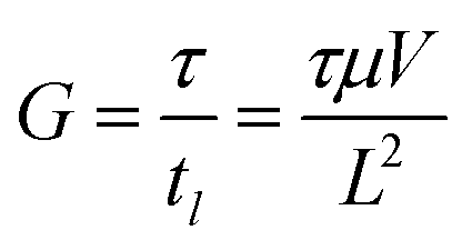
There are many parameters for evaluating the performance of photodetectors, among which the most concerned are responsivity (R), specific detectivity (D*), on/off ratio (Ion/Ioff) and response time (τrise/τfall).68–70 Specifically, R indicates the photoresponse intensity of the device, D* and Ion/Ioff indicate the sensitivity of the device to the environment, τrise/τfall, indicate the response speed of the device. Another two parameters that can directly affect the performance of the device, internal quantum efficiency (IQE) and external quantum efficiency (EQE) are also concern. In addition, noise equivalent power (NEP) represents the minimum optical signal power that the device can detect from the total noise. Photoconductive gain (G) is also valued in photoconductive devices. In order to gain a more detailed understanding of these parameters, Table 1 presents their definitions and formulas in detail.71–74 Among them, there are generally two most commonly used formulas for calculating D*, both of which are listed in the table. However, D* calculated using NEP can often more persuasively represent the sensitivity of the device. Therefore, the D* performance mentioned later in this review are all derived from the NEP formula.
| Parameter | Expression | Description |
|---|---|---|
| Photocurrent (Iph, A) | I ph = Ilight − Idark | I light and Idark respectively represent the photodetector current under laser illumination and in the dark state. |
| Responsivity (R, A W−1) |
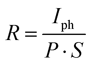
|
R is defined as the ratio of photocurrent to incident optical power density, where P represents the incident optical power density, and S denotes the effective photosensitive area of the device. |
| Noise equivalent power (NEP, W Hz−1/2) |
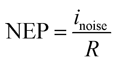
|
NEP refers to the minimum optical signal power that can be detected or distinguished from the total noise. The inoise is the noise current. photodetector. |
| Specific detectivity (D*, Jones) |
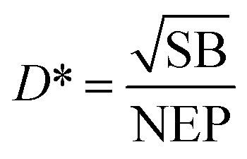
|
B is the bandwidth. |
|
q is the electronic charge. | |
| Photoconductive gain (G) |
|
τ is the photocarrier lifetime, tl is the carrier transit time. The transit time is dependent on the applied bias voltage (V), carrier mobility (μ) and the length of the channel (L). |
| External quantum efficiency (EQE) |
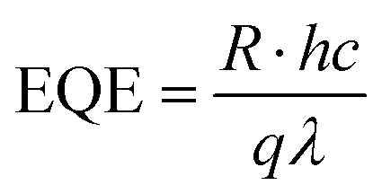
|
EQE is defined as the photon utilization ratio, which is the ratio of the number of incident photons to the number of generated excitons. The h is the Planck constant (6.626 × 10⁻³⁴ J s−1), c is the light velocity, λ is the wavelength of incident. light, |
| Internal quantum efficiency (IQE) |
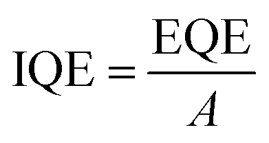
|
Where A is the absorption coefficient of the material. The IQE formula mainly considers the number of photons absorbed. |
| Response time (τrise/τfall, s) | τ rise and τfall | τ rise and τfall are defined as the time measured from 10%/90% to 90%/10% of the net photocurrent. |
| On/off ratio (Ion/Ioff) |
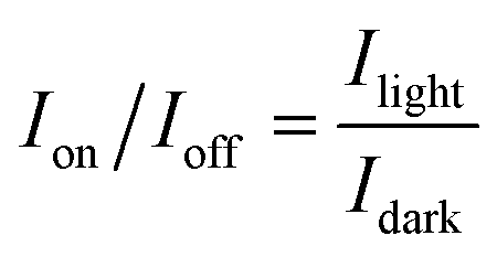
|
I on/Ioff refers to the ratio of photodetector current under laser illumination to dark current. |
2.2 Working mechanism of polarization-sensitive photodetectors
To systematically understanding the photoresponse mechanism of the polarization-sensitive photodetectors, the constitutive relation containing nonlinear terms is firstly discussed. The electric field E(t) can be written as:26,75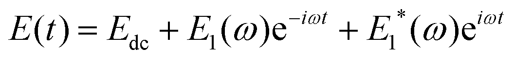 | (2) |
| Jidc = σ(1);ijdc(0)Ejdc + 2σ(2);ikm(ω, −ω)Ek1(Em1)* + 6σ(3);ikm(0, ω, −ω)Ejdc(Em1)* + … | (3) |
| Jidc = σ(1)E(1) + σ(2)EE +… | (4) |
Under light illumination, the current change is completely determined by the nonlinear conductivity tensors σ(2) and σ(3). When these components exhibit anisotropy depending on the different directions of the dc field and optical field. The change in photocurrent density under different polarized light excitations can be expressed as:
| ΔJidc = ΔΔσ(1)·Ejdc + σ(2)·EE +… = ΔσΔE·Ejdc + σ(2)·EE +… | (5) |
The polarization performance of the photodetector can be affected by varying the parameters in eqn (5). In addition, a crucial metric for evaluating the polarization performance of photodetectors is the polarization ratio (PR).76–78 Although various definitions and expressions of this parameter exist in different articles, the fundamental definition remains consistent. Essentially, there are two primary expression methods: one using (Imax − Imin)/(Imax + Imin),33 while the other using Imax/Imin.34,77 In this review, we uniformly express the PR as the ratio of the maximum to minimum photocurrent (PR = Imax/Imin). A higher value of PR indicates a stronger ability of the device to discriminate between polarization angle differences.
3. Polarization-sensitive photodetectors based on individual 2D materials
The study of polarization-sensitive photodetectors based on low-dimensional materials dates back to 2001.76 Initially, one-dimensional (1D) nanowires, characterized by their unique structure, garnered significant attention in the research of micro/nano polarization-sensitive photodetectors. Subsequently, 2D materials with asymmetric structures have been reported to enable the detection of polarized light. Notably, over the past five years, 2D materials have garnered considerable interest, prompting researchers to explore their potential for detecting polarized light and assess their practical applications. In this section, we review several representative polarization-sensitive photodetectors based on individual 2D materials from recent years. For ease of comparison and reference, the performance parameters of these devices are summarized in Table 2.| Material | Wavelength (nm) | R (A W−1) | D* (Jones) | τ rise/τfall (ms) | PR | Ref. |
|---|---|---|---|---|---|---|
| GeSe | 532 | 1.6 × 10⁵ | 2.9 × 10¹³ | — | 1.3 | 79 |
| GeSe | 830 | 400 | — | 5.0/2.0 | 2.16 | 80 |
| GeSe | 633 | 7.5 | 3.04 × 10⁸ | — | 1.55 | 81 |
| GeSe | 808 | 30 | — | — | 1.1 | 35 |
| ReSe2 | 635 | 0.379 | 6.8 × 10¹¹ | 18.8/21.6 | 3.1 | 82 |
| ReS2 | 665 | 959 | 1.61 × 10¹² | 130/160 | 1.72 | 83 |
| ReS2 | 650 | 0.28 | 4.22 × 10⁹ | 2.63/2.11 | 2.79 | 84 |
| 1T′-MoTe2 | 850 | 1.2 | 7.68 × 10¹² | 0.016/0.007 | 1.2 | 85 |
| PdSe2 | 532 | 0.0013 | 2.55 × 10⁷ | 0.004/0.014 | 1.3 | 86 |
| PdSe2 | 532 | 0.035 | — | 11/6 | 1.9 | 45 |
| PdSe2 | 7400 | — | 6.7 × 10⁶ | 0.047/0.051 | 2.06 | 87 |
| PdSe2 | 1064 | 1.1 | 1.3 × 10¹¹ | 0.003/0.006 | 1.6 | 88 |
| SiP | 365 | 17 | 2.5 × 10¹¹ | 0.06/0.03 | — | 89 |
| 532 | — | — | — | 2.9 | ||
| Te | 1550 | 327 | 6.08 × 10⁷ | 0.022/0.023 | 2.05 | 90 |
| t-InTe | 365 | 12.05 | 3.85 × 10¹¹ | 100/200 | 91 | |
| 808 | 8.37 | 2.68 × 10¹¹ | — | 1.81 | ||
| VP | 520 | 341 | — | — | 3.9 | 92 |
| In2Te5 | 445 | 0.171 | 5.08 × 10⁹ | — | 1.26 | 93 |
| 638 | 0.139 | 4.13 × 10⁹ | 420/530 | 1.34 | ||
| β-Bi2O3 | 365 | 71.91 | 6.09 × 10¹³ | 0.4/0.2 | 1.91 | 94 |
| Ta2NiSe5 | 638 | 13 | 3.5 × 10¹⁰ | 0.012/0.010 | 1.47 | 95 |
| Ta2NiSe5 | 1064 | 44 | 1.2 × 10¹² | 98/82 | 3.24 | 96 |
| Ta2NiSe5 | 1350 | 198.1 | 3.3 × 10⁹ | 27.4/28.3 | 1.46 | 97 |
| PbSnS2 | 520 | 21.9 | — | 72/8 | 1.25 | 98 |
| In2SnS4 | 532 | 0.0934 | 8.49 × 10⁷ | 0.02/0.02 | 1.7 | 99 |
Germanium selenide (GeSe) is a very classical anisotropic 2D material. It has a similar structure to black phosphorus (BP), holding strong in-plane anisotropy, making it very suitable for application in polarization-sensitive photodetectors. However, unlike BP, GeSe is very stable in air. As early as 2012, Xue et al.100 first reported the liquid phase synthesis of GeSe nanosheets and characterized the anisotropy of photocurrent of the devices. They respectively fabricated GeSe bottom–top contact device and bottom–bottom contact device (Fig. 2a) to characterize the polarization-sensitive photoresponse properties along the a-axis and b-axis, respectively. This was an early exploration of polarization-sensitive photodetector with breakthrough significance. In 2018, Zhai's team79 reported a polarization-sensitive photodetector made of a mechanically exfoliated GeSe nanoplate. It utilized gate-voltage modulation to achieve new breakthroughs in the photodetection performance of GeSe-based photodetectors. At Vg = −80 V, the R reaches 1.6 × 10⁵ A W−1, and D* reaches 2.9 × 10¹³ Jones. Additionally, the PR under 532 nm laser irradiation reaches 1.3. Fig. 2b shows the schematic diagram of the device structure and the normalized photocurrent as a function of polarization angle. It has provided a good reference for constructing high-performance polarization-sensitive photodetectors based on 2D GeSe.
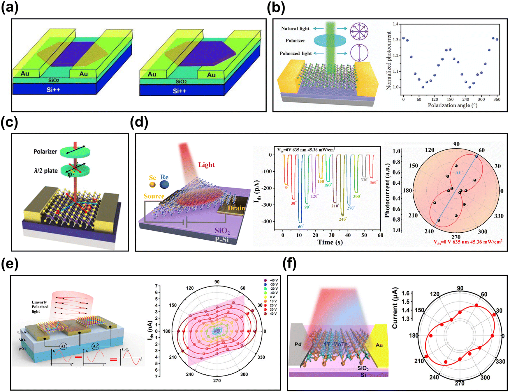 | ||
| Fig. 2 (a) Schematic illustration of two kinds of single micrometer-sized GeSe nanosheet-based device with top-contact and bottom-top-contact. Reproduced with permission.100 Copyright 2012, WILEY-VCH Verlag GmbH & Co. KGaA. (b) Schematic structure of GeSe-based photodetector and the normalized photocurrent as a function of polarization angle. Reproduced with permission.79 Copyright 2018, WILEY-VCH Verlag GmbH & Co. KGaA. (c) Schematic diagram of a ReSe2 device structure. Reproduced with permission.101 Copyright 2016, American Chemical Society. (d) 3D schematic image of the 2D ReSe2 Schottky photodetector with geometry-asymmetric contacts on symmetric Au electrodes, time-resolved self-powered photocurrent curves under different polarization angles and polar plot of the photocurrent at different polarization angles. Reproduced with permission.51 Copyright 2024, American Chemical Society. (e) Schematic diagram of a balanced ReS2 device structure and Polar plot of the photocurrent response measured at different gate voltages. Reproduced with permission.84 Copyright 2024, Wiley-VCH GmbH. (f) Schematic diagram of a 1T′-MoTe2 device and polar plot of the photocurrent at different polarization angles. Reproduced with permission.85 Copyright 2023, American Chemical Society. | ||
While some polarization-sensitive photodetectors based on 2D GeSe have been reported, in-plane optical anisotropy of GeSe was not the focus of research at that time. In 2019, Yang et al.102 systematically studied the in-plane optical anisotropy of GeSe, including its anisotropic light absorption, reflection, extinction and refraction. By using angle-resolved photoemission spectroscopy for the first time, they experimentally observed the anisotropic band structure of GeSe and interpreted the origin of its optical anisotropy. This research effectively stimulated the exploration of GeSe in polarization-sensitive photodetectors and provided basic information on the optical anisotropy of GeSe. In recent years, people are no longer satisfied with just relying on the intrinsic in-plane anisotropy of GeSe to detect polarized light. He et al.80 reported a polarization-sensitive photodetector based on GeSe with photoinduced short-wave infrared detection. By inducing Ge vacancies in GeSe through illumination, the photoresponse range of GeSe photodetector has been widened from the visible light to 1600 nm. For the first time, polarization-sensitive photoresponse was achieved at 1310 nm and 1550 nm (sub-waveband radiation), realizing infrared polarization-sensitive photoresponse in GeSe. The validity of the experimental method was also verified using GeS. This study not only provided guidance for the exploration of GeSe, but also offered great reference value for the research of other 2D materials in polarization-sensitive photodetectors.
Additionally, group VII transition metal dichalcogenides (TMDs) like 2D ReSe2 and ReS2 have also garnered significant research attention. Their photoresponse ranges span the visible light and near-infrared ranges. Due to their distorted octahedral symmetrical structure, they present good linear polarization sensitivity, making them suitable for application in polarization-sensitive photodetectors. In 2016, Zhang et al.101 first reported a photodetector based on 2D ReSe2 nanosheet (Fig. 2c). They synthesized ReSe2 nanosheets using chemical vapor deposition (CVD) method. The top-gated field effect transistor (FET) device based on ReSe2 achieved a maximum Ion/Ioff ratio of 107. They then performed gate modulation control on the devices using SiO2 and h-BN as gate dielectrics, respectively. It was found that the carrier mobility could be increased by more than 500 times when using an h-BN dielectric layer. They applied photocurrent mapping to investigate the polarized characteristics of ReSe2 devices under gate voltage modulation, providing guidance for subsequent research on ReSe2 polarization-sensitive photodetectors. Mathew et al.103 in 2022 also synthesized ReSe2 nanosheets using the CVD method. They then fabricated a light-emitting transistor (LET) using asymmetric platinum (Pt)/chromium (Cr) electrodes. Due to the asymmetric electrodes, it achieved balanced electron–hole densities and field-effect mobility, thereby realizing a low turn-on voltage device. The device stably emitted polarization-related near-infrared spectra at room temperature. It provided a very effective reference for future realization of infrared polarization light detection based on ReSe2. Just this year, Liu and Zheng et al.82 constructed a series of 2D ReSe2 Schottky photodetectors with geometrically asymmetric contacts. Due to differences in Schottky barrier heights caused by the asymmetry in contact area, interface states, and thickness variations, these devices exhibited impressive optoresponse performance and polarization sensitivity in self-power mode. Fig. 2d illustrates the schematic diagram of the device structure and the polarization-sensitive photocurrent under 635 nm laser illumination in self-power mode. The device achieved PR of 3.1 and 3.6 under 635 nm and 808 nm lasers, respectively. Its outstanding imaging capabilities were also demonstrated. This work reveals the enormous potential of ReSe2 Schottky photodetectors with geometrically asymmetric contacts in high-performance, self-powered, and polarization-sensitive photodetection.
Also in 2016, Liu et al.104 first reported a broadband polarization-sensitive photodetector based on few-layer ReS2. Since then, people began to realize the huge potential of ReS2 in the field of polarized light detection. Lin et al.83 vertically stacked two independent ReS2 nanobelt devices at an angle of 60° to construct a linear polarization polarimeter that can distinguish the linear polarization state of incident light in the 590 to 800 nm range. The single ReS2 device also achieved a PR of up to 1.72 at 665 nm and had an ultra-high responsivity of 959 A W−1. This provided reference for subsequent fabrication of high-performance ReS2 devices. Hu et al.84 proposed a balanced photodetector based on 2D ReS2 this year, which exhibited good polarization anisotropy (Fig. 2e). The device consists of two photodetectors of ReS2 that are perpendicular to each other in crystal orientation. A single device can show a PR of 2.79 under 650 nm laser irradiation. When the two devices are combined together due to their vertical orientation in crystal, their sensitivity to polarized light can be enhanced by more than two orders of magnitude. This work provides a new approach for further developing 2D polarization-sensitive photodetectors.
The response range of early introduced 2D materials mainly focused on the visible light band. Although some methods can realize the detection of ultraviolet or infrared polarized light, the effect is not satisfactory. Researchers started to explore low bandgap 2D materials to pursue polarization light detection in the infrared band. As is well known, MoTe2 is an excellent TMD material. But when it transforms from the 2H phase to the 1T′ phase similar to ReSe2 and ReS2, it exhibits stronger spin–orbit coupling and ferromagnetism, and has semimetal properties (with a small bandgap when single-layer or few-layer, and the bandgap gradually disappears as the thickness increases). In 2016, Beams et al.105 first systematically studied the structural characteristics of 1T′-MoTe2 with different layer numbers, revealing its strong optical anisotropy caused by structural asymmetry. Subsequently, in 2019, Zhu et al.106 experimentally obtained the birefringent refractive indices of few-layer 1T′-MoTe2. These studies provided indispensable fundamentals for the subsequent exploration of polarization-sensitive photodetectors based on 1T′-MoTe2. In 2023, Mao et al.85 synthesized wafer-scale (1 inch) few-layer 1T′-MoTe2 using an improved chemical vapor deposition method with precursor predeposition. They fabricated asymmetric Pd/Au electrodes photodetectors. Fig. 2f shows the schematic diagram of the device structure and the polarization plot of the polarization-sensitive photocurrent. Even when expanded to 1200 nm, the device still maintains high performance, with a PR of 1.2. This study provides inspiration for the future large-scale application of 1T′-MoTe2 in polarization-sensitive photodetectors.
In addition, the other semimetal 2D material PdSe2 also presents potential in polarization-sensitive photodetectors. PdSe2 shows a unique pentagonal structure, which endows it with some unique optical, electrical and thermoelectric properties. Excellent carrier mobility and strong in-plane anisotropy have made it a darling in polarization-sensitive photodetector research in recent years. Liang et al.107 reported a polarization-sensitive photodetector based on 2D PdSe2, which had an ultra-high responsivity of 708 A W−1 in 1064 nm and experimentally determined the optical polarization anisotropy of PdSe2. The device schematic diagram and polarization-sensitive photocurrent plot are shown in Fig. 3a. Zhong et al.45 fabricated polarization-sensitive photodetectors using mechanically exfoliated PdSe2 and verified its strong anisotropy through polarization-resolved absorption spectra measurements. Jiang et al.88 constructed a lateral PdSe2 p–i–n homojunction photodetector through electrostatic doping, and verified its polarization distinction capability (PR = 1.6) in the near-infrared range (1064 nm). Fig. 3b shows the schematic structure diagram of the device and the polarization-sensitive photocurrent plot. The device demonstrated excellent performance (R = 1.1 A W−1, D* = 1.3 × 10¹¹ Jones) at 1064 nm, providing potential guidance for fabricating next-generation high-performance polarization-sensitive photodetectors. In addition, the photo-thermoelectric effect of PdSe2 was also revealed. Li et al.86 demonstrated a PdSe2 photodetector grown by CVD, verifying that the current was from the temperature difference caused by the laser irradiation, confirming the existence of the photo-thermoelectric effect in PdSe2. It also demonstrated the polarization light detection capability (PR = 1.3) of the device under the photo-thermoelectric effect. Dai et al.87 made full use of the photo-thermoelectric effect of PdSe2, successfully extending the detection band of the2D PdSe2-based photodetector to 10.5 μm. They fabricated a PdSe2 device using asymmetrical electrodes of multilayer graphene and Au, with a large difference in thermal conductivity between the two electrodes, which could effectively increase the temperature difference in the channel caused by the laser irradiation. This helped it achieve PR values of 2.06 and 1.21 at 4.6 μm and 10.5 μm, respectively. This research provides powerful guidance for the development of 2D PdSe2 in the field of infrared polarization-sensitive photodetection based on the photo-thermoelectric effect.
 | ||
| Fig. 3 (a) Schematic diagram of the PdSe2-based photodetector and polar plot of photocurrent variation with polarization angle. Reproduced with permission.107 Copyright 2019, WILEY-VCH Verlag GmbH & Co. KGaA. (b) Schematic illustration of the device, schematic cross-sectional illustration of the doping distribution and polar plots of the photocurrent as a function of polarization angle. Reproduced with permission.88 Copyright 2023, American Chemical Society. (c) Schematic illustration of the polarization dependent photoresponse measurements of Te nanowire device arrays and time-resolved photoresponse recorded with light polarization direction changing from 0 to 360°. Reproduced with permission.90 Copyright 2023, Wiley-VCH GmbH. (d) Schematic representation of the GeAs2 polarization-sensitive photodetector and polar plot of the normalized polarization-dependent photocurrent (red square) and reflectance contrast (green circle). Reproduced with permission.108 Copyright 2018, WILEY-VCH Verlag GmbH & Co. KGaA. (e) The schematic of polarization-sensitive 2D t-InTe-based photodetector and polarization angle-dependent time-resolved photoresponse curves. Reproduced with permission.91 Copyright 2024, Wiley-VCH GmbH. (f) Schematic diagram of GeS2 photodetector and polar plot of photocurrents under different polarization angle of incident light. Reproduced with permission.39 Copyright 2019, WILEY-VCH Verlag GmbH & Co. KGaA. | ||
In a creative spirit, researchers have consciously synthesized 2D materials with asymmetric structures to advance the development of 2D polarization-sensitive photodetectors. This approach leverages their unique structural characteristics for enhanced polarized light detection. Tellurium (Te), an elemental 2D semiconductor featuring a quasi-1D crystal structure, exhibits anisotropic physical properties, making it a particularly popular 2D material in recent years. Wei et al.90 induced the directional epitaxial growth of quasi-1D Te nanowires through physical vapor deposition in nano-grooves on annealed m-plane sapphire. The resulting Te-based photodetector demonstrated a broadband response ranging from 532 nm to 2530 nm and achieved polarization-sensitive infrared light detection (PR = 2.05 at 1550 nm). The device structure and time-resolved photocurrent at different polarization angles are shown in Fig. 3c. Li et al.108 synthesized single crystal GeAs2 through chemical vapor transport (CVT) and conducted a comprehensive study of its structure, vibration, electrical properties, and in-plane optical anisotropy. The few-layer GeAs2-based polarization-sensitive photodetector exhibited anisotropic photodetection capacity (Fig. 3d), with a PR can reach 2, sparking interest in the development of IV–V compounds. Zhou et al.91 first prepared large-area tetragonal (t-) InTe nanosheets using CVD. Due to its inherent narrow bandgap (1.28 eV) and low symmetry, the 2D t-InTe photodetector demonstrated a PR of 1.81 at near-infrared band (808 nm), surpassing most 2D anisotropic materials. The schematic diagram of the device structure and time-resolved photocurrent at different polarization angles are shown in Fig. 3e. Yang et al.39 reported an ultraviolet polarization-sensitive photodetector based on 2D GeS2 (Fig. 3f), addressing the gap in 2D polarization-sensitive photodetectors within the ultraviolet range. With a bandgap greater than 3 eV, GeS2 can effectively detect light in the ultraviolet range. Additionally, its intrinsic structural asymmetry enables a PR of 2.1 in the ultraviolet range. This work provides valuable guidance for exploring polarized light detection in the ultraviolet spectrum. Zhao et al.89 demonstrated a polarization-sensitive photodetector based on 2D SiP, as shown in Fig. 4a. Due to the intrinsic structural properties of SiP, this device achieves a fast response time of 30 microseconds and a PR up to 2.9. Recently, Liu et al.92 conducted a study on a polarization-sensitive photodetector utilizing 2D violet phosphorene (VP), which possesses an asymmetric structure similar to BP. Fig. 4b illustrates the schematic diagram of the device structure, along with its 2D colormap depicting the anisotropic photocurrent. The device exhibited a remarkable responsivity of up to 341 A W−1 and a PR of 3.9. These findings suggest a promising future for VP in the realm of 2D polarization-sensitive photodetection. Furthermore, Cheng et al.93 utilized density functional theory-based electronic density calculations to demonstrate the strong in-plane anisotropy of In2Te5. They subsequently developed a polarization-sensitive photodetector based on this material, which exhibited PR of 1.26 and 1.34 at 445 nm and 638 nm, respectively. This research has the potential to stimulate further exploration of III–IV group 2D materials (Pentatellurides M2Te5, where M = Al, Ga, In, etc.) for polarized light detection applications. Additionally, Guo et al.94 employed Bi2O3 powder and Bi2Se3 fragments as precursors and additives, respectively, and adopted a surface-assisted passivation growth strategy to synthesize 2D, ultra-thin β-Bi2O3 nanosheets. They subsequently developed a polarization-sensitive photodetector based on this material, which demonstrated a remarkable PR of 1.91 in the ultraviolet 365 nm wavelength range, and exhibited excellent ultraviolet polarization imaging capabilities. This work opens up new avenues for the synthesis of 2D materials with polarization-sensitive performance in the ultraviolet spectral region.
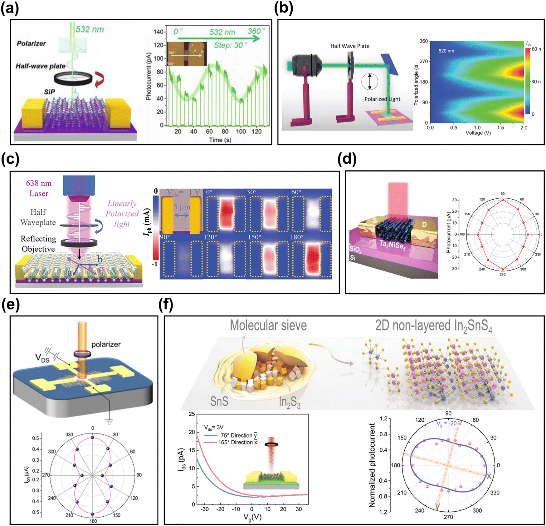 | ||
| Fig. 4 (a) Schematic representation of the polarization-sensitive photodetector based on SiP flake and time-resolved photoresponse with light polarization direction along 0–180° recorded under 532 nm laser sources. Reproduced with permission.89 Copyright 2021, Wiley-VCH GmbH. (b) Schematic representation of the polarization-sensitive photodetector based on the 2D VP nanosheet and 2D colormap of the anisotropic photocurrent of the photodetector. Reproduced with permission.92 Copyright 2023, Wiley-VCH GmbH. (c) A diagrammatic illustration of nanoflake-based polarization-sensitive photodetectors utilizing Ta2NiSe5 material and photocurrent mapping obtained by scanning photodetectors under the 638 nm laser with the polarized angle varying from 0° to 180°. Reproduced with permission.95 Copyright 2023, Wiley-VCH GmbH. (d) Schematic diagram of the Ta2NiSe5 photodetector device and anisotropic photocurrent under 1550 nm laser illumination. Reproduced with permission.97 Copyright 2021, Elsevier Ltd. (e) Schematic diagram of the angle-resolved polarization-sensitive photoresponse measurement setup and anisotropic photocurrent for the linear polarized lasers at 400 nm. Reproduced with permission.96 Copyright 2021, American Chemical Society. (f) Schematic diagram of synergistic additive of salt and molecular sieve-assisted CVD growth process, the transfer characteristics of the device along the x and y directions at Vds = 3 V and normalized Iph as a function of polarization angle. Reproduced with permission.99 Copyright 2021, Wiley-VCH GmbH. | ||
In recent years, ternary materials have garnered significant attention from researchers due to their asymmetric structures and unique properties. Ta2NiSe5 is a representative example. Both experimental and theoretical investigations have established that it possesses a bandgap of 0.36 eV at room temperature, which exhibits minimal dependence on thickness.109 This narrow bandgap enables it to interact with light in the far infrared range. Furthermore, as a ternary compound, Ta2NiSe5 offers the advantage of tuning its electronic and optoelectronic properties through stoichiometric variations, thereby providing greater flexibility. Its inherent in-plane anisotropy also renders it an ideal candidate for broadband polarization photodetection. Zhang's team95 demonstrated an h-BN-encapsulated Ta2NiSe5 polarization-sensitive photodetector with a working wavelength spanning from 520 nm to 4.6 μm. Their work systematically evaluated the polarization-sensitive photoresponse at 638 nm (Fig. 4c). Due to the intrinsic structural properties of Ta2NiSe5, the photodetector exhibited considerable polarized light detection capability. However, the study did not explore polarization-sensitive photodetection in the infrared range. Zhang et al.97 utilized the CVT method to prepare Ta2NiSe5 nanosheets. The resultant photodetector exhibited a broadband photoresponse ranging from 405 nm to 4.6 μm. Fig. 4d illustrates the device schematic and photocurrent polarization plot under 1550 nm light, achieving a PR of 1.46, realizing effective exploration of infrared polarized light detection capability of Ta2NiSe5. Qiao et al.96 also studied Ta2NiSe5 grown via the CVT method, systematically examining its anisotropic electronic transport and optoelectronic properties. The Ta2NiSe5-based photodetector achieved a maximum PR of 3.24 at 1064 nm (Fig. 4e). This research contributes to the understanding and development of applications involving in-plane anisotropic 2D materials in photodetectors. Additionally, Zhai's group98 synthesized 2.4 nm thick PbSnS2 nanosheets using the CVD method and systematically investigated its anisotropic optical and electrical properties. Zuo et al.99 employed the same method to synthesize 2D In2SnS4 nanosheets and achieved control over its anisotropy through gate voltage modulation. Fig. 4f depicts the schematic diagram of material growth, transfer curve characteristics of the device along different directions, and normalized photocurrent as a function of polarization angle. The In2SnS4 device exhibited a maximum PR of 1.70 at a gate voltage of −20 V. This research not only offers insights into the synthesis of ternary materials but also provides an effective method for modulating the polarization-sensitive photoresponse.
4. Polarization-sensitive photodetectors based on 2D material heterostructures
While polarization-sensitive photodetectors based on single 2D materials have demonstrated impressive performance, various methods have been attempted to further enhance their polarization sensitivity. Among these, heterogeneous structure engineering stands out as the most promising strategy. This approach leverages the exceptional properties of different materials and may uncover novel mechanisms. Consequently, it offers an effective pathway to achieving high-performance polarization-sensitive photodetectors. In this section, we review the recent advancements in polarization-sensitive photodetectors based on 2D vdWs heterojunctions. Table 3 provides a comparison of the performance of polarization-sensitive photodetectors utilizing 2D vdWs heterojunctions. To facilitate a comprehensive understanding of their working principles, we classify these photodetectors into three categories: type-I band alignment, type-II band alignment, type-III band alignment and Schottky band alignment, as depicted in Fig. 5.| Materials | Wavelength (nm) | R (A W−1) | D* (Jones) | τ rise/τfall (ms) | PR | Ref. |
|---|---|---|---|---|---|---|
| GeS2/PbSe | 1300 | 320 | 1012 | — | 3.36 | 110 |
| Gr/2H-MoTe2/BP | 1310 | 0.17 | 2 × 10⁹ | — | 6 | 111 |
| Te/MoSe2 | 405 | 2.106 | 2.91 × 10¹³ | 22/25 | 16.39 | 47 |
| WSe2/Ta2NiSe5 | 780 | 22![[thin space (1/6-em)]](https://www.rsc.org/images/entities/char_2009.gif) 000 000 |
2 × 10¹² | 0.0018 | 1.35 | 33 |
| WSe2/Ta2NiSe5 | 532 | 0.034 | 1.08 × 10¹⁰ | 0.094/0.091 | 3.84 | 112 |
| WSe2/Te | 405 | 402 | 9.28 × 10¹³ | 1.7/3.2 | 2.5 | 30 |
| 2H-MoTe2/Ta2NiSe5/Gr | 2200 | 5.79 | 1010 | — | 1.44 | 52 |
| 2H-MoTe2/As0.4P0.6 | 405 | 1590 | 1.2 × 10¹² | 0.025/0.03 | 10 | 50 |
| GeAs/InSe | 635 | 0.357 | 2 × 10¹¹ | 25/25 | 18 | 113 |
| GeAs/WS2 | 635 | 0.509 | 1.08 × 10¹² | 1.5/1.3 | — | 114 |
| 1310 | — | — | — | 4.5 | ||
| 1550 | — | — | — | 3.1 | ||
| MoSe2/GeSe/MoSe2 | 635 | 0.22 | 6.6 × 10¹⁰ | — | 12.5 | 38 |
| β-In2Se3/Te | 1310 | 2 | 2.14 × 10⁹ | 0.49/0.51 | 4.95 | 115 |
| MoS2/GaAs | 780 | 0.0352 | 1.96 × 10¹³ | 0.0034/0.0156 | 4.8 | 116 |
| 2H-MoTe2/Ta2NiSe5/2H-MoTe2 | 635 | 0.06 | 4 × 10¹² | 0.0035/0.0042 | 16.3 | 117 |
| 1550 | — | — | — | 8.1 | ||
| ReSe2/ReS2 | 350 | 126.56 | 3.16 × 10¹¹ | 0.006/0.0089 | — | 118 |
| 638 | 16.24 | 4.06 × 10¹⁰ | — | 1.2 | ||
| 980 | 0.66 | 1.66 × 10⁹ | — | 2.0 | ||
| VP/InSe | 1064 | 182.8 | 7.86 × 10¹² | — | — | 53 |
| VP/Gr/InSe | 1064 | 230 | 4.64 × 10¹³ | 0.017/0.018 | 2.59 | |
| ReSe2/WSe2 | 638 | 0.57 | 1010 | 0.002/0.0025 | 2 | 46 |
| WSe2/Ta2NiSe5/WSe2 | 635 | 0.436 | 1.0 × 10¹² | 0.42/0.64 | 13.9 | 51 |
| ReSe2/SnSe2 | 635 | 0.096 | 1 × 10¹⁰ | 0.996/1.42 | 12.26 | 36 |
| ReSe2/MoS2 | 635 | 0.011 | 1 × 10⁹ | 270/320 | 5.1 | |
| Gr/ReSe2/SnSe2 | 635 | 0.144 | 2.4 × 10¹⁰ | 0.752/0.928 | 13.27 | |
| Rubrene/WS2 | 405 | 227 | 4 × 10¹¹ | 0.18/0.21 | 1.5 | 119 |
| 2H-MoTe2/GeSe/MoS2 | 635 | 0.732 | 2.3 × 10¹² | 17.06/21.41 | 11.2 | 120 |
| ReSe2/MoS2 | 638 | 3.52 | 1011 | 5.0/9.1 | 1.35 | 49 |
| 2H-MoTe2/1T′-MoTe2/MoSe2 | 1310 | 0.76 | 3 × 10⁹ | 13/10 | 55 | 121 |
| 1T′-MoTe2/MoS2 | 915 | 0.079 | 1.2 × 10¹⁰ | 0.18/0.202 | 1.98 | 122 |
| 1T′-MoTe2/WS2 | 635 | 2.04 | 1.2 × 10¹² | 0.045/0.049 | 5 | 123 |
| 1T′-MoTe2/WS2/1T′ -MoTe2 | 635 | 1.06 | 5.6 × 10¹¹ | 0.048/0.048 | 13 | |
| Gr/PdSe2/Ge | 980 | 0.691 | 1.73 × 10¹³ | 0.006/0.092 | 91.2 | 40 |
| PdSe2/CdTe | 780 | 0.324 | 3.3 × 10¹² | 0.0049/0.0083 | 4.4 | 124 |
| PdSe2/GaN | 360 | 0.249 | 7.9 × 10¹² | 0.028/0.122 | 4.5 | 48 |
| PdSe2/Si | 980 | 0.726 | 3.19 × 10¹⁴ | 0.025/0.034 | 75 | 44 |
| PdSe2/Te | 1550 | 0.617 | 5.27 × 10¹⁰ | 0.005/0.004 | 3.56 | 125 |
 | ||
| Fig. 5 Schematic diagram of four heterojunction band alignments. | ||
Band alignment in 2D vdWs heterojunctions has been a subject of extensive discussion. When 2D semiconductors form vdWs heterojunctions, there are three possible types of band alignments: type-I, type-II, and type-III. However, the separation of bands in type-III structures hinders the recycling and utilization of photo-generated carriers at the interface, significantly impacting photoelectric conversion efficiency. Additionally, photodetectors with type-III band alignment are prone to uncontrollable internal electric field effects during operation, potentially influencing photoresponse. From a material integration perspective, the separated energy bands make it challenging to effectively combine the optical or electrical properties of the constituent materials. Consequently, research on type-III band alignment remains relatively sparse, except for specific applications such as band-to-band transitions. Due to the rarity of type-III band heterojunction structures, this reiew focuses solely on analyzing type-I and type-II band alignments in 2D semiconductor heterojunctions.
4.1 Polarization-sensitive photodetectors based on 2D heterostructures with type-I band alignment
Type-I band alignment typically occurs in heterojunctions where one component possesses a narrower bandgap. Well-designed 2D heterostructures featuring type-I band alignment are more stable and exhibit superior integration of optical and electrical properties compared to type-II band alignment.126 Recently, our team reported a polarization-sensitive photodetector based on a WS2/Te type-I band heterojunction.30 This device demonstrated exceptional performance, including a responsivity of 405 A W−1, a detectivity of 9.28 × 10¹³ Jones, rapid rising and falling times of 1.7 ms and 3.2 ms, respectively, and a PR of 2.5. Furthermore, it was successfully integrated into a polarization-sensitive imaging system. Fig. 6a illustrates the schematic diagram of the device and the polarization-sensitive imaging results. These remarkable performances, particularly the anisotropic properties, were significantly enhanced compared to previously reported single Te-based devices, highlighting the superiority of type-I band heterojunctions in polarization-sensitive photodetection. Additionally, Zhao et al.47 reported an outstanding MoSe2/Te type-I band heterojunction polarization-sensitive photodetector. Fig. 6b displays the device schematic and polarization-sensitive photocurrent plot. This device exhibited a PR of 16.39 in self-driving mode, approximately one order of magnitude higher than that of single Te-based devices. This substantial enhancement can be attributed to the high quality of Te nanoflakes prepared by the solution synthesis method and the effective utilization of electrons under type-I band alignment. Apart from Te, BP, another narrow-bandgap 2D material, has been extensively studied for its anisotropy. Recently, there have been novel approaches to utilizing BP. Shen et al.111 described a gate-tunable polarization-sensitive photodetector based on BP. This device employed a vertical Gr/2H-MoTe2/BP heterostructure as the light-active layer on a sapphire (Al2O3) substrate, with an h-BN dielectric layer. The device effectively detected infrared (1550 nm) polarized light and achieved polarization reversal in both visible light (638 nm) and infrared light (1550 nm) by tuning the gate voltage. This research offers new insights into narrow-bandgap 2D materials, significantly advancing their development in the field of polarization-sensitive photodetectors.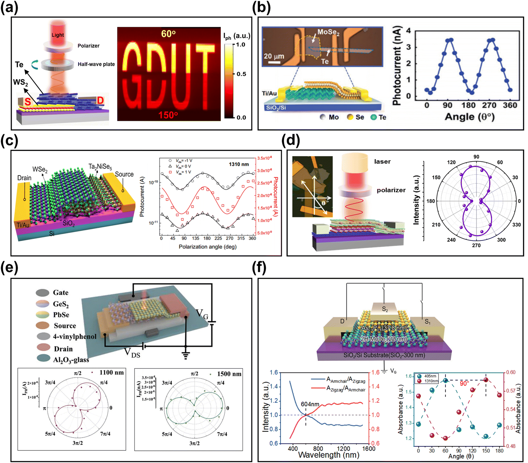 | ||
| Fig. 6 (a) Schematic diagram of the polarization-sensitive photodetection measurement and polarization imaging diagram. Reproduced with permission.30 Copyright 2023, Wiley-VCH GmbH. (b) Optical microscope image and schematic diagram of a MoSe2/Te device structure and polarization-sensitive photocurrent for the incident wavelengths of 405 nm. Reproduced with permission.47 Copyright 2021. The Royal Society of Chemistry. (c) Schematic diagram of a WSe2/Ta2NiSe5 device structure and testing of polarization-sensitive photocurrent of the device at different voltages under 1310 nm light. Reproduced with permission.33 Copyright 2024, Nature Publishing Group. (d) Schematic diagram of a Gr/Ta2NiSe5/2H-MoTe2 device structure and polarization-sensitive photocurrent polarization diagram. Reproduced with permission.52 Copyright 2024, Wiley-VCH GmbH. (e) Schematic diagram of the heterostructure device and the polar plots of the relationship between photocurrent and polarization angle under 1100 nm and 1500 nm light, respectively. Reproduced with permission.110 Copyright 2024, Wiley-VCH GmbH. (f) Schematic diagram of a 2H-MoTe2/As0.4P0.6 device structure, wavelength-dependent photocurrent testing graph of the device and polarization-sensitive light absorption testing diagrams at 405 nm and 1310 nm respectively. Reproduced with permission.50 Copyright 2023, Wiley-VCH GmbH. | ||
In the preceding section, Ta2NiSe5, a narrow-bandgap 2D material, was highlighted, having gained significant popularity in recent years. Its distinctive structural attributes render it highly favored for use in single-material polarization-sensitive photodetectors and equally appealing for constructing vdW heterostructures. Liu et al.33 presented a WSe2/Ta2NiSe5 type-I band heterojunction photodetector (depicted in Fig. 6c), where tunneling facilitated by photogating enhanced both the responsivity and response speed of the device concurrently. Additionally, they revealed that under an electric field, photogating-assisted tunneling enabled carrier multiplication and acceleration. This device also exhibited tunable PR that was wavelength-dependent, offering valuable insights for wavelength identification. The operational principle of this device hinges on the photogating effect, primarily attributed to the photo-induced gate voltage generated by trap states resulting from confined electrons or holes.59 The contribution of the type-I band structure is indispensable here, as it facilitates the trapping of carriers under light illumination, leading to the formation of trap states and subsequently photo-induced gating to assist tunneling. Simultaneously, Zhu et al.112 demonstrated another promising application of the WSe2/Ta2NiSe5 vdW heterojunction as a polarization-sensitive photodetector. In self-driving mode, the device achieved a high detectivity of 1.08 × 10¹⁰ Jones and an ultra-fast response time of merely 91 μs. Moreover, owing to the intrinsic structural anisotropy of Ta2NiSe5, the device possessed robust polarization-sensitive photodetection and high-resolution polarization-sensitive imaging capabilities. Leveraging these features, the device facilitated the realization of multimode optoelectronic logic gates through the co-modulation of light′s on/off state, polarization angle, gate voltage, and bias voltage. This research offers significant theoretical and technical support for the advancement of multifunctional optoelectronic devices. Recently, our team reported a high-performance polarization-sensitive photodetector (Fig. 6d) based on Ta2NiSe5.52 We constructed a three-layer vdW heterostructure comprising Ta2NiSe5, 2H-MoTe2, and Gr. Under light illumination, a substantial number of polarization-sensitive carriers were generated in the top Ta2NiSe5 layer, swiftly separated by the middle 2H-MoTe2 layer, and efficiently collected by the bottom Gr layer. This device successfully detected polarized light ranging from 520 nm to 2200 nm and demonstrated high-resolution polarization-sensitive imaging capabilities. The type-I band alignment between Ta2NiSe5 and 2H-MoTe2 facilitated rapid carrier transfer. This work provides invaluable insights for exploring infrared polarization-sensitive imaging technologies.
Thus far, the exploration of application perspectives for 2D polarization-sensitive photodetectors has been constrained, and the number of reported 2D semiconductor materials exhibiting anisotropy remains relatively limited. Consequently, it is particularly crucial to explore novel applications for polarization-sensitive photodetectors and to identify new 2D anisotropic semiconductor materials. Liu et al.110 described an optoelectronic transistor based on a GeS2/PbSe vdWs heterojunction, which exhibits precise narrowband selective spectral detection (accuracy of 96.7%) in the short-wave infrared (SWIR) range and has high in-plane anisotropy and electrical reconfigurability. Fig. 6e shows the schematic diagram of the heterostructure device and the polar plots of the relationship between photocurrent and polarization angle under 1100 nm and 1500 nm light, respectively. The device also demonstrated deep learning analysis in combination with artificial neural networks. This paves the way for exploring new applications of 2D devices in this field in the future. Li et al.50 constructed a vdWs heterojunction using As0.4P0.6 with in-plane anisotropic structure and 2H-MoTe2, realizing a reconfigurable wide spectral band polarization-sensitive photodetector. As0.4P0.6 is a very promising 2D anisotropic material, but has been mentioned very little in previous studies. This device can achieve wide spectral band polarized light detection from 405 nm to 1550 nm, and has a high responsivity of 1590 A W−1 at 405 nm. Due to the wavelength-dependent polarization reversal characteristics of the As0.4P0.6 nanosheets, polarization reversal can be observed in both light absorption and photocurrent of the device (Fig. 6e). The detection mode can also be reconfigured from polarization-independence to polarization-susceptibility by changing the gate voltage. Many of these characteristics originate from the intrinsic structural properties of As0.4P0.6. This work introduces another very promising material for exploring 2D polarization-sensitive photodetectors and paves the way for realizing multifunctional polarization-sensitive photodetectors.
4.2 Polarization-sensitive photodetectors based on 2D heterostructures with type-II band alignment
Compared with type-I band alignment, type-II band alignment is more common in 2D optoelectronic detectors. The type-II band structure can more effectively utilize the photon energy. Electrons and holes can be separated in different materials, which can effectively reduce the recombination probability and achieve more complete separation. Moreover, the type-II band structure is easier to design and can provide more transition paths for carriers. Compared with type-I band alignment, it can more effectively realize performance enhancement of devices. In this section, we focus on some representative anisotropic materials and newly reported ones.Rhenium diselenide (ReSe2) and rhenium disulfide (ReS2), both group VII transition metal dichalcogenides introduced previously, are two typical examples. As early as 2018, Liu et al.127 employed a two-step epitaxial growth to synthesize large-area monolayer ReS2/ReSe2 lateral heterojunction. They observed polarization-sensitive photocurrent characteristics, demonstrating the linear polarization behavior in a 2D lateral heterostructure (Fig. 7a). However, they did not consider the lattice matching between the two anisotropic materials nor explore how to maximize the PR following their combination. Four years later, Li et al.118 prepared another ReSe2/ReS2 vdWs heterojunction polarization-sensitive photodetector by an alternating stacking method. This device successfully achieved high responsivity, wavelength-dependent bipolar photoresponse, ultrafast and polarization-sensitive photodetection capabilities. The device exhibited a positive response in the ultraviolet to visible spectral range and a negative response above 760 nm. This research revealed the enormous potential of ReX2 (X = Se, S) vdWs heterostructures in multifunctional polarization-sensitive photodetection. However, the study found that the stacking method weakened the linear polarization sensitivity of the ReSe2/ReS2 device, but did not alter the stacking method to improve the polarization sensitivity of the device. In the same year, the research group constructed a polarization-sensitive photodetector based on a ReSe2/MoS2 vdWs heterojunction using the same device structure.49 Its detection spectrum was no longer limited by the carrier mobility and bandgap of ReX2 that are independent of the number of layers. This device successfully realized polarized light detection up to the near-infrared band (1250 nm) using the same device structure. By replacing the material system from ReX2 to ReSe2/MoS2, the detector's spectral range was expanded without those limitations of intrinsic properties of ReX2.
 | ||
| Fig. 7 (a) Schematic diagram of a horizontal ReSe2/ReS2 heterojunction device structure, optical microscope image and polarization-sensitive photocurrent testing graph. Reproduced with permission.127 Copyright 2018, WILEY-VCH Verlag GmbH & Co. KGaA. (b) Schematic diagram of a Gr/ReSe2/SnSe2 device structure, optical microscope image and polarization-sensitive photocurrent polarization diagram. Reproduced with permission.36 Copyright 2024, Wiley-VCH GmbH. (c) Schematic diagram of a semi-vertical WSe2/ReSe2 heterojunction device structure, optical microscope image, band alignment diagram and polarization-sensitive photocurrent mapping diagram. Reproduced with permission.46 Copyright 2021, American Chemical Society. (d) Schematic diagram of a MoSe2/GeSe/MoSe2 device structure, polarization-sensitive photocurrent polarization diagram and polarization-sensitive photocurrent time-resolved curve. Reproduced with permission.38 Copyright 2024, Wiley-VCH GmbH. (e) Schematic diagram of a MoS2/GeSe/2H-MoTe2 device structure, polarization-sensitive photocurrent time-resolved curve and polarization diagram. Reproduced with permission.120 Copyright 2024, WILEY-VCH GmbH. | ||
Recently, Pan et al.36 demonstrated three polarization-sensitive photodetectors based on ReSe2 vdWs heterojunctions at once using a vertical stacking approach. They respectively fabricated ReSe2/SnSe2, ReSe2/MoS2, and Gr/ReSe2/SnSe2 vdWs heterojunction photodetectors and systematically studied and compared their optoelectronic properties. It was found that combining Gr with ReSe2/SnSe2 can increase the PR of the device by more than four times. The schematic and polarization-sensitive photocurrent at polar plot of the Gr/ReSe2/SnSe2 device are shown in Fig. 7b, which can be attributed to the synergetic effect of unilateral depletion and photoinduced tunneling mechanism after adding a few layers of Gr. In addition, the application capabilities demonstrated, such as clear and stable quaternary logic state polarization imaging without any power supply and excellent polarization modulation for optical communication, inject vitality into the development of 2D polarization-sensitive photodetectors. Fig. 7c shows a WSe2/ReSe2 heterojunction photodetector with a semi-vertical geometry and its mapping graph of polarization-sensitive photocurrent.46 It has a standard type-II band alignment with its main working wavelength at 980 nm in the near infrared. Additionally, the device demonstrated digital incoherent holographic 3D imaging in a self-driven mode, providing new reference for future applications of 2D polarization-sensitive photodetectors. Ahn et al.128 also demonstrated a polarization-sensitive photodetector based on a 2D ReS2/2H-MoTe2 vdWs heterojunction. It can respond to near-infrared light up to 1310 nm and realize polarized light detection. Moreover, using Pt and Ti/Au as electrodes at the two ends respectively, this device achieves a rectification ratio of four orders of magnitude.
This year, two different research groups consecutively reported on high-performance polarization-sensitive photodetectors utilizing vdWs heterostructures based on 2D GeSe. In their work, An et al.38 demonstrated polarization-sensitive photodetectors utilizing MoSe2/GeSe bilayer and MoSe2/GeSe/MoSe2 trilayer vdWs heterostructures. They primarily focused on the polarization-sensitive photoresponse of these devices under 635 nm laser illumination in self-driving mode. As illustrated in Fig. 7d, the MoSe2/GeSe/MoSe2 device exhibited a significant PR of 12.5, which is 3.5 times higher than that of the MoSe2/GeSe device and five times higher than that of the single GeSe device. Another trilayer heterostructure device employing the 2H-MoTe2/GeSe/MoS2 structure demonstrated ultra-strong antibipolar transfer characteristics through the incorporation of GeSe.120 This structure holds significant potential for applications such as frequency doubling and binary phase shift keying units in the communication field. Under self-driving mode operation at 635 nm, the device exhibited a PR of 11.2, as shown in Fig. 7e. Comparative testing further verified that the anisotropy of its photocurrent originates from the structural characteristics of GeSe. In addition to GeSe, Huo's team demonstrated two polarization-sensitive photodetectors based on 2D vdWs heterostructures of GeAs/WS2 and GeAs/InSe.113,114 Their polarization performance was attributed to GeAs, which exhibits classic type-II band alignment, enabling high responsivities of 509 mA W−1 and 357 mA W−1 for the GeAs/WS2 and GeAs/InSe devices, respectively, at 635 nm. Furthermore, due to the narrow bandgap (0.83 eV) of GeAs, the GeAs/WS2 device achieved PR values of 4.5 and 3.1 at short-wave infrared wavelengths of 1310 nm and 1550 nm, respectively (Fig. 8a). Leveraging the high performance of InSe, the GeAs/InSe device fully exploited their performance advantages, achieving a PR of 18 at 635 nm in self-driving mode (Fig. 8b), surpassing most 2D polarization-sensitive photodetectors. This year, Huo's team also demonstrated a polarization-sensitive photodetector based on a 2D β-In2Se3/Te vertical vdWs heterostructure. Benefiting from the proven high performance of In2Se3 and the strong anisotropy of Te, this device exhibited high performance in the short-wave infrared region, with responsivities of 2 A W−1 at 1310 nm and 0.71 A W−1 at 1550 nm, and detectivities of 2.14 × 10⁹ Jones and 7.3 × 10⁸ Jones, respectively.129 Additionally, it demonstrated potential for polarization-sensitive imaging sensors. Fig. 8c shows the device schematic and polarization-sensitive photocurrent curve as well as polarization imaging at 1310 nm, and this device can also be used for infrared ASCII code communication transmission. These studies by Huo's team provide new opportunities to further explore 2D polarization-sensitive photodetectors.
 | ||
| Fig. 8 (a) The polarization sensitive photocurrent of the GeAs/WS2 device under 1310 nm and 1550 nm lasers with varying polarization angles. Reproduced with permission.114 Copyright 2022, American Chemical Society. (b) The time resolved photocurrent of GeAs/InSe heterojunction under polarized light with varying polarization angle from 0° to 330° under 635 nm and polarization sensitive photocurrent as a function of the polarization angle in the polar coordinates. Reproduced with permission.113 Copyright 2021, Wiley-VCH GmbH. (c) The schematic structure of the β-In2Se3/Te polarization-sensitive photodetector, the polarization-resolved photoresponse under 1310 nm and imaging patterns of the letters “Te” at 0° and 90°, respectively. Reproduced with permission.115 Copyright 2024, Wiley-VCH GmbH. (d) The schematic structure of the InSe/Gr/VP polarization-sensitive photodetector and angle-resolved photocurrent data. Reproduced with permission.53 Copyright 2024, American Chemical Society. (e) Schematic diagram of the Nb2GeTe4/MoS2 photodetector under the MIR light irradiation, atomic structure of Nb2GeTe4 and MoS2, optical image of the heterojunction and the linear polarization photoresponse of the heterostructure for the 3.7, 4.6, and 11.0 μm MIR light. Reproduced with permission.130 Copyright 2023, Wiley-VCH GmbH. | ||
Based on the preceding mentioned 2D anisotropic material VP, Ahmad et al.53 proposed a type-II VP/InSe vdWs heterostructure recently. Under 1064 nm light excitation, this device exhibited an R of 182.8 A W−1 and a D* of 7.86 × 10¹² Jones. Moreover, they found that inserting a few layers of Gr between VP and InSe can effectively enhance the photodetection performance (Fig. 8d). Due to the intrinsic in-plane anisotropy of VP, this device also showed a PR of 2.7. Zheng et al.119 proposed an organic/inorganic 2D vdWs heterostructure polarization-sensitive photodetector. By combining the organic single crystal rubrene with the 2D WS2, and leveraging the better carrier mobility, longer exciton diffusion length, anisotropic charge transport and unique linear dichroism of organic single crystals, the photodetection performance was extended, realizing an R of 1000 A W−1 and a response time of 180 μs. Additionally, a PR of 1.7 was achieved in the visible light region by utilizing the anisotropy of rubrene, providing very valuable reference for exploring new types of 2D polarization-sensitive photodetectors.
In recent years, ternary 2D tellurides materials including TaIrTe4, NbIrTe4, Nb2SiTe4 and Nb2GeTe4 have attracted attention due to their optical anisotropy, narrow bandgap and topological insulator properties, and they are considered potential candidates for far-infrared polarization-sensitive photodetection. Han et al.130 described a polarization-sensitive photodetector based on an Nb2GeTe4/MoS2 vdWs heterostructure, which covers a wide spectral range from 3.7 to 11 μm. Combining the clear photovoltaic effect in the heterojunction region and the bolometric effect of MoS2, this device achieved PR values of 48 and 34 under 4.6 μm and 11 μm light irradiation, respectively. Interestingly, under 3.7 μm light, the device exhibited a bipolar photoresponse, with PR showing −3.38 (Fig. 8e), which can be attributed to the bolometric effect of MoS2 leading to a negative dominant response at specific wavelengths. Based on these characteristics, this device has been successfully applied to bipolar infrared polarization coding communication and polarization imaging.
4.3 Polarization-sensitive photodetectors based on 2D Schottky heterostructures
The Schottky band alignment discussed in this section pertains specifically to vdWs heterojunctions comprising one or more 2D semimetal materials. Such heterojunctions typically exhibit pronounced photovoltaic effects, rendering them highly suitable for self-driving photodetectors characterized by ultra-fast response speeds. Over the past five years, 2D anisotropic semimetal materials, particularly 1T′-MoTe2 and PdSe2, have garnered significant attention. This section primarily reviews and summarizes the strengths and weaknesses of 1T′-MoTe2 and PdSe2 in Schottky vdWs heterojunction polarization-sensitive photodetectors reported in recent years. It is anticipated that this analysis will offer valuable insights for the future development of Schottky band alignment heterojunction photodetectors. Recently, Pan et al.34 demonstrated a polarization-sensitive photodetector based on a 2H-MoTe2/1T′-MoTe2/MoSe2 trilayer vdWs heterostructure. This photodetector exhibits a strong photovoltaic effect, enabling highly self-driven current without an external applied voltage for polarized light detection. Fig. 9a shows the device structural diagram and band alignment diagram. The type-II band alignment between the bottom MoSe2 layer and the upper 2H-MoTe2 layer effectively promotes the separation of electrons and holes, while the intermediate 1T′-MoTe2 layer enhances exciton dissociation, significantly improving device performance. The incorporation of 1T′-MoTe2 enables the device to achieve a PR of 55 at the near-infrared wavelength of 1310 nm, surpassing most 2D polarized photodetectors. Fig. 9b illustrates a wide-spectral-range polarization-sensitive photodetector based on an MoS2/1T′-MoTe2 vdW heterostructure.122 Due to the structural characteristics that induce a photovoltaic effect, this photodetector can respond to polarized light from 520 nm to 1550 nm without an applied bias voltage. Most notably, it achieves polarization imaging applications in the near-infrared band under scattering media, which holds significant promise for the development of next-generation polarization imaging devices. Additionally, there have been advancements in the study of how changes in crystal orientation caused by stacking 2D polarization-sensitive materials affect polarization sensitivity. Wu et al.123 systematically investigated the stacking configurations of their 1T′-MoTe2/WS2 2D vdW heterostructure polarization-sensitive photodetector (Fig. 9c). They employed a 1T′-MoTe2/WS2/1T′-MoTe2 structure and compared the changes in polarization sensitivity by altering the stacking directions of the longitudinal nanoflakes of 1T′-MoTe2. The results revealed that by optimizing the crystal orientation, the PR could be increased by nearly five times. This provides new insights and degrees of freedom for future exploration of 2D polarization-sensitive photodetectors. | ||
| Fig. 9 (a) Schematic diagram of a 2H-MoTe2/1T′-MoTe2/MoSe2 device structure and band alignment diagram Reproduced with permission.34 Copyright 2024, Wiley-VCH GmbH. (b) Schematic diagram of a MoS2/1T′-MoTe2 device structure and its polarization-sensitive photocurrent polarization diagrams under different wavelength light. Reproduced with permission.122 Copyright 2023, American Chemical Society. (c) Optical microscope images of 1T′-MoTe2/WS2 vdWs heterojunction devices with three different stacking ways. Reproduced with permission.123 Copyright 2022, Wiley-VCH GmbH. (d) Schematic diagram and polarization-sensitive photocurrent testing graph of a PdSe2/Te device structure. Reproduced with permission.125 Copyright 2024, Wiley-VCH GmbH. (e) Schematic diagram of a Gr/PdSe2/Ge device structure, band alignment diagram and polarization-sensitive photocurrent polarization diagrams under different wavelengths. Reproduced with permission.40 Copyright 2019, American Chemical Society. (f) Schematic diagram and polarization-sensitive photocurrent testing graph of a PdSe2/GaN device structure. Reproduced with permission.48 Copyright 2022, American Chemical Society. | ||
PdSe2's excellent intrinsic structural characteristics render it highly suitable for detecting polarized light across a broad spectral band through the construction of vdW heterojunctions with other 2D materials. Recently, Wang et al.125 meticulously oriented the crystals of two anisotropic materials through their stacking method and fabricated a Te/PdSe2 vdW heterojunction polarization-sensitive photodetector. This device achieved a detection range exceeding 4 μm and exhibited PR of 3.56 and 1.62 at 1550 nm and 4 μm, respectively (Fig. 9d). However, despite the careful selection of the stacking direction, the observed breakthrough in PR did not fully meet expectations for the combination of these two highly anisotropic materials. Professor Wu from Zhengzhou University has made significant contributions to the research of 2D PdSe2. Over the past few years, he has consistently demonstrated his expertise in vdW heterojunction polarization-sensitive photodetectors based on 2D PdSe2.40,44,48,124 As early as 2019, he introduced a polarization-sensitive photodetector utilizing a Gr/PdSe2/Ge vdW heterojunction. Fig. 9e illustrates the device schematic and polarization-sensitive photocurrent curve, demonstrating polarized light detection from ultraviolet (365 nm) to near-infrared (1550 nm). The highest PR achieved was 112.2, confirming that the polarization originates from the intrinsic structural anisotropy of PdSe2. This work injected considerable confidence into the field of polarization-sensitive photodetectors based on PdSe2. Professor Wu's other work is also groundbreaking. His team proposed a 2D PdSe2/3D CdTe hybrid-dimensional vdW heterojunction, leveraging the structural characteristics of PdSe2 and the unique hybrid-dimensional geometric structure. This device can detect polarized light in the long-wavelength infrared spectrum (10.6 μm) at room temperature and achieve stable imaging within this band. This detection spectral range surpasses most polarization-sensitive photodetectors based on PdSe2. Additionally, by combining wide bandgap GaN and PdSe2 (Fig. 9f), they successfully realized ultraviolet light (360 nm) polarization-sensitive photodetection in the self-driving mode. This combination exhibited excellent performance in ultraviolet polarization-sensitive imaging and secure ultraviolet light communication. Professor Wu's research has provided invaluable insights for the development of high-performance polarization-sensitive ultraviolet (infrared) photodetectors based on 2D PdSe2. Furthermore, Zeng et al.131 demonstrated a polarization-sensitive photodetector utilizing a PdSe2/perovskite Schottky heterojunction, achieving polarized light detection across the deep ultraviolet to near-infrared range with a PR of 6.04 and rapid response times of 3.5/4 μs. The high-quality imaging capability at 808 nm underscores the promising potential of this device in future optoelectronic systems.
5. Polarization-sensitive photodetectors based on nanoantenna/electrode engineering and structural strain
The polarization-sensitive photodetectors introduced earlier rely on the intrinsic structural anisotropy of active materials for polarized light detection. Enhancement of this anisotropy is typically achieved by constructing two- or three-layer vdW heterojunctions with other materials to improve the PR. However, this method, which relies on the inherent structural anisotropy of materials, is easily constrained by other material characteristics, thereby limiting the detection spectral range and performance. In recent years, researchers have explored alternative methods for achieving polarized light detection, including the incorporation of nanoantenna structures, unique electrode engineering designs, and the application of artificial strain in 2D materials. These approaches enable non-anisotropic materials to detect polarized light or combine in-plane and out-of-plane anisotropy to further enhance the PR. This section reviews some representative works in this area from recent years, aiming to provide guidance for the future development of 2D polarization-sensitive photodetectors.In 2020, Abbasi et al.132 developed a single-metal polarization-sensitive photodetector utilizing asymmetric gold nanostructures. Through the optical resonance and localized light absorption generated by plasmons, they achieved polarized light detection in the near-infrared band via the photothermal effect. However, the authors did not attempt to integrate 2D materials with their nanostructures, limiting the potential for further references. Typically, such optical structures exploit optical anisotropy through asymmetrical light absorption or directional optical resonances. Fig. 10a depicts a polarization-sensitive photodetector incorporating a plasmonic nanocavity and a monolayer of MoS2.25 The plasmonic structure was crafted by milling nanogrooves onto an Au substrate using focused ion beam milling, followed by the transfer of 2D MoS2 onto it. MoS2, a well-known isotropic material, exhibited a more than 24-fold enhancement in photoluminescence due to the nanostructure. Polarized light detection was also achieved at 633 nm, yielding a PR of approximately 4, despite using an isotropic material. This enhancement can be attributed to the improved light absorption in the plasmonic nanocavities and the out-of-plane anisotropy resulting from varying refractive indices in different directions. This study presents a viable approach for exploring 2D polarized photodetectors. Enhancing the polarization sensitivity of anisotropic materials is more challenging compared to enabling isotropic materials to detect polarized light using nanoantennas. To effectively enhance polarization sensitivity, a more nuanced investigation of the optical effects of plasmonic structures and the selection of structures that align with the crystal orientation of 2D materials is required. BP, a classic anisotropic material, serves as an ideal candidate for such experiments. Fig. 10b illustrates a polarization-sensitive photodetector combining plasmonic nanocavities with BP and its light absorption under various conditions.41 The device enhanced BP's absorption of linearly polarized light by 185 times and its infrared emission by 18 times. This enhancement is attributed to the near-field enhancement of the plasmonic structure and polarization conversion that aligns well with BP's anisotropy. However, this study did not explore the electrical manifestation of such strong light absorption in terms of polarization-sensitive photodetection, nor did it provide insights into polarization-sensitive photodetection conversion.
 | ||
| Fig. 10 (a) Schematic of the hybrid structure of MoS2 polarized photodetector with Au NG array. Reproduced with permission.25 Copyright 2023, Tsinghua University Press. (b) Schematic diagram of a BP/plasma structural device and absorption testing graphs of BP under different conditions. Reproduced with permission.41 Copyright 2021, American Chemical Society. (c) Perspective view of the graphene device and enlarged views of the asymmetric nanostructure-based and symmetric architecture-based device. Reproduced with permission.133 Copyright 2024, American Chemical Society. (d) Images of GeSe SWA at different angles. Reproduced with permission.35 Copyright 2023, Elsevier B.V. and Science China Press. (e) The photocurrent of the Ga2O3 device under 0° and 90° polarized light and time-resolved photoresponse under illumination with polarization angle from 0° to 180°. Reproduced with permission.42 Copyright 2024, Science China Press. (f) Schematic diagram of a curled WSe2 device and optical microscope images during the curling process. Reproduced with permission.43 Copyright 2024, American Chemical Society. | ||
Electrode engineering represents another strategy for fabricating high-performance 2D polarization-sensitive photodetectors. Zhang et al.133 recently introduced a series of asymmetric plasma nanostructures fabricated on graphene planes, encompassing stripes and triangular tip arrays. These nanostructures, serving as electrodes for graphene photodetectors, are illustrated in Fig. 10c, which depicts a typical schematic of the structure. Upon light excitation, the non-centrosymmetric metallic nanostructures exhibit robust light–matter interactions, with localized fields near the tips, resulting in an asymmetric electric field. This field can generate a PR of nearly 10. In a related study, Zhang et al.134 proposed a plasmonic cavity-integrated graphene phototransistor for polarization detection. Unlike the previously mentioned stripe/triangle electrodes, they employed multiple stripe/single stripe electrodes. In their composite structure, for polarization perpendicular to the metal stripes, the local field near the graphene was enhanced, significantly boosting graphene's absorption. Conversely, for polarization along the stripe direction, most of the light was reflected, suppressing graphene's light absorption. Through this method, they achieved a PR of up to 30 in the near-infrared range. These two studies offer new perspectives for the development of multifunctional graphene photodetectors.
Due to the uncertainty regarding how nanoantenna enhance the anisotropy of materials, it is deemed more appropriate to directly modify the materials themselves by integrating nanostructures onto 2D nanosheets. In 2023, Zhou et al.35 reported a subwavelength array (SWA) structure based on GeSe, where the zigzag and armchair axes of GeSe were determined using angle-resolved Raman spectroscopy. Subsequently, nanoarrays were designed along the armchair axis and directly etched onto GeSe nanosheets. Fig. 10d illustrates the details of these nanoarrays. By aligning the nanoarrays with the atomic lattice arrangement along the low-symmetry direction and suppressing the high-symmetry direction, the PR of the device was enhanced from 1.6 to 18. Additionally, the device exhibited a wide power range of 40 dB in the near-infrared band at 808 nm, demonstrating exceptional weak light detection capabilities.
Another approach to enhancing polarization sensitivity in 2D materials involves applying suitable strain. Zhang et al.42 investigated the effects of various degrees of compressive and tensile strain on β-Ga2O3 and its photoresponse (Fig. 10e). They discovered that applying a 0.7% compressive strain significantly increased the PR of the device by approximately 100 times, representing a substantial enhancement. Density functional theory (DFT) calculations attributed this enhancement to an increase in the absorption coefficient ratio. Experimentally, compressive or tensile strain, induced by inward or outward bending, disrupts the crystal's original periodicity and symmetry by altering the atomic arrangement, which in turn affects the electronic structure and polarized light absorption. The experimental demonstration that tensile and compressive strain respectively weaken and enhance the polarization sensitivity of β-Ga2O3 further supports this explanation. The atomic reorganization that occurs after introducing mechanical strain can change the anisotropy of the crystal. This phenomenon was also observed in another study, where a MoS2 photodetector achieved polarized light detection after applying mechanical strain.135 However, excessive mechanical strain can lead to current instability and device damage,136,137 which is undesirable. To avoid strain-induced damage to the internal structure of materials, Zhang et al.43 proposed an alternative method. They utilized solution-induced curling of thin-layer 2D materials to achieve controlled curling of specific areas and degrees by adjusting the solution amount. This method was initially proposed by Professor Duan from Hunan University.138 By curling WSe2, they created 1D/2D homogeneous junction structures of WSe2, an isotropic material, and introduced in-plane anisotropy, enabling polarized light detection. Fig. 10f illustrates the schematic diagram of the curling process and optical microscope images of the curled structures. These studies present innovative approaches for achieving polarized light detection or enhancement, providing valuable insights and references for the exploration and development of 2D polarization-sensitive photodetectors.
6. Methods for improving the polarization sensitivity of polarization-sensitive photodetectors
With the advent of 2D polarization-sensitive photodetectors, researchers have increasingly focused on enhancing their polarization sensitivity. However, this field still appears to be under-explored. In this section, we will review and summarize some representative methods aimed at improving the polarization sensitivity of these devices, offering valuable insights and references.In aforementioned section, we mentioned a subwavelength array (SWA) structure based on GeSe, reported by Zhou et al.,35 which is a highly effective method. After determining the orientation of the crystal axes, this method fabricates nanoarrays directly on GeSe nanoplates through etching. This results in enhanced light absorption in the low-symmetry direction and suppressed light absorption in the high-symmetry direction, thereby improving the PR of the device from 1.6 to 18. This provides an excellent demonstration of the effectiveness of the method. Furthermore, Wu et al.77 demonstrated an ultra-sensitive polarization-sensitive photodetector with a homojunction in-plane structure defined by ferroelectric domains in BP. The ferroelectric domains of p-doped and n-doped regions in the up-polarized and down-polarized states form an in-plane PN junction within the BP plane. They analyzed and observed the enhancement effect of ferroelectric fields on electron–phonon interaction in a specific direction of the device, which in turn enhances the photothermoelectric effect in that direction. In their structure, the combined effects of the photovoltaic effect and enhanced photothermoelectric effect promote anisotropic transport of photocurrent, resulting in a PR as high as 288. The design concept of modulating and enhancing 2D devices with ferroelectric fields is also applicable to other materials, providing an important approach for designing high-performance polarization-sensitive photodetectors. Recently, Xue et al.139 developed a controllable growth strategy for synthesizing WS2 stripe arrays with defined chirality and coherent polarity directly from a materials synthesis perspective. The synthesized WS2 stripe arrays exhibit clear chirality and can readily achieve ultra-sensitive polarization light detection. Furthermore, their synthesis method enables systematic study of chirality-dependent 2D photodetectors and provides a general approach for customizing and large-scale integrating chiral materials.
Among these methods, SWA improves the asymmetry of charge distribution, suppresses matrix elements along the zigzag direction and local surface plasmons, and increases light absorption and photoexcitation probability along the armchair direction. This provides a valuable reference for designing optical structures to enhance the polarization sensitivity of devices. On the other hand, ferroelectric field modulation utilizes external factors to control the current along a specific crystallographic direction of the material, allowing it to be increased or decreased, thereby modifying the polarization sensitivity of the device. This can inspire researchers to explore the use of various external factors (electric field, magnetic field, etc.) to manipulate the charge carrier transport in materials, thereby enhancing the polarization sensitivity of devices.
7. Summary and outlook
After many years of development, 2D polarization-sensitive photodetectors have achieved significant breakthroughs. Their numerous excellent performance characteristics render them promising for a wide range of polarized light detection applications, including broadband detection, weak light detection, ultra-fast detection, and high-sensitivity detection. This review discusses the latest research advancements in 2D materials, as well as their heterojunction and hybrid structures, within the context of polarization-sensitive photodetectors. The first part introduces polarization-sensitive photodetectors based on single 2D materials. These devices’ ability to detect polarized light primarily stems from the intrinsic in-plane anisotropy of 2D materials. However, they often suffer from limitations such as a narrow response range, poor responsivity, and low PR. In contrast, the second part presents 2D vdW heterojunction polarization-sensitive photodetectors, which offer greater flexibility. By stacking and combining different materials, their properties can be integrated to significantly enhance the photoresponse and PR. However, their polarized light detection capability still relies on the intrinsic in-plane anisotropy of 2D materials. The third part introduces works that achieve polarized light detection or enhancement by combining nanoantennas with 2D materials or modifying the properties of the 2D materials themselves. These approaches can more effectively regulate the polarization sensitivity of the devices. However, they often face limitations in detection bands. To realize high-performance and wide-band 2D polarization-sensitive photodetectors, further efforts are still required.In summary, there remain numerous avenues worth exploring in the realm of polarization-sensitive photodetectors based on 2D materials. Thus far, the exploration of polarization-sensitive photodetectors in deep ultraviolet, far infrared, and terahertz bands has been scarce, constrained by the inherent band structural characteristics of anisotropic 2D materials. This necessitates ongoing efforts to develop novel anisotropic 2D materials or incorporate nanoantennas to facilitate photodetection in these bands. However, research in this area is relatively limited and may necessitate extensive investigation. Moreover, the pursuit of more comprehensive 2D polarization-sensitive photodetectors is crucial. Polarized light detection has undergone significant development over the years, driving the advancement of numerous emerging applications. These include polarization-based encrypted optical communications, polarization-sensitive bioimaging, polarization-based chemical sensing, polarization-assisted medical diagnostics, as well as polarization-aided techniques for the manipulation of quantum states. The current lack of comprehensiveness in 2D polarization-sensitive photodetectors hinders their participation in numerous emerging applications, posing a significant impediment to their development. Additionally, the exploration and modification of a broader range of 2D material structures merit attention, as exemplified by the fabrication of nanoarrays in GeSe nanosheets. Enhancing the inherent performance of 2D materials to achieve our objectives may be feasible, albeit in-depth research in this domain remains limited due to technical constraints and may emerge as a focal point in future endeavors. Recently, research on 2D vdWs heterojunction polarization-sensitive photodetectors has predominantly centered on single transistors or diodes, despite frequent mention of this topic. The large-scale development of 2D material growth, array fabrication for integrated devices, and chip-based applications remains underdeveloped due to associated difficulties. These areas are particularly pivotal for advancing 2D vdWs heterojunctions.
Lastly, the rapid progression of ultrafast laser imaging over the past two years has garnered considerable attention. Utilizing ultrafast lasers in transient absorption spectroscopy can effectively characterize carrier states in 2D materials, thereby aiding in the comprehension of charge transfer mechanisms in 2D devices. However, pertinent research in 2D polarization-sensitive photodetectors is nearly absent, presenting a potential breakthrough for developing novel 2D polarization-sensitive photodetectors.
Data availability
No primary research results, software or code have been included and no new data were generated or analysed as part of this review.Conflicts of interest
The authors declare no conflict of interest.Acknowledgements
This work was supported by the National Natural Science Foundation of China (62175040, 61805044), Guangdong Basic and Applied Basic Research Foundation (2024A1515012688), and Guangdong Provincial Key Laboratory of Information Photonics Technology (2020B121201011).References
- L. Gu, S. Poddar, Y. Lin, Z. Long, D. Zhang, Q. Zhang, L. Shu, X. Qiu, M. Kam and A. Javey, A biomimetic eye with a hemispherical perovskite nanowire array retina, Nature, 2020, 581(7808), 278–282 CrossRef CAS PubMed.
- S. Cai, X. Xu, W. Yang, J. Chen and X. Fang, Materials and designs for wearable photodetectors, Adv. Mater., 2019, 31(18), 1808138 CrossRef PubMed.
- C. Tan, M. Amani, C. Zhao, M. Hettick, X. Song, D. H. Lien, H. Li, M. Yeh, V. R. Shrestha and K. B. Crozier, Evaporated SexTe1−x thin films with tunable bandgaps for short-wave infrared photodetectors, Adv. Mater., 2020, 32(38), 2001329 CrossRef CAS PubMed.
- H. Huang, J. Zha, S. Xu, P. Yang, Y. Xia, H. Wang, D. Dong, L. Zheng, Y. Yao and Y. Zhang, Precursor-Confined Chemical Vapor Deposition of 2D Single-Crystalline SexTe1−x Nanosheets for p-Type Transistors and Inverters, ACS Nano, 2024, 18(26), 17293–17303 CrossRef CAS.
- A. W. Elshaari, W. Pernice, K. Srinivasan, O. Benson and V. Zwiller, Hybrid integrated quantum photonic circuits, Nat. Photonics, 2020, 14(5), 285–298 CrossRef CAS.
- J. Wei, Y. Li, L. Wang, W. Liao, B. Dong, C. Xu, C. Zhu, K.-W. Ang, C.-W. Qiu and C. Lee, Zero-bias mid-infrared graphene photodetectors with bulk photoresponse and calibration-free polarization detection, Nat. Commun., 2020, 11(1), 6404 CrossRef CAS PubMed.
- Z. Zhang, S. Wang, C. Liu, R. Xie, W. Hu and P. Zhou, All-in-one two-dimensional retinomorphic hardware device for motion detection and recognition, Nat. Nanotechnol., 2022, 17(1), 27–32 CrossRef CAS.
- V. Ronchi and V. Barocas, The nature of light: an historical survey, 1970.
- G. Wang, R. Wang, W. Kong and J. Zhang, Simulation of retinal ganglion cell response using fast independent component analysis, Cogn. Neurodyn., 2018, 12, 615–624 CrossRef.
- S. Song, J. Kim, S. Hur, J. Song and C. Joo, Large-area, high-resolution birefringence imaging with polarization-sensitive Fourier ptychographic microscopy, ACS Photonics, 2021, 8(1), 158–165 CrossRef CAS.
- S. Chang, J. Yang, A. Novoseltseva, A. Abdelhakeem, M. Hyman, X. Fu, C. Li, S. C. Chen, J. C. Augustinack and C. Magnain, Multi-Scale Label-Free Human Brain Imaging with Integrated Serial Sectioning Polarization Sensitive Optical Coherence Tomography and Two-Photon Microscopy, Adv. Sci., 2023, 10(35), 2303381 CrossRef CAS.
- J. Zha, M. Luo, M. Ye, T. Ahmed, X. Yu, D. H. Lien, Q. He, D. Lei, J. C. Ho and J. Bullock, Infrared photodetectors based on 2D materials and nanophotonics, Adv. Funct. Mater., 2022, 32(15), 2111970 CrossRef CAS.
- J. Zha, D. Dong, H. Huang, Y. Xia, J. Tong, H. Liu, H. P. Chan, J. C. Ho, C. Zhao and Y. Chai, Electronics and optoelectronics based on tellurium, Adv. Mater., 2024, 36(45), 2408969 CrossRef CAS.
- B. Barge, Polarization measurements of precipitation backscatter in Alberta, J. Rech. Atmos., 1974, 8, 163 Search PubMed.
- G. McCormick and A. Hendry, Principles for the radar determination of the polarization properties of precipitation, Radio Sci., 1975, 10(4), 421–434 CrossRef.
- T. A. Seliga and V. Bringi, Potential use of radar differential reflectivity measurements at orthogonal polarizations for measuring precipitation, J. Appl. Meteorol. Climatol., 1976, 15(1), 69–76 CrossRef.
- F. Breon and P.-Y. Deschamps, Optical and physical parameter retrieval from POLDER measurements over the ocean using an analytical model, Remote Sens. Environ., 1993, 43(2), 193–207 CrossRef.
- N. Gupta, Remote sensing using hyperspectral and polarization images, Instrumentation for Air Pollution and Global Atmospheric Monitoring, SPIE, 2002, pp. 184–192 Search PubMed.
- H. Yuan, X. Liu, F. Afshinmanesh, W. Li, G. Xu, J. Sun, B. Lian, A. G. Curto, G. Ye and Y. Hikita, Polarization-sensitive broadband photodetector using a black phosphorus vertical p–n junction, Nat. Nanotechnol., 2015, 10(8), 707–713 CrossRef CAS PubMed.
- T. Echtermeyer, L. Britnell, P. Jasnos, A. Lombardo, R. Gorbachev, A. Grigorenko, A. Geim, A. C. Ferrari and K. Novoselov, Strong plasmonic enhancement of photovoltage in graphene, Nat. Commun., 2011, 2(1), 458 CrossRef CAS PubMed.
- J. McIver, D. Hsieh, H. Steinberg, P. Jarillo-Herrero and N. Gedik, Control over topological insulator photocurrents with light polarization, Nat. Nanotechnol., 2012, 7(2), 96–100 CrossRef CAS.
- M. F. Sterzik, S. Bagnulo and E. Palle, Biosignatures as revealed by spectropolarimetry of Earthshine, Nature, 2012, 483(7387), 64–66 CrossRef CAS PubMed.
- S. B. Powell, R. Garnett, J. Marshall, C. Rizk and V. Gruev, Bioinspired polarization vision enables underwater geolocalization, Sci. Adv., 2018, 4(4), eaao6841 CrossRef PubMed.
- X. Li, Z. Sun, S. Lu and K. Omasa, A multi-angular invariant spectral index for the estimation of leaf water content across a wide range of plant species in different growth stages, Remote Sens. Environ., 2021, 253, 112230 CrossRef.
- Q. Bai, X. Huang, Y. Guo, S. Du, C. Sun, L. Hu, R. Zheng, Y. Yang, A. Jin and J. Li, Gap-surface-plasmon induced polarization photoresponse for MoS2-based photodetector, Nano Res., 2023, 16(7), 10272–10278 CrossRef CAS.
- W. Xin, W. Zhong, Y. Shi, Y. Shi, J. Jing, T. Xu, J. Guo, W. Liu, Y. Li and Z. Liang, Low-Dimensional-Materials-Based Photodetectors for Next-Generation Polarized Detection and Imaging, Adv. Mater., 2024, 36(7), 2306772 CrossRef CAS.
- X.-G. Gao, X.-K. Li, W. Xin, X.-D. Chen, Z.-B. Liu and J.-G. Tian, Fabrication, optical properties, and applications of twisted two-dimensional materials, Nanophotonics, 2020, 9(7), 1717–1742 CrossRef CAS.
- Y. Chen, Y. Li, Y. Zhao, H. Zhou and H. Zhu, Highly efficient hot electron harvesting from graphene before electron-hole thermalization, Sci. Adv., 2019, 5(11), eaax9958 CrossRef CAS PubMed.
- X. Liu, Q. Guo and J. Qiu, Emerging low-dimensional materials for nonlinear optics and ultrafast photonics, Adv. Mater., 2017, 29(14), 1605886 CrossRef PubMed.
- Z. Luo, H. Xu, W. Gao, M. Yang, Y. He, Z. Huang, J. Yao, M. Zhang, H. Dong and Y. Zhao, High-Performance and Polarization-Sensitive Imaging Photodetector Based on WS2/Te Tunneling Heterostructure, Small, 2023, 19(15), 2207615 CrossRef CAS.
- S. Ghosh, A. Varghese, H. Jawa, Y. Yin, N. V. Medhekar and S. Lodha, Polarity-tunable photocurrent through band alignment engineering in a high-speed WSe2/SnSe2 diode with large negative responsivity, ACS Nano, 2022, 16(3), 4578–4587 CrossRef CAS PubMed.
- L. Yu, X. Liu, M. Chen, J. Peng, T. Xu, W. Gao, M. Yang, C. Du, J. Yao and W. Song, Activation of the Photosensitive Potential of 2D GaSe by Interfacial Engineering, ACS Appl. Mater. Interfaces, 2024, 16(17), 22207–22216 CrossRef CAS.
- M. Liu, J. Wei, L. Qi, J. An, X. Liu, Y. Li, Z. Shi, D. Li, K. S. Novoselov and C.-W. Qiu, Photogating-assisted tunneling boosts the responsivity and speed of heterogeneous WSe2/Ta2NiSe5 photodetectors, Nat. Commun., 2024, 15(1), 141 CrossRef CAS.
- Y. Pan, L. Zhu, L. Lu, J. Ou, J. Zhou, C. An and M. Dong, Polarized Photodetectors Based on 2D 2H-MoTe2/1T′-MoTe2/MoSe2 van der Waals Heterojunction, Adv. Funct. Mater., 2024, 2407931 CrossRef CAS.
- Z. Zhou, T. Shen, P. Wang, Q. Guo, Q. Wang, C. Ma, K. Xin, K. Zhao, Y. Yu and B. Qin, Low symmetric sub-wavelength array enhanced lensless polarization-sensitivity photodetector of germanium selenium, Sci. Bull., 2023, 68(2), 173–179 CrossRef CAS.
- Y. Pan, T. Zheng, F. Gao, L. Qi, W. Gao, J. Zhang, L. Li, K. An, H. Gu and H. Chen, High-Performance Photoinduced Tunneling Self-Driven Photodetector for Polarized Imaging and Polarization-Coded Optical Communication based on Broken-Gap ReSe2/SnSe2 van der Waals Heterojunction, Small, 2024, 20(32), 2311606 CrossRef CAS.
- S. Kim, S. Lee, S. Oh, K. B. Lee, J. J. Lee, B. Kim, K. Heo and J. H. Park, Broadband Van-der-Waals Photodetector Driven by Ferroelectric Polarization, Small, 2024, 20(3), 2305045 CrossRef CAS.
- K. An, Y. Pan, X. Rong, T. Zheng, L. Li, H. Sun, J. Zeng, Y. Sang, F. Huang and D. Yue, High-Performance Self-Driven Polarization-Sensitive Imaging Photodetectors based on Fully Depleted T-MoSe2/GeSe/B-MoSe2 van der Waals Dual-Heterojunction, Adv. Funct. Mater., 2024, 34(49), 2409331 CrossRef CAS.
- Y. Yang, S. C. Liu, X. Wang, Z. Li, Y. Zhang, G. Zhang, D. J. Xue and J. S. Hu, Polarization-sensitive ultraviolet photodetection of anisotropic 2D GeS2, Adv. Funct. Mater., 2019, 29(16), 1900411 CrossRef.
- D. Wu, J. Guo, J. Du, C. Xia, L. Zeng, Y. Tian, Z. Shi, Y. Tian, X. J. Li and Y. H. Tsang, Highly polarization-sensitive, broadband, self-powered photodetector based on graphene/PdSe2/germanium heterojunction, ACS Nano, 2019, 13(9), 9907–9917 CrossRef CAS.
- N. S. Azar, J. Bullock, S. Balendhran, H. Kim, A. Javey and K. B. Crozier, Light–matter interaction enhancement in anisotropic 2D black phosphorus via polarization-tailoring nano-optics, ACS Photonics, 2021, 8(4), 1120–1128 CrossRef CAS.
- Y. Zhang, H. Liang, F. Xing, Q. Gao, Y. Feng, Y. Sun and Z. Mei, Strain-enhanced polarization sensitivity in β-Ga2O3 photodetector, Sci. China: Phys., Mech. Astron., 2024, 67(4), 247312 CAS.
- B. Zhang, Z. Ao, X. Lan, J. Zhong, F. Zhang, S. Zhang, R. Yang, L. Wang, P. Chen and G. Wang, Self-Rolled-Up WSe2 One-Dimensional/Two-Dimensional Homojunctions: Enabling High-Performance Self-Powered Polarization-Sensitive Photodetectors, Nano Lett., 2024, 24(25), 7716–7723 CrossRef CAS.
- D. Wu, C. Jia, F. Shi, L. Zeng, P. Lin, L. Dong, Z. Shi, Y. Tian, X. Li and J. Jie, Mixed-dimensional PdSe2/SiNWA heterostructure based photovoltaic detectors for self-driven, broadband photodetection, infrared imaging and humidity sensing, J. Mater. Chem. A, 2020, 8(7), 3632–3642 RSC.
- J. Zhong, J. Yu, L. Cao, C. Zeng, J. Ding, C. Cong, Z. Liu and Y. Liu, High-performance polarization-sensitive photodetector based on a few-layered PdSe2 nanosheet, Nano Res., 2020, 13, 1780–1786 CrossRef CAS.
- J. Ahn, K. Ko, J.-H. Kyhm, H.-S. Ra, H. Bae, S. Hong, D.-Y. Kim, J. Jang, T. W. Kim and S. Choi, Near-infrared self-powered linearly polarized photodetection and digital incoherent holography using WSe2/ReSe2 van der Waals heterostructure, ACS Nano, 2021, 15(11), 17917–17925 CrossRef CAS PubMed.
- Q. Zhao, F. Gao, H. Chen, W. Gao, M. Xia, Y. Pan, H. Shi, S. Su, X. Fang and J. Li, High performance polarization-sensitive self-powered imaging photodetectors based on a p-Te/n-MoSe2 van der Waals heterojunction with strong interlayer transition, Mater. Horiz., 2021, 8(11), 3113–3123 RSC.
- D. Wu, M. Xu, L. Zeng, Z. Shi, Y. Tian, X. J. Li, C.-X. Shan and J. Jie, In situ fabrication of PdSe2/GaN Schottky junction for polarization-sensitive ultraviolet photodetection with high dichroic ratio, ACS Nano, 2022, 16(4), 5545–5555 CrossRef CAS.
- K. Li, C. Du, H. Gao, T. Yin, Y. Yu and W. Wang, Ultra-fast and linear polarization-sensitive photodetectors based on ReSe2/MoS2 van der Waals heterostructures, J. Mater., 2022, 8(6), 1158–1164 Search PubMed.
- S. Li, J. Zhang, L. Zhu, K. Zhang, W. Gao, J. Li and N. Huo, Reconfigurable and broadband polarimetric photodetector, Adv. Funct. Mater., 2023, 33(11), 2210268 CrossRef CAS.
- T. Zheng, M. Yang, Y. Pan, Z. Zheng, Y. Sun, L. Li, N. Huo, D. Luo, W. Gao and J. Li, Self-powered photodetector with high efficiency and polarization sensitivity enabled by WSe2/Ta2NiSe5/WSe2 van der Waals dual heterojunction, ACS Appl. Mater. Interfaces, 2023, 15(24), 29363–29374 CrossRef CAS.
- Q. Zhang, Z. Wu, X. Chen, W. Gao, M. Yang, Y. Xiao, J. Yao, Y. Liang, Z. Zheng and L. Tao, Ta2NiSe5/MoTe2/Graphene van der Waals Heterostructures Toward Ultrabroadband and Polarization-Sensitive Imaging, Adv. Opt. Mater., 2024, 12(15), 2302958 CrossRef CAS.
- W. Ahmad, M. U. Rehman, L. Pan, W. Li, J. Yi, D. Wu, X. Lin, H. Mu, S. Lin and J. Zhang, Ultrasensitive Near-Infrared Polarization Photodetectors with Violet Phosphorus/InSe van der Waals Heterostructures, ACS Appl. Mater. Interfaces, 2024, 16(15), 19214–19224 CrossRef CAS PubMed.
- J. P. Heremans, V. Jovovic, E. S. Toberer, A. Saramat, K. Kurosaki, A. Charoenphakdee, S. Yamanaka and G. J. Snyder, Enhancement of thermoelectric efficiency in PbTe by distortion of the electronic density of states, Science, 2008, 321(5888), 554–557 CrossRef CAS.
- C.-H. Liu, Y.-C. Chang, S. Lee, Y. Zhang, Y. Zhang, T. B. Norris and Z. Zhong, Ultrafast lateral photo-Dember effect in graphene induced by nonequilibrium hot carrier dynamics, Nano Lett., 2015, 15(6), 4234–4239 CrossRef CAS.
- J. F. Woods, Investigation of the photoconductive effect in lead sulfide films using Hall and resistivity measurements, Phys. Rev., 1957, 106(2), 235 CrossRef CAS.
- M. Buscema, D. Groenendijk, S. Blanter, G. Steele, H. van der Zant and A. Castellanos-Gomez., Nano Lett., 2014, 14(6), 3347–3352 CrossRef CAS.
- H. Jiang, J. Wei, F. Sun, C. Nie, J. Fu, H. Shi, J. Sun, X. Wei and C.-W. Qiu, Enhanced photogating effect in graphene photodetectors via potential fluctuation engineering, ACS Nano, 2022, 16(3), 4458–4466 CrossRef CAS.
- H. Fang and W. Hu, Photogating in low dimensional photodetectors, Adv. Sci., 2017, 4(12), 1700323 CrossRef.
- N. M. Gabor, J. C. Song, Q. Ma, N. L. Nair, T. Taychatanapat, K. Watanabe, T. Taniguchi, L. S. Levitov and P. Jarillo-Herrero, Hot carrier–assisted intrinsic photoresponse in graphene, Science, 2011, 334(6056), 648–652 CrossRef CAS PubMed.
- M. Buscema, J. O. Island, D. J. Groenendijk, S. I. Blanter, G. A. Steele, H. S. van der Zant and A. Castellanos-Gomez, Photocurrent generation with two-dimensional van der Waals semiconductors, Chem. Soc. Rev., 2015, 44(11), 3691–3718 RSC.
- D. Reynolds, G. Leies, L. Antes and R. Marburger, Photovoltaic effect in cadmium sulfide, Phys. Rev., 1954, 96(2), 533 CrossRef CAS.
- G. Wang, Y. Sun, Z. Yang, W. Lu, S. Chen, X. Zhang, H. Ma, T. Sun, P. Huo and X. Cui, Near-ideal Schottky junction photodetectors based on semimetal–semiconductor van der Waals heterostructures, Adv. Funct. Mater., 2024, 34(25), 2316267 CrossRef CAS.
- H. Wang, Z. Li, D. Li, X. Xu, P. Chen, L. Pi, X. Zhou and T. Zhai, Junction field-effect transistors based on PdSe2/MoS2 heterostructures for photodetectors showing high responsivity and detectivity, Adv. Funct. Mater., 2021, 31(49), 2106105 CrossRef CAS.
- K. Zhang, Z. L. Wang and Y. Yang, Enhanced P3HT/ZnO nanowire array solar cells by pyro-phototronic effect, ACS Nano, 2016, 10(11), 10331–10338 CrossRef CAS PubMed.
- Z. Guo, Y. Wan, M. Yang, J. Snaider, K. Zhu and L. Huang, Long-range hot-carrier transport in hybrid perovskites visualized by ultrafast microscopy, Science, 2017, 356(6333), 59–62 CrossRef CAS.
- L. Zhou, J. Huang, L. Windgaetter, C. S. Ong, X. Zhao, C. Zhang, M. Tang, Z. Li, C. Qiu and S. Latini, Unconventional excitonic states with phonon sidebands in layered silicon diphosphide, Nat. Mater., 2022, 21(7), 773–778 CrossRef CAS.
- J. D. Yao, Z. Q. Zheng and G. W. Yang, Production of large-area 2D materials for high-performance photodetectors by pulsed-laser deposition, Prog. Mater. Sci., 2019, 106, 100573 CrossRef CAS.
- F. H. Koppens, T. Mueller, P. Avouris, A. C. Ferrari, M. S. Vitiello and M. Polini, Photodetectors Based on Graphene, Other Two-dimensional Materials and Hybrid Systems, Nat. Nanotechnol., 2014, 9(10), 780–793 CrossRef CAS PubMed.
- Z. Zheng, J. Yao, J. Li and G. Yang, Non-layered 2D materials toward advanced photoelectric devices: progress and prospects, Mater. Horiz., 2020, 7(9), 2185–2207 RSC.
- M. Long, P. Wang, H. Fang and W. Hu, Progress, challenges, and opportunities for 2D material based photodetectors, Adv. Funct. Mater., 2019, 29(19), 1803807 CrossRef.
- Y. Chen, C. Sun, H. Zhou, J. Li, W. Xin, H. Xu and H. Zhu, Controlling photocarrier lifetime in graphene for enhanced photocurrent generation via cascade hot electron transfer, J. Phys. Chem. Lett., 2021, 12(40), 9989–9994 CrossRef CAS PubMed.
- X. Chen, Y. Zhang, R. Tian, X. Wu, Z. Luo, Y. Liu, X. Wang, J. Zhao and X. Gan, van der Waals nonlinear photodetector with quadratic photoresponse, Nano Lett., 2023, 23(3), 1023–1029 CrossRef CAS PubMed.
- C. Y. Wu, M. Wang, J. Li, Y. Le, W. Fei, J. G. Hu, D. Wu, Y. X. Zhou and L. B. Luo, Non-Ultrawide Bandgap Semiconductor GaSe Nanobelts for Sensitive Deep Ultraviolet Light Photodetector Application, Small, 2022, 18(24), 2200594 CrossRef CAS PubMed.
- J. Cheng, J. Sipe, S. Wu and C. Guo, Intraband divergences in third order optical response of 2D systems, APL Photonics, 2019, 4(3), 034201 CrossRef.
- J. Wang, M. S. Gudiksen, X. Duan, Y. Cui and C. M. Lieber, Highly polarized photoluminescence and photodetection from single indium phosphide nanowires, Science, 2001, 293(5534), 1455–1457 CrossRef CAS.
- S. Wu, Y. Chen, X. Wang, H. Jiao, Q. Zhao, X. Huang, X. Tai, Y. Zhou, H. Chen and X. Wang, Ultra-sensitive polarization-resolved black phosphorus homojunction photodetector defined by ferroelectric domains, Nat. Commun., 2022, 13(1), 3198 CrossRef.
- J. Yan, X. Yang, X. Liu, C. Du, F. Qin, M. Yang, Z. Zheng and J. Li, van der Waals Heterostructures With Built-In Mie Resonances For Polarization-Sensitive Photodetection, Adv. Sci., 2023, 10(9), 2207022 CrossRef CAS.
- X. Zhou, X. Hu, B. Jin, J. Yu, K. Liu, H. Li and T. Zhai, Highly anisotropic GeSe nanosheets for phototransistors with ultrahigh photoresponsivity, Adv. Sci., 2018, 5(8), 1800478 CrossRef.
- T. He, Z. Wang, R. Cao, Q. Li, M. Peng, R. Xie, Y. Huang, Y. Wang, J. Ye and P. Wu, Extrinsic photoconduction induced short-wavelength infrared photodetectors based on Ge-based chalcogenides, Small, 2021, 17(4), 2006765 CrossRef CAS.
- J. Liu, Y. Zhou, Y. Lin, M. Li, H. Cai, Y. Liang, M. Liu, Z. Huang, F. Lai and F. Huang, Anisotropic photoresponse of the ultrathin GeSe nanoplates grown by rapid physical vapor deposition, ACS Appl. Mater. Interfaces, 2019, 11(4), 4123–4130 CrossRef CAS PubMed.
- C. Liu, T. Zheng, K. Shu, S. Shu, Z. Lan, M. Yang, Z. Zheng, N. Huo, W. Gao and J. Li, Polarization-Sensitive Self-Powered Schottky Photodetector with High Photovoltaic Performance Induced by Geometry-Asymmetric Contacts, ACS Appl. Mater. Interfaces, 2024, 16(11), 13914–13926 CrossRef CAS PubMed.
- T. Lin, W. Yao, Z. Liu, D. Li and X. Zhang, High performance broadband full linear polarimeter based on ReS2 nanobelts, Adv. Opt. Mater., 2023, 11(17), 2300345 CrossRef CAS.
- Y. Hu, J. He, Z. Yan, C. Xu, X. Li, N. Wei, Y. Wang, N. Dong and J. Wang, High Performance Balanced Linear Polarization Photodetector Based on 2D ReS2, Laser Photonics Rev., 2024, 18(11), 2400661 CrossRef CAS.
- J. Mao, Y. Zhang, Y. Zhang, Y. Lin, Y. Feng, Y. Hu, M. Shafa and Y. Pan, Wafer-scale 1T′ MoTe2 for fast response self-powered wide-range photodetectors, ACS Appl. Mater. Interfaces, 2023, 15(23), 28267–28276 CrossRef CAS.
- G. Li, S. Yin, C. Tan, L. Chen, M. Yu, L. Li and F. Yan, Fast photothermoelectric response in CVD-grown PdSe2 photodetectors with in-plane anisotropy, Adv. Funct. Mater., 2021, 31(40), 2104787 CrossRef CAS.
- M. Dai, C. Wang, M. Ye, S. Zhu, S. Han, F. Sun, W. Chen, Y. Jin, Y. Chua and Q. J. Wang, High-performance, polarization-sensitive, long-wave infrared photodetection via photothermoelectric effect with asymmetric van der Waals contacts, ACS Nano, 2022, 16(1), 295–305 CrossRef CAS PubMed.
- J. Jiang, W. Xu, F. Guo, S. Yang, W. Ge, B. Shen and N. Tang, Polarization-Resolved Near-Infrared PdSe2 pin Homojunction Photodetector, Nano Lett., 2023, 23(20), 9522–9528 CrossRef PubMed.
- S. Zhao, P. Luo, S. Yang, X. Zhou, Z. Wang, C. Li, S. Wang, T. Zhai and X. Tao, Low-Symmetry and Nontoxic 2D SiP with Strong Polarization-Sensitivity and Fast Photodetection, Adv. Opt. Mater., 2021, 9(9), 2100198 CrossRef CAS.
- X. Wei, S. Wang, N. Zhang, Y. Li, Y. Tang, H. Jing, J. Lu, Z. Xu and H. Xu, Single-Orientation Epitaxy of Quasi-1D Tellurium Nanowires on M-Plane Sapphire for Highly Uniform Polarization Sensitive Short-Wave Infrared Photodetection, Adv. Funct. Mater., 2023, 33(28), 2300141 CrossRef CAS.
- N. Zhou, Z. Dang, H. Li, Z. Sun, S. Deng, J. Li, X. Li, X. Bai, Y. Xie and L. Li, Low-Symmetry 2D t-InTe for Polarization-Sensitive UV-Vis-NIR Photodetection, Small, 2024, 20, 2400311 CrossRef CAS PubMed.
- H. Liu, C. Zhu, Y. Chen, X. Yi, X. Sun, Y. Liu, H. Wang, G. Wu, J. Wu and Y. Li, Polarization-Sensitive Photodetectors Based on Highly In-Plane Anisotropic Violet Phosphorus with Large Dichroic Ratio, Adv. Funct. Mater., 2024, 34(17), 2314838 CrossRef CAS.
- J. Cheng, G. Yuan, W. Wang, P. Deng, H. Zhang, Y. Yin, W. Zhou, Y. Peng, Z. Liu and D. Tang, Low-symmetry layered semiconductor In2Te5 for promising polarization-sensitive photodetector, Appl. Phys. Lett., 2024, 125(15), 152105 CrossRef CAS.
- Y. Guo, Q. Zhang, Z. Ren, L. Li, W. Ma, X. Shen, J. Dong, R. Li, D. Geng and W. Hu, Surface-Assisted Passivation Growth of 2D Ultrathin β-Bi2O3 Crystals for High-Performance Polarization-Sensitive Photodetectors, Adv. Mater., 2024, 2410163 Search PubMed.
- S. Zhang, L. Han, K. Xiao, L. Zhang, C. Shi, L. Xu, K. Deng, Y. Zou, M. Jiang and X. Lv, H-BN-encapsulated uncooled infrared photodetectors based on tantalum nickel selenide, Adv. Funct. Mater., 2023, 33(48), 2305380 CrossRef CAS.
- J. Qiao, F. Feng, Z. Wang, M. Shen, G. Zhang, X. Yuan and M. G. Somekh, Highly in-plane anisotropic two-dimensional ternary Ta2NiSe5 for polarization-sensitive photodetectors, ACS Appl. Mater. Interfaces, 2021, 13(15), 17948–17956 CrossRef CAS PubMed.
- Y. Zhang, W. Yu, J. Li, J. Chen, Z. Dong, L. Xie, C. Li, X. Shi, W. Guo and S. Lin, Ultra-broadband photodetection based on two-dimensional layered Ta2NiSe5 with strong anisotropy and high responsivity, Mater. Des., 2021, 208, 109894 CrossRef CAS.
- Z. Shu, Q. Peng, P. Huang, Z. Xu, A. A. Suleiman, X. Zhang, X. Bai, X. Zhou and T. Zhai, Growth of ultrathin ternary teallite (PbSnS2) flakes for highly anisotropic optoelectronics, Matter, 2020, 2(4), 977–987 CrossRef.
- N. Zuo, A. Nie, C. Hu, W. Shen, B. Jin, X. Hu, Z. Liu, X. Zhou and T. Zhai, Synergistic Additive-Assisted Growth of 2D Ternary In2SnS4 with Giant Gate-Tunable Polarization-Sensitive Photoresponse, Small, 2021, 17(18), 2008078 CrossRef CAS.
- D. J. Xue, J. Tan, J. S. Hu, W. Hu, Y. G. Guo and L. J. Wan, Anisotropic photoresponse properties of single micrometer-sized GeSe nanosheet, Adv. Mater., 2012, 24(33), 4528–4533 CrossRef CAS.
- E. Zhang, P. Wang, Z. Li, H. Wang, C. Song, C. Huang, Z.-G. Chen, L. Yang, K. Zhang and S. Lu, Tunable ambipolar polarization-sensitive photodetectors based on high-anisotropy ReSe2 nanosheets, ACS Nano, 2016, 10(8), 8067–8077 CrossRef CAS.
- Y. Yang, S. C. Liu, Y. Wang, M. Long, C. M. Dai, S. Chen, B. Zhang, Z. Sun, Z. Sun and C. Hu, In-plane optical anisotropy of low-symmetry 2D GeSe, Adv. Opt. Mater., 2019, 7(4), 1801311 CrossRef.
- R. J. Mathew, K. H. Cheng, C. H. Hsu, P. K. Chand, C. R. Paul Inbaraj, Y. L. Peng, J. Y. Yang, C. H. Lee and Y. T. Chen, Near-Infrared Electroluminescent Light-Emitting Transistors Based on CVD-Synthesized Ambipolar ReSe2 Nanosheets, Adv. Opt. Mater., 2022, 10(8), 2102580 CrossRef CAS.
- F. Liu, S. Zheng, X. He, A. Chaturvedi, J. He, W. L. Chow, T. R. Mion, X. Wang, J. Zhou and Q. Fu, Highly sensitive detection of polarized light using anisotropic 2D ReS2, Adv. Funct. Mater., 2016, 26(8), 1169–1177 CrossRef CAS.
- R. Beams, L. G. Cançado, S. Krylyuk, I. Kalish, B. Kalanyan, A. K. Singh, K. Choudhary, A. Bruma, P. M. Vora and F. Tavazza, Characterization of few-layer 1T′ MoTe2 by polarization-resolved second harmonic generation and Raman scattering, ACS Nano, 2016, 10(10), 9626–9636 CrossRef CAS.
- M. Zhu, Y. Zhao, Q. Feng, H. Lu, S. Zhang, N. Zhang, C. Ma, J. Li, J. Zheng and J. Zhang, Linear Dichroism and Nondestructive Crystalline Identification of Anisotropic Semimetal Few-Layer MoTe2, Small, 2019, 15(44), 1903159 CrossRef CAS.
- Q. Liang, Q. Wang, Q. Zhang, J. Wei, S. X. Lim, R. Zhu, J. Hu, W. Wei, C. Lee and C. Sow, High-performance, room temperature, ultra-broadband photodetectors based on air-stable PdSe2, Adv. Mater., 2019, 31(24), 1807609 CrossRef.
- L. Li, P. Gong, D. Sheng, S. Wang, W. Wang, X. Zhu, X. Shi, F. Wang, W. Han and S. Yang, Highly in-plane anisotropic 2D GeAs2 for polarization-sensitive photodetection, Adv. Mater., 2018, 30(50), 1804541 CrossRef PubMed.
- S. Y. Kim, Y. Kim, C.-J. Kang, E.-S. An, H. K. Kim, M. J. Eom, M. Lee, C. Park, T.-H. Kim and H. C. Choi, Layer-confined excitonic insulating phase in ultrathin Ta2NiSe5 crystals, ACS Nano, 2016, 10(9), 8888–8894 CrossRef CAS PubMed.
- X. Liu, Q. Guo, H. Xu, X. Xue, H. Wang, B. Xv, Z. Tao, J. Chang and H. Hu, Polarization-Enhanced Narrow-Band GeS2 2-D SWIR Spectral Phototransistor, Adv. Funct. Mater., 2024, 2404000 CrossRef CAS.
- D. Shen, H. Yang, T. Patel, D. A. Rhodes, T. Timusk, Y. N. Zhou, N. Y. Kim and A. W. Tsen, Gate-Tunable Multiband van der Waals Photodetector and Polarization Sensor, ACS Nano, 2024, 18(17), 11193–11199 CrossRef CAS.
- T. Zhu, K. Liu, Y. Zhang, S. Meng, M. He, Y. Zhang, M. Yan, X. Dong, X. Li and M. Jiang, Gate Voltage-and Bias Voltage-Tunable Staggered-Gap to Broken-Gap Transition Based on WSe2/Ta2NiSe5 Heterostructure for Multimode Optoelectronic Logic Gate, ACS Nano, 2024, 18(17), 11462–11473 CrossRef CAS.
- J. Xiong, Y. Sun, L. Wu, W. Wang, W. Gao, N. Huo and J. Li, High Performance Self-Driven Polarization-Sensitive Photodetectors Based on GeAs/InSe Heterojunction. Advanced, Opt. Mater., 2021, 9(20), 2101017 CrossRef CAS.
- J. Xiong, Z. Dan, H. Li, S. Li, Y. Sun, W. Gao, N. Huo and J. Li, Multifunctional GeAs/WS2 heterojunctions for highly polarization-sensitive photodetectors in the short-wave infrared range, ACS Appl. Mater. Interfaces, 2022, 14(19), 22607–22614 CrossRef CAS.
- J. Xiong, Q. Yu, X. Hou, B. Liu, S. Li, H. Deng, Z. Yang, J. Leng, S. Zhu and Y. Sun, Short-Wave Infrared Photodetectors Based on β-In2Se3/Te Heterojunctions for Optical Communication and Polarimetric Imaging Applications, Adv. Funct. Mater., 2024, 34(26), 2314972 CrossRef CAS.
- C. Jia, D. Wu, E. Wu, J. Guo, Z. Zhao, Z. Shi, T. Xu, X. Huang, Y. Tian and X. Li, A self-powered high-performance photodetector based on a MoS2/GaAs heterojunction with high polarization sensitivity, J. Mater. Chem. C, 2019, 7(13), 3817–3821 RSC.
- J. Zhang, S. Li, L. Zhu, T. Zheng, L. Li, Q. Deng, Z. Pan, M. Jiang, Y. Yang and Y. Lin, Ultrafast, broadband and polarization-sensitive photodetector enabled by MoTe2/Ta2NiSe5/MoTe2 van der Waals dual heterojunction, Sci. China: Mater., 2024, 67(7), 2182–2192 CAS.
- K. Li, C. Du, H. Gao, T. Yin, L. Zheng, J. Leng and W. Wang, Ultrafast and polarization-sensitive ReS2/ReSe2 heterostructure photodetectors with ambipolar photoresponse, ACS Appl. Mater. Interfaces, 2022, 14(29), 33589–33597 CrossRef CAS.
- X. Zheng, Q. Du, C. Yu, Q. Liu, W. Wang, F. Wang and S. Qin, Organic–Inorganic Rubrene/WS2 Heterostructure for Broadband Detection and Polarization Imaging, ACS Appl. Mater. Interfaces, 2024, 16, 39737–39744 CrossRef CAS PubMed.
- M. Jiang, T. Zheng, J. Zhang, Z. Li, Q. Deng, Y. Pan, W. Gao, Y. Yang, J. Li and N. Huo, Gate-Modulated Polarity Transition and Polarization-Sensitive Photodetection Enabled by Sandwiching Anisotropic GeSe in vdW Heterojunction, Adv. Opt. Mater., 2024, 12(16), 2303217 CrossRef CAS.
- Y. Pan, L. Zhu, L. Lu, J. Ou, J. Zhou, C. An and M. Dong, Polarized Photodetectors Based on 2D 2H-MoTe2/1T’-MoTe2/MoSe2 van der Waals Heterojunction, Adv. Funct. Mater., 2024, 34, 2407931 CrossRef CAS.
- L. Kong, G. Li, Q. Su, X. Tan, X. Zhang, Z. Liu, G. Liao, B. Sun and T. Shi, Polarization-sensitive, self-powered, and broadband semimetal MoTe2/MoS2 van der Waals heterojunction for photodetection and imaging, ACS Appl. Mater. Interfaces, 2023, 15(36), 43135–43144 CrossRef CAS PubMed.
- J. Wu, D. Luo, P. Wen, X. Han, C. Wang, H. Yu, W. Gao, X. Liu, G. Konstantatos and J. Li, Engineering the Polarization Sensitivity in All-2D Photodetectors Composed of Semimetal MoTe2 and Semiconductor WS2, Adv. Opt. Mater., 2022, 10(24), 2201902 Search PubMed.
- D. Wu, Z. Mo, Y. Han, P. Lin, Z. Shi, X. Chen, Y. Tian, X. J. Li, H. Yuan and Y. H. Tsang, Fabrication of 2D PdSe2/3D CdTe mixed-dimensional van der Waals heterojunction for broadband infrared detection, ACS Appl. Mater. Interfaces, 2021, 13(35), 41791–41801 CrossRef CAS.
- P. Wang, Z. Li, X. Xia, J. Zhang, Y. Lan, L. Zhu, Q. Ke, H. Mu and S. Lin, Anisotropic Te/PdSe2 van der Waals Heterojunction for Self-Powered Broadband and Polarization-Sensitive Photodetection, Small, 2024, 20, 2401216 CrossRef CAS PubMed.
- R. Liu, F. Wang, L. Liu, X. He, J. Chen, Y. Li and T. Zhai, Band alignment engineering in two-dimensional transition metal dichalcogenide-based heterostructures for photodetectors, Small Struct., 2021, 2(3), 2000136 CrossRef CAS.
- D. Liu, J. Hong, X. Wang, X. Li, Q. Feng, C. Tan, T. Zhai, F. Ding, H. Peng and H. Xu, Diverse atomically sharp interfaces and linear dichroism of 1T'ReS2-ReSe2 lateral p–n heterojunctions, Adv. Funct. Mater., 2018, 28(47), 1804696 Search PubMed.
- J. Ahn, J.-H. Kyhm, H. K. Kang, N. Kwon, H.-K. Kim, S. Park and D. K. Hwang, 2D MoTe2/ReS2 van der Waals heterostructure for high-performance and linear polarization-sensitive photodetector, ACS Photonics, 2021, 8(9), 2650–2658 CrossRef CAS.
- M. Yang, J. Yan, C. Ma, W. Gao, Y. Zhou, J. Yao, Z. Zheng, F. Wu and J. Li, Optical resonance coupled with electronic structure engineering toward high-sensitivity photodetectors, Adv. Opt. Mater., 2021, 9(22), 2101374 CrossRef CAS.
- J. Han, F. Wang, Y. Zhang, W. Deng, M. Dai, F. Hu, W. Chen, J. Cui, C. Zhang and S. Zhu, Mid-Infrared Bipolar and Unipolar Linear Polarization Detections in Nb2GeTe4/MoS2 Heterostructures, Adv. Mater., 2023, 35(46), 2305594 CrossRef CAS.
- L. H. Zeng, Q. M. Chen, Z. X. Zhang, D. Wu, H. Yuan, Y. Y. Li, W. Qarony, S. P. Lau, L. B. Luo and Y. H. Tsang, Multilayered PdSe2/perovskite Schottky junction for fast, self-powered, polarization-sensitive, broadband photodetectors, and image sensor application, Adv. Sci., 2019, 6(19), 1901134 CrossRef CAS.
- M. Abbasi, C. I. Evans, L. Chen and D. Natelson, Single metal photodetectors using plasmonically-active asymmetric gold nanostructures, ACS Nano, 2020, 14(12), 17535–17542 CrossRef CAS PubMed.
- L. Zhang, X. Wang, Z. Zheng, C. Zhang, H. Zheng, C. Liu, H. Chen and M. Wang, Self-Driven Graphene Photodetector Arrays Enabled by Plasmon-Induced Asymmetric Electric Field, Nano Lett., 2024, 24(37), 11654–11660 CrossRef CAS PubMed.
- D. Zhang, J. Zhou, C. Liu, S. Guo, J. Deng, Q. Cai, Z. Li, Y. Zhang, W. Zhang and X. Chen, Enhanced polarization sensitivity by plasmonic-cavity in graphene phototransistors, J. Appl. Phys., 2019, 126(7), 074301 CrossRef.
- Y. Liu, Y. Jiang, C. Tan, Y. Li, Y. Chen, Z. Li, L. Gao, L. Yang and Z. Wang, Strain Tune Suspended MoS2 for Polarization Photodetection, Phys. Status Solidi RRL, 2023, 17(12), 2300101 CrossRef CAS.
- E. Swinnich, M. N. Hasan, K. Zeng, Y. Dove, U. Singisetti, B. Mazumder and J. H. Seo, Flexible β-Ga2O3 nanomembrane Schottky barrier diodes, Adv. Electron. Mater., 2019, 5(3), 1800714 CrossRef.
- S. Yan, Z. Ding, X. Zhou, Z. Jia, W. Mu, Q. Xin, X. Tao and A. Song, Anisotropic performances and bending stress effects of the flexible solar-blind photodetectors based on β-Ga2O3 (1 0 0) surface, Appl. Surf. Sci., 2023, 610, 155318 CrossRef CAS.
- B. Zhao, Z. Wan, Y. Liu, J. Xu, X. Yang, D. Shen, Z. Zhang, C. Guo, Q. Qian and J. Li, High-order superlattices by rolling up van der Waals heterostructures, Nature, 2021, 591(7850), 385–390 CrossRef CAS.
- G. Xue, Z. Zhou, Q. Guo, Y. Zuo, W. Wei, J. Yang, P. Yin, S. Zhang, D. Zhong and Y. You, WS2 ribbon arrays with defined chirality and coherent polarity, Science, 2024, 384(6700), 1100–1104 CrossRef CAS PubMed.
| This journal is © The Royal Society of Chemistry 2025 |