
 Open Access Article
 This Open Access Article is licensed under a
 Creative Commons Attribution 3.0 Unported Licence
From synthesis to application: a review of BaZrS3 chalcogenide perovskites
Shubhanshu
Agarwal†
 ,
Kiruba Catherine
Vincent†
and
Rakesh
Agrawal
*
,
Kiruba Catherine
Vincent†
and
Rakesh
Agrawal
*
Davidson School of Chemical Engineering, Purdue University, West Lafayette, IN 47907, USA. E-mail: agrawalr@purdue.edu
First published on 15th January 2025
Abstract
Chalcogenide perovskites are gaining prominence as earth-abundant and non-toxic solar absorber materials, crystallizing in a distorted perovskite structure. Among these, BaZrS3 has attracted the most attention due to its optimal bandgap and its ability to be synthesized at relatively low temperatures. BaZrS3 exhibits a high light absorption coefficient, excellent stability under exposure to air, moisture, and heat, and is composed of earth-abundant elements. These properties collectively position BaZrS3 as a promising candidate for a wide range of applications, although traditional high-temperature synthesis has primarily been a significant challenge. In this review, we provide a critical discussion of the various synthesis methods employed to fabricate BaZrS3, including solid-state synthesis, nanoparticle synthesis, and vacuum-based as well as solution-based approaches to synthesize thin films. We also comprehensively examine the experimentally measured and theoretically calculated optical, optoelectronic, electronic, and defect properties of BaZrS3. Furthermore, this review highlights the functional devices based on BaZrS3, showcasing applications spanning photovoltaics, photodetection, thermoelectrics, photoelectrochemical water splitting, piezoelectricity, and spintronics. Lastly, we propose a future roadmap to maximize the potential of this material. Additionally, this review extends its focus to BaHfS3 and BaTiS3, discussing their synthesis methods, properties, and explored applications, thereby offering a comparative perspective on this emerging family of chalcogenide perovskites.
 Shubhanshu Agarwal | Shubhanshu Agarwal earned his B.Tech degree in Chemical Engineering from the Indian Institute of Technology Kanpur in 2018. He is currently pursuing a Ph.D. degree in Chemical Engineering at Purdue University, focusing on the solution-processed synthesis of metal chalcogenide semiconductors for photovoltaic applications. |
 Kiruba Catherine Vincent | Kiruba Catherine Vincent completed her B.Tech in Chemical Engineering from A.C. Tech, Anna University in 2021. She is currently pursuing a Ph.D. degree in Chemical Engineering at Purdue University, where her research focuses on solution-processed chalcogenide perovskites for optoelectronic applications. |
 Rakesh Agrawal | Rakesh Agrawal is the Winthrop E. Stone Distinguished Professor in the Davidson School of Chemical Engineering at Purdue University. His research focuses on solution-processed inorganic solar cells, chemical separations, shale gas processing, biomass conversion to chemicals and fuels, gas liquefaction, and energy systems analysis. He is a member of the U.S. National Academy of Engineering and a Fellow of the American Academy of Arts and Sciences, the National Academy of Inventors, and the Indian National Academy of Engineering. He is a recipient of the U.S. National Medal of Technology and Innovation. He earned his chemical engineering degrees from IIT Kanpur, the University of Delaware, and MIT. |
1. Introduction
The demand for innovative semiconductors is growing in response to technological progress across various sectors.1–7 A notable area of focus is the expanding photovoltaics market, which calls for high-quality, cost-effective semiconductors with optimal properties. Photovoltaics are expected to become a primary renewable energy source by the 2050s, emphasizing the need to improve existing solar cell technologies’ efficiency.8–10 Furthermore, there is a push to discover, synthesize, and validate the optoelectronic properties of emerging materials.Despite the longstanding dominance of single-junction silicon solar cells in the photovoltaic (PV) market, concerns about efficiency stagnation have prompted interest in transitioning to tandem solar cells. These cells can utilize the solar spectrum more effectively, increasing power output per unit area. Although tandem solar cells can theoretically have more than two junctions, the efficiency gains beyond two junctions may not outweigh the additional costs.11–15 The ideal bandgap for the bottom layer is between 0.9–1.1 eV, while it ranges from 1.6 to 1.9 eV for the top layer. While options for the bottom layer include Cu(In,Ga)Se2 (CIGSe), and silicon, lead halide perovskites are ideally suited for the top layer. Lead halide perovskites offer exceptional potential for optoelectronic applications; however, concerns persist about their toxicity and sensitivity to air and moisture.16–18
Efforts such as encapsulation to contain lead and replacing lead with tin or germanium aim to address toxicity concerns associated with halide perovskites. Additionally, surface passivation and using 2D perovskites or 2D/3D perovskite composites show promise for enhanced stability.19,20 However, any reduction in module lifetime for silicon/perovskite tandems compared to single-junction silicon modules after deployment would negate the benefits of transitioning to tandem solar cells from single-junction. Until substantial improvements in the stability of lead halide perovskites are achieved, justifying the deployment of lead halide perovskite-based tandem PVs remains challenging.
Chalcogenide perovskites have demonstrated early potential for tandem photovoltaic (PV) applications alongside other materials among emerging semiconductors. These materials adopt an ABX3 structure, where A generally represents Ba, Sr, Ca, or Eu; B represents Zr or Hf; and X represents S (and in some specific cases Se). With bandgaps ranging from 1.7 to 2.4 eV, these materials exhibit corner-sharing octahedra similar to lead halide perovskites, facilitating favorable carrier transport properties.21–26 For example in BaZrS3, the Zr4+ cations are coordinated by six S2− anions, forming ZrS6 octahedra. These octahedra are corner-shared, forming a 3D network. The Ba2+ cations are located in the interstices of the network formed by the ZrS6 octahedra. Orthorhombic BaZrS3 exhibits slight tilting and rotation of the octahedra (7.027° out-of-phase tilt and 9.0005° in-phase tilt). The absence of this tilting could potentially reduce the bandgap by approximately 0.65 eV.27,28 Sopiha et al. compiled the formation energies of several of these compounds and predicted that Ba, Sr, and Ca-based perovskites are stable against decomposition into binaries, with the perovskite phase being the ground state at room temperature.23
The ABX3 formula encompasses a range of crystal structures beyond the traditional perovskite arrangement, including the hexagonal BaNiO3-type and needle-like NH4CdCl3-type structures, characterized by face-sharing and edge-sharing octahedra. However, these structures inhibit efficient charge transport, making them less suitable for photovoltaic applications. Nonetheless, BaTiS3 and SrTiS3 in hexagonal structures have shown promise for thermoelectric applications.29–31 The stability of an ABX3 compound in a perovskite structure can be estimated using tolerance (t) and octahedral (μ) geometric factors. A stable octahedral configuration is indicated by a μ factor between 0.41 and 0.73, while stability in the perovskite crystal structure corresponds to a t factor between 0.85 and 1.05. Values of t above 1.05 typically result in a hexagonal BaNiO3-type crystal structure, while t below 0.85 leads to needle-like structures.23,26,32–39 However, most chalcogenide perovskites fall short of meeting the octahedral factor criteria and only marginally satisfy the tolerance factor requirement. Consequently, chalcogenide perovskites often adopt a distorted orthorhombic structure, distinct from the cubic structure of lead halide perovskites.23,25 The impact of this structural distortion on the optoelectronic and transport properties of chalcogenide perovskites remains an area of ongoing investigation. Fig. 1 shows the crystal structures of BaZrS3, BaHfS3, and BaTiS3. While BaZrS3 and BaHfS3 exhibit distorted perovskite structures, BaTiS3 adopts a hexagonal BaNiO3-type structure.40 In BaTiS3, Ti4+ ions are coordinated by six S2− ions, forming TiS6 octahedra. These octahedra are linked together along the c-axis, creating infinite one-dimensional chains. The Ba2+ ions are situated between these chains, providing charge balance and structural stability.
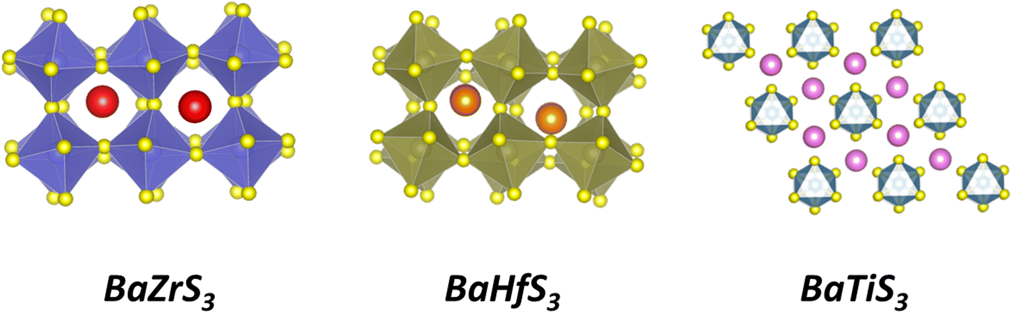 | ||
| Fig. 1 Crystal structures of BaZrS3, BaHfS3, and BaTiS3. BaZrS3 and BaHfS3 exhibit distorted perovskite structures, while BaTiS3 adopts a hexagonal crystal structure. | ||
Other than BaZrS3, Sr-based perovskites have also garnered notable interest from the research community due to their similarly exciting properties, with SrHfS3 exhibiting strong green emission.41–45 While the term “chalcogenide perovskites” is frequently used, this family of compounds predominantly consists of sulfide materials, with LaScSe3 being the only selenide perovskite reportedly grown under thermal equilibrium growth conditions.46 Additionally, some tellurium-based compounds have been predicted, such as ACeTe3 (A = Ca, Sr, and Ba), which take on a distorted perovskite phase, though they have not yet been experimentally synthesized.47 Beyond ABX3 phases, the Ba–Zr–S system also supports the formation of layered 2D Ruddlesden–Popper phases. These phases have been shown to have lower bandgaps compared to BaZrS3, with strong photoluminescence and high carrier lifetimes, making them promising for optoelectronic applications.27,28,48–51 However, these compounds have primarily been reported as phase-pure only at high temperatures, and their challenging synthesis remains a bottleneck.48 Moreover, some first-principle studies have reported exciting combinations of double chalcogenide perovskites, though their syntheses have not yet been achieved.52–54
The lower electronegativity of chalcogenides compared to oxides or halides leads to reduced electronegativity differences between the cations and anions, thereby decreasing the ionic nature of the bonds and increasing covalency. This increased covalency contributes to achieving bandgaps in the visible range for chalcogenide perovskites. Jess et al. and Turnely et al. argued that due to the increased covalency in chalcogenide perovskites, using Shannon ionic radii derived from oxide materials in geometric factors is not ideal for predicting the structure of chalcogenide perovskites. They have proposed modifications to the existing rules to determine the correct phase, such as including the electronegativity differences between the cation and anion in predictions and utilizing ionic radii derived from a sulfide dataset instead. Their studies have also led to the prediction of a host of new possible chalcogenide perovskites, which should be further explored.55,56
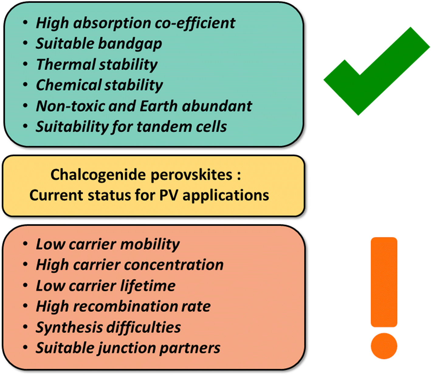
All synthesized chalcogenide perovskites exhibit promising properties, and their varying bandgaps make them suitable for various applications (see Fig. 2). Notably, these materials feature tunable bandgaps, which can be adjusted by changing the elements in the structure or by alloying different elements, resulting in a wide range of bandgap values.23,57–61 Despite crystallizing in the perovskite structure, they offer enhanced stability against air, moisture, and heat, combining the attractive features of the perovskite crystal structure with the robustness of chalcogenide semiconductors.48,62–65 Composed of earth-abundant elements primarily sourced from the top 20 elements in the Earth's crust, they align with sustainability goals (see Fig. 3 for the relative abundance of elements).23,66 DFT-predicted high absorption coefficients on the order of 105 cm−1 have been experimentally confirmed.67,68 Additionally, properties such as high dielectric constant, low thermal conductivity, and high Seebeck coefficient suggest potential applications beyond photovoltaics.66,69Fig. 4 shows the high dielectric constant observed for cold-sintered BaZrS3 powder and BaZrS3 single crystals, among the highest reported for chalcogenide semiconductors. While other expected properties, such as strong photoluminescence, defect tolerance, and high carrier mobility, require further experimental validation, chalcogenide perovskites remain in the early stages of research and development. The only reported device utilizing chalcogenide perovskites in a typical thin film architecture has been demonstrated for LaYS3, indicating significant opportunities for other chalcogenide perovskite materials.70 Additionally, other notable candidate of this family Ca3Sn2S7 has been predicted to possess graphene-like linear electronic dispersion, an ultrasmall effective mass, and high carrier mobility.71
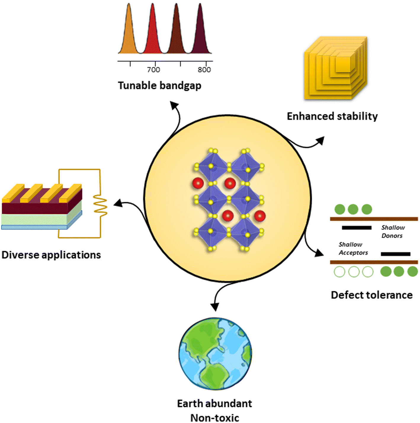 | ||
| Fig. 2 Schematic highlighting the notable properties of chalcogenide perovskites. | ||
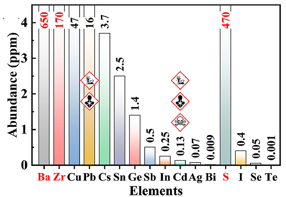 | ||
| Fig. 3 Schematic illustrating the relative abundance of Ba, Zr, and S in comparison to other key elements utilized in thin-film photovoltaic applications. Reproduced with permission.66 Copyright 2024, Elsevier. | ||
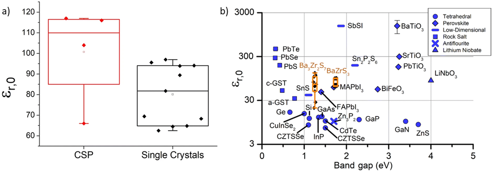 | ||
| Fig. 4 Dielectric constant of BaZrS3 and other inorganic materials. (a) Comparison of the dielectric constant for densified BaZrS3 obtained through cold-sintering and single crystal BaZrS3. (b) Plot illustrating the relationship between the dielectric constant and bandgap for various inorganic materials. (a) and (b) Reproduced with permission.69 Copyright 2021, Springer Nature. | ||
The synthesis of these materials has been reported in the literature with varying levels of difficulty, with BaZrS3 and BaHfS3 being synthesized at the lowest temperatures.62,72–74 Among these, BaZrS3, with its ideal bandgap of 1.7–1.9 eV for photovoltaic applications, has exhibited defect tolerance and a high dielectric constant. However, a deeper understanding of the key factors for achieving phase-pure synthesis is required. Despite significant progress in synthesizing BaZrS3 at high temperatures, efforts to replicate this success at lower temperatures (<600 °C) more suitable for practical applications have been challenging. Although many reports have successfully produced contiguous BaZrS3 films at high temperatures, none have achieved this at lower temperatures, highlighting a significant hurdle.48,62Fig. 5 summarizes the strengths of chalcogenide perovskites (especially BaZrS3) and the areas where further work is needed.
 | ||
| Fig. 5 Schematic depicting the current status of chalcogenide perovskites, with a particular focus on BaZrS3, in photovoltaic applications. | ||
Due to the high potential of BaZrS3 in photovoltaic applications and significant interest from the research community in advancing this material, this report aims to review successful synthesis methods for BaMS3 (M = Ti, Zr, Hf) compounds and their intriguing properties and applications. Additionally, it provides insights to bridge the gaps in synthesis methods, paving the way for the fabrication of contiguous BaMS3 films at low temperatures within practical time frames.
2. Synthesis of BaMS3 compounds
Chalcogenide perovskites, often seen as potential high-performing alternatives to halide perovskites, have struggled to match the rapid advancement of their halide counterparts, primarily due to the harsh growth conditions required for their synthesis. BaZrS3 is one of the most extensively studied chalcogenide perovskites, owing to its optimal bandgap and relative ease of synthesis compared to other chalcogenide perovskites. However, the synthesis temperatures for BaZrS3 have typically been much higher than those required for other chalcogenide semiconductors such as Cu(In,Ga)Se2, Cu2ZnSnSe4, and AgInSe2.75–79 Nonetheless, recent years have witnessed the development of numerous methods for the synthesis of BaZrS3 and other chalcogenide perovskites. These methods range from flux-driven solid-state synthesis and epitaxial-based film growth techniques to solution-processing approaches, among others (see schematic in Fig. 6 for the four broad class of synthesis methods).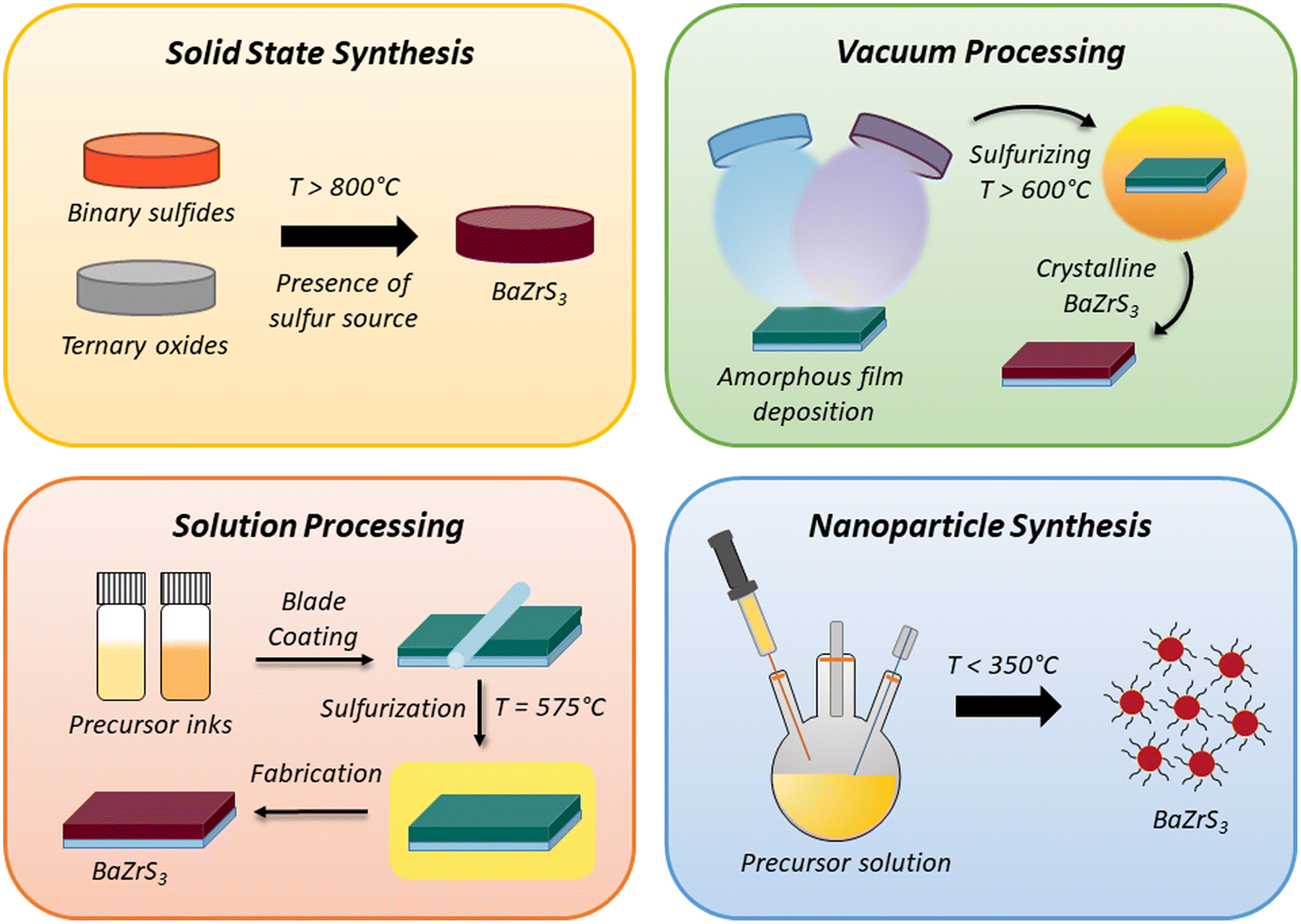 | ||
| Fig. 6 Schematic illustrating the various synthesis methods used for the preparation of BaZrS3 and related compounds. | ||
2.1. High-temperature synthesis
Despite these challenges, the preferred method for the solid-state synthesis of BaMS3 compounds has been the CS2 sulfurization of oxide powders. This process involves continuously flowing CS2 through oxide powders maintained at temperatures exceeding 1000 °C for several hours to days.40,48,83–86 In this method, oxide materials were reduced to their sulfide forms. According to thermodynamic calculations by Agarwal et al., CS2 sulfurization of oxides is thermodynamically feasible at lower temperatures (<600 °C) but may not be kinetically feasible at these temperatures.73 Nishigaki et al. demonstrated a synthesis approach that involved mixing binary sulfide powders, pelletizing them, and subsequently annealing at temperatures exceeding 1000 °C for several days.67 Additionally, single crystals of BaZrS3 have been produced using the BaCl2 flux and I2 vapor transport methods.27,28,64 In both instances, barium sulfide, zirconium powder, and sufur pieces were combined with flux to accelerate mass transfer, resulting in several microns in size crystals. While these methods successfully achieved the desired crystal sizes, they pose a risk of leaving behind chlorine or iodine impurities in the growing crystals due to the high affinity of alkaline earth metals for halides. This could impact the material's intrinsic properties, which are not yet fully understood.
In an attempt to create dense pellets of BaZrS3, Filippone et al. achieved high densification of BaZrS3 powders at 450 °C and 425 MPa by adding approximately two wt% iodine.87 Their method, conducted under ambient conditions, did not lead to significant oxidation. Moreover, the boron-chalcogen method has previously been shown to convert various metal oxides into metal sulfides at moderate temperatures. Bystrický et al. extended this method to chalcogenide perovskites, using metal oxides and carbonates as precursors to form ternary compounds.88 Notably, they obtained nearly phase-pure BaZrS3 from oxide precursors at 600 °C within a few hours of heat treatment using their flowing tubular furnace (see Fig. 7a). However, this method can introduce residual boron impurities into the target material. Although boron oxide is water soluble and can be removed with a light water wash, some water-insoluble boron oxysulfide impurities may remain.
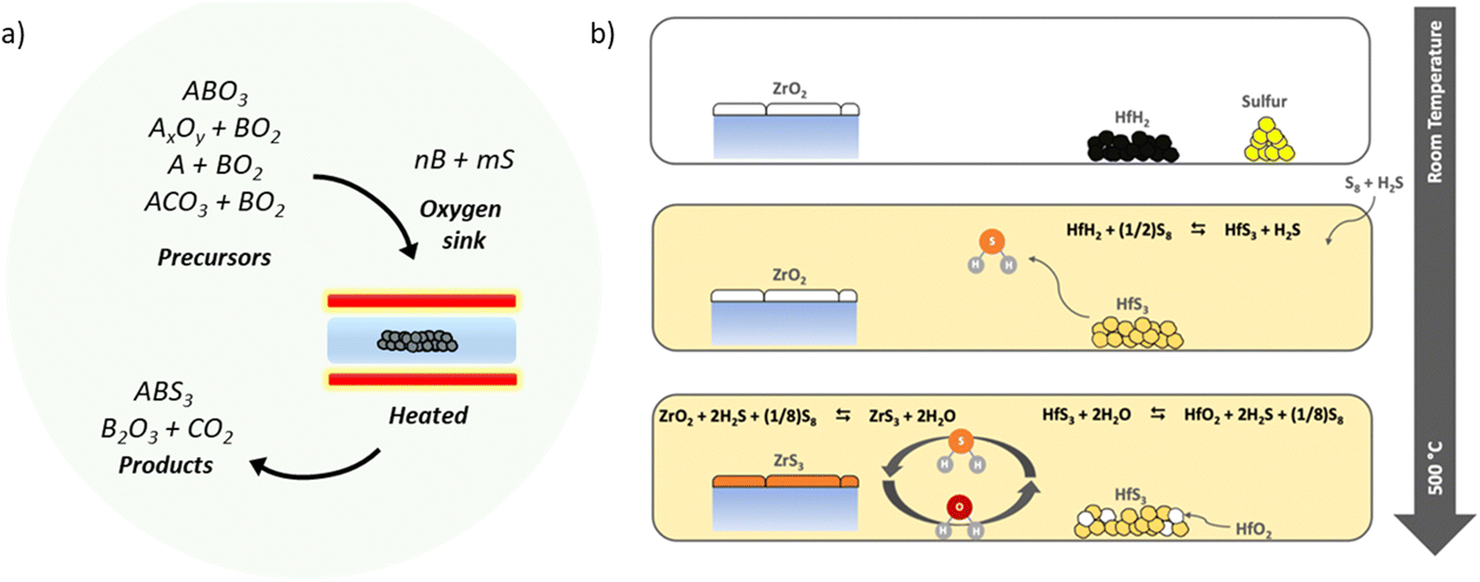 | ||
| Fig. 7 (a) Schematic illustrating the conversion of binary and ternary oxide powders into ternary chalcogenides using boron and sulfur. (a) Adapted with permission.88 (b) Schematic depicting the conversion of ZrO2 into ZrS3 using HfH2 and sulfur. (b) Reproduced with permission.73 Copyright 2023, Royal Society of Chemistry. | ||
In another significant contribution, Agarwal et al. used HfH2 and sulfur in ampule sulfurization to create an H2S–HfS3 oxygen shuttle-sink system that converts oxide materials into sulfides at temperatures up to 600 °C (schematic shown in Fig. 7b).73 This approach is notable because Hf does not interact with the BaZrS3 film, thus avoiding potential impurity contamination.
In recent notable advancements, the Jaramillo group at MIT successfully grew BaZrS3 films on LaAlO3 substrates using molecular beam epitaxy with an atomically sharp interface. Fig. 8a shows the lattice constants of commonly available commercial substrates and chalcogenide perovskites. They deposited thin films using elemental Ba and Zr alongside H2S gas with the substrate temperature maintained at 900 °C.89 The films grew through two different mechanisms: buffered epitaxy, which creates a specific interface layer to alleviate strain, and direct epitaxy, in which the layers rotate to align despite significant differences in lattice size between the oxide and sulfide perovskites (shown in Fig. 8b). However, the epitaxially grown films exhibited planar defects, including antiphase boundaries, as demonstrated in Fig. 8c. Nonetheless, this method holds the potential for tuning the structure of sulfide perovskites and investigating the resulting properties. The group also expanded this technique to become the first, and currently the only, method to synthesize BaZr(S,Se)3 films.90
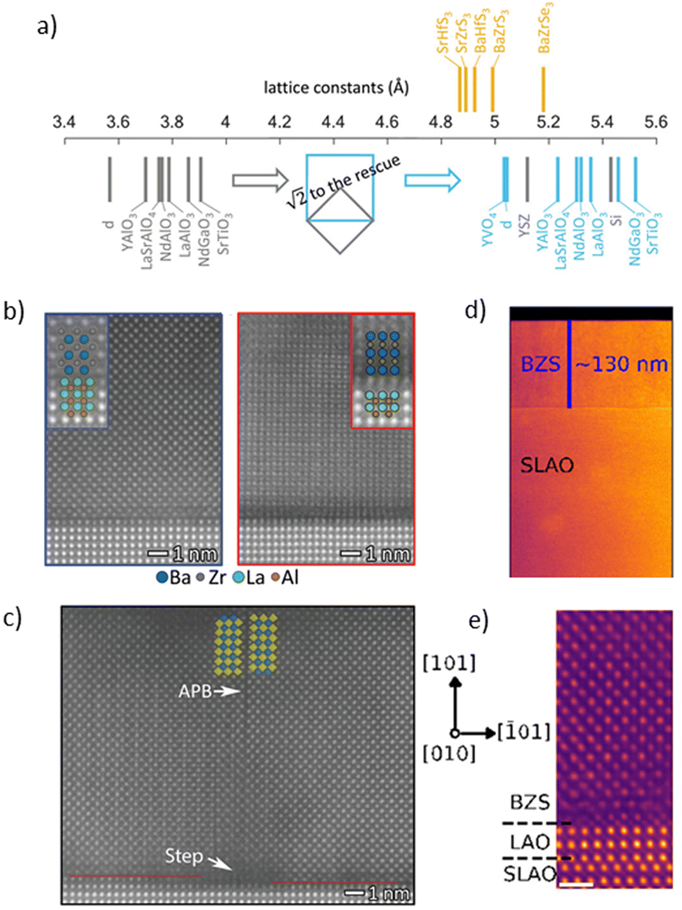 | ||
| Fig. 8 Epitaxially grown BaZrS3. (a) Comparison of pseudocubic lattice constants for chalcogenide perovskites and commercially available crystal substrates: d, diamond; YSZ, yttria-stabilized zirconia. Orange represents selected chalcogenide perovskites, gray denotes pseudocubic lattice constants of commercially available substrates, and blue indicates pseudocubic lattice constants scaled by a factor of sqrt 2. (b) HAADF STEM images of a BaZrS3 film grown on an LaAlO3 substrate, showing two distinct epitaxial growth modes: (b1) the predominant mode with pseudocubic edges aligned (growth mode M1), and (c1) the rotated cube-on-cube mode with direct bonding (growth mode M2). Insets display magnified images with overlaid atomic species. (c) STEM HAADF images revealing planar defects, including antiphase boundaries located at substrate step edges. Yellow and blue squares denote dimmer (Zr/S) and brighter (Ba) atom columns, respectively, adjacent to the antiphase boundary. Atom columns associated with growth mode M2, which may nucleate at substrate steps, are also faintly visible in the left-center region of the image. (a)–(c) Reproduced with permission.89 Copyright 2021, Wiley. (d) HAADF image of BaZrS3 (BZS) film grown on an SLAO substrate, along with an image showing the polycrystalline nature of the BZS film. (e) Atomic-resolution HAADF images of the BZS/SLAO interface, indicating the orientation of the BZS film in this region. (d) and (e) Reproduced with permission.72 Copyright 2021, American Chemical Society. | ||
Previously, Ravichandran group developed epitaxial BaZrS3 thin films using pulsed laser deposition (PLD) on LaAlO3/SrLaAlO4 substrates (see Fig. 8d).72 They employed BaZrS3 as the target material and deposited films with a background of H2S–Ar, depositing films in a single step at relatively low temperatures of 700–850 °C. The significant variations in vapor pressure between the cations and sulfur source presented challenges, which their approach sought to address. While the films displayed epitaxial qualities near the film–substrate interface (as can be seen in Fig. 8e), they exhibited extended defects such as grain boundaries and Ruddlesden–Popper faults further from the interface. Surendran et al. also attempted to grow epitaxial films of quasi-1D BaTiS3 using the same method, finding that the films exhibited weak epitaxial growth near the interface but were highly textured in the out-of-plane direction.91
The CS2 sulfurization of oxide powders has proven successful in converting oxide powders into sulfides. However, the process is energy-intensive and typically requires high-temperature treatments. Koratkar group adapted CS2 sulfurization to films by depositing oxide films using solution deposition and heating them with a flowing mixture of CS2 and nitrogen at temperatures exceeding 1050 °C (depicted in Fig. 9a).62,92 This approach resulted in relatively uniform polycrystalline BaZrS3 thin films on quartz substrates. While notable, this method may lead to some oxide impurities in the film and thus requires careful evaluation.
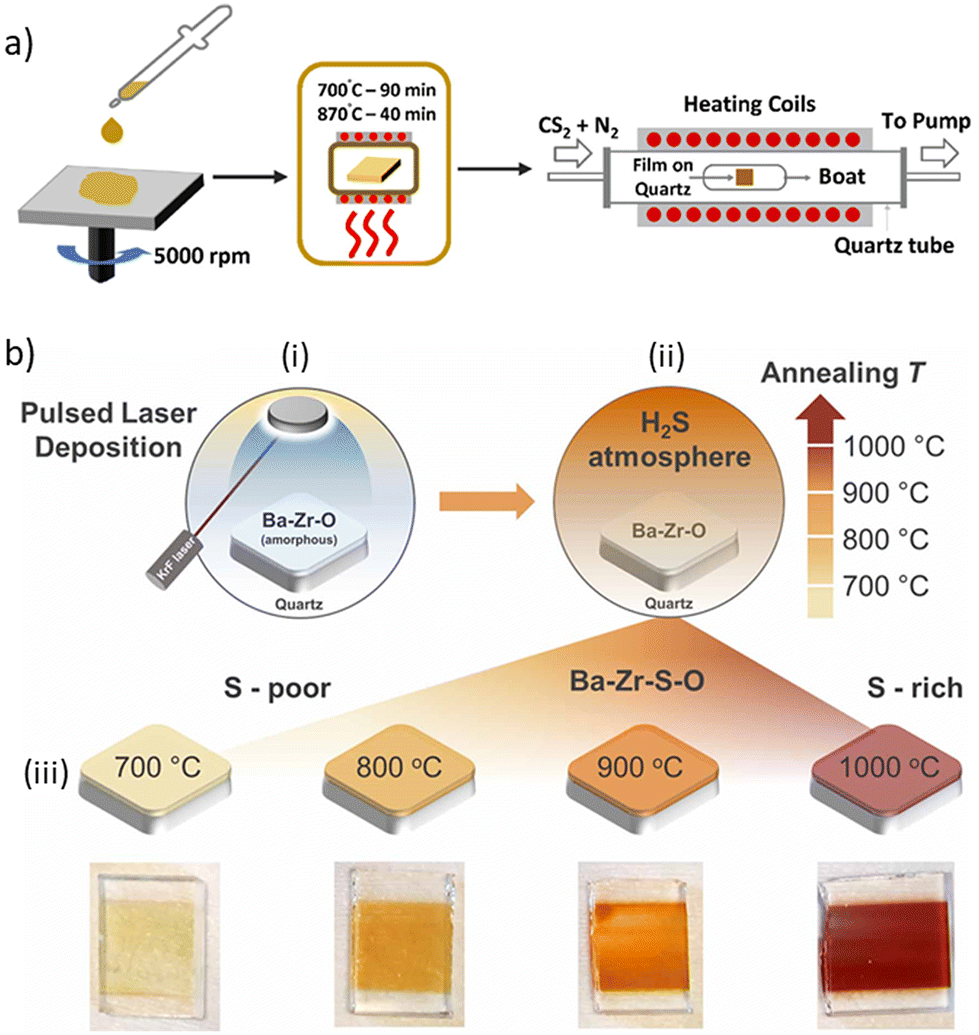 | ||
| Fig. 9 Conversion of Ba–Zr–O into BaZrS3 at temperatures exceeding 900 °C. (a) Schematic illustrating the synthesis of BaZrS3 film from an oxide precursor film, which is sulfurized in a CS2 environment. (a) Reproduced with permission.96 Copyright 2021, American Chemical Society. (b) Schematic depicting the synthesis of BaZrS3 film from a pulsed laser deposited amorphous Ba–Zr–O film, followed by sulfurization with H2S. (b) Reproduced with permission.95 Copyright 2023, IOP Science. | ||
Similarly, Zeng group deposited BaZrO3 film and amorphous Ba–Zr–S film using pulsed laser deposition (PLD) and converted them to BaZrS3 using CS2 sulfurization.57,86,93 In another study, Dhole et al. used an aqueous solution route via polymer-assisted deposition (PAD) and sulfurized polymer-chelated cation precursor films with a flowing mixture of CS2 and argon at 900 °C.94 Although their approach is significant, the resulting films exhibited a polycrystalline texture with nanometer-sized grains.
While CS2 sulfurization is a more common method for converting oxide films into ternary sulfides, H2S sulfurization has also been explored in some studies. Márquez et al. sulfurized their amorphous Ba–Zr–O films at temperatures ranging from 700–1000 °C under a continuous flow of 5% H2S, finding increased crystallinity and sulfur content at higher temperatures.68 However, the sulfurized films contained notable oxide impurities along with ternary BaZrS3, with the sulfur content reaching a maximum of 0.85 S at%/(S at% + O at%). They also reported that no solid solution of BaZrO3 and BaZrS3 was observed, and separate diffraction peaks for BaZrO3 and BaZrS3 were present.
Ramanandan et al. investigated the sulfurization mechanism of amorphous Ba–Zr–O films using H2S treatment.95 They found that the initial amorphous Ba–Zr–O film converted into crystalline BaZrO3 and amorphous Ba–Zr–S at 700 °C. The crystalline BaZrO3 became amorphous at higher temperatures, forming an amorphous Ba–Zr–O–S phase from which crystalline BaZrS3 nucleated alongside ZrO2 at temperature increased above 900 °C (see Fig. 9b). Their study suggests that the diffusion of sulfur-containing species is the rate-limiting step, necessitating high-temperature synthesis. It also highlights that low partial pressures of H2S may not completely sulfurize the oxide film in a reasonable time due to slow kinetics. A mixture of H2 and H2S could be tested, as H2 could aid in removing oxides while H2S sulfurizes the film. However, concentrations of H2S exceeding 4.3% in air become flammable and pose a safety hazard, so proper protocols must be followed.
In a notable achievement, Comparotto et al. synthesized BaZrS3 films by annealing amorphous Ba–Zr–S films, initially deposited via physical vapor deposition (PVD) at varying temperatures starting at 600 °C. They found that the phase purity of BaZrS3 films improved as annealing temperatures increased to 900 °C, after which secondary oxide phases were observed at 1000 °C.97
All the above methods relied on a mixed precursor film to synthesize BaZrS3. In an alternative approach, Freund et al. proposed a bilayer strategy in which they deposited a BaS layer onto zirconium foil and then sulfurized it in a flowing sulfur vapor environment at temperatures below 500 °C.98 However, this process resulted in the formation of BaS3 film without the nucleation of ternary BaZrS3, potentially due to surface oxidation of the Zr foil or diffusion limitations at the operating temperatures, which prevented the reaction of BaS3 with Zr to form a ternary phase. Similarly, Jamshaid et al. applied a 300–600 nm layer of BaS onto a zirconium layer on a SiC substrate and sulfurized it under flowing sulfur at 1000 °C, resulting in BaZrS3 nucleation.99
Overall, these high-temperature methods provide valuable insights into the reactivity of various sulfur sources in converting oxides into sulfides. They also emphasize the challenges of sulfurizing highly stable oxide phases and underscore the need for using more reactive precursors to achieve faster kinetics and complete conversion.
2.2. Low-temperature synthesis
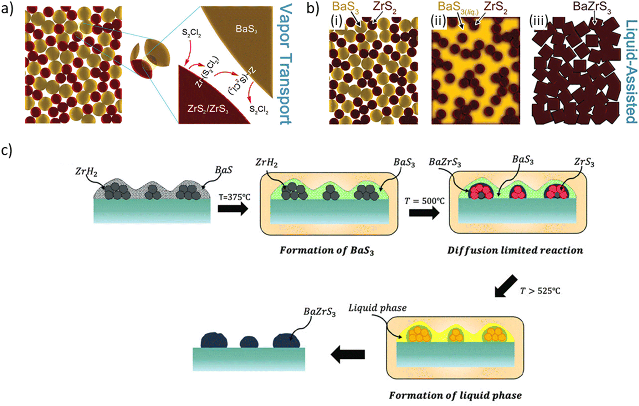
Wang et al. achieved a notable milestone by synthesizing BaZrS3 at 500 °C using a BaCl2 flux in the presence of excess sulfur, representing the lowest reported temperature for producing phase-pure BaZrS3 in bulk form.102 Yang et al. later elucidated the mechanism of this reaction, explaining that sulfur interacts with chlorine from BaCl2 to form S2Cl2 vapor, which acts as a transport agent and reduces the synthesis temperature. Confirming their hypothesis, they sealed binary sulfide precursors in an ampule with S2Cl2 liquid and reacted them at 500 °C for 3 hours, successfully producing phase-pure BaZrS3 (see Fig. 10a).100 Similarly, Ravi et al. synthesized BaZrS3 nanopowder using BaS, Zr, and stoichiometric sulfur at 600 °C with the assistance of an I2 transport agent.65 Despite the benefits of lowering the synthesis temperature, both S2Cl2 and I2 may introduce chlorine and iodine impurities, respectively, which could adversely affect the intrinsic properties of emerging semiconductors that are not yet fully understood. We performed thermodynamic calculations to validate this hypothesis, confirming that barium possesses one of the highest affinities for halide atoms among all elements in the periodic table.103
 | ||
| Fig. 10 Schematic illustrating the working principles of: (a) S2Cl2 vapor transport agent, (b) BaS3 liquid flux, and (c) BaSx (x > 3) liquid flux. (a) Reproduced with permission.100 Copyright 2023, American Chemical Society. (b) Reproduced with permission.101 Copyright 2023, Wiley. | ||
An ideal flux would consist of the same elements that form the desired compound, minimizing the potential for unwanted impurities. In this context, Vincent et al. identified a liquid flux of BaSx (x > 3) that forms at temperatures above 525 °C in a saturated sulfur environment, suitable for synthesizing BaMS3 compounds.101 They demonstrated the efficacy of this method on thin-film samples prepared using a hybrid precursor solution-processing route previously established by the Agarwal group,74 verifying the formation of a liquid BaSx flux that reacted with in situ generated ZrS3 from ZrH2, enabling the nucleation of BaZrS3 within 5 minutes at 575 °C (see Fig. 10c). They further applied this approach to the bulk solid-state synthesis of BaZrS3 using BaS, ZrS2, and excess sulfur, achieving synthesis within 15 minutes at 575 °C. This starkly contrasts with previous solid-state reactions at temperatures above 900 °C over several hours to days.
Building on these advances, Yang et al. suggested that BaS3 could act as a liquid flux in the synthesis of BaMS3 compounds, as BaS3 melts between 540 °C and 560 °C. However, according to the Ba–S phase diagram, BaS3 dissociates into BaS2 and a sulfur-rich BaSx at 554 °C.104 Thus, it is likely that BaSx provides the actual liquid flux. Interestingly, they loaded large amounts of stoichiometric BaS3 and ZrS2 into an ampoule and heated the mixture to 540 °C, forming BaZrS3 within 5 minutes (as shown in Fig. 10b). During this process, BaS3 likely dissociated into BaS2 and then into BaS, creating a saturated sulfur environment at 540 °C while simultaneously providing a BaSx liquid flux, which accelerated the growth of BaZrS3.100
In a recent noteworthy report, our group demonstrated that selenium can also provide a liquid flux and lower the synthesis temperatures of BaMS3 compounds.105 Using an excess of selenium liquid flux, we successfully synthesized BaMS3 compounds at 575 °C starting from binary metal sulfide precursors. Although small amounts of BaSe3 impurities were observed, they were found to be water-soluble. Consequently, a slight water wash of the synthesized powder resulted in seemingly phase-pure BaMS3 compounds.
Overall, these low-temperature methods have significantly advanced the research on BaMS3 compounds and paved the way for synthesizing them into thin films at lower temperatures.
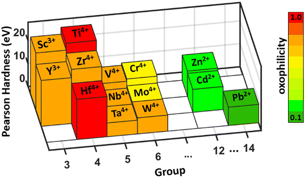
Kepp proposed an oxophilicity scale, which is a relative measure of an element's affinity for oxygen compared to the most oxophilic element in the periodic table.82 Zilevu et al. noted that group IV elements rank among the most oxophilic elements in the periodic table with the highest oxophilicity, readily oxidizing upon exposure to air and moisture (shown in Fig. 11).81 Pearson hardness is another parameter that accounts for the high oxophilicity of early transition metals. It is derived from the hard and soft acids and bases (HSAB) theory, which states that hard acids, such as cations with small size and high charge, preferentially bond with hard bases, which are typically anions with small size, high charge, and high electronegativity. As a result, hard acids (early transition metals) exhibit a strong affinity for hard bases (such as oxygen), explaining the high oxophilicity of early transition elements (see Fig. 11). This oxophilicity poses a significant challenge when dealing with molecular precursors, as their susceptibility to interaction with oxygen and moisture increases, leading to the formation of undesired oxides. Addressing this issue, Agarwal et al. introduced the aforementioned HfS3–H2S shuttle system to eliminate secondary oxides from molecular precursor films during sulfurization.73 In their approach, they sulfurized the Ba–Zr–O film with excess sulfur in the presence of HfH2. HfH2 reacted with sulfur vapor, generating HfS3 and in situ H2S gas. The produced H2S gas then reacted with Ba–O and Zr–O species in the film, forming Ba–S and Zr–S species while releasing H2O. The generated H2O was transported to HfS3, leading to the formation of HfO2 and the regeneration of H2S. Due to the discrepancy in oxophilicity between Hf and Zr, oxygen was effectively transferred from the Ba–Zr–O film to HfS3. Concurrently, the surplus sulfur vapor in the film facilitated the production of BaSx liquid flux, reducing the diffusion barrier between Ba and Zr species and promoting rapid nucleation and growth of BaZrS3 grains. This HfS3–H2S shuttle has been employed in the low-temperature, oxide-free, solution-processed synthesis of BaZrS3 (Fig. 7b).
 | ||
| Fig. 11 Plot showing the Pearson hardness and oxophilicity of common transition elements. Reproduced with permission.81 Copyright 2023, Royal Society of Chemistry. | ||
Metal chlorides are commonly used as precursors in the solution-processed synthesis of other chalcogenide semiconductors.78,112 However, we previously observed an abundance of residual crystalline alkaline earth metal chloride impurities in the film following the dissolution of alkaline earth metal chlorides in N,N-dimethyl formamide – thiourea chemistry, annealing on a hot plate, and sulfurization in a sulfur environment.113 This phenomenon likely stemmed from the greater stability of metal–chlorine bonds compared to metal–sulfur bonds for alkaline earth metals at operational temperatures. This is particularly interesting, as Yang et al.100 used S2Cl2 as a vapor transport agent to synthesize BaZrS3. We believe the key is to maintain a much lower molar fraction of chlorine-containing species to prevent the significant formation of Ba–Cl compounds, which could interfere with the formation of BaZrS3. However, existing literature on other chalcogenide semiconductors advocates using impurity-free metal precursors in absorber material synthesis, as metal salt precursors may leave behind anionic impurities in the film, potentially altering its intrinsic properties uncontrollably.76,114,115 Consequently, Pradhan et al. explored the dissolution of ZrS2 and HfS2 in various amine–thiol combinations, such as 1,2-ethanedithiol-1,2-ethylenediamine and 1,2-ethanedithiol–butylamine, among others, with no success.113 Additionally, attempts using hydrazine chemistry to dissolve sulfides of various early transition metals including ZrS2 and HfS2 proved futile. Similar efforts with pure zirconium and hafnium nanoparticles in amine–thiol solutions yielded no positive outcomes.113 Moreover, there is a dearth of reports on the successful dissolution of pure alkaline earth metals and their binary sulfides, raising uncertainty about their compatibility with common sulfide chemistries or the extent of rigorous testing. Despite these challenges, one study noted the co-dissolution of BaS alongside Cu2S and SnO in an ethanedithiol–ethylenediamine mixture at 60 °C for 11 days.116 However, whether BaS alone would dissolve in the amine–thiol mixture remains unclear, as subsequent research has not explored BaS dissolution. In a recent report, our group successfully dissolved BaS and SrS using a different solution chemistry, which will be discussed later.105 In summary, common precursors utilized in the solution-based synthesis of chalcogenide semiconductors for the late transition and p metals face obstacles in synthesizing chalcogenide perovskites. It is worth noting that during the peer-review stage of this study, another work of ours was published, where we demonstrated a method to synthesize BaMS3 compounds using single-phase metal chloride precursor solutions.103 This approach leveraged the higher affinity of potassium for chlorine compared to barium, enabling the transfer of residual chlorine in the film to a potassium sink during the annealing process via an H2S–HCl shuttle. This method effectively resulted in chloride impurity-free BaZrS3. Readers are encouraged to refer to the publication for further details.
The reactivity of starting precursors plays a crucial role in determining the success and efficiency of material synthesis processes. Highly reactive precursors tend to undergo chemical reactions more readily, leading to faster kinetics and potentially more complete conversion to the desired product. This can result in shorter synthesis times and higher yields. Conversely, less reactive precursors may require longer reaction times or higher temperatures to achieve the desired transformation, and they may also yield lower product yields. Additionally, the reactivity of precursors can influence the formation of by-products or impurities during the synthesis process. Therefore, selecting precursors with appropriate reactivity levels is essential for controlling the synthesis conditions and obtaining the desired material properties.
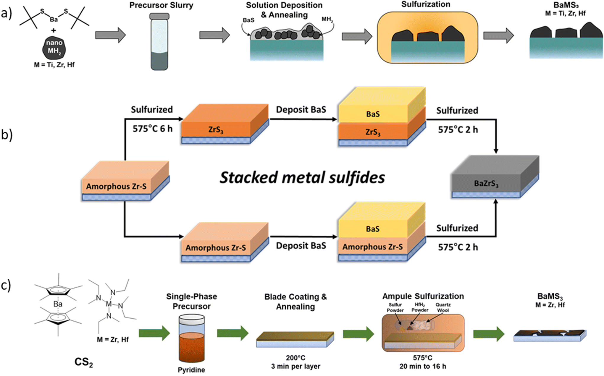
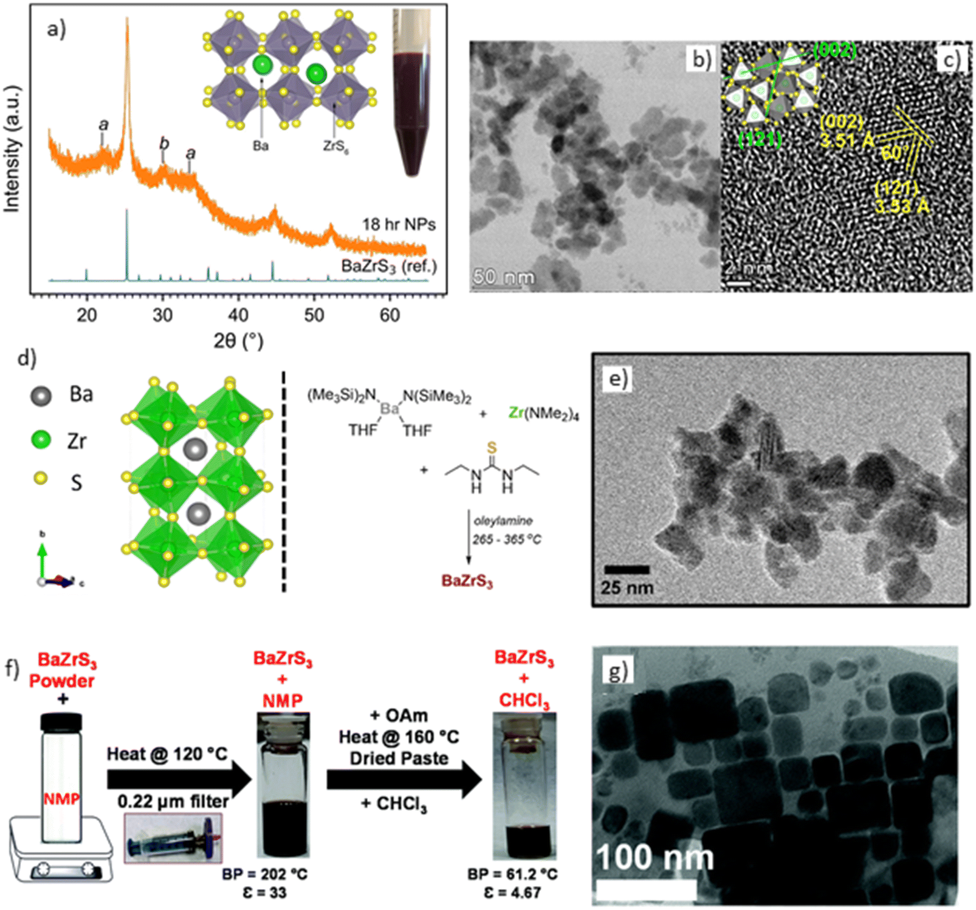
Focusing on precursor reactivity, our group utilized organobarium bis(pentamethylcyclopentadienyl)barium (Cp*2Ba) as the barium precursor, reacting it with branched primary thiol 2-methyl-2-propanethiol to form Ba(SC(CH3)3)2, which were found to be readily soluble in primary amines like propylamine and butylamine.74 However, it remains unclear whether other primary and secondary thiols would react similarly with Cp*2Ba to form soluble thiolate species. It is plausible that the branched thiol aided solubility in less polar amine solvents. Further experiments are needed to confirm this hypothesis. Turnley et al. also employed ZrH2 as the zirconium precursor, suspending it in a barium solution in butylamine and sonicating it to create a uniform suspension for depositing Ba–Zr precursor films.74 The choice of zirconium precursor is somewhat peculiar, given the availability of more common metal–organic precursors for zirconium used in chemical vapor deposition processes. The possible reason for not using a metal–organic precursor may be attributed to zirconium's oxophilicity, as metal–organic species are highly reactive and prone to oxide formation. The Zr–H bonds are relatively stable and do not oxidize immediately upon air exposure. Using the hybrid precursor method, the solution was drop-cast onto a glass substrate and then sulfurized at 575 °C for 2 hours in a borosilicate ampule (schematic shown in Fig. 12a). Subsequently, we followed a similar method and synthesized BaZrS3 in as little as 5 minutes at 575 °C with excess sulfur. It was proposed that the drop-cast film formed a mixture of BaS and ZrH2, which upon sulfurization with excess sulfur, transformed into BaSx liquid and ZrS3, facilitating rapid BaZrS3 synthesis. While both studies demonstrated BaZrS3 synthesis at moderate temperatures, the hybrid precursor route yielded non-contiguous thin films.101 A potential approach to contiguous films could involve functionalizing the surface of ZrH2 nanoparticles to achieve colloidal stability in the same bulk solvent as the soluble barium precursor, albeit no reports on this have surfaced yet, making it an area worthy of exploration.
 | ||
| Fig. 12 Schematic representation of the synthesis of solution-processed BaMS3 (M = Ti, Zr, Hf) films. (a) Synthesized from a precursor slurry containing soluble barium thiolate and suspended transition metal hydride precursors. Reproduced with permission.74 Copyright 2022, American Chemical Society. (b) Synthesized from a stacked precursor film of BaS and transition metal sulfides. Reproduced with permission.105 Copyright 2024, Royal Society of Chemistry. (c) Synthesized from soluble barium dithiocarboxylate and transition metal dithiocarbamate precursors. In all cases, the precursor films underwent a sulfurization step in a sulfur-rich environment to induce the crystallization of the ternary chalcogenides. Reproduced with permission.117 Copyright 2023, Wiley. | ||
In other noteworthy synthesis methods from our group, we reacted propylamine with CS2 to form propyldithiocarbamic acid and used pyridine as a buffer solvent to dissolve the acid. This highly reactive dithiocarbamic acid species formed soluble complexes with BaS and SrS at room temperature, resulting in fully dissolved molecular precursor inks.105 While ZrS3 could not be dissolved, it was suspended in pyridine and sonicated to break down the smaller flakes, creating a stable suspension. The BaS and ZrS3 solutions in pyridine were mixed to create a solution containing both barium and zirconium sulfide precursors. Upon coating on a glass substrate and sulfurization, this solution yielded phase-pure BaZrS3, marking the first report of synthesizing BaZrS3 using metal sulfide precursors at lower temperatures. In another method, we created a bilayer stack of BaS and ZrS3 from the molecular precursor inks on a substrate. The ZrS3 was synthesized from the molecular precursor solutions utilizing zirconium halide precursors, and the stacked film was sulfurized in a sulfur environment, accessing BaSx liquid flux and forming BaZrS3 (see Fig. 12b). This method represents the first synthesis of BaZrS3 using Zr halide precursors.105
In a significant breakthrough, our group employed tetrakis amide precursors of zirconium as the metal source for synthesizing BaZrS3. These precursors are commercially available and widely used in chemical vapor deposition processes.117 Previously, Thompson demonstrated the utility of these precursors in his thesis, employing various sulfur sources such as carbon disulfide and ethyl isothiocyanate to form single-source metal–sulfur bonded precursors, ultimately synthesizing ZrS2via chemical vapor deposition.118 Pradhan et al. utilized Zr[N(MeEt)4] as the zirconium precursor and inserted carbon disulfide in the metal amide bond to form zirconium dithiocarbamate species. Additionally, carbon disulfide was inserted into Cp*2Ba to generate a barium dithiocarboxylate precursor. While barium dithiocarboxylate proved soluble in pyridine, independent dissolution of tetrakisamido ethylmethylzirconium dithiocarbamate in pyridine was not feasible. However, co-dissolving barium and zirconium precursors in pyridine along with CS2 resulted in the first reported fully dissolved molecular precursor ink at room temperature for the synthesis of BaZrS3. However, similar success was not achieved with the dimethyl amide precursor of zirconium. The fully dissolved ink was then blade-coated and annealed on a hot plate, resulting in an amorphous matrix of Ba–Zr–S. Subsequent sulfurization with excess sulfur in the presence of HfH2 at 575 °C for as little as 20 minutes yielded BaZrS3, marking a significant improvement over previous high-temperature synthesis methods (>900 °C) (schematic shown in Fig. 12c). Pradhan et al. also observed increased crystallinity of BaZrS3 grains, as indicated by the reduced full width at half maximum (FWHM) of the 25.2 peak, with longer sulfurization times.117 Although not explicitly stated, the localized formation of BaSx liquid flux likely facilitated BaZrS3 nucleation and grain growth. Despite these advancements, further refinement is needed to address irregularly oriented agglomerates of cubic-shaped crystals and excessive carbon content known to influence grain size and composition during growth. Rigorous optimization of annealing parameters, sulfur amount, and substrate choice may be necessary to produce device-grade continuous films.
These reports have played a pivotal role in achieving thin films of BaZrS3via solution processing. However, several challenges persist. All the aforementioned methods relied on BaSx liquid flux for crystal growth, resulting in rapid, uncontrolled growth and the formation of large micron-sized grains (see Fig. 13a and b). Thus, there is a pressing need to develop strategies to mitigate uncontrolled growth. During the revision stage of this work, another manuscript from our group was published, introducing several novel methods for synthesizing BaZrS3 thin films, some of which successfully produced contiguous films.119 Notably, one method utilized metal thiolate precursors to synthesize BaZrS3 without the need for HfH2, and also prevented the overgrowth of BaZrS3 grains. Further details can be found in the published article. Nonetheless, several challenges remain to be addressed. Due to BaZrS3's high absorption coefficient, a thin film as thin as 200 nm should suffice to fully absorb incoming light. However, the solution methods discussed have so far yielded films several microns thick, that could potentially impede the collection of light-generated charge carriers and impact performance of fabricated devices. Moreover, these films were grown on non-conductive substrates, necessitating further efforts to replicate them on conductive substrates. This endeavor presents challenges, as the metal back contacts used in many device architectures may sulfurize to their sulfides when exposed to prolonged sulfur environments. Consequently, additional research is required to identify a suitable, cost-effective, conductive back contact capable of withstanding prolonged exposure to sulfur environments.
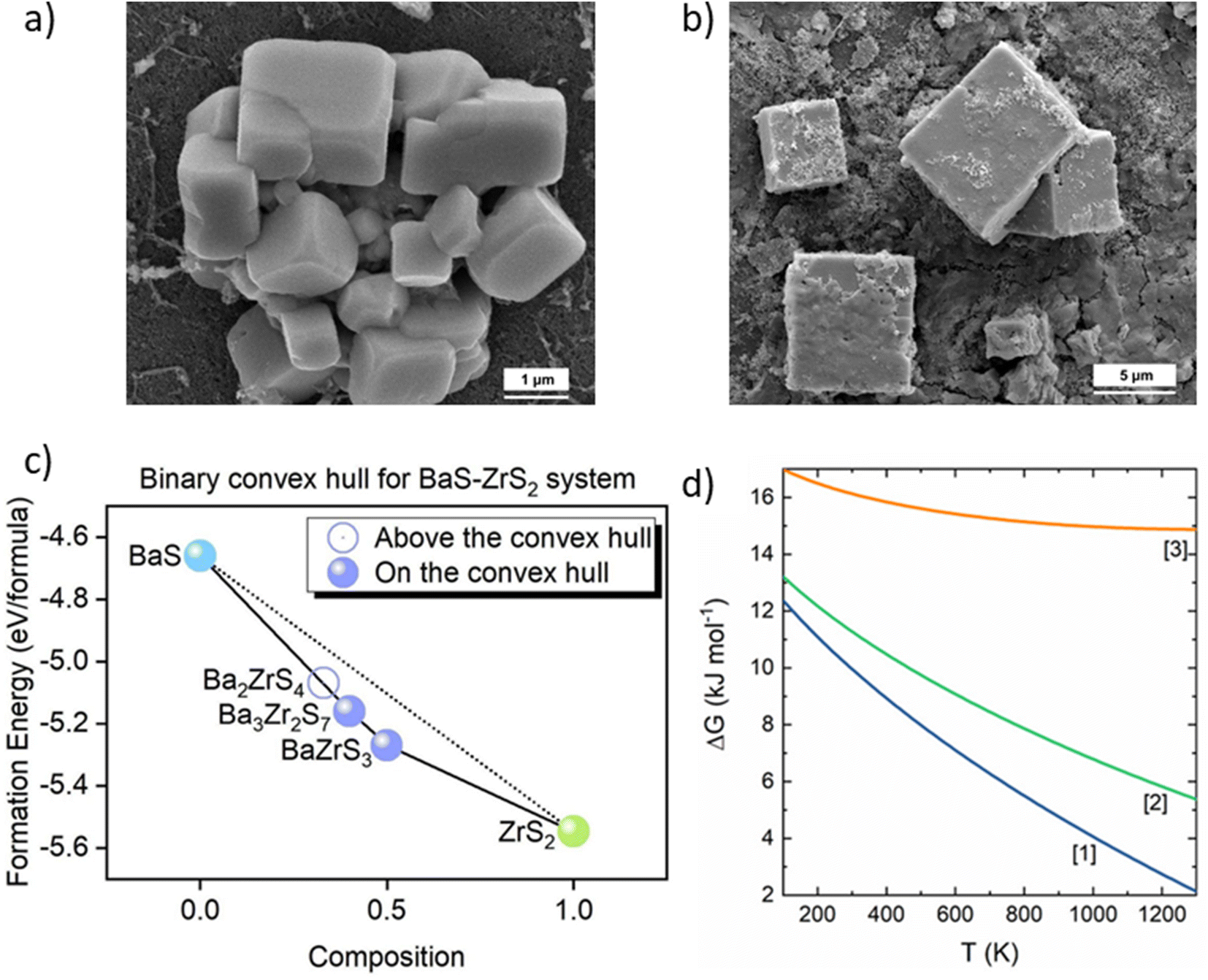 | ||
| Fig. 13 Uncontrolled growth of crystals synthesized from solution-processing routes and phase stability of BaZrS3. Scanning electron microscope image of BaZrS3 synthesized from (a) a mixed slurry of BaS–ZrS3 and (b) bilayer stack of BaS–ZrS3 and sulfurized in the presence of HfH2–sulfur at 575 °C. (a) and (b) Reproduced with permission.105 Copyright 2024, Royal Society of Chemistry. (c) Binary convex hull for the BaS–ZrS2 system. (c) Reproduced with permission.48 Copyright 2023, Wiley. (d) Gibbs free energy (ΔG) plotted as a function of temperature. ΔG is calculated for the decomposition of BaZrS3 into: (1) Ba4Zr3S10 and ZrS2; (2) Ba3Zr2S7 and ZrS2; (3) Ba2ZrS4 and ZrS2. For comparison, all materials are assumed to be in the I4/mmm phase. (a) Reproduced with permission.120 Copyright 2023, Elsevier. | ||
2.2.2.1. Role of sulfur pressure. BaSx/BaS3 liquid flux has been a crucial intermediate in lowering the synthesis temperatures of BaZrS3. However, achieving these liquid fluxes requires maintaining a significantly high sulfur pressure. Our group's previous work has reportedly used around 1 bar of sulfur pressure to form in situ liquid flux during the synthesis of BaZrS3 from either binary sulfide powders or a molecular precursor film.101 Kayastha et al. also confirmed through their calculations that high sulfur pressure in this range is necessary to obtain the BaS3/BaSx phase.121 As synthesis pressures decrease, the crystallinity of the ternary material diminishes, as evidenced by the FWHM of the 〈121〉 peak. Reducing the sulfur pressure below 0.3–0.4 bar results in a mixture of BaZrS3 and Ruddlesden–Popper phases (predominantly Ba3Zr2S7), regardless of the starting Ba
![[thin space (1/6-em)]](https://www.rsc.org/images/entities/char_2009.gif) :Zr ratio. This phenomenon is explained by the limited presence of a liquid flux at these low pressures, leading to a sluggish reaction and metastable intermediate Ruddlesden–Popper phases at temperatures below 600 °C. At even lower sulfur pressures, binary sulfides remain unreacted.101 Kayastha et al. and Han et al. also suggested that at high temperatures, BaZrS3 and Ruddlesden–Popper phases have similar Gibbs free energies of formation, potentially resulting in a mixture of these phases regardless of the initial Ba:Zr ratios48,120 Han et al. demonstrated that Ba3Zr2S7 and BaZrS3 lie on the convex hull, indicating their stability (see Fig. 13c).48 Previously, Li et al. also showed that Ba3Zr2S7 is the most stable Ruddlesden–Popper phase in the Ba–Zr–S system.27 However, Kayastha et al. found that Ba4Zr3S10 has the lowest formation energy among all the Ruddlesden–Popper phases (shown in Fig. 13d). They confirmed this by mixing binary sulfides and heating them together at 900 °C for 5 days, showing that a mixture of BaZrS3 and Ba4Zr3S10 formed irrespective of the metal ratios.120 These Ruddlesden–Popper phase impurities can become a bottleneck due to their similar X-ray diffraction patterns to BaZrS3. Therefore, a secondary structural characterization technique, such as Raman spectroscopy, needs to be employed. This discussion underscores the need to maintain sufficiently high sulfur pressure during synthesis to achieve rapid synthesis and avoid the formation of Ruddlesden–Popper phases. However, high sulfur pressure could also result in the formation of sulfur interstitials, which have been shown to be low-energy deep defects for BaZrS3.122
:Zr ratio. This phenomenon is explained by the limited presence of a liquid flux at these low pressures, leading to a sluggish reaction and metastable intermediate Ruddlesden–Popper phases at temperatures below 600 °C. At even lower sulfur pressures, binary sulfides remain unreacted.101 Kayastha et al. and Han et al. also suggested that at high temperatures, BaZrS3 and Ruddlesden–Popper phases have similar Gibbs free energies of formation, potentially resulting in a mixture of these phases regardless of the initial Ba:Zr ratios48,120 Han et al. demonstrated that Ba3Zr2S7 and BaZrS3 lie on the convex hull, indicating their stability (see Fig. 13c).48 Previously, Li et al. also showed that Ba3Zr2S7 is the most stable Ruddlesden–Popper phase in the Ba–Zr–S system.27 However, Kayastha et al. found that Ba4Zr3S10 has the lowest formation energy among all the Ruddlesden–Popper phases (shown in Fig. 13d). They confirmed this by mixing binary sulfides and heating them together at 900 °C for 5 days, showing that a mixture of BaZrS3 and Ba4Zr3S10 formed irrespective of the metal ratios.120 These Ruddlesden–Popper phase impurities can become a bottleneck due to their similar X-ray diffraction patterns to BaZrS3. Therefore, a secondary structural characterization technique, such as Raman spectroscopy, needs to be employed. This discussion underscores the need to maintain sufficiently high sulfur pressure during synthesis to achieve rapid synthesis and avoid the formation of Ruddlesden–Popper phases. However, high sulfur pressure could also result in the formation of sulfur interstitials, which have been shown to be low-energy deep defects for BaZrS3.122
Moreover, our group's research shows that BaZrS3 does not decompose into binary compounds under sulfur pressures up to 1 bar.101 We also demonstrated that ZrS3 can be used as a starting precursor for the synthesis of BaZrS3 rather than being considered a decomposition product. Additionally, Kayastha et al.'s first-principles calculations predict that BaZrS3 would not decompose into sulfur-rich binaries at sulfur pressures up to at least 100 bar.121
2.2.2.2. Challenges with molecular precursor routes for BaMS3 compounds. Our group recently summarized the key challenges in the low-temperature, solution-processed synthesis of BaMS3 compounds.123 While we have successfully synthesized BaMS3 compounds using fully dissolved molecular precursor inks and incorporating a second sulfurization step in a controlled sulfur environment, a gap remains in achieving grain nucleation directly after annealing the film on a hotplate. Several factors may hinder this, including excessive carbon, trace amounts of oxygen leading to the formation of amorphous metal oxysulfides, premature breakdown of metal–sulfur complexes forming an amorphous Ba–M–S sulfide matrix, or rapid solvent evaporation causing premature nucleation of metal–sulfur complexes, which also result in an amorphous Ba–M–S sulfide matrix.
To address these issues, we developed the H2S–HfS3 oxygen shuttle-sink system to remove oxygen from the film during sulfurization. However, maintaining sufficient sulfur pressure is crucial to ensure phase-pure BaZrS3 synthesis, as inadequate pressure can lead to Ruddlesden–Popper phase impurities. Additionally, the use of a liquid flux in low-temperature BaMS3 synthesis has been effective in reducing mass transfer barriers and promoting crystal growth, but it has also led to uncontrolled, randomly oriented micron-sized grains with planar defects. This rapid growth can result in the entrapment of oxide impurities within the crystals. Controlling grain growth remains a key challenge that requires strategic approaches.
Furthermore, substrate selection plays a critical role, as glass substrates often release cationic species during prolonged sulfurization, potentially leading to secondary phases in the film. While quartz may seem appealing, it presents the opposite issue, as cations can diffuse into the quartz during annealing, as observed with Ba diffusion. Finally, while our H2S–HfS3 system effectively removes oxide impurities, it is less efficient in the presence of excessive moisture, as it interferes with the capacity of H2S–HfS3 system to remove oxygen present in the film. Therefore, careful handling is necessary to prevent moisture exposure to samples or ampoules before sulfurization.
Addressing these challenges is essential for developing high-efficiency optoelectronic devices from solution-processed BaMS3 compounds.
The initial instance of nanoparticle synthesis within the chalcogenide perovskite family involved the synthesis of BaTiS3 nanoparticles utilizing reactive metal organoamide precursors. BaTiS3 is known for its quasi-1D hexagonal structure, exhibiting distinct properties like optical anisotropy, mid-IR birefringence, and thermal transport characteristics.30,91,130–132 Zilevu et al. indicated that controlling the morphology (nanoparticle versus nanorod) could be achieved by alternating between heat-up and hot injection methods during crystal growth (see Fig. 14a and b). Furthermore, size regulation was attainable by adjusting reaction time and temperature, with a hot injection reaction at 360 °C yielding nanorods with an aspect ratio of 8:1 (50 nm length, 6 mm width). Reactions were conducted in oleylamine, which with a boiling point of 364 °C, provides a broad reaction temperature range. Although not explicitly demonstrated, the ligand on the nanoparticle surface may also influence the process. Oleylamine's π bond in its chain prevents chain folding and stacking, thereby averting agglomeration and facilitating stable suspensions.133 To avoid undesired by-products, they employed reactive Ba[N(SiMe3)2]2(THF)2 and Ti(NMe2)4 metal precursors, combined with oleylamine and N,N′-diethylthiourea as the sulfur source. While testing various sulfur sources, such as elemental sulfur, carbon disulfide, thioacetamide, and different thioureas, nanocrystals were found to most readily synthesize with thioureas, known for their decomposition upon heating and liberation of H2S, interacting with the metal precursors to form the desired compounds. Maintaining reaction conditions devoid of water, oxygen, or any oxygen-containing ligands was emphasized to prevent oxide impurity formation. In heat-up reactions, metal precursors, N,N′-diethylthiourea, and oleylamine were added to the reaction vessel and then heated to 360 °C. Conversely, for hot injection reactions, metal precursors and oleylamine were heated to 360 °C, while a preheated N,N′-diethylthiourea, and oleylamine solution at 60 °C was injected into the reaction vessel. Despite testing different reaction temperatures, crystalline BaTiS3 was not achieved below 290 °C. However, the pXRD pattern of the synthesized nanorods slightly deviated from the reported bulk XRD pattern due to potential sulfur deficiency, resulting in a partial off-stoichiometric phase with a commensurate structure.124 This structure, resembles that of SrxTiS3, which features two interpenetrating subcells based on TiS3 and Sr lattices, causing additional peaks in the diffraction pattern and shifting the main peaks.134 A clear difference in the morphology of BaTiS3 nanoparticles grown using two different methodologies is evident in Fig. 14c–e. Notably, the synthesized nanoparticles exhibited sufficient stability in air but degraded rapidly in water, potentially limiting their utility in water-based applications. Nevertheless, their air stability offers promise for utilization in optoelectronic applications.
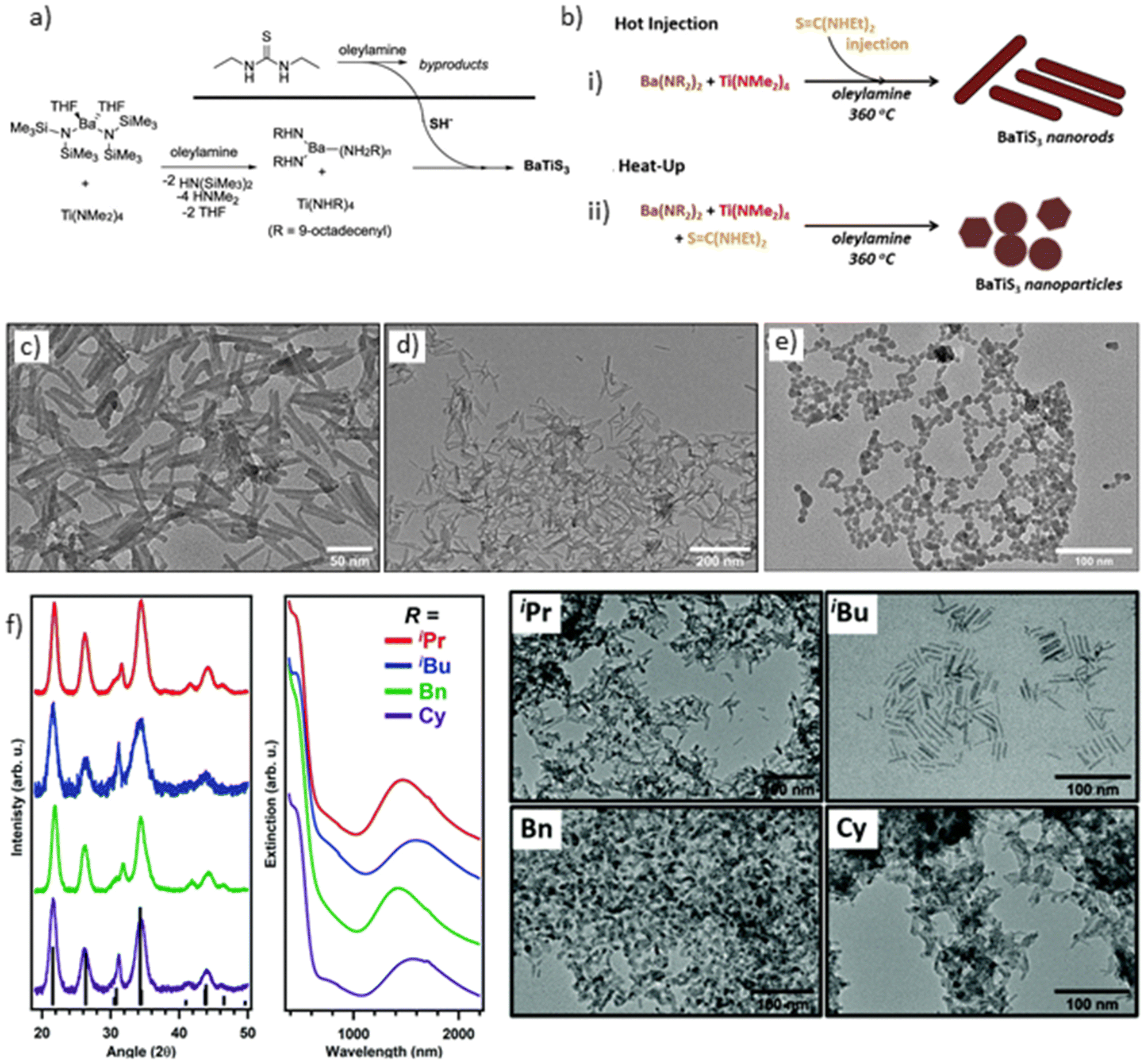 | ||
| Fig. 14 BaTiS3 nanoparticles synthesis. (a) Reaction scheme for the synthesis of BaTiS3 nanoparticles, (b) reaction conditions employed for the hot injection and heat-up synthesis of BaTiS3 nanoparticles, (c) and (d) TEM images of nanoparticles synthesized using the hot injection method, (e) TEM image of nanoparticles synthesized using the heat-up method, (f) X-ray diffraction pattern and TEM images of BaTiS3 nanoparticles synthesized from barium dithiocarbamate precursors with varying alkyl chains. (a)–(e) Reproduced with permission.124 Copyright 2021, American Chemical Society. (f) Reproduced with permission.125 Copyright 2021, Royal Society of Chemistry. | ||
Ingram et al. reported the synthesis of BaTiS3 nanoparticles using single-phase precursors of barium and titanium dithiocarbamates.125 The synthesis began with the preparation of barium N,N-dialkyl dithiocarbamate by forming a dithiocarbamate ion solution in water/ethanol through the combination of dialkylamine and carbon disulfide, followed by the addition of pure barium metal chunks. After stirring at room temperature for 30 minutes, the mixture was heated to 350 °C for 30 minutes (where alkyl groups = isopropyl, isobutyl, benzyl, cyclohexyl), barium dialkyl dithiocarbamate formed in the solution. Subsequently, crystals were recrystallized by adding ether/tetrahydrofuran and dried under vacuum at 80 °C to eliminate moisture and obtain anhydrous barium dithiocarbamate. Titanium dithiocarbamate species were obtained by introducing carbon disulfide to Ti(NiPr2)4, where carbon disulfide was inserted into the metal–amide bond to form dithiocarbamate species. The resulting barium and titanium dithiocarbamate precursors were co-added in a 2:1 molar ratio in an oleylamine solution and heated to 350 °C to produce BaTiS3 nanocrystals (see Fig. 14f). It was observed that excess Ba precursor was crucial for obtaining phase-pure BaTiS3 nanocrystals and preventing TiS2 impurities. However, the resulting nanorods exhibited poorer crystallinity compared to nanoparticles synthesized by Zilevu et al. The exact cause of this phenomenon is not fully understood but could stem from inherent impurities during barium dithiocarbamate synthesis, or the decomposition temperature of barium dithiocarbamate may not align with the ideal conditions for ternary BaTiS3 synthesis. Additionally, some pXRD peaks were slightly shifted compared to the diffraction spectra of bulk BaTiS3, indicating a sulfur-poor composition. While this method utilizes direct single-source precursors for BaTiS3 synthesis, it offers less control over material properties compared to the hot-injection method previously developed by Zilevu et al. Nonetheless, this approach may hold promise for synthesizing BaZrS3 nanocrystals.125
While BaZrS3 has emerged as one of the most extensively studied chalcogenide perovskites, limited attention has been devoted to the direct nanoparticle synthesis of BaZrS3, with only two reports available in the literature. Furthermore, both studies encountered challenges in producing colloidally stable nanoparticles, preventing the fabrication of BaZrS3 films using such nanoparticles. The primary hurdle lies in effectively utilizing reactive metal precursors while maintaining oxygen and moisture-free conditions during synthesis. Addressing these challenges, Yang et al. employed metal dithiocarbamate precursors for BaZrS3 nanoparticle synthesis. Barium dibutyl dithiocarbamate was synthesized from the reaction of Ba(OH)2 with carbon disulfide and dibutylamine, while zirconium diethyldithiocarbamate was obtained by reacting ZrCl4 with diethylamine and carbon disulfide. These dithiocarbamates were then added to oleylamine in a 1:1 metal ratio at a total concentration of 0.488 M. No additional sulfur source was necessary, as the thermal decomposition of the dithiocarbamates yielded metal–sulfur monomers. The solution was heated to 330 °C and maintained for 18 hours to form BaZrS3 nanocrystals (shorter reaction times of 30 minutes also resulted in BaZrS3 nanocrystals). However, their powder X-ray diffraction (pXRD) pattern exhibited multiple impurity peaks that did not correspond to the perovskite crystal structure, which were attributed to zirconium-rich regions and oxide impurities (see Fig. 15a).135 The TEM images reveal agglomerates of nanoparticles rather than distinct, isolated particles, indicating that the nanoparticles did not disperse well in the solution (shown in Fig. 15b). The lattice spacing observed in the HRTEM image corresponded to BaZrS3 (illustrated in Fig. 15c). Without STEM-EDX measurements, confirming the presence of zirconium-rich regions in the nanoparticles remains challenging, necessitating further investigation to accurately assign these peaks. Conversely, tighter control over oxygen and moisture exposure during nanoparticle synthesis could mitigate oxide impurities.
 | ||
| Fig. 15 BaZrS3 nanoparticles synthesis. (a) X-ray diffraction pattern of BaZrS3 nanoparticles synthesized from metal dithiocarbamate precursors, (b) and (c) TEM and HRTEM images of BaZrS3 nanoparticles synthesized by Yang et al.,135 (d) reaction conditions used by Zilevu et al.136 for synthesizing BaZrS3 nanoparticles, (e) TEM image of the synthesized nanoparticles, (f) procedure for capping ligands on solid-state synthesized BaZrS3 nanoparticles, (g) TEM image of BaZrS3 nanoparticles synthesized by Ravi et al.65 (a)–(c) Reproduced with permission.135 Copyright 2022, American Chemical Society. (d) and (e) Reproduced with permission.136 Copyright 2022, Royal Society of Chemistry. (f) and (g) Reproduced with permission.65 Copyright 2021, Royal Society of Chemistry. | ||
Similar to Yang et al., Zilevu et al. also synthesized BaZrS3 nanoparticles, albeit using different precursors and sulfur sources. However, they encountered similar challenges with extra peaks in the diffraction pattern. Their method involved utilizing Ba[N(TMS)2]2(THF)2 and Zr[N(CH3)2]4 as the metal precursors, along with N,N-diethyl thiourea as the sulfur source. These precursors were combined in a 1:2:60 mole ratio to the dried oleylamine (shown in Fig. 15d). The reaction mixture was then heated to the desired temperature and maintained for 30 minutes. They observed additional peaks in the nanoparticles synthesized at temperatures around 275 °C, which they attributed to a low-temperature phase. Upon increasing the reaction temperature to 365 °C, they observed BaZrS3 nanoparticles without structural distortions, indicating a high-temperature phase.136 However, they encountered difficulties in consistently reproducing the high-temperature reaction. Variability in critical synthesis parameters, potentially due to the use of home-built setups relying on heating tape for temperature control, may contribute to this inconsistency. Thus, tighter control of synthesis parameters is necessary to ensure reproducibility when incorporating these nanoparticles into optoelectronic devices. Consistent with Yang et al., they also observed significant agglomeration of the nanoparticles, indicating poor dispersion (see Fig. 15e). Notably, Zilevu et al. found that the synthesized nanoparticles exhibited reasonable stability in air and water.136
Recently, our group published a study demonstrating a solution-based method for synthesizing impurity-free BaZrS3 nanoparticles.137 These nanoparticles exhibited no additional unassigned peaks previously observed by Zilevu et al.136 and Yang et al.135 using heat-up synthesis method. While Yang et al.135 attributed the extra peaks to impurities, Zilevu et al.136 suggested that nanoparticles synthesized below 365 °C represented a distinct phase of BaZrS3, which they termed low-temperature BaZrS3. In our study, commercially available cyclopentadienyl barium and tetrakisethylmethylamido zirconium were utilized as zirconium precursors. During the standard heating procedure, these precursors were added to a round-bottom flask and reacted with a tenfold molar excess of CS2 to form metal–sulfur-bonded intermediates. Subsequently, oleylamine was introduced as both a coordinating solvent and reaction medium. A portion of the oleylamine also reacted with the excess CS2 in the flask to form oleyldithiocarbamate species. Heating this system to temperatures between 290–340 °C under a constant flow of argon yielded BaZrS3 nanoparticles with additional peaks, similar to those previously reported in the literature. To address this issue, we hypothesized that rapid heating of the metal–sulfur-bonded precursors to temperatures significantly higher than 340 °C could produce phase-pure BaZrS3 nanoparticles. To test this hypothesis, a hot-injection method was developed, marking the first application of this approach in the synthesis of chalcogenide perovskites. Using oleylamine as the primary solvent posed a challenge, as its excessive refluxing limited the reaction temperature to approximately 340 °C. To overcome this, mineral oil, consisting of long-chain alkanes, was employed, enabling the system to reach temperatures as high as 375 °C. For the hot-injection synthesis, mineral oil was used as the bulk solvent in the reaction flask and heated to 370–375 °C. Once the temperature stabilized, a slurry containing organobarium and metal–organic zirconium precursors in excess CS2 and oleylamine was introduced into the flask via a Merlic adapter. This hot-injection method successfully and reproducibly synthesized phase-pure BaZrS3 nanoparticles at the lowest temperature reported in the literature. This breakthrough opens new avenues for exciting applications of BaZrS3.
The same method was applied to synthesize BaHfS3 nanoparticles. However, similar to earlier reports for BaZrS3, the BaHfS3 nanoparticles exhibited additional diffraction peaks, suggesting that a reaction temperature of 375 °C might still be insufficient for achieving phase-pure BaHfS3. While we also synthesized other chalcogenide perovskites, such as α-SrZrS3 and α-SrHfS3, these materials fall outside the scope of this work. Readers are encouraged to consult our publication for further details.
Ravi et al. previously achieved a significant advancement by synthesizing BaZrS3 nanocrystals at 600 °C using the I2 flux method initially developed by Niu et al. They functionalized the nanocrystal surfaces with N-methyl-2-pyrrolidinone to create a colloidally stable nanocrystal ink. Additionally, they capped the nanocrystals with non-polar oleylamine, resulting in a stable dispersion in chloroform (shown in Fig. 15f). The TEM image in Fig. 15g displays cubic crystals on the nanometer scale. This stable ink in chloroform was then used to coat a thin film of BaZrS3, demonstrating a functional field-effect transistor.65
Although substantial advancements have been achieved in synthesizing BaZrS3 and hexagonal BaTiS3 nanoparticles, further efforts are necessary to establish their colloidal stability in benign solvents. Additionally, exploring ligand exchange methods could enhance the attachment of desirable organic or inorganic ligands onto the surface of the nanoparticles. Efforts should be made to synthesize nanoparticles from cost-effective metal precursors such as metal acetylacetonates and metal halides. However, this process pose challenges due to the strong affinity of early transition metals for oxygen and alkaline earth metals for halides. Ravi et al.65 reported attempts to synthesize BaZrS3 nanoparticles from metal acetylacetonate and metal halide precursors but were unsuccessful in achieving ternary phases. Nonetheless, developing specific traps in solution that selectively react with these impurities could enable the phase-pure synthesis of ternary chalcogenides and should be pursued.
To address this issue, Comparotto et al. co-sputtered Ba–Zr onto a molybdenum deposited silicon substrate and capped the film with a 100 nm thick SnS layer to prevent oxidation before sulfurization in a flow-tube furnace. Surprisingly, they synthesized BaZrS3 film at 590 °C with sulfur pressures between 2–4 Pa within 20 minutes, achieving high crystallinity as measured by the FWHM of the 121 XRD peak.138 This contrasts with Vincent et al., who reported the need for high sulfur pressures (>0.4 bar) for high crystallinity, attributing the success to the presence of BaSx liquid flux.101
Comparotto et al. speculated that they achieved an intermediate flux, such as BaS3, which reduced diffusion barriers and accelerated kinetics. However, given the low pressures used, it is unlikely they achieved BaS3.104 They also suggested that the absence of metal–sulfur bonds in their precursor film provided an alternative nucleation pathway compared to metal–sulfur bonded precursor films.
Interestingly, their synthesis method, possibly due to lower sulfur pressures, allowed the molybdenum back contact to survive, forming only a thin layer of MoS2, thereby potential opening the door for solar cells and other optoelectronic devices using this approach. Further research into the reaction mechanism of this method is needed to enable its application to other synthesis techniques.
2.3. Film morphology and composition
Achieving a smooth, well-oriented film with a homogeneous composition and no secondary phases is crucial for synthesizing high-performance devices. Although BaZrS3 films synthesized using CS2 sulfurization of oxide precursor films have shown reasonable continuity with thicknesses ranging from 200 to 500 nm, they have been deposited on non-conductive substrates, limiting their applicability. Additionally, Gupta et al. observed that their sulfurized films exhibited relatively low crystallinity, with grains embedded in an amorphous matrix.62 Similarly, Sharma et al., Wei et al., Han et al., and Xu et al., employing similar sulfurization methods, confirmed the presence of significant oxide impurities on the surface, with species bonded to sulfur and oxygen (S–O) (see Fig. 16a–c).48,57,86,92,140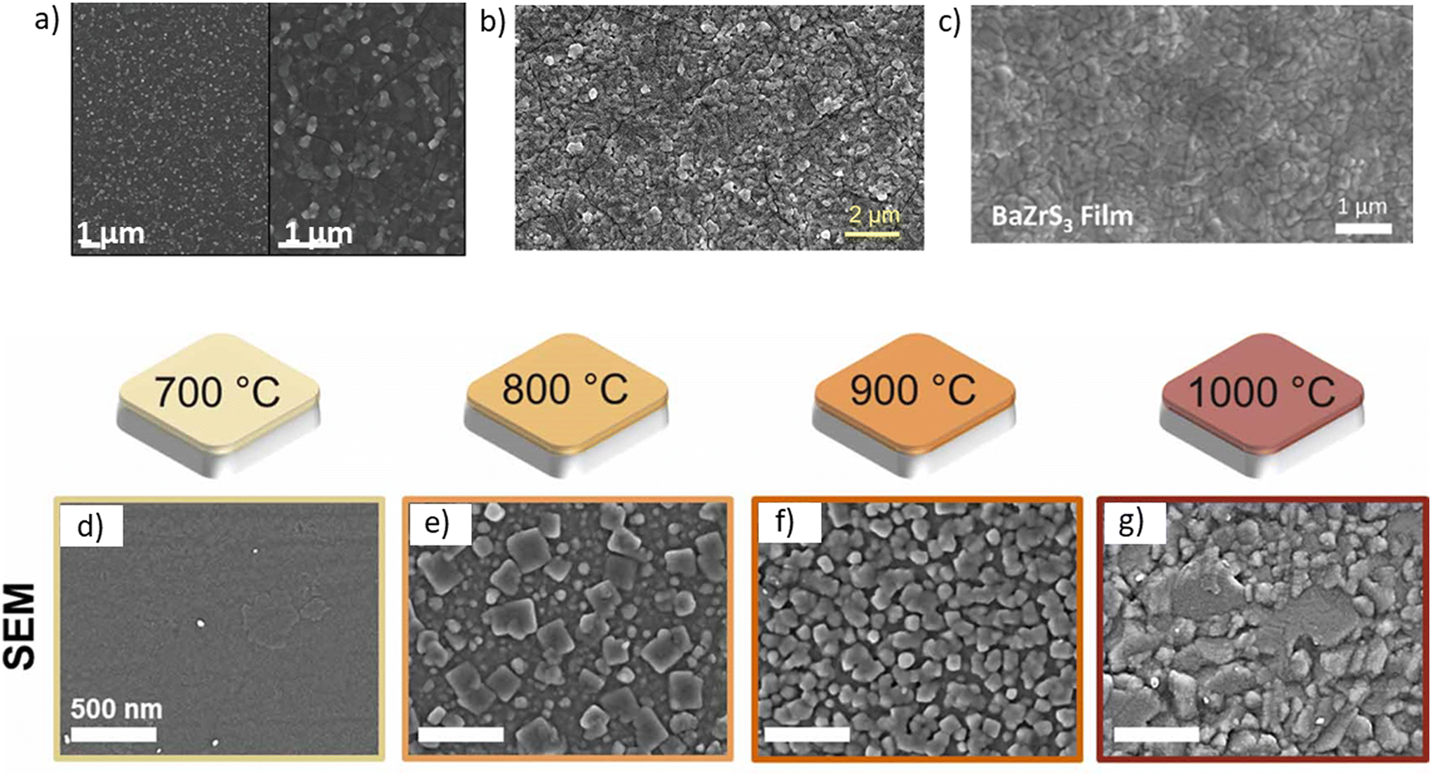 | ||
| Fig. 16 Morphology of BaZrS3 films synthesized using various methods: (a) Gupta et al.62via CS2 sulfurization of an oxide precursor film, (b) Han et al.48 using magnetron sputtering from a BaZrS3 target followed by annealing, (c) Sharma et al.92 through CS2 sulfurization of an oxide precursor film, and (d)–(g) Ramanandan et al.95via H2S sulfurization of an oxide precursor film. (a) Reproduced with permission.62 Copyright 2020, Wiley. (b) Reproduced with permission.48 Copyright 2023, Elsevier. (c) Reproduced with permission.92 Copyright 2023, American Chemical Society. (d)–(g) Reproduced with permission.95 Copyright 2023, IOP Science. | ||
Márquez et al. used H2S to sulfurize oxide precursor films, noting a gradual increase in sulfur incorporation with increasing sulfurization temperature. However, the S/(S + O) ratio plateaued at 0.85 at 1000 °C, indicating the presence of substantial oxygen impurities. Despite containing closely packed grains with sizes around 100 nm, the annealed films exhibited cracks, attributed to thermal expansion mismatch between the BaZrS3–BaZrO3 film and the quartz substrate.68 Ramanandan et al. followed up on Márquez et al.'s film deposition method and found that all sulfurized samples were Zr-rich and Ba-poor, with sulfur content increasing with temperature. They also observed higher sulfur content on the film surface than the bulk due to the diffusion limitation of sulfur-containing species. Unfortunately, the films displayed a Ba–S–O phase in the top layer, a common occurrence in BaZrS3 films derived from oxide precursor sulfurization. Nonetheless, films produced using this method appeared relatively continuous and densely packed (shown in Fig. 16d–g).95
Comparotto et al. reported around 4% oxygen in the bulk of BaZrS3 film, with a nearly stoichiometric Ba:Zr composition. Fig. 17a illustrates their hypothesis regarding the occurrence of oxygen contamination during the synthesis steps.97 Mukherjee et al. conducted detailed compositional measurements on similarly rapid annealed films, noting compositional fluctuations near the surface, including various sulfur-containing species such as BaSO3 and BaSO4.141 Riva et al. utilized Al K-α and Ga K-α X-rays to probe different film depths, identifying a BaSO4 and Zr–O-rich layer up to a depth of 3 nm, followed by a Zr–O-rich layer up to a depth of 15 nm (see Fig. 17b).139 Comparotto et al. also observed compositional fluctuations in their Sn-capped BaZrS3 film.138
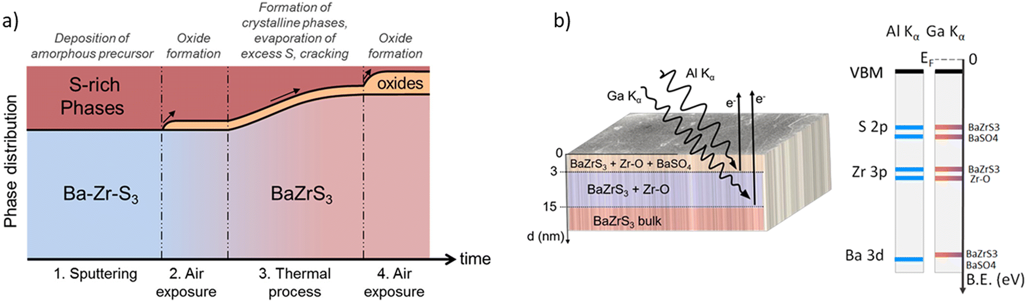 | ||
| Fig. 17 Surface oxide impurities in BaZrS3. (a) Schematic representation of phase distribution in the BaZrS3 film over time upon exposure to air. (a) Reproduced with permission.97 Copyright 2020, American Chemical Society. (b) Schematic illustrating the different phases present in the near-surface layers, as identified by hard X-ray photoelectron spectroscopy. (b) Reproduced with permission.139 Copyright 2024, American Chemical Society. | ||
While detailed compositional analysis has not yet been conducted for low-temperature solution-processing methods, these samples indicate compositional fluctuations and non-stoichiometric compositions. Across all BaZrS3 synthesis methods, challenges persist with substantial oxide impurities at the surface, notable oxygen content in the bulk, and significant compositional fluctuations and non-stoichiometries throughout the film. These issues may stem from the high oxophilicity of Zr, Ba's tendency to form stable sulfite and sulfate species, and mass transfer limitations during film growth. Grain size and composition vary depending on the method: solution-processing methods that rely on excess sulfur to access BaSx flux have produced relatively large cubic grains (>1 μm). At the same time, CS2 and H2S sulfurized films exhibit more modest grain sizes. Controlling the composition is essential, as insufficient precision can lead to unwanted defects and impact film properties; addressing these issues is critical. Etching away a few layers from the film may help mitigate surface contaminants, but careful handling is necessary to avoid further contamination from the etchant.
Our group recently demonstrated that BaZrS3 can accommodate barium-poor off-stoichiometric compositions similar to other chalcogenides, such as Cu(In,Ga)Se2. Binary sulfide powders were mixed in various molar ratios with elemental sulfur and heated to a constant temperature of 575 °C for 12 hours. No secondary phases were observed up to a Ba:Zr ratio of 0.7. Secondary impurities of ZrS3 were observed for Ba:Zr ratios lower than 0.7. As expected, the BaS3 secondary phase was observed for Ba:Zr ratios greater than 1. Since BaS3 is water-soluble, a gentle water wash dissolved away the secondary phase, resulting in phase-pure BaZrS3. Thus, phase-pure BaZrS3 is attainable for Ba:Zr ratios greater than 0.7.105 However, the different compositions may have implications on the electronic and optoelectronic properties of BaZrS3, which need further study.
Table 1 summarizes the synthesis conditions for all film deposition methods used to prepare BaZrS3.
| Synthesis method | Annealing temp (°C) | Annealing time | Annealing atmosphere | Substrate used | References |
|---|---|---|---|---|---|
| Reactive co-sputtering of Ba–Zr–S precursor films at ambient temperature followed by a thermal treatment to induce crystallization | 900 | 1 min | Ar | Si wafer | Comparotto et al.97 |
| Polymer-assisted aqueous solution of metal precursors was spincoated followed by sulfurization in a mixed CS2 and Ar atmosphere | 900 | 3 h | CS2 + Ar | Sapphire | Dhole et al.94 |
| CS2 sulfurization of solution deposited BaZrO3 film | 1050 | 4 h | CS2 + N2 | Quartz | Gupta et al.62 |
| Magnetron sputtering from the synthesized BaZrS3 target followed by annealing | 1000 | 1–16 h | CS2 | Quartz | Han et al.48 |
| PLD deposited Ba–Zr–O films were annealed at temperatures between 700 and 1100 °C under a continuous flow of H2S gas (5%) | 900–1000 | 30 min | H2S + Ar | Quartz | Márquez et al.68 |
| Doctor blade coating of soluble mixed precursor ink utilizing CS2 insertion chemistry followed by sulfurization of film in an ampule | 575 | 20 min–16 h | Sulfur + HfH2 | Eagle XG glass | Pradhan et al.117 |
| Coating of colloidal BaZrS3 nanocrystals ink in chloroform followed by annealing | 150–250 | 20 min | N2 | Si wafer | Ravi et al.65 |
| Drop cast of hybrid precursor ink followed by sulfurization of film in an ampule | 575 | 2 h | Sulfur | Al2O3 coated Eagle XG glass | Turnley et al.74 |
| Epitaxial growth using pulsed laser deposition on LaAlO3 | 700–850 | Ar + H2S | LaAlO3/SrLaAlO4 | Surendran et al.72 | |
| Sputter Ba–Zr, capped with SnS followed by sulfurized in sulfur environment | 600 | 20 h | Sulfur | Mo/Si | Comparotto et al.138 |
| Molecular beam epitaxial growth | 900 | H2S | LaAlO3 | Sadeghi et al.89 | |
| CS2 sulfurization of PLD deposited BaZrO3 films | 900–1050 | 4 h | CS2 + H2/N2 | Sapphire | Wei et al.86 |
| CS2 sulfurization of PLD deposited amorphous Ba–Zr–S films | 500–900 | 2–8 h | CS2 + Ar | Sapphire | Yu et al.93 |
| Sputter deposit a stack of BaS/Zr on SiC followed by sulfurization | 1000–1050 | Sulfur | SiC | Jamshaid et al.99 | |
| Solution deposit a stack of BaS/ZrS3 followed by sulfurization | 575 | 2 h | Sulfur + HfH2 | Al2O3 coated Eagle XG glass | Vincent et al.105 |
| Doctor blade coat a mixed precursor ink of BaS and ZrS3 followed by sulfurization | 575 | 2 h | Sulfur + HfH2 | Al2O3 coated Eagle XG glass | Vincent et al.105 |
3. Properties of BaMS3 compounds
3.1. Defect chemistry
To successfully implement BaZrS3 as a solar absorber in solar cells, it is crucial to understand its defect chemistry. This knowledge can guide the selection of dopants, influencing the conductivity type, carrier concentrations, and identifying deep defects that could hinder the performance of solar cells. Regarding BaZrS3, three studies have reported on its defect chemistry, all using the HSE06 hybrid functional but with different Hubbard U values and supercell sizes.122,142,143 Despite these variations, all studies agree that sulfur vacancies are the predominant shallow donor defects in BaZrS3, characterized by low formation energies. These low formation energies may result in high electron concentrations under sulfur-poor growth conditions.The defect calculations included intrinsic point defects such as vacancies (VBa, VZr, and VS), antisites (BaZr, ZrBa, BaS, SZr, SBa, ZrS), and interstitials (Bai, Zri, and Si). Yuan et al. suggested that, unlike sulfur vacancies, VBa and BaZr also have shallow acceptor defects, albeit with high formation energies. Under sulfur-rich conditions, the defect formation energy of VS increases while the formation energies of acceptor defects are reduced. Consequently, the Fermi level would be pinned closer to the intersection of VS and VZr, which lies approximately 0.5 eV below the conduction band. Therefore, they argued that intrinsic BaZrS3 will always be n-type, while the carrier concentrations can be modified by the growth conditions. The shallow acceptor defects such as VBa, VZr and BaZr are strongly compensated by the donor defects, and even in the best-case scenario with p-type doping, under sulfur-rich conditions, the Fermi level will be pinned approximately 0.6 eV above the valence band maximum.122
Among the deep defects such as VZr, BaZr, SBa, SZr, and Si, only Si has a low formation energy, especially in sulfur-rich conditions. Therefore, under sulfur-rich conditions, high concentrations of sulfur interstitials are likely, which could lead to deep recombination centers. Fig. 18 summarizes the defect calculations. Yuan et al. further calculated a capture coefficient of 1.25 × 10⁻⁹ cm3 s−1, arguing that it is slightly smaller than the dominant recombination centers of iodine interstitials in CH3NH3PbI3.122
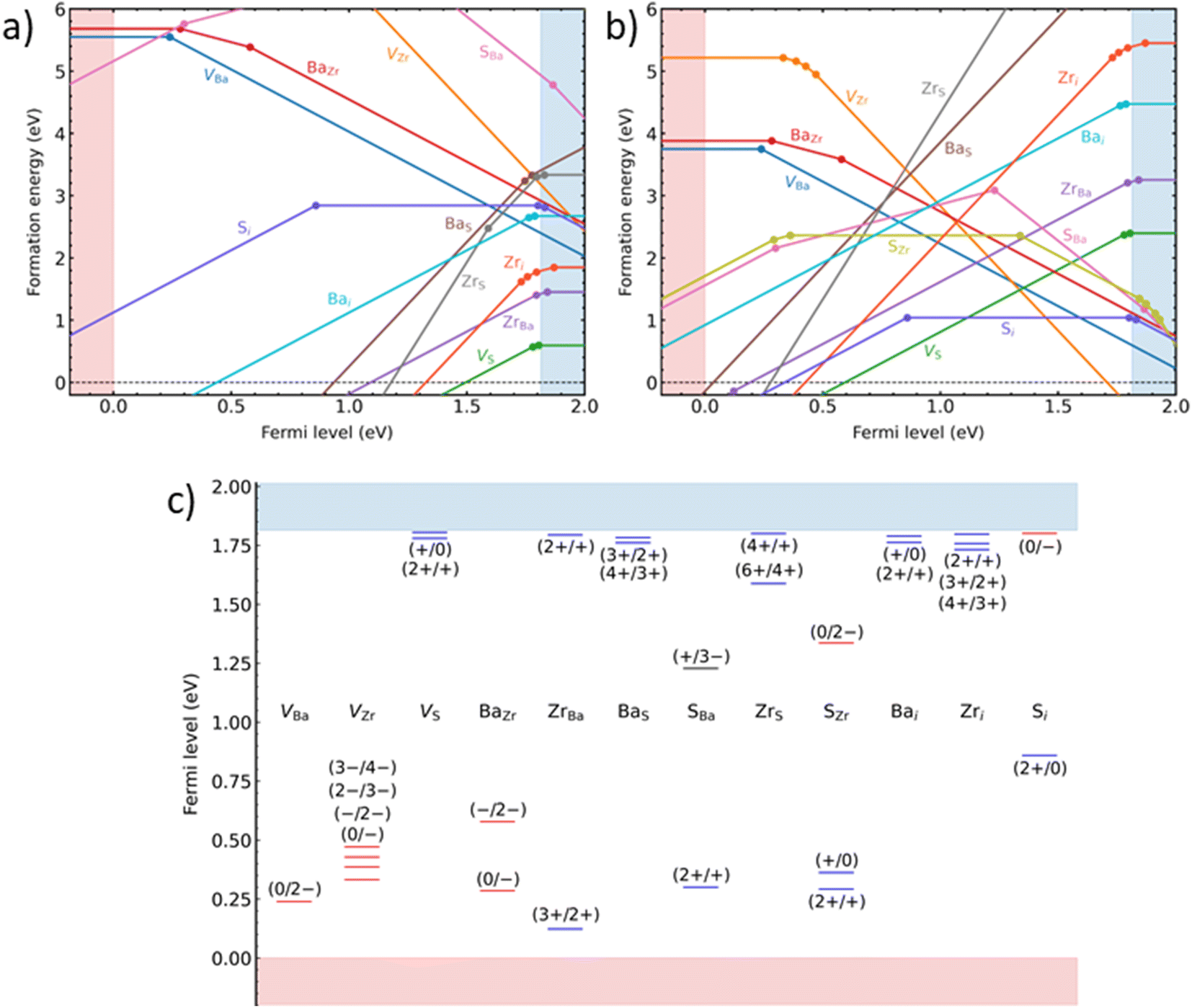 | ||
| Fig. 18 Defect chemistry calculations for BaZrS3. (a) Plot showing the formation energy of various defects as a function of the Fermi level under sulfur-poor conditions. (b) Plot showing the formation energy of various defects as a function of the Fermi level under sulfur-rich conditions. (c) Plot illustrating the charge transition levels of various defects within the forbidden energy region. (a)–(c) Reproduced with permission.122 Copyright 2024, American Physical Society. | ||
In light of the above discussion, it would be advisable to operate under sulfur-poor conditions to achieve a weak n-type character by optimizing the growth conditions for the films and devising a p–i–n architecture. An external p-type dopant, such as La on the Zr site or alkali metals on the Ba site, could also be explored to keep the electron concentration in check while growing BaZrS3 films under sulfur-poor conditions. Oxygen-related defects could be common in BaZrS3 due to the frequent sulfurization of oxide films to synthesize ternary chalcogenides and the high oxophilicity of early transition elements. Interestingly, Yuan et al.'s calculations showed that both Oi and OS are electrically inactive and stable in the neutral charge state across almost the entire Fermi level range.122 Moving forward, it would be valuable to study defect complexes in BaZrS3, as they could have low formation energies and significantly affect the material's intrinsic properties.
3.2. Stability
Chalcogenide perovskites have been proposed as stable alternatives to lead halide perovskites that are known to degrade under heat, air, and moisture. Experimental evidence supports this assertion, with some reports indicating BaZrS3's superior stability compared to halide perovskites. Gupta et al. highlighted BaZrS3's improved luminescence stability over methylammonium lead iodide (MAPbI3) perovskite, as the photoluminescence (PL) of MAPbI3 vanished within 2 weeks of exposure to air, whereas BaZrS3 maintained substantial PL even after 5 weeks, though with some reduction in intensity (see Fig. 19a and b). They emphasized BaZrS3's superior chemical stability by observing that the film's X-ray diffraction (XRD) pattern remained unchanged after 10 weeks in ambient conditions.62 Similarly, Zilevu et al. found no changes in the powder XRD (pXRD) pattern of their synthesized BaZrS3 nanoparticles after 9 weeks of air exposure, indicating robust atmospheric stability even at the nanoscale (shown in Fig. 19c).136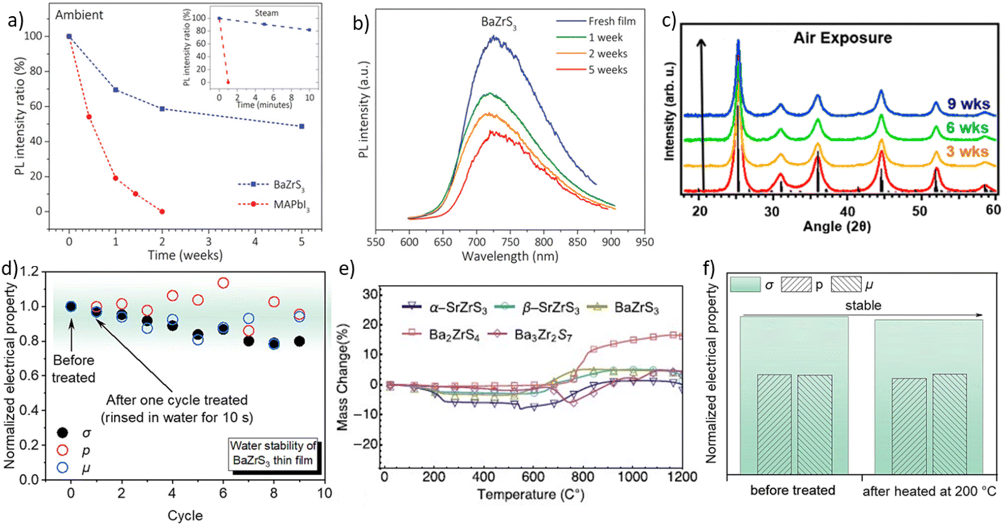 | ||
| Fig. 19 Stability of BaZrS3 against extrinsic factors. (a) Plot comparing the PL intensity of BaZrS3 and MAPbI3 films under ambient conditions over time, with an inset showing the variation in PL intensity upon exposure to steam. (b) Plot depicting the PL intensity of BaZrS3 over several weeks of exposure to ambient conditions. (a) and (b) Reproduced with permission.62 Copyright 2020, Wiley. (c) Plot illustrating the structural stability of BaZrS3 nanoparticles over several weeks in air. (c) Reproduced with permission.136 Copyright 2022, Royal Society of Chemistry. (d) Plot demonstrating the superior water stability of BaZrS3 film by assessing carrier properties after water rinsing. (d) Reproduced with permission.48 Copyright 2023, Elsevier. (e) Plot showing the exceptional thermal stability of BaZrS3 powder up to 500 °C. (e) Reproduced with permission.64 Copyright 2018, Springer Nature. (f) Plot indicating minimal changes in the carrier properties of BaZrS3 after heat treatment at 200 °C. (f) Reproduced with permission.48 Copyright 2023, Elsevier. | ||
In addition to atmospheric stability, BaZrS3 demonstrated greater moisture resistance than MAPbI3, which lost its PL instantly upon exposure to steam, while BaZrS3 maintained its PL for 10 minutes in the presence of steam. Ab initio Molecular Dynamic simulations revealed that BaZrS3 has weak interactions with water, and anion vacancy migration, a significant cause of instability in MAPbI3, is seven orders of magnitude lower in BaZrS3, suggesting photodegradation is not a major concern.62 Han et al. reported strong water stability for BaZrS3 thin films, observing minimal change in electrical conductivity (remaining within 80% of the original value) after 10 cycles of water rinsing (totaling 100 seconds) (shown in Fig. 19d). XRD measurements confirmed the phase stability of BaZrS3.48
Yang et al. rinsed BaZrS3 powder synthesized from BaS3 liquid flux multiple times to remove water-soluble impurities, obtaining a phase-pure XRD pattern for BaZrS3.100 Ravi et al. tested the photocatalytic activity of BaZrS3 nanocrystals (synthesized using an I2 flux) by studying methylene blue degradation in water under sunlight. Their results demonstrated BaZrS3's reasonable photocatalytic activity and water stability. However, they noted that BaZrS3 began to degrade in water after 10–12 hours under light and after a few days in the dark.65 Zilevu et al. also observed their synthesized nanoparticles starting to degrade in water after 30 minutes.136 In summary, BaZrS3 exhibits much greater water stability than lead halide perovskites but still needs to meet the standard for water-based applications.
Eya et al. recently demonstrated the superior stability of BaZrS3 surfaces in the presence of oxygen and moisture through density functional theory (DFT) calculations.144 Their study focused on the three most stable surfaces of BaZrS3: (010), (100), and (111). They found that moisture exhibited only weak interactions with these surfaces, while oxygen, although interacting relatively more strongly, did not significantly alter the electronic properties. Notably, these interactions were predominantly localized at Zr sites, with Ba sites showing no interaction with either moisture or oxygen.
In a solar farm exposed to intense heat, solar panels can reach temperatures of up to 60–80 °C. Therefore, understanding the thermal stability of promising photovoltaic materials is crucial. In this context, Niu et al. conducted thermogravimetric analysis (TGA) and differential scanning calorimetry (DSC) studies to evaluate the stability of BaZrS3 across different temperatures. They found that BaZrS3 remains stable in air up to 650 °C but degrades at higher temperatures into a mixture of BaSO4 and ZrO2 (see Fig. 19e).64 Similarly, Han et al. heated BaZrS3 in air at 200 °C and observed no signs of degradation (illustrated in Fig. 19f).48 Consistent with these findings, Ravi et al. also heated BaZrS3 nanocrystals in air up to 400 °C without detecting any degradation.65 Recently, Bystrický et al. reported significantly higher thermal stability for chalcogenide perovskites (including BaZrS3 and BaHfS3) compared to their lead halide counterparts (MAPbI3 and CsPbI3). They observed that while MAPbI3 and CsPbI3 start decomposing around 250–290 °C in air, BaZrS3 remains stable and does not decompose or change composition in air below ∼500 °C. It decomposes into oxides and sulfates only slowly at higher temperatures. BaZrS3 also showed no degradation in structural or optical properties in air at 100 °C for at least one week. The authors attributed the high stability of BaZrS3 to the absence of any organic components and the higher stability of BaZrS3 compared to its binary constituents. Additionally, the lack of a tendency for binary sulfides to undergo sublimation before oxidation further contributes to its stability. Finally, they noted that the presence of a thin layer of ZrO2 on the surface of the film could also provide stability against oxidation in air.63
Although macroscopic measurements indicate that BaZrS3 exhibits considerable stability in air, moisture, and heat, further analysis using techniques such as X-ray absorption spectroscopy or X-ray photoelectron spectroscopy could provide more in-depth insights.
3.3. Photoluminescence
Photoluminescence (PL) is a crucial measure of the optical quality of semiconductor materials. Highly luminescent direct bandgap materials, such as halide perovskites, contribute to efficient optoelectronic devices. Quantitatively, photoluminescence is often described as photoluminescence quantum yield (PLQY), which represents the ratio of emitted photons with energy equal to the bandgap to the total number of absorbed photons. PLQY values close to 1 indicate pristine materials with minimal deep defects and limited non-radiative recombination. In addition to PL intensity, the width of the PL peak is significant as it is related to the Urbach energy. A broader PL peak width suggests higher Urbach energy and an increased density of shallow defect states near the band edges. This can have a detrimental effect on the open-circuit voltage of a solar cell.BaZrS3, which has been indicated as a promising material for optoelectronic applications, has not demonstrated strong photoluminescence, regardless of the synthesis method used. The reported photoluminescence exhibits a broad peak spanning from 1.4 eV to around 2.2–2.3 eV, with peak locations varying between 1.65–1.95 eV (shown in Fig. 20a).48,51,62,65,68,72,86,92–94,96,97,100,141 The wide range of peak locations suggests that there are variations between samples depending on the synthesis conditions. Additionally, there has been limited characterization of the photoluminescence quantum yield (PLQY) for BaZrS3, but reports suggest that its photoluminescence is significantly weaker than that of strontium-based chalcogenide perovskites.93 It is worth noting that most samples of BaZrS3 exhibiting reasonable photoluminescence were sulfurized under a CS2 atmosphere, highlighting the potential role of CS2 in more effectively removing oxygen impurities. While most PL peaks for BaZrS3 are below 2.0 eV, Yang et al. reported PL around 2.2 eV for the synthesized nanoparticles. They reported the size of BaZrS3 nanoparticles to be between 10–20 nm, which is larger than the exciton Bohr radius calculated by Ravi et al. for BaZrS3. Hence, it is unlikely that the PL peak shift is due to quantum confinement. Since the nanoparticles themselves are not in the true phase and contain unidentified peaks, the actual PL of the synthesized nanoparticles might be blue-shifted. Additionally, any organic residue left from the reaction could also be luminescing and needs to be verified.65,135
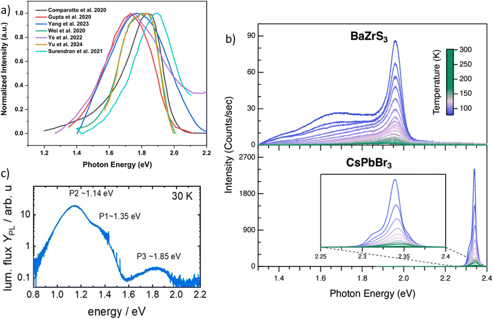 | ||
| Fig. 20 Photoluminescence in BaZrS3. (a) Plot comparing the normalized PL spectra of BaZrS3 synthesized using different methods. (b) Plot showing the temperature-dependent PL spectra of BaZrS3 and CsPbBr3 single crystals. (b) Reproduced with permission.145 Copyright 2024, American Physical Society. (c) Low-temperature PL spectrum of BaZrS3 film grown by H2S sulfurization of Ba–Zr–O film. (c) Reproduced with permission.68 Copyright 2021, American Chemical Society. | ||
In a recent study, Ye et al. compared the photoluminescence spectra of BaZrS3 single crystals grown from BaCl2 flux, BaZrS3 films produced via molecular beam epitaxy, and single crystals of lead halide perovskite CsPbBr3.145 They observed much weaker photoluminescence from BaZrS3 samples than CsPbBr3, with four orders of magnitude higher recombination rate in BaZrS3. This underscores the high concentration of non-radiative recombination centers in the material. Furthermore, the non-radiative recombination in BaZrS3 persisted even at low temperatures, indicating a low thermal activation energy (see Fig. 20b). Márquez et al. also reported two mid-gap defect peaks in their BaZrS3 film, one at 1.14 eV and another at 1.35 eV (shown in Fig. 20c).68 The origin of these defect peaks remains to be determined, but they may be present in other BaZrS3 samples that have not been analyzed at such low energy levels. These peaks closely align with the band positions of the Ruddlesden–Popper (RP) phases of Ba–Zr–S, suggesting the potential presence of nano-domains of RP phases within the bulk BaZrS3.
Pradhan et al. measured the photoluminescence of BaZrS3 samples synthesized by the Agrawal group using various solution chemistries and solid-state powders from BaSx flux, selenium flux, and I2 vapor transport. They observed weak photoluminescence around 1.05–1.15 eV in all samples.123 This weak photoluminescence was attributed to deep defects, such as sulfur interstitials, or the presence of undetected secondary phases in small amounts, such as embedded Ruddlesden–Popper phases. In the absence of a clear understanding, further research is needed to identify origins of this peak, as it may be responsible for quenching the photoluminescence in BaZrS3 samples. Additionally, a recent report clarified that the weak photoluminescence observed by Pradhan et al.117 and Turnley et al.74 was not due to BaZrS3, but rather caused by calcium impurities. The glass substrate that they used contained calcium, which diffused out during the sulfurization step and likely formed CaS:Zr phosphors. These phosphors were amorphous and, therefore, not detectable by X-ray diffraction. The luminescence of these phosphors is very close to the optical bandgap of BaZrS3. These observations underscore the necessity of carefully selecting substrates.123 Similarly, Comparotto et al. did not observe significant photoluminescence from films synthesized in a sulfur atmosphere at temperatures below 600 °C.138 Yang et al.100 and Ravi et al.65 are the only researchers to report notable photoluminescence for BaZrS3 synthesized at temperatures below 600 °C. Notably, Yang et al. found that significant photoluminescence emerged only after water rinsing the synthesized BaZrS3 powder.100
Despite the challenges, the reported minority carrier lifetimes in BaZrS3 are comparable to those of other chalcogenides like Cu(In,Ga)Se2, according to studies by Surendran et al., Wei et al., and Ye et al. (see Fig. 21a and b). Time-resolved photoluminescence (TRPL) data exhibit a biexponential decay, suggesting the coexistence of multiple recombination pathways in the material. This points to the presence of defects, surface recombination, trap states, or different carrier populations. Understanding these processes is crucial for improving the material's optoelectronic properties, especially for applications in photovoltaics and other semiconductor devices. The estimated lifetimes, ranging between 5–50 ns, offer hope, indicating that BaZrS3 may still hold potential.51,72,86 However, the lifetime values with monoexponential decay reported by Yang et al. need to be revisited, as they appear to be outliers (see Fig. 21c).135 Additionally, the solution-processing method by Pradhan et al. achieved only a lifetime of a few hundred picoseconds, highlighting severe recombination centers in those film.117
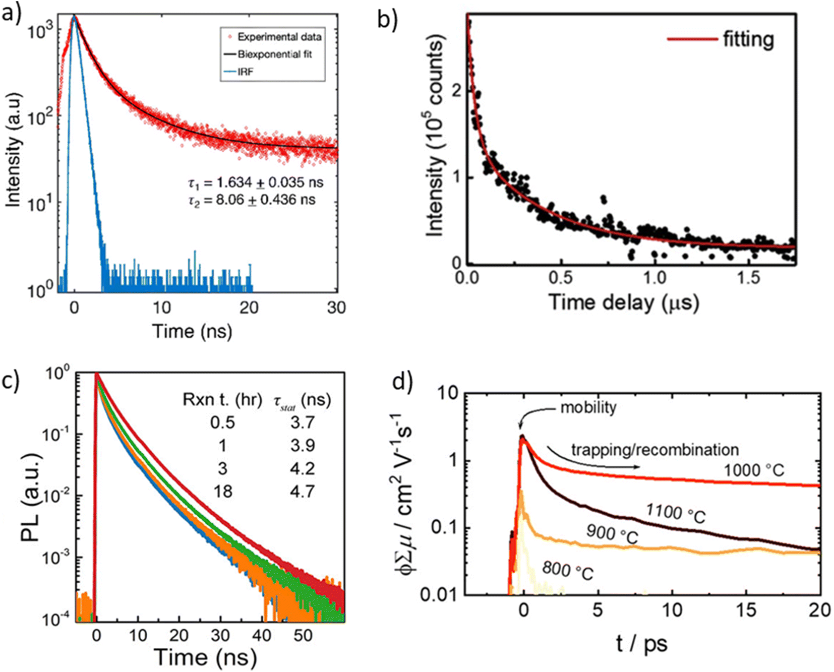 | ||
| Fig. 21 Carrier Lifetime measurements for BaZrS3. (a) TRPL measurement on the epitaxial film of BaZrS3 grown by PLD. (a) Reproduced with permission.72 Copyright 2021, American Chemical Society. (b) Time-resolved PL spectrum of the BaZrS3 thin film sulfurized at 1050 °C for 4 hours, showing time constants τ1 and τ2 as 40 ns and 400 ns, respectively, from the bi-exponential fitting. (b) Reproduced with permission.86 Copyright 2020, Elsevier. (c) TRPL spectra of BaZrS3 nanoparticles grown by Yang et al.135 (c) Reproduced with permission.135 Copyright 2022, American Chemical Society. (d) Transient photoconductivity measurements on BaZrS3 films grown by H2S sulfurization of Ba–Zr–O films. (d) Reproduced with permission.68 Copyright 2021, American Chemical Society. | ||
The transient photoconductivity measurements on BaZrS3 film synthesized by Márquez et al. at 1000 °C also showed a fast initial decay followed by a longer time constant of around 30 ps, which could possibly be attributed to the trapping of carriers into localized states or the very fast recombination of charge carriers (shown in Fig. 21d).68 Zhao et al. also observed a similar pattern in the transient photocurrent measurement of BaZrS3 single crystal, where the photoexcited carriers showed a fast initial decay followed by a slow decay.146
The overall poor photoluminescence in BaZrS3 necessitates a thorough investigation into the presence of deep defects, which may arise from unoptimized synthesis conditions rather than being intrinsic to the material. Improvements in defect control during synthesis and processing are critical for BaZrS3's potential in optoelectronic applications and represent a significant challenge for its adoption.
3.4. Optical bandgap
The Tauc plot is a widely used method for estimating the optical bandgap of semiconductors and insulators. It is based on the Tauc equation, which relates the absorption coefficient of a material to photon energy and the type of electronic transition. However, the bandgap determination from the Tauc plot may not be fully accurate due to the simplifications inherent in the approach, which requires an assumption about the type of electronic transition (e.g., direct allowed, direct forbidden, indirect allowed, or indirect forbidden). The estimated bandgap may be imprecise if the assumed transition type is incorrect. On these lines, Nishigaki et al. reported that the lowest transition (V1 → C1) is forbidden in BaZrS3 and the next lowest allowed transition (V2 → C2) is 0.1 eV higher than the bandgap. This might lead to errors in the bandgap estimation from Tauc plot which has also been reflected in a wide range of bandgap reported for BaZrS3 in the literature 1.7–1.95 eV.67Additionally, the extrapolation of the linear portion of the Tauc plot can be subjective. Determining the exact onset of absorption can also be challenging, particularly in materials with tails in their absorption spectra due to defects, disorder, or other non-idealities. This can lead to an overestimation or underestimation of the bandgap. The assumption of ideal optical absorption processes, such as neglecting excitonic effects, may not always hold and could also lead to errors.
Given these limitations, the Tauc plot is not solely relied upon in the literature and is often complemented with other techniques like photoluminescence, which measures band-to-band emission and is generally considered more reliable. However, as discussed in detail in the previous section, photoluminescence peaks vary significantly across samples and methods in the BaZrS3 literature, leading to a need for a clearer consensus on the actual bandgap. It is believed to be around 1.8 eV, generally within the 1.7–1.9 eV range.40,48,62,65,86,93,140,147
Surprisingly, the absorption spectra of BaZrS3 nanoparticles synthesized by Zilevu et al.135,136 and Yang et al.135 indicate a bandgap greater than 2 eV. Consequently, these data warrant further investigation. The trends in photoluminescence peaks typically correlate with bandgap estimations from the Tauc plot in the BaZrS3 literature. Fig. 22a and b presents the Tauc plot for various synthesis methods and displays a wide range of bandgaps. These variations emphasize the need for streamlined synthesis processes and optimized conditions to achieve consistent results. The bandgap has been estimated to be approximately 2.1 eV for BaHfS3 using Tauc plot analysis.67,85,105
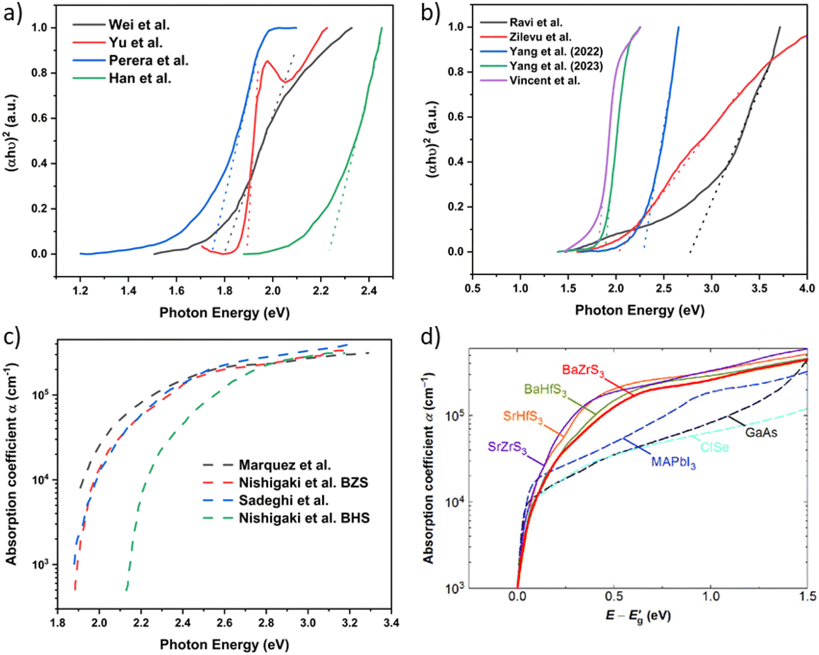 | ||
| Fig. 22 Bandgap and absorption measurements for BaZrS3. (a) Tauc plot showing the estimated bandgap for BaZrS3 grown via different methods at temperatures (a) exceeding 600 °C, (b) below 600 °C. (c) Absorption coefficient measurements of BaZrS3 and BaHfS3 grown via different methods. (d) Comparison of the absorption coefficients of chalcogenide perovskites with other notable semiconductors. (d) Reproduced with permission.67 Copyright 2020, Wiley. | ||
3.5. Absorption coefficient
A high absorption coefficient is desirable for solar cell absorbers as it minimizes the required thickness to absorb nearly all incoming light, thereby reducing material consumption. A thinner film also decreases the series resistance in the solar cell and can accommodate lower carrier lifetimes and mobility. Density Functional Theory (DFT) studies have shown that chalcogenide perovskites, including BaZrS3, possess a high absorption coefficient exceeding 105 cm−1 within 0.3–0.5 eV above the onset of absorption.67,143 This absorption coefficient is significantly higher than that of other commercialized and emerging chalcogenides such as Cu(In,Ga)Se2 and Cu2ZnSnSe4, and is comparable to or slightly better than lead halide perovskites.148,149 This high absorption is attributed to the high density of states in the valence and conduction bands of BaZrS3 and other chalcogenide perovskites, where sulfur 3p orbitals constitute the valence band edges and transition metal d orbitals constitute the conduction band edges. This high absorption has also been experimentally verified (see Fig. 22c).67,68,89,140 Furthermore, the light absorption in these materials has been shown to be sharp, resulting in low Urbach energies (22–34 meV), which can help mitigate open-circuit voltage losses in photovoltaic (PV) devices.67 However, Márquez et al. reported that the absorption coefficient does not conform well to the parabolic band assumption, and the relation α ∝ (E − Eg)0.5 does not hold.68 Nishigaki et al. explained this discrepancy based on the forbidden lowest energy transition and the next-lowest energy transition being 0.1 eV above the bandgap.67 On one hand, this high light absorption coefficient indicates that an absorber film only 100–200 nm thick is required to absorb all incoming light completely. On the other hand, synthesizing such thin films remains challenging for BaZrS3. Nonetheless, Nishigaki et al. compared the absorption spectra of chalcogenide perovskites, including BaZrS3 and BaHfS3, with MAPbI3 and other notable inorganic semiconductors, finding that the former exhibited markedly superior performance (see Fig. 22d).67 The synthesis conditions notably influence the absorption coefficient of BaZrS3, as Márquez et al. observed that it significantly red-shifts and increases in magnitude with enhanced crystallinity and sulfur content.68 In a different study, Xu et al. sulfurized BaZrO3 powder using CS2 to synthesize BaZrS3 and observed that the absorbance decreased with an increasing amount of sulfur in the mixture. Conversely, post-annealing of fully converted BaZrS3 in air below 500 °C increased the absorbance, suggesting that oxygen impurities in BaZrS3 might actually be beneficial.140 Therefore, although the material exhibits promising light absorption properties, synthesis-related challenges need to be overcome to fully exploit this potential.3.6. Carrier properties
The literature contains numerous examples of solar absorbers that, despite having promising optical bandgaps, lack essential carrier properties such as low effective carrier masses, high carrier mobility, low resistivity, and optimal carrier concentration.150–152 These properties are crucial for ensuring the unrestricted flow of carriers by minimizing traps throughout the material while maintaining a sufficiently high carrier concentration to form a p–n/p–i–n junction for the effective separation of light-generated charge carriers. Although BaZrS3 is still in its early stages of development, there has been inconsistency in the reported carrier properties. Wei et al. confirmed n-type conductivity in BaZrS3 films synthesized by CS2 sulfurization of pulsed laser deposition (PLD) deposited BaZrO3 films. They observed n-type conductivity in all samples sulfurized at temperatures between 900–1050 °C, attributing this to sulfur vacancies. For sulfur vacancies to contribute electrons to the conduction band and result in n-type conductivity, these vacancies must be shallow defects with low formation energy.86 Wu et al. and Yuan et al., through computational defect chemistry studies, confirmed that sulfur vacancies act as shallow donor defects in BaZrS3, suggesting that the sulfur vacancies formed at high sulfurization temperatures are likely responsible for the observed n-type conductivity.122,142 Interestingly, Wei et al. reported high doping density in their BaZrS3 films, with carrier concentrations on the order of 1019–1020 cm−3.86 This implies that approximately one in every 100–1000 sulfur atoms is missing, contributing to the remarkably high doping density. Additionally, finding a compatible p-type layer for n-type BaZrS3 with such high carrier density poses a challenge, limiting its integration into conventional solar cell architectures. Nonetheless, there may be ways to reduce the n-type carrier density, such as external p-type doping to compensate for the high n-type doping. The high carrier density also results in a moderately high conductivity of 3.52–588 S cm−1. Wei et al. also reported a respectable carrier mobility of 13.7 cm2 V−1 s−1 for a film synthesized at 1050 °C and noted that the carrier mobility increased with sulfurization temperature (see Fig. 23a–c). Based on conductivity measurements as a function of temperature, they proposed the Efros-Shklovskii variable range hopping model to describe charge carrier transport in BaZrS3 films and estimated an activation energy of 1.7 meV. This energy was attributed to the ionization energy of sulfur vacancies. Their analysis indicated that sulfur vacancies can be easily ionized at room temperature, leading to a high electron concentration.86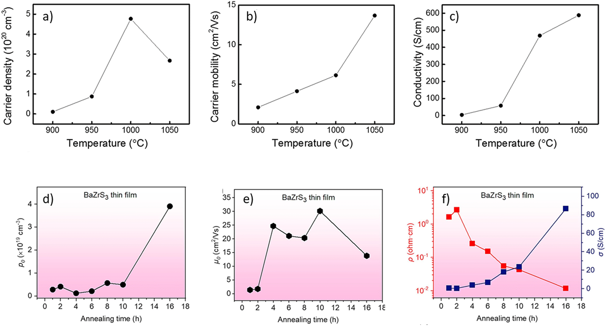 | ||
| Fig. 23 Charge carrier properties of BaZrS3. (a)–(c) Plots showing the variation in carrier density, carrier mobility, and conductivity with growth temperature for BaZrS3 film synthesized by CS2 sulfurization of BaZrO3 film. (a)–(c) Reproduced with permission.86 Copyright 2020, Elsevier. (d)–(f) Plots showing the variation in carrier density, mobility, and resistivity/conductivity with annealing temperature for BaZrS3 film grown by magnetron sputtering from a BaZrS3 target. (d)–(f) Reproduced with permission.48 Copyright 2023, Elsevier. | ||
Differing from Wei et al., Yu et al. also reported ambipolar conductivity in BaZrS3 films synthesized by CS2 sulfurization of pulsed laser deposition (PLD)-deposited amorphous films at 500 °C. They argued that a lower concentration of sulfur vacancies would result from annealing at a lower temperature. They confirmed n-type conductivity with a significantly lower electron concentration of 4.4 × 1010 cm−3 when operating the constructed field-effect transistor with positive gate voltage. A similar but lower current magnitude was measured with negative gate voltage, indicating ambipolar characteristics. They further estimated the electron and hole mobilities to be approximately 16.8 and 2.6 cm2 V−1 s−1, respectively.93 The smaller crystallite size resulting from the low-temperature sulfurization step may have increased carrier scattering, reducing carrier mobility. Ravi et al. also reported ambipolar electron-dominated conductivity for the colloidal BaZrS3 nanocrystals.65
Recently, Aggarwal et al. demonstrated insulating behavior in BaZrS3 films synthesized by sputtering Ba and Zr onto a substrate, followed by sulfurization in a sulfur atmosphere.153 However, these films exhibited dominant n-type conductivity when annealed under vacuum at temperatures between 500 °C and 600 °C. This was attributed to sulfur loss from the film, leading to shallow sulfur vacancy defects. The sulfur vacancies contribute electrons to the conduction band, causing the carrier concentration to increase beyond 1020 cm−3, which is sufficiently high for delocalizing shallow defect levels and overlapping with the conduction band edge. While the carrier concentration varied with increasing annealing temperature and time, the carrier mobility remained stagnant around 1 cm2 V−1 s−1. The authors attributed this to grain boundary scattering or phonon scattering, possibly unrelated to ionized impurity scattering. However, the carrier concentration saturated after reaching 1022 cm−3. Temperature-dependent Hall effect measurements revealed a low activation energy of 8 meV, indicating a shallow donor defect. Similarly, Mukherjee et al. reported n-type conductivity for BaZrS3 films achieved by co-sputtering Ba–Zr–S and annealing the film at 950 °C, as evidenced through hard X-ray photoelectron spectroscopy.141 Additionally, Yang et al. reported n-type conductivity for BaZrS3 bulks with a carrier concentration of 1.02 × 1019 cm−3 and a high mobility of 354 cm2 V−1 s−1.66
Many emerging chalcogenide absorbers exhibit p-type conductivity and have found suitable n-type junction partners. Therefore, a p-type BaZrS3 film might easily find an n-type junction partner. In this context, Han et al. reported BaZrS3 films with p-type conductivity.48 They synthesized BaZrS3 films at 1000 °C via CS2 sulfurization of amorphous PLD-deposited Ba–Zr–S films and suspected Ba-loss during the growth, resulting in Ba-deficient films. Since barium vacancies are expected to act as shallow acceptor defects, their films demonstrated p-type conductivity, which is rarely reported for BaZrS3. They further noted that the film's conductivity improved with extended annealing time, which was attributed to increased carrier concentration and hole mobility. The mobility enhancement was suggested to result from reduced defect scattering due to the improved quality of the film after prolonged annealing. Additionally, longer annealing times likely led to increased barium loss, thereby increasing the hole concentration after annealing for more than 10 h. While the highest carrier concentration of 1019 cm−3 was achieved after annealing for 16 h, mobility was compromised. An annealing duration of 4–10 h was found to be optimal, yielding a mobility of 30 cm2 V−1 s−1 and a carrier concentration of 1018 cm−3 (see Fig. 23d–f). Temperature-dependent Hall effect measurements indicated an Efros-Shklovskii variable range hopping relationship between conductivity and temperature, from which an activation energy of 26.22 meV was estimated. This activation energy can be roughly interpreted as the ionization energy between the acceptor levels and the valence band edge, suggesting that the acceptor levels in BaZrS3 are shallow.
Instead of performing hall effect measurements, Ravichandran and his collaborators estimated p-type conductivity for the BaCl2 flux-grown BaZrS3 single crystal by measuring the surface photovoltage using the Kelvin probe microscopy.146 They estimated a positive photovoltage for all the wavelengths tested, which indicates either a p-type conductivity or hole-transport dominated ambipolar nature of BaZrS3, which could have been induced by the barium or zirconium vacancies during the growth. This is in contrast to the frequently reported n-type conductivity for BaZrS3. Márquez et al. also estimated the combined mobilities of photoexcited electrons and holes from the photoconductivity decay measurements for samples sulfurized under H2S at 1100 °C; a combined mobility of approximately 2 cm2 V−1 s−1 was observed.68
The literature on the carrier properties of BaZrS3 is limited, with most studies focusing on films synthesized at high annealing temperatures. These films often suffer from barium or sulfur loss, resulting in high concentrations of holes or electrons due to shallow barium and sulfur vacancies. Therefore, a systematic study of the effects of different synthesis conditions, such as annealing temperature, time, and sulfur pressure, on the carrier properties is necessary. Additionally, it would be valuable to investigate the carrier properties of BaZrS3 films produced by recently reported low-temperature solution-processing methods. However, film discontinuity in such methods may limit the measurements. The intrinsic nature of BaZrS3 at low synthesis temperatures might also result in extremely high resistivity in the films, making measurement challenging. Nonetheless, controlling the carrier concentration in BaZrS3 through self-doping or extrinsic doping, along with achieving low effective carrier masses and high mobility, is crucial for the material's utility in electronic devices.
3.7. Polymorphism
Polymorphism refers to the ability of a material to adopt different crystal structures while maintaining the same chemical composition. This phenomenon is often influenced by factors such as pressure, temperature, the type of precursors, and other synthesis conditions. Polymorphism is significant because it can drastically alter a material's optical, electronic, and mechanical properties, enabling its use in diverse applications. For instance, WSe2 exhibits polymorphism, where the 2H phase is semiconducting while the 1T phase is metallic.154BaZrS3, a chalcogenide perovskite, exhibits an orthorhombic Pnma ground state that has been experimentally verified.28 However, Kayastha et al. used molecular simulations to demonstrate that, at ambient pressure (0 Pa), BaZrS3 can exist in three distinct polymorphs.155 They found that the orthorhombic Pnma phase remains stable up to 610 K, beyond which it transitions to a tetragonal I4/mcm phase. At temperatures above 880 K, it converts to a cubic Pm![[3 with combining macron]](https://www.rsc.org/images/entities/char_0033_0304.gif) m phase, which is commonly observed in halide and oxide perovskites but had not previously been reported for BaZrS3. Furthermore, Kayastha et al. conducted calculations across varying pressures and temperatures, constructing a comprehensive phase diagram for BaZrS3.
m phase, which is commonly observed in halide and oxide perovskites but had not previously been reported for BaZrS3. Furthermore, Kayastha et al. conducted calculations across varying pressures and temperatures, constructing a comprehensive phase diagram for BaZrS3.
Recently, Jaiswal et al. experimentally validated polymorphism in BaZrS3 by heat-treating BaZrS3 powder in air at various temperatures.156 Using in situ high-temperature X-ray diffraction, Raman spectroscopy, and bandgap measurements, they characterized the structural phases and optical properties. Their observations diverged slightly from those of Kayastha et al.155 Jaiswal et al. reported that orthorhombic Pnma BaZrS3 transitions to a Cmcm phase at approximately 400 °C, which subsequently transforms into the tetragonal I4/mcm phase above 500 °C.156 However, since the heating was done in air, due to oxidation, the BaZrS3 powder began degrading above 500 °C and decomposed completely around 700 °C. No additional phases were observed between 500 °C and 700 °C.
In situ bandgap measurements revealed that within a single phase, the bandgap decreased with increasing temperature. A sharp discontinuity in the bandgap was observed during phase transitions, with the Pnma phase exhibiting the highest bandgap and the I4/mcm phase the lowest. Notably, upon cooling, the orthorhombic Pnma phase was restored. These findings on BaZrS3 polymorphism are intriguing, as the distinct phases may exhibit other divergent properties. However, isolating these phases at room temperature remains a significant challenge.
3.8. Alloying
Li et al., using first-principles and molecular dynamics simulations, suggested that Ti alloying enhances phonon–electron coupling in BaZrS3, leading to localized polarons that affect carrier mobility. This could potentially result in increased electron–hole recombination and reduced photogenerated carrier lifetime due to alloying with Ti.157 Nishigaki et al. attempted Ti alloying in BaZrS3 by annealing ground binary sulfide powders. They reported a bandgap reduction for 5% Ti alloying but observed phase segregation at 10% Ti alloying. Additionally, they found that alloying broadened the band-edge absorption, leading to high Urbach energy while maintaining a high absorption coefficient (see Fig. 24a). They attributed the tail absorption to atom clustering due to limited Ti–Zr solubility or unoptimized synthesis conditions.67
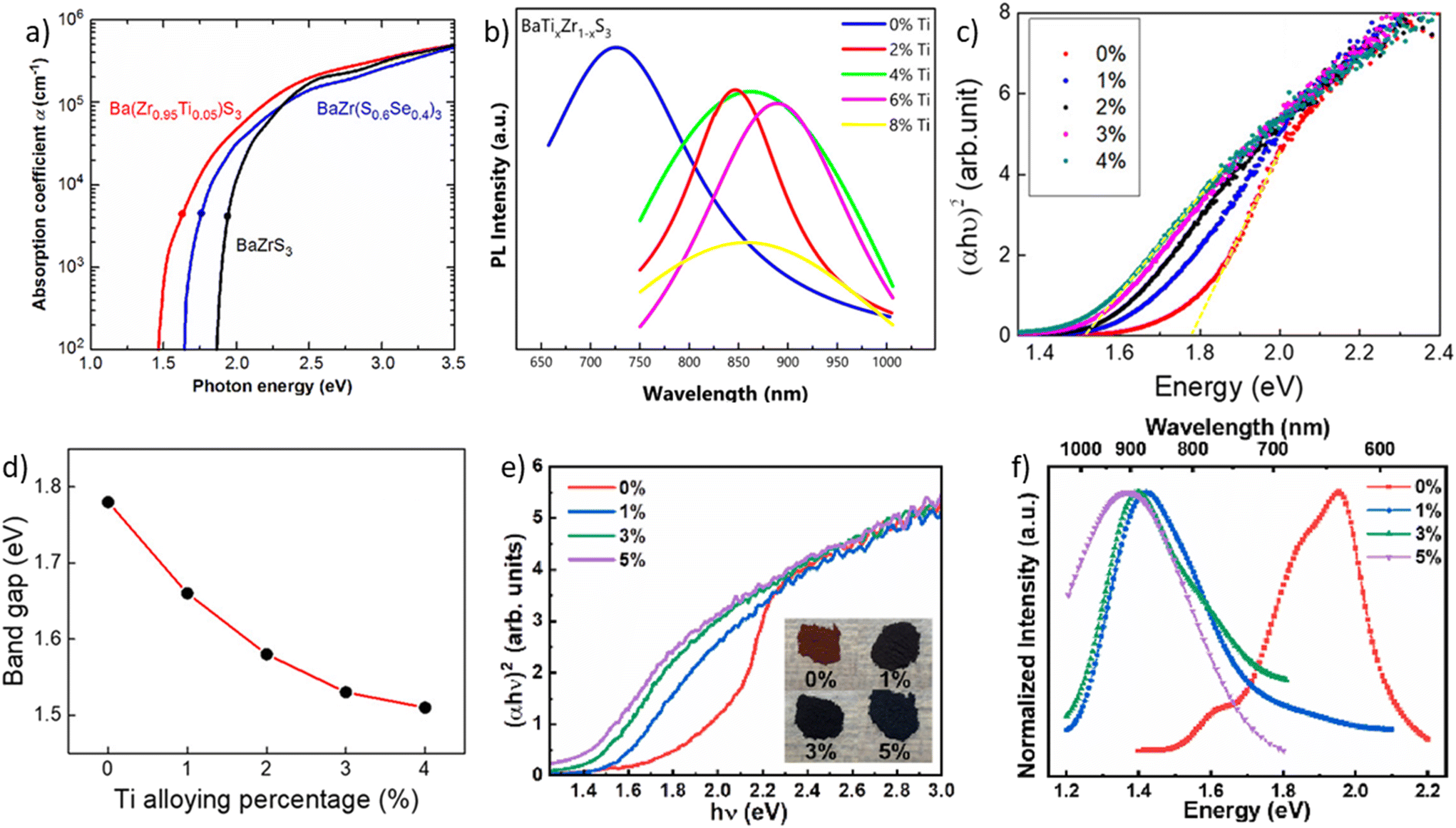 | ||
| Fig. 24 Ti alloying in BaZrS3 and BaHfS3. (a) Comparison of the absorption coefficients for BaZrS3 and Ba(Zr0.95Ti0.05)S3. (a) Reproduced with permission.67 Copyright 2020, Wiley. (b) Comparison of the PL spectra for BaZrS3 and Ti-alloyed BaZrS3. (b) Reproduced with permission.96 Copyright 2021, American Chemical Society. (c) and (d) Variation in the bandgap with Ti-alloying in BaZrS3. (c) and (d) Reproduced with permission.57 Copyright 2020, American Chemical Society. (e) and (f) Variation in the bandgap and PL spectra with Ti-alloying in BaHfS3. (e) and (f) Reproduced with permission.85 Copyright 2024, Elsevier. | ||
Koratkar group synthesized thin films of Ba(Zr,Ti)S3 and observed a similar monotonic reduction in bandgap with increasing Ti percentage.96 However, their alloyed films suffered from significant photoluminescence quenching and peak broadening compared to the parent BaZrS3, indicating defect formation from alloying. They also observed phase segregation beyond 6% alloying, with no further bandgap reduction (shown in Fig. 24b). Zeng group also attempted the powder synthesis of Ba(Zr,Ti)S3 and reported a monotonic decrease in bandgap with increasing Ti content, reaching 1.51 eV with only 4% Ti alloying.57 Higher alloying concentrations destabilized the perovskite phase (see Fig. 24c and d). Similar to Nishigaki et al., they observed an absorption tail in the 4% alloyed sample, attributing it to secondary phases.
Han et al. deposited thin films of Ba(Zr,Ti)S3 by co-sputtering from BaZrS3 and BaTiS3 targets, observing phase separation beyond 5% Ti alloying.48 They reported a bandgap reduction to 1.5 eV with 4% Ti alloying. Electrical characterizations of their unoptimized film with pinholes showed high sheet resistance compared to pure BaZrS3 films. Additionally, they reported p-type conductivity for their 4% Ti alloyed film, with a hole concentration of 6 × 1018 cm−3 and a carrier mobility of 6 cm2 V−1 s−1, which was significantly decreased compared to BaZrS3, likely due to increased scattering effects.
In a recent study, Creutz group explored Ti alloying in BaZrS3 nanoparticles, reporting alloying levels up to 11%.158 While the behavior of materials at the nanoscale can differ and allow for greater alloying, the synthesized BaZrS3 nanoparticles and their alloys did not posses the correct phase in this study. Consequently, any higher percentage of Ti alloying in these nanoparticles require further exploration. Nonetheless, this work marks a significant step forward in attempting alloying at the nanoscale.
Similar to Ti alloying in BaZrS3, Ti alloying in BaHfS3 is also a promising approach to reduce its bandgap and enhance its suitability for photovoltaic applications. Kong et al. conducted powder synthesis of Ti alloying in BaHfS3 and observed a reduction in bandgap with no secondary phases up to 5% Ti alloying. UV-Vis measurements revealed that a 5% Ti alloying resulted in a bandgap of 1.4 eV for Ba(Hf,Ti)S3 (see Fig. 24e). A similar shift in the photoluminescence peak was also observed for Ti alloying in BaHfS3 (shown in Fig. 24f).85
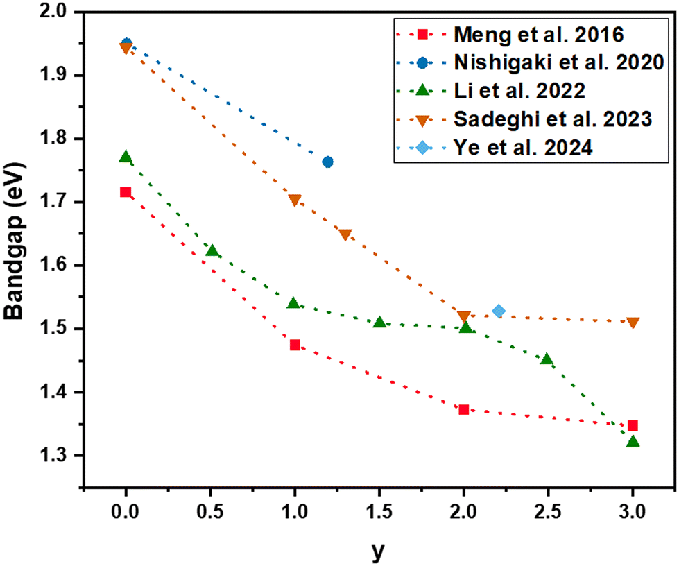 | ||
| Fig. 25 Plot showing the reductions in bandgap for selenium-alloyed BaZr(S3−y,Sey)3. | ||
However, few experimental reports have attempted selenium alloying in BaZrS3. Nishigaki et al. conducted powder-based synthesis of BaZr(S,Se)3 by mixing BaS, ZrS2, and ZrSe2 powders and annealing them at temperatures exceeding 1100 °C. They observed a monotonic decrease in the bandgap up to 40% Se alloying, beyond which phase segregation occurred. The bandgap decreased by approximately 0.25 eV with 40% Se alloying, with light absorption shifting towards lower energies. Similar to Ti alloying, they noted broadening of the absorption spectrum with Se alloying, resulting in an Urbach energy of 50–70 meV, likely due to increased scattering by atomic clusters or unoptimized synthesis. Additionally, they observed impurities of the Ruddlesden–Popper Ba3Zr2S7 phase in their 40% selenium alloyed sample, complicating the accurate estimation of the alloyed content and the observed properties.67
While thermal equilibrium growth conditions have resulted in a relatively low alloying limit for selenium in BaZrS3, non-thermal equilibrium growth techniques can potentially overcome this limitation and stabilize higher selenium content in BaZrS3. Jaramillo group demonstrated this by growing Ba–Zr–S–Se films using gas source molecular beam epitaxy with H2S gas as the sulfur source, stabilizing the full range of compositions BaZrS(3−x)Sex in the perovskite structure, where 0 < x < 3.90 As expected, the bandgap decreased with increasing Se content, with phase-pure BaZrS3 having a bandgap of around 1.9 eV and BaZrSe3 around 1.5 eV. They constructed photodetectors using these films by depositing Ti/Au electrodes on the film's surface and measured the responsivity of the photodetectors. Interestingly, they noted that the responsivity decreased monotonically by several orders of magnitude with increasing selenium content. This significant reduction in responsivity severely limits the utilization of selenium doping in BaZrS3 and could be due to various factors, such as increased bulk or surface defects, which may depend on processing conditions and composition and thus require detailed study.
In other notable work, the Jaramillo group demonstrated the synthesis of BaZr(S,Se)3 films through anion exchange of sulfur with selenium in BaZrS3 films in an H2Se atmosphere at 800 °C without disturbing the microstructure of the original BaZrS3 films.61 This method does not require the films to be epitaxially grown, and the full range of compositions was achieved for both epitaxial and polycrystalline thin films of BaZrS3. Importantly, they noted that photoresponsivity was orders of magnitude higher for selenium alloyed films grown by the anion exchange method compared to direct growth, possibly due to the reduction of extended defects.
Romagnoli et al. synthesized powders of BaZrS3, BaHfS3, and their mixtures by annealing BaS, Zr, Hf, and sulfur powders in an ampule at temperatures below 550 °C.147 As anticipated, they observed homogeneous alloying across the entire composition range. The researchers noted a gradual decrease in lattice parameters and an increase in the bandgap as the Hf content in the mixture increased.
Chami et al., through first-principle calculations, demonstrated that substituting Zr with Sn is feasible up to 25%, resulting in a monotonic decrease in the bandgap with increasing Sn content.60 They predicted a reduction in the bandgap to below 1 eV with 25% Sn alloying and noted a high absorption coefficient for the alloyed sample, accompanied by a red shift in the absorption onset. While these calculations indicate a promising reduction in the bandgap and enhanced optoelectronic properties, achieving 25% Sn alloying in polycrystalline samples might be difficult due to the different structures of the terminal ternaries.
Nonetheless, Sharma et al. conducted experimental synthesis to verify their findings and observed a significant red shift in the photoluminescence peak with Ca alloying, with the bandgap reduction stabilizing after 2% alloying. While there exists a photoluminescence peak at 985 nm, a broad tailing towards lower wavelengths was also observed, indicating the potential presence of secondary phases. Compared to Ti alloying, they suggested that Ca alloying resulted in less quenching of photoluminescence, possibly due to fewer defects.
While Ca alloying appears to be a promising method to reduce the bandgap of BaZrS3, a more comprehensive study is needed to investigate the solubility limit of Ca in BaZrS3, the defects formed, the band tailing towards higher energies, and the impact on carrier transport. This would be necessary to confirm its reliability as a method for bandgap reduction compared to Ti or Se alloying.
3.9. Effect of pressure
High pressure can significantly influence the electronic and mechanical properties of a material. It can lead to modifications in the band structure as the atomic distances change, affecting the bandgap, conductivity, and other electronic properties. Mechanically, high pressure typically increases stiffness and hardness and can induce phase transitions that fundamentally alter the material's structure and properties. Rong et al. conducted ab initio DFT calculations to determine the effect of pressures up to 20 GPa on the structure of BaZrS3.162 They observed that the ductility of BaZrS3 increased with pressure, as did the dielectric constant. Additionally, all the peaks of the optical constants shifted to lower energies, i.e., they exhibited red shifts. Gross et al. experimentally confirmed a red shift in the absorption edge with increasing pressure, noting a decrease of approximately 0.015 eV GPa−1. They also did not observe any structural changes in BaZrS3 up to 8.9 GPa.833.10. Properties of BaTiS3
Unlike BaZrS3 and BaHfS3, BaTiS3 is important for its quasi-1D structure, which unlocks a range of interesting properties. Notably, it exhibits giant optical anisotropy and electronic phase transitions, which enable functionalities such as polarization detection and resistive switching.131,132 BaTiS3 demonstrates optical anisotropy at mid-wave and long-wave infrared energies, making it an excellent candidate for polarization-selective infrared optics (shown in Fig. 26a).163 | ||
| Fig. 26 Photoelectric performance of BaTiS3 photodetectors and the electronic configuration. (a) Transmission spectrum of the atmosphere in the mid-IR range, showing the band gaps of various two-dimensional (graphene, BP, b-AsP, and Te) and quasi one-dimensional materials (BaTiS3). (a) Reproduced with permission.163 Copyright 2021, Springer Nature. Defect characterization and photoelectric performance of BaTiS3 single crystal photodetectors. (b) Configuration of the BaTiS3 photoconductive detector under near-infrared light irradiation. (c) Temperature-dependent conductivity and corresponding Arrhenius fitting of pristine and sulfurized BaTiS3 single crystals from 80 to 320 K. (d) Linear and quadratic fittings according to the SCLC model. (e) and (f) Comparison of the temporal photocurrent response performance for pristine and sulfurized BaTiS3 photodetectors at room temperature (RT) and 80 K, @1 V, 780 nm illumination with a power density of 12.8 mW cm−2. (g) Time-resolved photoresponse speed of the BaTiS3 photodetector under 780 nm illumination, @1 V, 80 K. (h) Light intensity-dependent responsivity and detectivity of the BaTiS3 photodetector under 780 nm illumination, @1 V, 80 K. (i) Tauc plot from the optical absorption spectrum of BaTiS3 films showing an Eg ≈ 0.8 eV. (j) UPS spectrum (left) and the valence band spectrum (right) of BaTiS3 with He 1 excitation. (b)–(j) Reproduced with permission.165 Copyright 2020, Springer Nature. | ||
While reports exist on nanocrystals and quasi-epitaxial thin films of BaTiS3, emerging studies highlight the large single crystals synthesized either through chemical vapor transport (CVT) or metal salt fluxes such as BaI2, BaCl2, or KI.91,124,125 Interestingly, single crystals obtained from KI flux have been significantly larger in volume compared to those synthesized from chemical vapor transport or barium salt fluxes.132
Chen et al. achieved a high birefringence of 0.8 in the mid-infrared region for wavelengths of 4 μm and above in their KI flux-grown (001) oriented BaTiS3 crystals and discovered a high dichroic window from 1 to 4 μm.132 Previously, Niu et al. measured a high birefringence of 0.76 in their CVT-grown single crystals and observed two distinct absorption edges at 0.28 eV and 0.78 eV, resulting in a large dichroic window.164 Yang et al. studied the photoelectric properties of BaTiS3 and fabricated a polarized photodetector using an Ag/BaTiS3/Ag architecture, which showed a broad wavelength detection range from visible light to 1550 nm and a high responsivity of 1.22 A W−1 and detectivity of 3.8 × 10¹⁰ Jones under 780 nm illumination. The photodetector device characteristics are shown in Fig. 26b–h. Yang et al. also reported excellent transport properties for CVT-grown and sulfur-treated BaTiS3 crystals with mobility around 300 cm2 V−1 s−1 along the c-axis and n-type conductivity. These exciting properties suggest that BaTiS3 could have applications in optical communication and integrated polarization sensors, among other fields.131
The measured bandgap, band positions and other properties of BaTiS3 are listed in Table 2 and Fig. 26i–j. The low thermal conductivity and structural anisotropy of BaTiS3 could also make it favorable for thermoelectric applications. Sun et al. identified glass-like ultralow thermal conductivity in pristine, high-quality crystals of BaTiS3, attributed to sub-THz frequency atomic tunneling states.165 Using first-principles calculations, Paudel et al. estimated a maximum power factor of 928 μW K−2 and a thermoelectric figure of merit (ZT) of 0.48 for electron-doped BaTiS3, and a power factor of 74 μW K−2 and ZT of 0.17 for a hole-doped sample at room temperature. The power factor and ZT increase with temperature, reaching a ZT of 0.77 for electron-doped BaTiS3 at 800K.30 These impressive values underscore the thermoelectric potential of BaTiS3.
| Property | Value |
|---|---|
| Thermal conductivity (W m−1 K−1) | 0.39 (ref. 165) |
| zT | 0.48 (e− doped sample), 0.17 (h+ doped sample) (ref. 30) |
| Bandgap | 0.85 (ref. 131), 0.5 (ref. 30) |
| Conductivity | n-Type (ref. 131) |
| Fermi level (eV) | 4.92 (ref. 131) |
| Deep defect activation energy (eV) | ∼0.44 (ref. 131) |
| Shallow defect activation energy (eV) | ∼0.11 (ref. 131) |
| Dielectric constant | 2152 (ref. 131) |
| Crystal mobility (cm2 V−1 s−1) | 322 (ref. 131) |
| Powder carrier concentration (cm−3) | 3.6 × 10¹⁶ (ref. 131) |
| Responsivity (@780 nm, 1 V, 80 K) | 1.22 A W−1 (ref. 131) |
| Absorption edges | (0.35 eV, 0.77 eV) (ref. 132), (0.28 eV, 0.78 eV) (ref. 164) |
| Birefringence | 0.8 (ref. 132), 0.76 (ref. 164) |
| Dichroic window | 1 to 4 μm (ref. 132) |
4. Working applications of BaZrS3
4.1. Photo detectors
A photodetector can be one of the simplest devices to test the functionality of a semiconductor material, and has thus been frequently fabricated in BaZrS3 research. Koratkar group deposited gold contacts on their CS2-sulfurized BaZrS3 film to create the device and fabricated a similar device with MAPbI3 for comparison (shown in Fig. 27a).62 They observed a high dark current in the BaZrS3 film, which they attributed to a high number of sulfur vacancies formed due to annealing at high temperatures. Consequently, the photocurrent was estimated by subtracting the dark current from the current under illumination. Interestingly, the measured responsivity value of 46.5 mA W−1 at 5 V for the BaZrS3 photodetector is comparable to the reported values for lead halide perovskites and the MAPbI3 device they fabricated. While the responsivity of BaZrS3 decreased by 40% after 4 weeks in ambient conditions, the responsivity of MAPbI3 reduced by 95% in just 4 days, and the film decomposed into PbI2 (see Fig. 27b).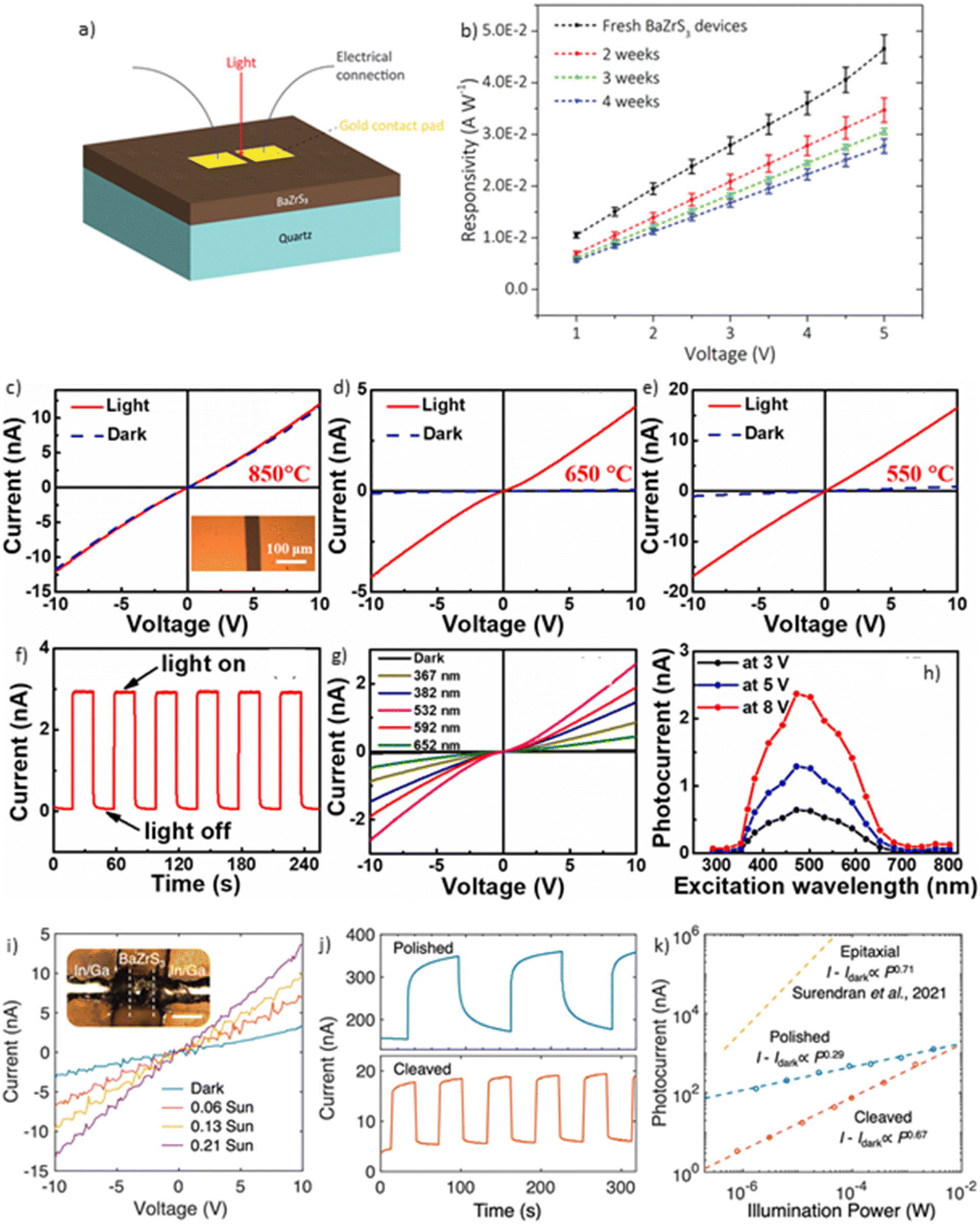 | ||
| Fig. 27 Photoelectric performance of BaZrS3 photodetectors. (a) and (b) Photodetector design and photoresponsivity measurements as a function of applied voltage for BaZrS3 film grown via CS2 sulfurization of solution-deposited BaZrO3 film. (a) and (b) Reproduced with permission.62 Copyright 2020, Wiley. (c)–(e) Current–voltage measurements under dark and illumination conditions for BaZrS3 films annealed at different temperatures during growth. (f) Current vs. time for the device using the film annealed at 650 °C, with a periodically switched light source (532 nm) at a fixed bias of 8 V. (g) I–V curves measured at different excitation wavelengths for the device using the film synthesized at 650 °C. (h) Wavelength-dependent photocurrent at bias voltages of 3, 5, and 8 V extracted from (g). (c)–(h) Reproduced with permission.93 Copyright 2021, Elsevier. (i) Photocurrent vs. voltage for different illuminations. (j) Transient photocurrent measurements. (k) Photocurrent as a function of illumination power for BaZrS3 single crystal. (i)–(k) Reproduced with permission.146 Copyright 2024, American Chemical Society. | ||
Unlike the Koratkar group, Zeng group deposited BaZrO3 films using pulsed laser deposition and sulfurized them in a flowing CS2 environment at 1050 °C.86 They also observed a high dark current, which was very similar to the current under light, thereby affecting the proper measurement of photoresponse. It was argued that the high annealing time at such temperatures led to a large number of sulfur vacancies, resulting in high carrier concentration and affecting the photoresponse measurements. However, reducing the annealing time significantly increased the sample resistivity and decreased the dark current by three orders of magnitude, further confirming that sulfur vacancies were inflating the carrier concentration. Consequently, a decent photoresponse was obtained.
Zeng group also fabricated photodetectors using BaZrS3 films synthesized by CS2 sulfurization of PLD-deposited amorphous Ba–Zr–S films.93 They produced devices for films sulfurized at 550 °C, 650 °C, and 850 °C. Similar to the earlier findings, they reported a high dark current for the film sulfurized at 850 °C, likely due to sulfur vacancies that resulted in a high intrinsic carrier concentration, overshadowing any photoresponse. However, much lower dark currents were observed for the films sulfurized at 650 °C and 550 °C, allowing for the detection of photoresponse with a higher illumination current for the film sulfurized at 550 °C (see Fig. 27c–e). Despite this, the ON/OFF ratio was only 20, marked by a relatively high dark current, possibly due to poor crystallinity in the film leading to small grains with extended defects that may contribute free carriers. The responsivity of the 550 °C film was just 0.08 mA W−1 at 5 V, significantly lower than the value reported by Gupta et al.62 The device demonstrates a rapid response with low rise and fall times, as indicated by the current measurements over time under periodic illumination (shown in Fig. 27f) whereas Fig. 27g shows the I–V curves measured under different illumination wavelength. Furthermore, the film showed the highest photoresponse at an excitation wavelength of around 550 nm and had a cutoff wavelength around 670 nm (∼1.85 eV), matching the reported bandgap of BaZrS3 (shown in Fig. 27h).
Given that sulfur vacancies inflate the carrier concentration and affect photoresponse measurements, Surendran et al. synthesized pulsed laser-deposited quasi-epitaxial films at 750 °C—lower than typical temperatures used in perovskite literature—at low H2S concentrations.72 They completed the photodetector by depositing Ti/Au electrodes. The photodetector exhibited photocurrent orders of magnitude higher than the dark current, with a responsivity of 6.6 mA W−1 at 5 V and a 532 nm excitation wavelength, comparable to the 46.5 mA W−1 reported by Gupta et al.62 They fitted their photocurrent values at different incident powers to a power law and, based on the extracted exponent, determined that charge trapping limited the photocurrent. They attributed this to sulfur vacancies and oxygen substitution defects.72 However, recent work from Hautier's group suggests that sulfur vacancies are extremely shallow defects and oxygen substitution defects are benign, indicating that these should not significantly contribute to charge trapping.122 Interestingly, the transient photoresponse for Surendran et al. showed an impressively high ON/OFF ratio of 125—the highest reported for BaZrS3—with a rise time of 0.72 s and a decay time of 5.14 s.72 In comparison, Gupta et al. reported an ON/OFF ratio of merely 1.5.62 The slow decay time was attributed to sulfur vacancies trapping the carriers, which requires further assessment. The high crystallinity of the epitaxial films, with lower defect density, likely contributed to the improved photoresponse compared to other BaZrS3 deposition methods. It would be interesting to grow these epitaxial films at different temperatures or post-anneal them in a sulfur environment to verify the role of sulfur vacancies in the high performance of epitaxial films.
The Jaramillo group synthesized BaZrS3 and BaZrS3−ySey films using gas source molecular beam epitaxy, which is expected to produce pristine, high-quality films. However, they reported a mere 1 mA W−1 responsivity for the BaZrS3 photodetector, which increased to 100 mA W−1 for BaZrS2Se and then declined sharply with further selenium content, indicating an increasing number of defects trapping carriers.90 Interestingly, their subsequent report showed that H2Se treatment of BaZrS3 films to synthesize BaZrS3−ySey films resulted in orders of magnitude better photoresponse than directly grown films, highlighting the reduced trap centers with the anion exchange method.61
While Dhole et al. observed some photoresponse for their polymer-assisted deposited BaZrS3 film, little analysis was performed, making it difficult to compare this method's effectiveness to others based on photoresponse.94 Single crystals of BaZrS3 likely represent the intrinsic material best. Zhao et al. fabricated a photodetector from BaZrS3 crystals (polished vs. cleaved) synthesized using BaCl2 flux and noted a high photoresponsivity of 300 mA W−1 at 10 V under 532 nm excitation.146 The measured characteristics of the fabricated photodetector are shown in Fig. 27i–k. They observed significant dark current and slow response, particularly in the polished crystals, which were characterized by an increased number of surface defects. This observation was further supported by the fitted power law, which revealed a notably lower exponent for the polished crystals.
Although not discussed in detail herein, during the revision stage of this paper, we successfully fabricated a photodetector based on a solution-processed BaZrS3 thin film derived from metal acetylacetonate precursors.119 Gold contacts were thermally evaporated onto the film, forming Ohmic contacts. The fabricated photodetector exhibited an exceptionally fast photoresponse, with rise and decay times of less than 40 ms—significantly faster than previously reported values for BaZrS3. This improved response time indicates a reduced trap density in the material.
Table 3 summarizes the photoresponsivity and ON/OFF ratios of BaZrS3 photodetector devices. Based on the literature, sulfur vacancies in BaZrS3 are causing excessively high carrier concentrations and negatively affecting device performance. It is likely that defects arising from composition and processing conditions also play a role, as different methods have produced significantly varying photoresponses.
| Responsivity (mA W−1) (bias applied) | ON/OFF ratio (bias applied) | Power density (mW cm−2) | Wavelength (nm) | References |
|---|---|---|---|---|
| 0.02 (5 V) | 20 (2 V) | 58 | 532 | Wei et al. 202086 |
| 46.5 (5 V) | 1.5 (5 V) | 55 | 405 | Gupta et al. 202062 |
| 0.08 (5 V) | 80 (10 V) | 140 | 532 | Yu et al. 202193 |
| 6.6 (5 V) | 125 (5 V) | 60 | 532 | Surendran et al. 202172 |
| 300 (10 V) | 3.3 (5 V) | 13 | 532 | Zhao et al. 2024146 |
| 1 (4 V) | 600 | Sadeghi et al. 202390 |
4.2. Photocatalyst and electrocatalyst
One area where lead-halide perovskites continue to face challenges is in water-based applications, such as photocatalytic hydrogen evolution. Preliminary studies on BaZrS3, however, indicate that it has better water stability compared to halide perovskites. Ravi et al. tested the photocatalytic activity of BaZrS3 in water by evaluating the degradation of methylene blue dye. In their experiments, the absorbance of the dye decreased significantly in the presence of BaZrS3 nanocrystals, with a reduction of approximately 98% within 50 minutes of exposure to sunlight. While this demonstrates the water stability and photoactivity of BaZrS3, more extensive research is needed to fully assess its potential.65 In contrast, a recent publication by Humphrey et al. reported computational and experimental measurements indicating that the overpotential of BaZrS3 is much higher than that of Pt.84 Consequently, BaZrS3 may not be a suitable candidate for the electrocatalytic hydrogen evolution reaction.Recently, the Chandiran group from IIT Madras employed BaZrS3 in a FTO/TiO2/BaZrS3 device architecture as a photoanode, with Ag/AgCl serving as the reference electrode and platinum as the counter electrode, for photocatalytic oxygen evolution reactions.166 They demonstrated the high stability of BaZrS3 across a wide pH range (3–13) using X-ray diffraction measurements. Under simulated one-sun conditions, the device achieved a maximum photocurrent density of 0.36 mA cm−2 at 0.323 V vs. Ag/AgCl at pH 12, maintaining stability for at least 30 minutes. The study further confirmed the n-type conductivity of BaZrS3 using Mott-Schottky analysis. Additionally, the films exhibited a modest photovoltage of 0.42 V and a high surface charge separation efficiency of 79% at pH 12. Prior to device fabrication, the band alignment was verified by determining the band positions of BaZrS3 relative to the reference electrode using Mott-Schottky plots and absorbance spectra. These findings present promising prospects for the application of BaZrS3 in solar-to-fuel conversion technologies.
4.3. Field effect transistor
Apart from photodetectors, field-effect transistors (FETs) could also be useful devices to test the quality of BaZrS3 films. Ravi et al. utilized nanoparticle ink developed from capping ligands on solid-state synthesized BaZrS3 nanoparticles suspended in chloroform. The film from this colloidal ink was coated, and films annealed at different temperatures were tested for FETs. They argued that the annealing temperature affected the continuity and roughness of the film, possibly due to the decomposition of oleylamine and other molecular residues. They used Si as the substrate and the gate electrode and deposited a thin dielectric layer of ZnOx on top of the Si substrate via the sol–gel method. A ∼50 nm thin layer of BaZrS3 from the colloidal ink was then spin-coated on top of the ZnOx layer. Finally, Au contacts were deposited, representing the source and drain electrodes. The FETs exhibited ambipolar behavior, conducting both holes and electrons, and showed a high on/off current modulation, indicating their potential as electronic switches. However, the estimated mobilities for holes and electrons were extremely low (below 0.1 cm2 V−1 s−1), which further decreased for films annealed at high temperatures.65 These results are promising but highlight the need for further optimization of the film synthesis. Otherwise, it is challenging to determine if the film characteristics or the intrinsic properties of BaZrS3 are the limiting factors.Yu et al. also synthesized FETs from BaZrS3 films annealed at 650 °C, utilizing the ionic liquid diethylmethyl(2-methoxyethyl)ammonium bis(trifluoromethylsulfonyl)imide (DEME-TFSI) as the gate and gold (Au) for the source and drain electrodes.93 Their analysis indicated a low intrinsic density with n-type conductivity. The low-temperature synthesis may have minimized the formation of sulfur vacancies, resulting in a low carrier density of approximately 1010 cm−3, which is lower than what is typically reported in the literature. Similar to Ravi et al., a low ON/OFF ratio of around 6.5 × 10⁻³ was reported. The I–V curves suggested ambipolar behavior in the FETs with decent carrier mobilities, with electron and hole mobilities being 16.8 cm2 V−1 s−1 and 2.6 cm2 V−1 s−1, respectively (see the I–V curves in Fig. 28a and b with positive and negative gate voltages). They proposed that the small grain size affected the carrier mobilities due to increased carrier scattering, but further work is needed to assess this carefully.
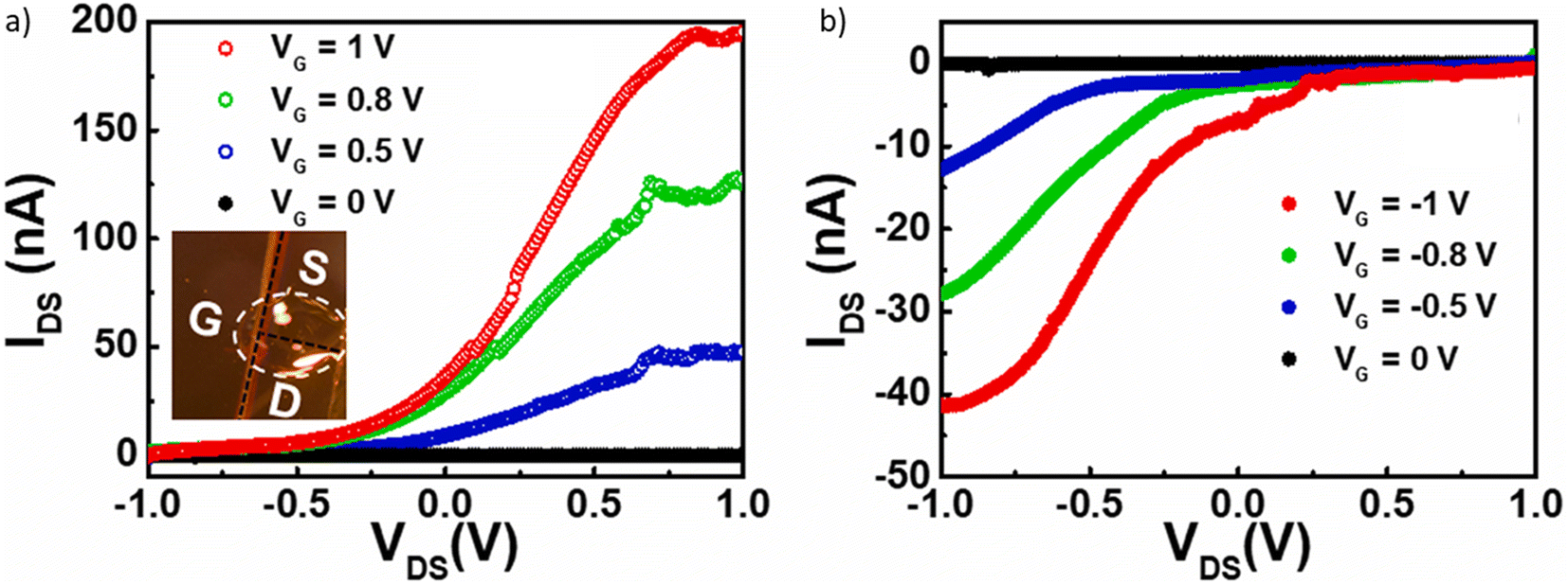 | ||
| Fig. 28 The drain-source current (IDS) versus drain-source voltage (VDS) for the FET fabricated using the film annealed at 650 °C under (a) positive and (b) negative gate voltages (VG). (a) and (b) Reproduced with permission.93 Copyright 2021, American Chemical Society. | ||
4.4. Photovoltaic
Chalcogenide perovskites have primarily garnered attention for light-emitting diode and photovoltaic applications, largely because lead-halide perovskites have dominated these two areas. BaZrS3, in particular, has attracted interest within the photovoltaic community due to its suitable bandgap for tandem solar cell applications and its theoretically estimated exceptional optoelectronic properties. However, challenges related to finding suitable substrates, high-temperature synthesis, poor film morphology, and mediocre optoelectronic properties have hindered researchers from developing solar cells without first optimizing these variables. Nishigaki et al. proposed a hybrid perovskite/c-Si monolithic two-terminal tandem solar cell architecture for BaZrS3, Ba(Zr,Ti)S3, and BaZr(S,Se)3, given the successful demonstration of high efficiencies in halide perovskite/c-Si tandem solar cells (see Fig. 29a). They calculated the maximum achievable efficiencies as a function of the perovskite layer thickness using their measured absorption coefficients, blackbody radiation, and the solar AM 1.5 spectrum. Although their estimation of the bandgap for BaZrS3 was slightly higher than typically reported, they found that BaZrS3 could achieve a maximum efficiency of around 35%. For Ba(Zr0.95Ti0.05)S3, the maximum efficiency was around 38.7% with an absorber thickness of 550 nm, an estimated Voc of 2.11 V, a Jsc of 20.6 mA cm−2, and a fill factor of 0.888. Similarly high efficiencies were calculated for Se-alloyed BaZrS3, although with much thicker films (shown in Fig. 29b).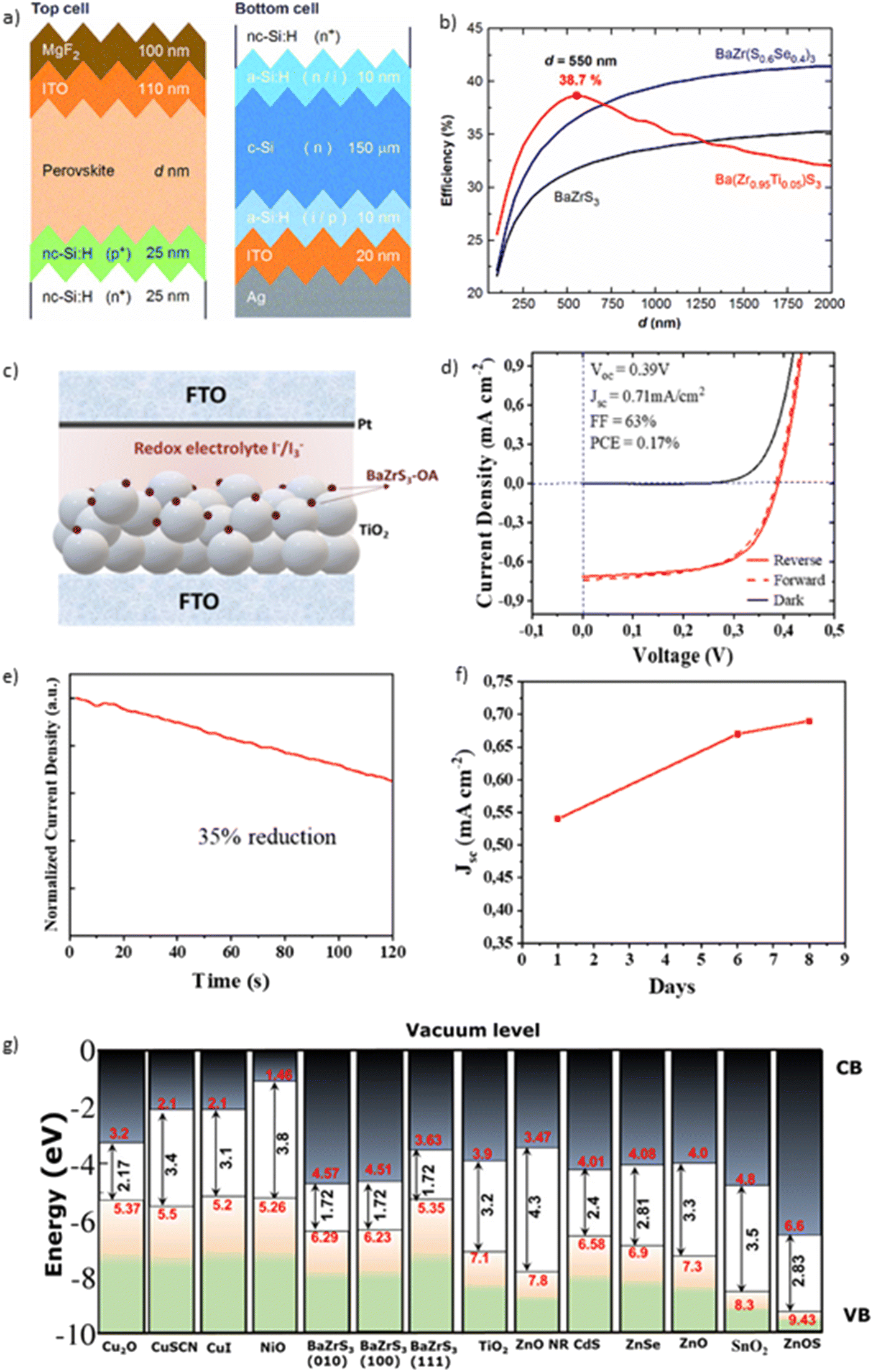 | ||
| Fig. 29 Modeling and experimental performance of BaZrS3 solar cells. (a) and (b) Proposed configuration of a perovskite-silicon tandem solar cell and the calculated device efficiencies. (a) and (b) Reproduced with permission.67 Copyright 2020, Wiley. (c) Configuration of a BaZrS3 solar cell in a dye-sensitized architecture. (d) J–V characteristics for the synthesized solar cell. (e) Maximum power point tracking at VMPP. (f) Stability of current density over several days. (c)–(f) Reproduced with permission.167 Copyright 2024, Elsevier. (g) Estimated band positions of different planes of BaZrS3 along with potential electron transport layers (ETLs) and hole transport layers (HTLs). (g) Reproduced with permission.168 Copyright 2023, American Chemical Society. | ||
Overcoming the challenges with thin-film fabrication, Dallas et al. successfully synthesized the first working solar cell using BaZrS3, employing a dye-sensitized solar cell architecture with an I−/I3− redox electrolyte in an organic solvent and a Pt cathode (see Fig. 29c).167 Following Ravi et al.'s approach, they prepared a colloidal suspension of solid-state nanoparticles, capped with oleylamine ligands and dispersed in chloroform. This dispersion was drop-cast onto a layer of mesoporous TiO2 on an FTO transparent glass substrate and annealed at various temperatures (120 °C, 200 °C, and 350 °C) to remove excess solvent. They also tested a NaS/S redox couple in H2O but achieved no reasonable current in the completed devices, suggesting that the BaZrS3 particles decomposed or hydrolyzed in water. Nonetheless, their completed devices with the I−/I3− redox couple demonstrated some charge separation and collection, reporting an average device efficiency of 0.11% with a maximum efficiency of 0.17%. The devices exhibited a short circuit current of 0.71 mA cm−2, an open circuit voltage of 0.39 V, and a fill factor of 63% under 1-sun illumination (shown in Fig. 29d). While the efficiencies varied slightly with the annealing temperature, they remained within the same range.167 Furthermore, their device demonstrated significant stability over time, as illustrated in Fig. 29e and f. This does not fully demonstrate the potential of chalcogenide perovskites, especially BaZrS3, but it highlights the need for further optimization of the material and device architecture.
To fully unlock the potential of BaZrS3, it is crucial to utilize a thin-film solar cell architecture. However, there has been limited research on the surface and interfacial properties of BaZrS3. Eya et al. studied various surface terminations, identifying the (001), (100), and (111) surfaces with S–S, S–S, and S–Ba terminations, respectively, as the most stable.168 They further performed ionization energy and electron affinity calculations for these surfaces and found that the (111) surface forms favorable alignments and optimal band offsets with many electron and hole transport materials (ETLs and HTLs) used in perovskite solar cells (depicted in Fig. 29g). According to their calculations, TiO2, ZnSe, and ZnO are promising electron transport layers due to their low conduction band offsets at the BaZrS3(111)/ETL interface. Similarly, NiO and CuI are attractive options for hole transport layers.168 However, to date, there has been no experimental verification or utilization of these transport layers. Nonetheless, several SCAPS modeling studies have been conducted to simulate solar cell architectures using BaZrS3. Researchers have explored various architectures, but these simulations often rely on several assumptions about the properties of BaZrS3, which are still under investigation in many cases.169–175 Therefore, while these studies are useful, they still await a definitive assessment of the performance or potential of BaZrS3-based solar cells.
4.5. Thermoelectrics
BaZrS3 shows promise for thermoelectric applications due to its high Seebeck coefficient and low thermal conductivity. Through first-principles calculations, Osei-Agyemang et al. determined an effective Seebeck coefficient of 3000 μV K−1 and an ultralow thermal conductivity of 1.16 W m−1 K−1 at 300 K, resulting in a thermoelectric figure of merit (zT) around 1 at 300 K, which supports the potential of BaZrS3 as a thermoelectric material. They noted that a high ZT is achieved at carrier concentrations around 1015–1018 cm−3, as higher concentrations lead to a decrease in the Seebeck coefficient. As temperature increased, thermal conductivity also increased, causing zT to drop below 1.176,177 Gupta et al. also reported extremely low conductivity for BaZrS3, with their calculations indicating an enhancement in the Seebeck coefficient and a decrease in thermal conductivity with increasing temperature. Below 500 K, zT decreased with increasing concentration.62Yang et al. experimentally confirmed the superior thermoelectric performance of BaZrS3.66 They synthesized BaZrS3 powders and converted them into dense bulks through spark plasma sintering, measuring the electronic and thermoelectric properties (see Fig. 30a–f). They found that the samples were electrically insulating at low sintering temperatures, preventing measurement of the Seebeck coefficient, but showed high n-type conductivity at high sintering temperatures (about 1600 °C) due to sulfur vacancies. The conductivity increased sharply by 5 orders of magnitude as the sintering temperature rose from 1000 °C to 1600 °C. For the optimized sintering temperature of 1600 °C, the Seebeck coefficient decreased while electrical conductivity increased as the sulfurization time of BaZrS3 powder increased from 4 to 12 hours. This increase in conductivity was likely due to increased carrier concentration from higher sulfur deficiency. The negative Seebeck coefficient indicated n-type conductivity with electrons as the majority carriers, as expected due to shallow sulfur vacancies. As sulfurization time increased from 4 to 12 hours, carrier concentration rose to 1.02 × 1019 cm−3, while carrier mobility decreased from 385 to 104 cm2 V−1 s−1. Nonetheless, these are the highest reported mobility values for BaZrS3, comparable to lead halide perovskites. The authors attributed these high mobility values to improved and optimized synthesis conditions. A low thermal conductivity of 1.74–1.82 W m−1 K−1 was achieved at room temperature due to the intrinsic structure of BaZrS3 and high sulfur deficiency, decreasing to 1.11–1.2 W m−1 K−1 at 623 K. Consequently, the zT value increased with sulfurization time, reaching a maximum of 0.37 at 623 K for BaZrS3 sulfurized for 12 hours. This experimental zT value for BaZrS3 is among the highest reported for sulfide materials (Fig. 30f).
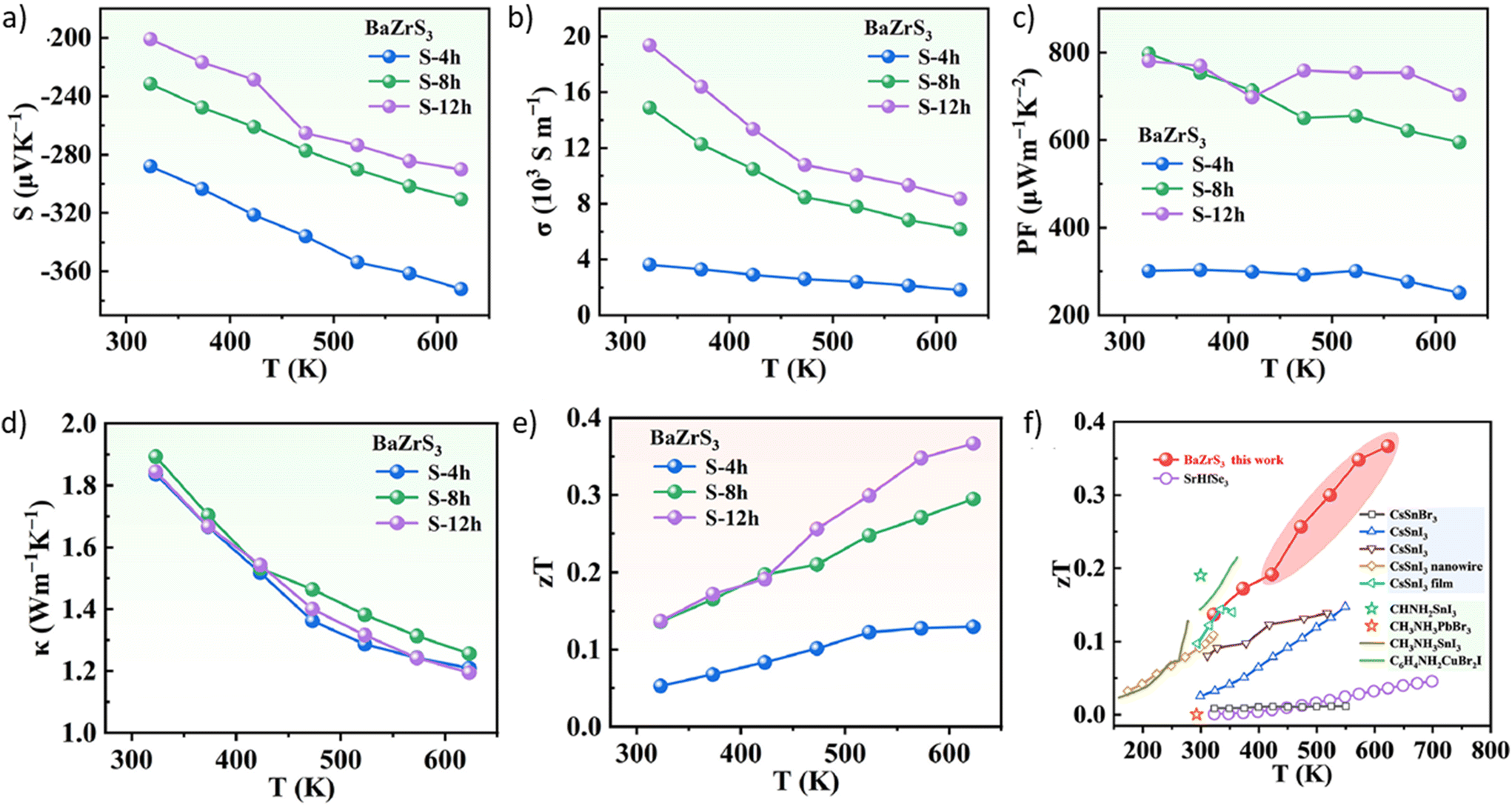 | ||
| Fig. 30 Thermoelectric performance of BaZrS3. (a)–(f) Seebeck coefficient (S), electrical conductivity (σ), power factor (PF), thermal conductivity (k), and thermoelectric efficiency (zT) as functions of annealing temperature for dense BaZrS3 bulk samples. (a)–(f) Reproduced with permission.66 Copyright 2024, Elsevier. | ||
Furthermore, Li et al. investigated the thermoelectric properties of BaZrS3 under pressure and observed a non-linear relationship with pressure due to the irregular variation of the phonon lifetime. They found that the band effective mass and degeneracy decrease, leading to a reduction in the Seebeck coefficient and an increase in electrical conductivity, ultimately reducing the power factor and zT, indicating that the thermoelectric performance of BaZrS3 degrades under pressure.178 Wu et al. attributed the low thermal conductivity in BaZrS3 to weak bonding and strong anharmonicity, suggesting that the thermoelectric performance of BaZrS3 can be improved by alloying with Se or Ti.179
These computational and experimental observations suggest a promising future for BaZrS3 in thermoelectrics. Its thermoelectric performance could also be modified through alloying, doping, nanostructuring, or other strategies.
4.6. Spintronics
Spintronic applications require semiconductor materials with specific properties that enable the manipulation and detection of electron spin states. Semiconductors that exhibit ferromagnetism or can be magnetized are particularly beneficial for spintronic devices, as they combine magnetic and semiconducting properties. To achieve such materials, transition metals are often doped into parent materials to induce magnetism. Yu et al. investigated doping BaZrS3 with up to 5% Mn and Fe, aiming to develop a new magnetic semiconductor. The authors observed that Mn and Fe can be doped at the Zr site up to 5% without forming secondary phases and noted a monotonic decrease in bandgap with increasing doping levels. The level of magnetization also increased with doping. While Mn-doped samples exhibited paramagnetic behavior at room temperature, Fe-doped samples showed ferromagnetism. Nevertheless, further research is required to elucidate the mechanisms by which Mn and Fe doping induces magnetism, to comprehensively characterize the resulting magnetic properties, and to explore the potential of BaZrS3 for applications that leverage these properties.180Recently, Yaghoubi et al. employed density functional theory (DFT) calculations to identify two previously unreported phases of BaZrS3, designated as Pna21 and Pmc21, which have not yet been experimentally observed.181 They noted that these phases exhibit powder X-ray diffraction patterns and Raman spectra that closely resemble those of the widely studied Pnma phase. However, subtle distinctions in Laue diffraction patterns were identified as a potential method for differentiating these phases.
The authors further demonstrated that the non-polar Pnma phase lacks ferroelectric behavior, whereas their calculations suggest that the Pna21 and Pmc21 phases exhibit weak ferroelectric properties, with ionic and electronic polarizations nearly canceling each other. They also proposed that the application of strain could enhance the ferroelectric characteristics of these phases, suggesting that strain engineering may provide a viable experimental approach for observing them.
If validated experimentally, this discovery could hold significant promise for BaZrS3, as ferroelectric behavior in solar cell materials is known to enhance charge separation and potentially improve photovoltaic efficiency. These findings open exciting new avenues for the application of BaZrS3 in advanced optoelectronic and energy-harvesting devices.
4.7. Piezoelectricity
Semiconductor materials are also frequently utilized as piezoelectric materials, where an electric charge is generated in response to applied pressure. This phenomenon arises from the intrinsic crystal structure of these materials, which lack a center of symmetry. When mechanical stress is applied, it causes a displacement of the positive and negative charge centers within the crystal, resulting in an electric dipole moment and the generation of an electric charge on the surface.While BaZrS3 typically exhibits a centrosymmetric structure (which is generally non-polar and weakly piezoelectric), first-principles calculations by Abir et al. indicate that it has a loosely packed unit cell with significant vacant space.182 This allows for an extended displacement of ions, resulting in a displacement-mediated dipole moment. Similar piezoelectric behavior is not observed in centrosymmetric BaZrO3 due to its tightly packed unit cell. The significance of the piezoresponse in BaZrS3 lies in the abundance and non-toxicity of its elements, contrasting with other commonly used piezoelectric materials.
For 300 nm BaZrS3 films deposited on quartz, Abir et al. observed a strong piezoelectric response of ∼21.38 ± 1.51 pm V−1 (picometers per volt) through Piezoresponse Force Microscopy (PFM), where the amplitude increased with increasing voltage. This piezoresponse of BaZrS3 is comparable to other piezoelectric materials. This experimental result for BaZrS3 aligns with piezoresponse values calculated through first-principles Density Functional Perturbation Theory (DFPT). Interestingly, the calculated piezoresponse for BaHfS3 is even higher, around 102.58 pm V−1 (for d21), making it a promising candidate for piezoelectric applications.182
Abir et al. also demonstrated practical devices exhibiting piezoelectric behavior by creating a composite matrix of BaZrS3 powder dispersed in polymer (Polycaprolactone: PCL), which provides ductility for energy harvesting materials. They completed the device by attaching Cu electrodes to the top and bottom surfaces of the polymer film. Testing various loadings of BaZrS3 in the polymer, they found that the optimal performance was achieved with 15% loading, as higher percentages led to agglomeration and disconnection from the polymer matrix, reducing response. The device yielded a peak output of ∼103.5 μW cm−2, surpassing some of the best-performing piezoelectric materials. Abir et al. successfully demonstrated the charging of capacitors and lighting of LEDs through body movements while wearing their flexible piezoelectric device.182
These findings highlight a significant application for BaZrS3. Future research could focus on inducing defects in the material, breaking centrosymmetry, and amplifying the piezoresponse to further enhance its performance.
5. Future challenges and outlook
BaZrS3 has emerged as an exciting, non-toxic absorber material for photovoltaic applications (Table 4 summarizes the properties of BaZrS3). Composed of earth-abundant elements, it is expected to benefit from its perovskite crystal structure. Despite advancements in reducing synthesis temperatures, developing various deposition methods, and experimentally verifying its promising absorption coefficient, further work is needed in the following areas to fully demonstrate its potential:1. BaZrS3 has been synthesized using various methods, including sputtering, pulsed laser deposition, molecular beam epitaxy, and solution processing. However, limited work has been done on optimizing the composition of the final film, leading to inconsistent compositions across the literature. This inconsistency has made it challenging to assess the role of composition accurately. A barium-deficient composition might result in barium-related defects, such as VBa or ZrBa, which could impact the optical and electronic properties. In our previous work, we demonstrated that BaZrS3 does not decompose into binaries until the Ba ratio is approximately 0.7. Conversely, barium-rich compositions might lead to undetected amorphous secondary phases in the film, significantly affecting its properties. Therefore, accurate composition determination is crucial for correlating composition with optical and electrical properties. While techniques like energy-dispersive X-ray spectroscopy are frequently used, determining the correct composition without a BaZrS3 standard is challenging due to overlapping peaks. Thus, exploring other accessible composition analysis techniques is essential. Inductively Coupled Plasma Optical Emission Spectroscopy (ICP-OES) could be one such method, as it can accurately provide the bulk composition, assuming all constituent elements from the film are soluble in a common solvent, typically a dilute acid. However, co-dissolving Ba and S in any dilute acid has been challenging due to the formation of insoluble BaSO4 species.
2. Once a method to accurately measure composition is established, it is essential to study the effect of composition on electrical and optical properties. In sulfur-poor conditions, sulfur vacancies easily form, potentially leading to a very high electron concentration, which is undesirable for a solar absorber. Conversely, sulfur-rich conditions could result in deep sulfur interstitial defects. A barium-poor composition film grown in a sulfur-poor environment might balance out the excess electrons, thereby reducing excess carrier concentrations. Therefore, there is a need to grow films under various sulfur environments with different metal ratios to optimize the properties of BaZrS3 as a solar absorber.
3. It is important to synthesize BaZrS3 at temperatures below 600 °C to integrate with other layers of a solar cell, which likely cannot withstand higher temperatures. Although solution-processing methods and sputtering-based techniques have achieved low-to-moderate temperature synthesis of BaZrS3, these methods have shown limited control over material quality. Notably, these methods have reported no photoluminescence in the films, which is concerning. Since most of these methods were conducted in sulfur-rich environments, sulfur interstitials may have formed, quenching the photoluminescence. Additionally, sulfur-poor growth conditions in some methods have resulted in Ruddlesden–Popper impurities, indicating a need for careful optimization of growth conditions at low temperatures. Furthermore, nanoparticles grown by Zilevu et al.136 did not exhibit photoluminescence, while those by Yang et al.135 displayed an unnatural blue-shifted photoluminescence peak, potentially arising from secondary phases or organic residues. Importantly, the electrical transport properties of these methods have not been measured and need to be tested and optimized. Overall, low-temperature growth methods are crucial for exploring BaZrS3 in solar cells, but significant work is required to improve and optimize their growth conditions and properties. A low-temperature photoluminescence (PL) study can be performed to investigate the presence of midgap defect transitions. For nanoparticles, conducting a ligand exchange to a more suitable organic or ionic ligand could effectively passivate surface defects, thereby enhancing photoluminescence efficiency.
4. Another significant bottleneck is the overgrowth of grains in methods relying on liquid flux. Solution-processed BaZrS3 films have not been found to nucleate on a hotplate in an inert environment at temperatures below 500 °C, unlike other chalcogenides such as Cu(In,Ga)S2 and Cu2ZnSnS4. This limitation necessitates an additional sulfurization step, where the amorphous film, consisting of a Ba–Zr–S matrix, is sulfurized in the presence of excess sulfur. This process relies on the formation of BaSx liquid flux, which apparently does not produce many nucleation sites and causes Ostwald ripening, resulting in large, disconnected grains. Consequently, synthesizing a smooth film with well-connected grains of BaZrS3 through solution-processing methods has been challenging. While methods utilizing sulfurization under CS2 at high temperatures have achieved reasonable film continuity, they have not attained satisfactory grain growth. Therefore, optimizing growth conditions and creating additional nucleation sites during sulfurization could be crucial for achieving smooth, contiguous films. This outcome could potentially be achieved through a multi-temperature sulfurization process.
5. To successfully implement BaZrS3 in a thin-film solar cell architecture, the films must be deposited on a conductive substrate. Alternatively, they could be transferred using a conductive epoxy lift-off to a substrate of choice. However, limited work has been done on the former approach, with only one report on BaZrS3 synthesis on a molybdenum substrate, which produced a film with small grain size and significant sulfurization of the Mo contact into a MoS2 layer, which is not ideal. There does not appear to be a suitable conductive substrate that can withstand corrosive sulfur environments at high temperatures. Similarly, moderate temperatures with long annealing times are also not favorable. While some conductive substrates, such as gold, might be more tolerant to degradation, they would negate the cost and abundance benefits of BaZrS3. A more thoughtful solution is required to address this challenge effectively. Potential approaches may include the development of low-sulfur-pressure-based annealing methods or the transfer of the synthesized film onto a conductive substrate using a lift-off technique.
6. The optical quality of BaZrS3 grown by various methods has consistently fallen short of expectations. While CS2-based sulfurization methods have yielded films with reasonable photoluminescence, the FWHM of the peaks has been significantly higher compared to lead halide perovskites, indicating substantial defects, disorders, and inhomogeneities within the material. Moreover, there are no reported values of PLQY for BaZrS3. Transient photoluminescence studies on BaZrS3 films and single crystals have shown a fast initial decay followed by a slow decay, further suggesting defect-mediated recombinations. Additionally, other sulfurization methods, including those involving low-temperature synthesis, have produced films with either very broad, low-quality photoluminescence or no photoluminescence at all. This points to a recurring issue of material quality and defect-related problems across all synthesis methods. Yuan et al. described that oxygen-related point defects do not lead to deep states within the bandgap of BaZrS3.122 Therefore, the argument that CS2, being more reactive at high temperatures than sulfur or H2S, would more effectively remove oxygen impurities and thus improve properties may not be valid and requires experimental verification. Even films grown by molecular beam epitaxy have not shown exceptional photoluminescence or photoconductivity, casting doubt on the intrinsic properties of the material. There are also not many reports characterizing the photoluminescence spectra of BaZrS3 across the full wavelength range, as we reported a PL peak at around 1.1 eV in all the solution-deposited films and synthesized solid-state powders irrespective of the flux used.123 It is difficult to say if it appeared because of some recurring impurity (such as a Ruddlesden Popper phase) or if it is a midgap defect. Hence, a more detailed investigation is needed to improve the bulk material quality and passivate the surfaces.
7. The transport properties of BaZrS3 have not shown significant promise. Most literature reports n-type conductivity for BaZrS3, attributed to shallow sulfur vacancy defects contributing electrons to the conduction band. These shallow defects, which have low formation energy, combined with sulfur-poor growth conditions at high annealing temperatures, have resulted in extremely high carrier concentrations. Such high carrier concentrations are not ideal for a solar absorber in a typical p–n junction architecture and may lead to unwanted Auger recombinations. Therefore, controlling carrier concentrations through engineering growth conditions, adjusting composition, or implementing extrinsic doping is necessary. Extrinsic doping with elements that can introduce holes to the valence band without creating unwanted mid-gap defects would be ideal, as they can reduce electron concentrations or potentially change the conductivity type with extensive doping. Possible dopants include alkali metals such as Na, K, and La, among others. While the highest carrier mobilities observed for BaZrS3 are comparable to other chalcogenides like Cu(In,Ga)Se2, they are an order of magnitude lower than those for halide perovskites. These mobilities could be limited by unoptimized films with bulk defects, imperfections, small grains with unpassivated grain boundaries, surface states, non-ideal composition, high doping levels, and impurities. Therefore, significant work is needed to address these issues and improve the carrier properties of BaZrS3.
8. Recent studies have successfully alloyed BaZrS3 with Ti, Se, and Hf, exploring a range of bandgaps from 1.3 eV to 2.1 eV. This makes these alloyed absorbers promising candidates for single-junction and tandem solar cell applications. However, most research has focused on synthesizing solid-state powders, with only a few reports on thin films and limited characterizations. Therefore, more comprehensive optical and electronic characterizations are needed to evaluate the absorber quality of these films fully. Other candidates for A-site and B-site alloying, such as Sr, Eu, Mo, Nb, Ta and W, should be explored and studied.
9. The limitations in the material quality of BaZrS3 have hindered the PV community from fabricating solar cells from BaZrS3 and utilizing it for other applications. Dallas et al. made significant progress by employing a dye-sensitized solar cell architecture for BaZrS3.167 While it is promising to observe some photocurrent and a decent open-circuit voltage, a proper thin-film device architecture is required to unlock the full potential of BaZrS3 for photovoltaic applications. Eya et al. also estimated the band positions of different BaZrS3 crystal planes and suggested various hole and electron transport layers.168 However, no substantial work has been done to experimentally confirm the band positions of BaZrS3. Therefore, it is crucial to experimentally determine the band positions and identify the junction partners that are compatible with BaZrS3 and other layers to ensure efficient device integration.
10. While the focus is on utilizing BaZrS3 for tandem solar cells, its other exciting properties should also be leveraged for various applications such as thermoelectric, piezoelectric, resistive switching memories, anodes in batteries, gas sensors, X-ray detectors, among others.
| Property of BaZrS3 | Reported values |
|---|---|
| Bandgap (eV) | 1.74 (ref. 40), 1.75 (ref. 62), 1.82 (ref. 86), 1.85 (ref. 105), 1.89 (ref. 93), 1.9 (ref. 89), 1.94 (ref. 67), 2.23 (ref. 48) |
| Electron affinity (eV) | (4.57 (010), 4.51 (100), 3.63 (111)) (ref. 168) |
| Ionization potential (eV) | (6.29 (010), 6.23 (100), 5.35 (111)) (ref. 168) |
| Dielectric constant | 76.2 (ref. 69), 46 (ref. 183) |
| Electron mobility (cm2 V−1 s−1) | 385 (ref. 66), 13.7 (ref. 86), 16.8 (ref. 93), 1 (ref. 153) |
| Hole mobility (cm2 V−1 s−1) | 2.6 (ref. 93), 30 (ref. 48) |
| Electron effective mass | 0.3 (ref. 184), 0.43 (ref. 70), 0.318 (ref. 59), 0.3 (ref. 122) |
| Hole effective mass | 0.46 (ref. 184), 0.75 (ref. 70), 0.459 (ref. 59), 0.9 (ref. 86 and 122) |
| Carrier density (cm−3) | (1019–1020) (ref. 86), 4.4 × 10¹⁰ (ref. 93), >1020 (ref. 153), 1.102 × 10¹⁹ (ref. 66), 1018 (ref. 48) |
| Extinction coefficient | 1.7 (ref. 168) |
| Absorption coefficient (cm−1) | 105 (ref. 168), ∼105 (ref. 67), ∼105 (ref. 68) |
| Work function | (6.20 (010), 5.624 (100), 5.109 (111)) (ref. 168), 4.44 (ref. 146) |
| Reflectivity | 22% (ref. 168) |
| Refractive index | 2.75 (ref. 168) |
| Seebeck coefficient (μV K−1) | 3000 (ref. 177), ∼280 (ref. 66) |
| Thermal conductivity (W m−1 K−1) | 1.16 (ref. 177), 1.84 (ref. 179), 1.74–1.82 (ref. 66) |
| zT | 0.58 (ref. 179), ∼1 (ref. 177), (0.37 at 600 K, 0.14 at 300 K) (ref. 66) |
| Heat capacity (J g−1 K−1) | 100 (ref. 177) |
BaZrS3 remains an exciting, earth-abundant candidate for photovoltaics and other applications. Over the past 5–6 years, a surge of synthesis methods has significantly reduced the synthesis temperature. There is now an improved understanding of the transport properties, stability, and defect characteristics of the material. However, key challenges persist, including high carrier concentration, inconsistent optoelectronic properties, and the synthesis of a contiguous film with large, connected grains on a conductive substrate. It is expected that the overview of BaZrS3 and the potential strategies for future work presented in this review will aid towards the development and utilization of this class of materials.
Data availability
No data were used for the research described in the article.Conflicts of interest
The authors declare that there are no known competing conflicts of interests.Acknowledgements
This work was supported by the NSF program 10001536 (INFEWS).References
- I. Shahbaz, M. Tahir, L. Li and Y. Song, Advancements in 2D Transition Metal Dichalcogenides (TMDs) Inks for Printed Optoelectronics: A Comprehensive Review, Mater. Today, 2024, 77, 142–184, DOI:10.1016/j.mattod.2024.06.008.
- O. S. Chaudhary, M. Denaï, S. S. Refaat and G. Pissanidis, Technology and Applications of Wide Bandgap Semiconductor Materials: Current State and Future Trends, Energies, 2023, 16(18), 6689, DOI:10.3390/en16186689.
- H. Dong, C. Ran, W. Gao, M. Li, Y. Xia and W. Huang, Metal Halide Perovskite for Next-Generation Optoelectronics: Progresses and Prospects, eLight, 2023, 3(1), 3, DOI:10.1186/s43593-022-00033-z.
- Z. Guo, J. Zhang, X. Liu, L. Wang, L. Xiong and J. Huang, Optoelectronic Synapses and Photodetectors Based on Organic Semiconductor/Halide Perovskite Heterojunctions: Materials, Devices, and Applications, Adv. Funct. Mater., 2023, 33(46), 2305508, DOI:10.1002/adfm.202305508.
- S. Song, M. Rahaman and D. Jariwala, Can 2D Semiconductors Be Game-Changers for Nanoelectronics and Photonics?, ACS Nano, 2024, 18(17), 10955–10978, DOI:10.1021/acsnano.3c12938.
- B. Ghosh, D. J. J. Tay, M. B. J. Roeffaers and N. Mathews, Lead-Free Metal Halide (Halogenidometallate) Semiconductors for Optoelectronic Applications, Appl. Phys. Rev., 2023, 10, 031312, DOI:10.1063/5.0150873.
- N. Li, S. Zhang, Y. Peng, X. Li, Y. Zhang, C. He and G. Zhang, 2D Semiconductor–Based Optoelectronics for Artificial Vision, Adv. Funct. Mater., 2023, 33(52), 2305589, DOI:10.1002/adfm.202305589.
- P. Verlinden, D. L. Young, G. Xiong, M. O. Reese, L. M. Mansfield, M. Powalla, S. Paetel, R. M. France, P. T. Chiu and N. M. Haegel, Photovoltaic Device Innovation for a Solar Future, Device, 2023, 1(1), 100013, DOI:10.1016/j.device.2023.100013.
- A. Rauf, N. Nureen, M. Irfan and M. Ali, The Current Developments and Future Prospects of Solar Photovoltaic Industry in an Emerging Economy of India, Environ. Sci. Pollut. Res., 2023, 30(16), 46270–46281, DOI:10.1007/s11356-023-25471-1.
- A. Urbina, Sustainability of Photovoltaic Technologies in Future Net–zero Emissions Scenarios, Prog. Photovolt. Res. Appl., 2023, 31(12), 1255–1269, DOI:10.1002/pip.3642.
- J. Liu, M. De Bastiani, E. Aydin, G. T. Harrison, Y. Gao, R. R. Pradhan, M. K. Eswaran, M. Mandal, W. Yan, A. Seitkhan, M. Babics, A. S. Subbiah, E. Ugur, F. Xu, L. Xu, M. Wang, A. u. Rehman, A. Razzaq, J. Kang, R. Azmi, A. A. Said, F. H. Isikgor, T. G. Allen, D. Andrienko, U. Schwingenschlögl, F. Laquai and S. De Wolf, Efficient and Stable Perovskite-Silicon Tandem Solar Cells through Contact Displacement by MgFx, Science, 2022, 377(6603), 302–306, DOI:10.1126/science.abn8910.
- H. Li and W. Zhang, Perovskite Tandem Solar Cells: From Fundamentals to Commercial Deployment, Chem. Rev., 2020, 120(18), 9835–9950, DOI:10.1021/acs.chemrev.9b00780.
- A. W. Y. Ho-Baillie, J. Zheng, M. A. Mahmud, F.-J. Ma, D. R. McKenzie and M. A. Green, Recent Progress and Future Prospects of Perovskite Tandem Solar Cells, Appl. Phys. Rev., 2021, 8, 041307, DOI:10.1063/5.0061483.
- S. D. B. George, A. Soosaimanickam and S. Sundaram, Third-Generation Photovoltaics: Introduction, Overview, Innovation, and Potential Markets, in Photovoltaics Beyond Silicon, Elsevier, 2024, pp. 75–110. DOI:10.1016/B978-0-323-90188-8.00020-8.
- P. J. Dale and M. A. Scarpulla, Efficiency versus Effort: A Better Way to Compare Best Photovoltaic Research Cell Efficiencies?, Sol. Energy Mater. Sol. Cells, 2023, 251, 112097, DOI:10.1016/j.solmat.2022.112097.
- J. Werner, B. Niesen and C. Ballif, Perovskite/Silicon Tandem Solar Cells: Marriage of Convenience or True Love Story? – An Overview, Adv. Mater. Interfaces, 2018, 5(1), 1700731, DOI:10.1002/admi.201700731.
- M. Yamaguchi, K.-H. Lee, K. Araki and N. Kojima, A Review of Recent Progress in Heterogeneous Silicon Tandem Solar Cells, J. Phys. D: Appl. Phys., 2018, 51(13), 133002, DOI:10.1088/1361-6463/aaaf08.
- N. N. Lal, Y. Dkhissi, W. Li, Q. Hou, Y. Cheng and U. Bach, Perovskite Tandem Solar Cells, Adv. Energy Mater., 2017, 7(18), 1602761, DOI:10.1002/aenm.201602761.
- M. K. Rao, D. N. Sangeetha, M. Selvakumar, Y. N. Sudhakar and M. G. Mahesha, Review on Persistent Challenges of Perovskite Solar Cells’ Stability, Sol. Energy, 2021, 218, 469–491, DOI:10.1016/j.solener.2021.03.005.
- J.-P. Correa-Baena, M. Saliba, T. Buonassisi, M. Grätzel, A. Abate, W. Tress and A. Hagfeldt, Promises and Challenges of Perovskite Solar Cells, Science, 2017, 358(6364), 739–744, DOI:10.1126/science.aam6323.
- S. J. Adjogri and E. L. Meyer, Chalcogenide Perovskites and Perovskite-Based Chalcohalide as Photoabsorbers: A Study of Their Properties, and Potential Photovoltaic Applications, Materials, 2021, 14(24), 7857, DOI:10.3390/ma14247857.
- R. Raj, R. Singh and M. Guin, Chalcogenide Perovskite, An Emerging Photovoltaic Material: Current Status and Future Perspectives, ChemistrySelect, 2023, 8(45), e202303550, DOI:10.1002/slct.202303550.
- K. V. Sopiha, C. Comparotto, J. A. Márquez and J. J. S. Scragg, Chalcogenide Perovskites: Tantalizing Prospects, Challenging Materials, Adv. Opt. Mater., 2022, 2101704, DOI:10.1002/adom.202101704.
- M. Ju, J. Dai, L. Ma and X. C. Zeng, Perovskite Chalcogenides with Optimal Bandgap and Desired Optical Absorption for Photovoltaic Devices, Adv. Energy Mater., 2017, 7(18), 1700216, DOI:10.1002/aenm.201700216.
- Y.-Y. Sun, M. L. Agiorgousis, P. Zhang and S. Zhang, Chalcogenide Perovskites for Photovoltaics, Nano Lett., 2015, 15(1), 581–585, DOI:10.1021/nl504046x.
- D. Tiwari, O. S. Hutter and G. Longo, Chalcogenide Perovskites for Photovoltaics: Current Status and Prospects, J. Phys.: Energy, 2021, 3(3), 034010, DOI:10.1088/2515-7655/abf41c.
- W. Li, S. Niu, B. Zhao, R. Haiges, Z. Zhang, J. Ravichandran and A. Janotti, Band Gap Evolution in Ruddlesden-Popper Phases, Phys. Rev. Mater., 2019, 3(10), 101601, DOI:10.1103/PhysRevMaterials.3.101601.
- S. Niu, B. Zhao, K. Ye, E. Bianco, J. Zhou, M. E. McConney, C. Settens, R. Haiges, R. Jaramillo and J. Ravichandran, Crystal Growth and Structural Analysis of Perovskite Chalcogenide BaZrS3 and Ruddlesden–Popper Phase Ba3Zr2S7, J. Mater. Res., 2019, 34(22), 3819–3826, DOI:10.1557/jmr.2019.348.
- H. Shahmohamadi and S. S. Naghavi, Sulfide Perovskites for Thermoelectricity, ACS Appl. Mater. Interfaces, 2021, 13(12), 14189–14197, DOI:10.1021/acsami.0c22842.
- T. R. Paudel and E. Y. Tsymbal, Evaluating the Thermoelectric Properties of BaTiS3 by Density Functional Theory, ACS Omega, 2020, 5(21), 12385–12390, DOI:10.1021/acsomega.0c01139.
- J. H. A. Shuhaib, J. F. Fernández, J. Bodega, J. R. Ares, I. J. Ferrer and F. Leardini, Synthesis, Optical Band Gap and Thermoelectric Properties of Sr1+xTiS3−y Chalcogenide Perovskites, Mater. Res. Bull., 2023, 167, 112405, DOI:10.1016/j.materresbull.2023.112405.
- W. Feng, R. Zhao, X. Wang, B. Xing, Y. Zhang, X. He and L. Zhang, Global Instability Index as a Crystallographic Stability Descriptor of Halide and Chalcogenide Perovskites, J. Energy Chem., 2022, 70, 1–8, DOI:10.1016/j.jechem.2022.02.018.
- A. Swarnkar, W. J. Mir, R. Chakraborty, M. Jagadeeswararao, T. Sheikh and A. Nag, Are Chalcogenide Perovskites an Emerging Class of Semiconductors for Optoelectronic Properties and Solar Cell?, Chem. Mater., 2019, 565–575, DOI:10.1021/acs.chemmater.8b04178.
- Y. Peng, Q. Sun, H. Chen and W.-J. Yin, Disparity of the Nature of the Band Gap between Halide and Chalcogenide Single Perovskites for Solar Cell Absorbers, J. Phys. Chem. Lett., 2019, 10(16), 4566–4570, DOI:10.1021/acs.jpclett.9b01657.
- G. F. Hüttig, Notiz Zur Geometrie Der Koordinationszahl, Z. Anorg. Allg. Chem., 1920, 114(1), 24–26, DOI:10.1002/zaac.19201140103.
- C. Li, K. C. K. Soh and P. Wu, Formability of ABO3 Perovskites, J. Alloys Compd., 2004, 372(1–2), 40–48, DOI:10.1016/j.jallcom.2003.10.017.
- W. B. Jensen and W. B. Jensen, The Origin of the Ionic-Radius Ratio Rules, J. Chem. Educ., 2010, 87(6), 587–588, DOI:10.1021/ed100258f.
- A. M. Glazer, The Classification of Tilted Octahedra in Perovskites, Acta Crystallogr., Sect. B, 1972, 28(11), 3384–3392, DOI:10.1107/S0567740872007976.
- V. M. Goldschmidt, Die Gesetze Der Krystallochemie, Naturwissenschaften, 1926, 14(21), 477–485, DOI:10.1007/BF01507527.
- S. Perera, H. Hui, C. Zhao, H. Xue, F. Sun, C. Deng, N. Gross, C. Milleville, X. Xu, D. F. Watson, B. Weinstein, Y. Y. Sun, S. Zhang and H. Zeng, Chalcogenide Perovskites - an Emerging Class of Ionic Semiconductors, Nano Energy, 2016, 22, 129–135, DOI:10.1016/j.nanoen.2016.02.020.
- H. I. Eya, E. Ntsoenzok and N. Y. Dzade, First–Principles Investigation of the Structural, Elastic, Electronic, and Optical Properties of α- and β-SrZrS3: Implications for Photovoltaic Applications, Materials, 2020, 13(4), 978, DOI:10.3390/ma13040978.
- M. L. Han and Y. Hu, Structural, Electronic, Elastic, and Optical Properties of Chalcogenide Perovskite SrZrS3 under Ambient and High-Pressure Conditions, Chalcogenide Lett., 2023, 20(8), 619–628, DOI:10.15251/CL.2023.208.619.
- K. Hanzawa, S. Iimura, H. Hiramatsu and H. Hosono, Material Design of Green-Light-Emitting Semiconductors: Perovskite-Type Sulfide SrHfS3, J. Am. Chem. Soc., 2019, 141(13), 5343–5349, DOI:10.1021/jacs.8b13622.
- Y. Han, J. Fang, Y. Liang, H. Gao, J. Yang, X. Chen, Y. Yuan and Z. Shi, Preparation of Chalcogenide Perovskite SrHfS3 and Luminescent SrHfS3:Eu2+ Thin Films, Appl. Phys. Lett., 2024, 124, 131902, DOI:10.1063/5.0200555.
- Y. Liang, J. Li, Z. Chen, G. Li, M. Li, M. Jia, X. Chen, X. Li, Y. Han and Z. Shi, Tapping the Light Emitting Potential of Chalcogenide Perovskite SrHfS3 via Eu2+ Doping, Adv. Opt. Mater., 2024, 12(6), 2301977, DOI:10.1002/adom.202301977.
- H. Zhang, X. Wu, K. Ding, L. Xie, K. Yang, C. Ming, S. Bai, H. Zeng, S. Zhang and Y.-Y. Sun, Prediction and Synthesis of a Selenide Perovskite for Optoelectronics, Chem. Mater., 2023, 35(11), 4128–4135, DOI:10.1021/acs.chemmater.2c03676.
- J. Du, J. Shi, W. Guo, S. Liu, Y. He, C. Tian, Y. Zhu and H. Zhong, Cerium-Based Lead-Free Chalcogenide Perovskites for Photovoltaics, Phys. Rev. B, 2021, 104(23), 235206, DOI:10.1103/PhysRevB.104.235206.
- Y. Han, J. Xu, Y. Liang, X. Chen, M. Jia, J. Zhang, L. Lian, Y. Liu, X. Li and Z. Shi, P-Type, Conductive BaZrS3 Thin Film and Its Band Gap Tunning via Ruddlesden-Popper Ba3Zr2S7 and Titanium Alloying, Chem. Eng. J., 2023, 473, 145351, DOI:10.1016/j.cej.2023.145351.
- Y. Zhang, T. Shimada, T. Kitamura and J. Wang, Ferroelectricity in Ruddlesden–Popper Chalcogenide Perovskites for Photovoltaic Application: The Role of Tolerance Factor, J. Phys. Chem. Lett., 2017, 8(23), 5834–5839, DOI:10.1021/acs.jpclett.7b02591.
- S. Niu, D. Sarkar, K. Williams, Y. Zhou, Y. Li, E. Bianco, H. Huyan, S. B. Cronin, M. E. McConney, R. Haiges, R. Jaramillo, D. J. Singh, W. A. Tisdale, R. Kapadia and J. Ravichandran, Optimal Bandgap in a 2D Ruddlesden–Popper Perovskite Chalcogenide for Single-Junction Solar Cells, Chem. Mater., 2018, 30(15), 4882–4886, DOI:10.1021/acs.chemmater.8b01707.
- K. Ye, B. Zhao, B. T. Diroll, J. Ravichandran and R. Jaramillo, Time-Resolved Photoluminescence Studies of Perovskite Chalcogenides, Faraday Discuss., 2022, 239, 146–159, 10.1039/D2FD00047D.
- M. L. Agiorgousis, Y. Sun, D. Choe, D. West and S. Zhang, Machine Learning Augmented Discovery of Chalcogenide Double Perovskites for Photovoltaics, Adv. Theory Simul., 2019, 2(5), 1800173, DOI:10.1002/adts.201800173.
- Q. Sun, H. Chen and W.-J. Yin, Do Chalcogenide Double Perovskites Work as Solar Cell Absorbers: A First-Principles Study, Chem. Mater., 2019, 31(1), 244–250, DOI:10.1021/acs.chemmater.8b04320.
- M. D. Kassa, N. G. Debelo and M. M. Woldemariam, First-Principles Calculations to Investigate Small Band Gap Ca2ZrHfS6 Double Chalcogenide Perovskites for Optoelectronic Application, Indian J. Phys., 2024, 98, 1259–1270, DOI:10.1007/s12648-023-02905-7.
- A. Jess, R. Yang and C. J. Hages, On the Phase Stability of Chalcogenide Perovskites, Chem. Mater., 2022, 30(3), 679–684, DOI:10.1021/acs.chemmater.2c01289.
- J. Turnley, S. Agarwal and R. Agrawal, Rethinking Tolerance Factor Analysis for Chalcogenide Perovskites, Mater. Horiz., 2024, 11, 4802–4808, 10.1039/D4MH00689E.
- X. Wei, H. Hui, S. Perera, A. Sheng, D. F. Watson, Y.-Y. Sun, Q. Jia, S. Zhang and H. Zeng, Ti-Alloying of BaZrS3 Chalcogenide Perovskite for Photovoltaics, ACS Omega, 2020, 5(30), 18579–18583, DOI:10.1021/acsomega.0c00740.
- D. Liu, H. Peng, J. He and R. Sa, Alloy Engineering to Tune the Optoelectronic Properties and Photovoltaic Performance for Hf-Based Chalcogenide Perovskites, Mater. Sci. Semicond. Process., 2024, 169, 107919, DOI:10.1016/j.mssp.2023.107919.
- M. B. Kanoun, B. Ul Haq, A.-A. Kanoun and S. Goumri-Said, Ti Alloying as a Route to BaZrS3 Chalcogenide Perovskite with Enhanced Photovoltaic Performance, Energy Fuels, 2023, 37(13), 9548–9556, DOI:10.1021/acs.energyfuels.3c01272.
- R. Chami, A. Lekdadri, M. Chafi, L. H. Omari and E. K. Hlil, Sn-Alloying of BaZrS3 Chalcogenide Perovskite as Eco-Friendly Material for Photovoltaics: First Principle Insight, Solid State Commun., 2023, 369, 115212, DOI:10.1016/j.ssc.2023.115212.
- K. Ye, I. Sadeghi, M. Xu, J. Van Sambeek, T. Cai, J. Dong, R. Kothari, J. M. LeBeau and R. Jaramillo, A Processing Route to Chalcogenide Perovskites Alloys with Tunable Band Gap via Anion Exchange, Adv. Funct. Mater., 2024, 34(44), 2405135, DOI:10.1002/adfm.202405135.
- T. Gupta, D. Ghoshal, A. Yoshimura, S. Basu, P. K. Chow, A. S. Lakhnot, J. Pandey, J. M. Warrender, H. Efstathiadis, A. Soni, E. Osei-Agyemang, G. Balasubramanian, S. Zhang, S. Shi, T. Lu, V. Meunier and N. Koratkar, An Environmentally Stable and Lead–Free Chalcogenide Perovskite, Adv. Funct. Mater., 2020, 30(23), 2001387, DOI:10.1002/adfm.202001387.
- R. Bystrický, S. K. Tiwari, P. Hutár and M. Sýkora, Thermal Stability of Chalcogenide Perovskites, Inorg. Chem., 2024, 63(28), 12826–12838, DOI:10.1021/acs.inorgchem.4c01308.
- S. Niu, J. Milam-Guerrero, Y. Zhou, K. Ye, B. Zhao, B. C. Melot and J. Ravichandran, Thermal Stability Study of Transition Metal Perovskite Sulfides, J. Mater. Res., 2018, 33(24), 4135–4143, DOI:10.1557/jmr.2018.419.
- V. K. Ravi, S. H. Yu, P. K. Rajput, C. Nayak, D. Bhattacharyya, D. S. Chung and A. Nag, Colloidal BaZrS3 Chalcogenide Perovskite Nanocrystals for Thin Film Device Fabrication, Nanoscale, 2021, 13(3), 1616–1623, 10.1039/D0NR08078K.
- Z. Yang, Y. Han, Y. Liang, W. Shen, Z. Zhang, C. Fang, Q. Wang, B. Wan, L. Chen, Y. Zhang and X. Jia, Chalcogenide Perovskite BaZrS3 Bulks for Thermoelectric Conversion with Ultra-High Carrier Mobility and Low Thermal Conductivity, Acta Mater., 2024, 276, 120156, DOI:10.1016/j.actamat.2024.120156.
- Y. Nishigaki, T. Nagai, M. Nishiwaki, T. Aizawa, M. Kozawa, K. Hanzawa, Y. Kato, H. Sai, H. Hiramatsu, H. Hosono and H. Fujiwara, Extraordinary Strong Band-Edge Absorption in Distorted Chalcogenide Perovskites, Sol. RRL, 2020, 4(5), 1900555, DOI:10.1002/solr.201900555.
- J. A. Márquez, M. Rusu, H. Hempel, I. Y. Ahmet, M. Kölbach, I. Simsek, L. Choubrac, G. Gurieva, R. Gunder, S. Schorr and T. Unold, BaZrS3 Chalcogenide Perovskite Thin Films by H2S Sulfurization of Oxide Precursors, J. Phys. Chem. Lett., 2021, 12(8), 2148–2153, DOI:10.1021/acs.jpclett.1c00177.
- S. Filippone, S. Song and R. Jaramillo, High Densification of BaZrS3 Powder Inspired by the Cold-Sintering Process, J. Mater. Res., 2021, 36(21), 4404–4412, DOI:10.1557/s43578-021-00404-1.
- K. Kuhar, A. Crovetto, M. Pandey, K. S. Thygesen, B. Seger, P. C. K. Vesborg, O. Hansen, I. Chorkendorff and K. W. Jacobsen, Sulfide Perovskites for Solar Energy Conversion Applications: Computational Screening and Synthesis of the Selected Compound LaYS3, Energy Environ. Sci., 2017, 10(12), 2579–2593, 10.1039/C7EE02702H.
- J. Du and J. Shi, 2D Ca3Sn2S7 Chalcogenide Perovskite: A Graphene–Like Semiconductor with Direct Bandgap 0.5 eV and Ultrahigh Carrier Mobility 6.7 × 10⁴ Cm2 V−1 s−1, Adv. Mater., 2019, 31(51), 1905643, DOI:10.1002/adma.201905643.
- M. Surendran, H. Chen, B. Zhao, A. S. Thind, S. Singh, T. Orvis, H. Zhao, J.-K. Han, H. Htoon, M. Kawasaki, R. Mishra and J. Ravichandran, Epitaxial Thin Films of a Chalcogenide Perovskite, Chem. Mater., 2021, 33(18), 7457–7464, DOI:10.1021/acs.chemmater.1c02202.
- S. Agarwal, J. W. Turnley, A. A. Pradhan and R. Agrawal, Moderate Temperature Sulfurization and Selenization of Highly Stable Metal Oxides: An Opportunity for Chalcogenide Perovskites, J. Mater. Chem. C, 2023, 11(45), 15817–15823, 10.1039/D3TC02716C.
- J. W. Turnley, K. C. Vincent, A. A. Pradhan, I. Panicker, R. Swope, M. C. Uible, S. C. Bart and R. Agrawal, Solution Deposition for Chalcogenide Perovskites: A Low-Temperature Route to BaMS3 Materials (M = Ti, Zr, Hf), J. Am. Chem. Soc., 2022, 144(40), 18234–18239, DOI:10.1021/jacs.2c06985.
- S. M. McLeod, C. J. Hages, N. J. Carter and R. Agrawal, Synthesis and Characterization of 15% Efficient CIGSSe Solar Cells from Nanoparticle Inks, Prog. Photovolt. Res. Appl., 2015, 23(11), 1550–1556, DOI:10.1002/pip.2588.
- D. B. Mitzi, M. Yuan, W. Liu, A. J. Kellock, S. J. Chey, L. Gignac and A. G. Schrott, Hydrazine-Based Deposition Route for Device-Quality CIGS Films, Thin Solid Films, 2009, 517(7), 2158–2162, DOI:10.1016/j.tsf.2008.10.079.
- Q. Guo, G. M. Ford, W.-C. Yang, B. C. Walker, E. A. Stach, H. W. Hillhouse and R. Agrawal, Fabrication of 7.2% Efficient CZTSSe Solar Cells Using CZTS Nanocrystals, J. Am. Chem. Soc., 2010, 132(49), 17384–17386, DOI:10.1021/ja108427b.
- S. Agarwal, K. Weideman, D. Rokke, K. C. Vincent, D. Zemlyanov and R. Agrawal, Enhancing the Optoelectronic Properties of Solution-Processed AgInSe2 Thin Films for Application in Photovoltaics, J. Mater. Chem. C, 2024, 12(1), 325–336, 10.1039/D3TC03540A.
- J. W. Turnley and R. Agrawal, Solution Processed Metal Chalcogenide Semiconductors for Inorganic Thin Film Photovoltaics, Chem. Commun., 2024, 60(40), 5245–5269, 10.1039/D4CC01057D.
- H. Hahn and U. Mutschke, Untersuchungen uber Ternare Chalkogenide. XI. Versuche Zur Darstellung von Thioperowskiten, Z. Anorg. Allg. Chem., 1957, 288(5–6), 269–278, DOI:10.1002/zaac.19572880505.
- D. Zilevu and S. E. Creutz, Solution-Phase Synthesis of Group 3–5 Transition Metal Chalcogenide Inorganic Nanomaterials, Chem. Commun., 2023, 59(57), 8779–8798, 10.1039/D3CC01731A.
- K. P. Kepp, A Quantitative Scale of Oxophilicity and Thiophilicity, Inorg. Chem., 2016, 55(18), 9461–9470, DOI:10.1021/acs.inorgchem.6b01702.
- N. Gross, Y. Y. Sun, S. Perera, H. Hui, X. Wei, S. Zhang, H. Zeng and B. A. Weinstein, Stability and Band-Gap Tuning of the Chalcogenide Perovskite BaZrS3 in Raman and Optical Investigations at High Pressures, Phys. Rev. Appl., 2017, 8(4), 18–21, DOI:10.1103/PhysRevApplied.8.044014.
- N. Humphrey, A. Tsung, S. Singh, A. Irshad, B. Zhao, S. Narayan, J. Ravichandran and S. Mallikarjun Sharada, The Hydrogen Evolution Activity of BaZrS3, BaTiS3, and BaVS3 Chalcogenide Perovskites, ChemPhysChem, 2024, 25(13), e202300953, DOI:10.1002/cphc.202300953.
- S. Kong, H. Dong, Z. Yu, J. Guo, K. Cao, K. Chen, X. Ke, C. Zhou, J. Deng, S. Yang and Y. Zhang, Ti–S Antibonding Coupling Enables Enhanced Bandgap Tuning in Ti-Substituted BaHfS3 Perovskite, Ceram. Int., 2024, 50(7), 10889–10896, DOI:10.1016/j.ceramint.2023.12.405.
- X. Wei, H. Hui, C. Zhao, C. Deng, M. Han, Z. Yu, A. Sheng, P. Roy, A. Chen, J. Lin, D. F. Watson, Y. Y. Sun, T. Thomay, S. Yang, Q. Jia, S. Zhang and H. Zeng, Realization of BaZrS3 Chalcogenide Perovskite Thin Films for Optoelectronics, Nano Energy, 2020, 68, 104317, DOI:10.1016/j.nanoen.2019.104317.
- S. A. Filippone, Y. Y. Sun and R. Jaramillo, Determination of Adsorption-Controlled Growth Windows of Chalcogenide Perovskites, MRS Commun., 2018, 8(1), 145–151, DOI:10.1557/mrc.2018.10.
- R. Bystrický, S. K. Tiwari, P. Hutár, L. Vančo and M. Sýkora, Synthesis of Sulfide Perovskites by Sulfurization with Boron Sulfides, Inorg. Chem., 2022, 61(47), 18823–18827, DOI:10.1021/acs.inorgchem.2c03200.
- I. Sadeghi, K. Ye, M. Xu, Y. Li, J. M. LeBeau and R. Jaramillo, Making BaZrS3 Chalcogenide Perovskite Thin Films by Molecular Beam Epitaxy, Adv. Funct. Mater., 2021, 31(45), 2105563, DOI:10.1002/adfm.202105563.
- I. Sadeghi, J. Van Sambeek, T. Simonian, M. Xu, K. Ye, T. Cai, V. Nicolosi, J. M. LeBeau and R. Jaramillo, Expanding the Perovskite Periodic Table to Include Chalcogenide Alloys with Tunable Band Gap Spanning 1.5–1.9 eV, Adv. Funct. Mater., 2023, 33(41), 2304575, DOI:10.1002/adfm.202304575.
- M. Surendran, B. Zhao, G. Ren, S. Singh, A. Avishai, H. Chen, J.-K. Han, M. Kawasaki, R. Mishra and J. Ravichandran, Quasi-Epitaxial Growth of BaTiS3 Films, J. Mater. Res., 2022, 37(21), 3481–3490, DOI:10.1557/s43578-022-00776-y.
- S. Sharma, Z. D. Ward, K. Bhimani, M. Sharma, J. Quinton, T. D. Rhone, S.-F. Shi, H. Terrones and N. Koratkar, Machine Learning-Aided Band Gap Engineering of BaZrS3 Chalcogenide Perovskite, ACS Appl. Mater. Interfaces, 2023, 15(15), 18962–18972, DOI:10.1021/acsami.3c00618.
- Z. Yu, X. Wei, Y. Zheng, H. Hui, M. Bian, S. Dhole, J.-H. Seo, Y.-Y. Sun, Q. Jia, S. Zhang, S. Yang and H. Zeng, Chalcogenide Perovskite BaZrS3 Thin-Film Electronic and Optoelectronic Devices by Low Temperature Processing, Nano Energy, 2021, 85, 105959, DOI:10.1016/j.nanoen.2021.105959.
- S. Dhole, X. Wei, H. Hui, P. Roy, Z. Corey, Y. Wang, W. Nie, A. Chen, H. Zeng and Q. Jia, A Facile Aqueous Solution Route for the Growth of Chalcogenide Perovskite BaZrS3 Films, Photonics, 2023, 10(4), 366, DOI:10.3390/photonics10040366.
- S. P. Ramanandan, A. Giunto, E. Z. Stutz, B. Reynier, I. T. F. M. Lefevre, M. Rusu, S. Schorr, T. Unold, A. Fontcuberta I Morral, J. A. Márquez and M. Dimitrievska, Understanding the Growth Mechanism of BaZrS3 Chalcogenide Perovskite Thin Films from Sulfurized Oxide Precursors, J. Phys.: Energy, 2023, 5(1), 014013, DOI:10.1088/2515-7655/aca9fe.
- S. Sharma, Z. Ward, K. Bhimani, K. Li, A. Lakhnot, R. Jain, S.-F. Shi, H. Terrones and N. Koratkar, Bandgap Tuning in BaZrS3 Perovskite Thin Films, ACS Appl. Electron. Mater., 2021, 3(8), 3306–3312, DOI:10.1021/acsaelm.1c00575.
- C. Comparotto, A. Davydova, T. Ericson, L. Riekehr, M. V. Moro, T. Kubart and J. Scragg, Chalcogenide Perovskite BaZrS3: Thin Film Growth by Sputtering and Rapid Thermal Processing, ACS Appl. Energy Mater., 2020, 3(3), 2762–2770, DOI:10.1021/acsaem.9b02428.
- T. Freund, M. R. Cicconi and P. Wellmann, Fabrication of Bariumtrisulphide Thin Films as Precursors for Chalcogenide Perovskites, Phys. Status Solidi B, 2022, 1(69), 5–24, DOI:10.1002/pssb.202200094.
- S. Jamshaid, M. R. Cicconi, W. Heiss, K. G. Webber and P. J. Wellmann, Synthesis and Characterization of BaZrS3 Thin Films via Stacked Layer Methodology: A Comparative Study of BaZrS3 on Zirconium Foil and Silicon Carbide Substrates, Adv. Eng. Mater., 2024, 26(18), 2302161, DOI:10.1002/adem.202302161.
- R. Yang, J. Nelson, C. Fai, H. A. Yetkin, C. Werner, M. Tervil, A. D. Jess, P. J. Dale and C. J. Hages, A Low-Temperature Growth Mechanism for Chalcogenide Perovskites, Chem. Mater., 2023, 35(12), 4743–4750, DOI:10.1021/acs.chemmater.3c00494.
- K. C. Vincent, S. Agarwal, J. W. Turnley and R. Agrawal, Liquid Flux–Assisted Mechanism for Modest Temperature Synthesis of Large–Grain BaZrS3 and BaHfS3 Chalcogenide Perovskites, Adv. Energy Sustainability Res., 2023, 4(5), 2300010, DOI:10.1002/aesr.202300010.
- Y. Wang, N. Sato and T. Fujino, Synthesis of BaZrS3 by Short Time Reaction at Lower Temperatures, J. Alloys Compd., 2001, 327(1–2), 104–112, DOI:10.1016/S0925-8388(01)01553-5.
- S. Agarwal, K. C. Vincent and R. Agrawal, Quantitative Scales for Haliphilicity of Metals: Tailoring the Halide Affinity of Alkaline Earth Metals to Synthesize Chalcogenide Perovskite BaMS3 (M = Zr, and Hf) and Cu2BaSnS4 Compounds, ACS Appl. Energy Mater., 2024, 7(22), 10584–10595, DOI:10.1021/acsaem.4c02205.
- H. Okamoto, Desk Handbook: Phase Diagrams for Binary Alloys, ASM International, 2010 Search PubMed.
- K. C. Vincent, S. Agarwal, Z. Fan, A. S. M. Canizales and R. Agrawal, Expanding the Horizons for Viable Precursors and Liquid Fluxes for the Synthesis of BaZrS3 and Related Compounds, J. Mater. Chem. C, 2024, 12, 12521–12534, 10.1039/D4TC02287D.
- S. Suresh and A. R. Uhl, Present Status of Solution–Processing Routes for Cu(In,Ga)(S,Se)2 Solar Cell Absorbers, Adv. Energy Mater., 2021, 11(14), 2003743, DOI:10.1002/aenm.202003743.
- S. Suresh, D. J. Rokke, A. A. Drew, E. Alruqobah, R. Agrawal and A. R. Uhl, Extrinsic Doping of Ink–Based Cu(In,Ga)(S,Se)2 –Absorbers for Photovoltaic Applications, Adv. Energy Mater., 2022, 2103961, DOI:10.1002/aenm.202103961.
- T. K. Todorov, O. Gunawan, T. Gokmen and D. B. Mitzi, Solution-Processed Cu(In,Ga)(S,Se)2 Absorber Yielding a 15.2% Efficient Solar Cell, Prog. Photovolt. Res. Appl., 2013, 21(1), 82–87, DOI:10.1002/pip.1253.
- S. Suresh and A. R. Uhl, Present Status of Solution-Processing Routes for Cu(In,Ga)(S,Se)2 Solar Cell Absorbers, Adv. Energy Mater., 2021, 11(14), 2003743, DOI:10.1002/aenm.202003743.
- C. L. McCarthy and R. L. Brutchey, Solution Processing of Chalcogenide Materials Using Thiol–Amine “Alkahest” Solvent Systems, Chem. Commun., 2017, 53(36), 4888–4902, 10.1039/C7CC02226C.
- A. Mavlonov, T. Razykov, F. Raziq, J. Gan, J. Chantana, Y. Kawano, T. Nishimura, H. Wei, A. Zakutayev, T. Minemoto, X. Zu, S. Li and L. Qiao, A Review of Sb2Se3 Photovoltaic Absorber Materials and Thin-Film Solar Cells, Sol. Energy, 2020, 201, 227–246, DOI:10.1016/j.solener.2020.03.009.
- J. A. Clark, A. Murray, J. Lee, T. S. Autrey, A. D. Collord and H. W. Hillhouse, Complexation Chemistry in N,N-Dimethylformamide-Based Molecular Inks for Chalcogenide Semiconductors and Photovoltaic Devices, J. Am. Chem. Soc., 2019, 141(1), 298–308, DOI:10.1021/jacs.8b09966.
- A. Pradhan, Solution-Phase Synthesis of Earth Abundant Semiconductors for Photovoltaic Applications, Purdue University Graduate School, 2023 Search PubMed.
- S. D. Deshmukh, R. G. Ellis, D. S. Sutandar, D. J. Rokke and R. Agrawal, Versatile Colloidal Syntheses of Metal Chalcogenide Nanoparticles from Elemental Precursors Using Amine-Thiol Chemistry, Chem. Mater., 2019, 31(21), 9087–9097, DOI:10.1021/acs.chemmater.9b03401.
- X. Zhao, S. D. Deshmukh, D. J. Rokke, G. Zhang, Z. Wu, J. T. Miller and R. Agrawal, Investigating Chemistry of Metal Dissolution in Amine–Thiol Mixtures and Exploiting It toward Benign Ink Formulation for Metal Chalcogenide Thin Films, Chem. Mater., 2019, 31(15), 5674–5682, DOI:10.1021/acs.chemmater.9b01566.
- C. L. McCarthy and R. L. Brutchey, Solution Deposited Cu2BaSnS4−xSex from a Thiol–Amine Solvent Mixture, Chem. Mater., 2018, 30(2), 304–308, DOI:10.1021/acs.chemmater.7b03931.
- A. A. Pradhan, M. C. Uible, S. Agarwal, J. W. Turnley, S. Khandelwal, J. M. Peterson, D. D. Blach, R. N. Swope, L. Huang, S. C. Bart and R. Agrawal, Synthesis of BaZrS3 and BaHfS3 Chalcogenide Perovskite Films Using Single–Phase Molecular Precursors at Moderate Temperatures, Angew. Chem., Int. Ed., 2023, 62(15), e202301049, DOI:10.1002/anie.202301049.
- J. R. Thompson, Development of Single-Source CVD Precursors for Group IV, V and VI Metal Disulfides, PhD Thesis, University of Bath, 2016 Search PubMed.
- S. Agarwal, K. C. Vincent, J. W. Turnley, D. C. Hayes, M. C. Uible, I. Durán, A. S. M. Canizales, S. Khandelwal, I. Panicker, Z. Andoh, R. M. Spilker, Q. Ma, L. Huang, S. Hwang, K. Kisslinger, S. Svatek, E. Antolin, S. C. Bart and R. Agrawal, Breaking Barriers in Chalcogenide Perovskite Synthesis: A Generalized Framework for Fabrication of BaMS3 (M = Ti, Zr, Hf) Materials, Adv. Funct. Mater., 2024,(46), 34, DOI:10.1002/adfm.202405416.
- P. Kayastha, D. Tiwari, A. Holland, O. S. Hutter, K. Durose, L. D. Whalley and G. Longo, High–Temperature Equilibrium of 3D and 2D Chalcogenide Perovskites, Sol. RRL, 2023, 7(9), 2201078, DOI:10.1002/solr.202201078.
- P. Kayastha, G. Longo and L. D. Whalley, A First-Principles Thermodynamic Model for the Ba–Zr–S System in Equilibrium with Sulfur Vapour, ACS Appl. Energy Mater., 2024, 7(24), 11326–11333, DOI:10.1021/acsaem.3c03208.
- Z. Yuan, D. Dahliah, R. Claes, A. Pike, D. P. Fenning, G.-M. Rignanese and G. Hautier, Assessing Carrier Mobility, Dopability, and Defect Tolerance in the Chalcogenide Perovskite BaZrS3, PRX Energy, 2024, 3, 033008, DOI:10.1103/PRXEnergy.3.033008.
- A. Pradhan, S. Agarwal, K. C. Vincent, D. Hayes, J. M. Peterson, J. Turnley, R. M. Spilker, M. Uible, S. Bart, L. Huang, K. Kisslinger and R. Agrawal, Emergence of Ruddlesden-Popper Phases and Other Pitfalls for Moderate Temperature Solution Deposited Chalcogenide Perovskites, Mater. Chem. Front., 2024, 8, 3358–3372, 10.1039/D4QM00441H.
- D. Zilevu and S. E. Creutz, Shape-Controlled Synthesis of Colloidal Nanorods and Nanoparticles of Barium Titanium Sulfide, Chem. Mater., 2021, 33(13), 5137–5146, DOI:10.1021/acs.chemmater.1c01193.
- N. E. Ingram, B. J. Jordan, B. Donnadieu and S. E. Creutz, Barium and Titanium Dithiocarbamates as Precursors for Colloidal Nanocrystals of Emerging Optoelectronic Materials, Dalton Trans., 2021, 50(44), 15978–15982, 10.1039/D1DT03018C.
- C. J. Hages, M. J. Koeper, C. K. Miskin, K. W. Brew and R. Agrawal, Controlled Grain Growth for High Performance Nanoparticle-Based Kesterite Solar Cells, Chem. Mater., 2016, 28(21), 7703–7714, DOI:10.1021/acs.chemmater.6b02733.
- W.-C. Yang, C. K. Miskin, N. J. Carter, R. Agrawal and E. A. Stach, Compositional Inhomogeneity of Multinary Semiconductor Nanoparticles: A Case Study of Cu2ZnSnS4, Chem. Mater., 2014, 26(24), 6955–6962, DOI:10.1021/cm502930d.
- S. M. McLeod, C. J. Hages, N. J. Carter and R. Agrawal, Synthesis and Characterization of 15% Efficient CIGSSe Solar Cells from Nanoparticle Inks, Prog. Photovolt. Res. Appl., 2015, 23(11), 1550–1556, DOI:10.1002/pip.2588.
- C. Rein, S. Engberg and J. W. Andreasen, Stable, Carbon-Free Inks of Cu2ZnSnS4 Nanoparticles Synthesized at Room Temperature Designed for Roll-to-Roll Fabrication of Solar Cell Absorber Layers, J. Alloys Compd., 2019, 787, 63–71, DOI:10.1016/j.jallcom.2019.02.014.
- T. R. Paudel and E. Y. Tsymbal, Evaluating the Thermoelectric Properties of BaTiS3 by Density Functional Theory, ACS Omega, 2020, 5(21), 12385–12390, DOI:10.1021/acsomega.0c01139.
- F. Yang, K. Li, M. Fan, W. Yao, L. Fu, C. Xiong, S. Jiang, D. Li, M. Xu, C. Chen, G. Zhang and J. Tang, Strongly Anisotropic Quasi–1D BaTiS3 Chalcogenide Perovskite for Near–Infrared Polarized Photodetection, Adv. Opt. Mater., 2023, 11(5), 2201859, DOI:10.1002/adom.202201859.
- H. Chen, S. Singh, H. Mei, G. Ren, B. Zhao, M. Surendran, Y.-T. Wang, R. Mishra, M. A. Kats and J. Ravichandran, Molten Flux Growth of Single Crystals of Quasi-1D Hexagonal Chalcogenide BaTiS3, J. Mater. Res., 2024, 39, 1901–1910, DOI:10.1557/s43578-024-01379-5.
- G. H. Nagaveni, N. I Sattigeri, S. V. Halse, R. M. Hodlur, B. K. Murgunde and M. N. Kalasad, Formation and Characterization of Oleylamine Stabilized Ceria Nanoparticles, Mater. Today: Proc., 2022, 67, 210–214, DOI:10.1016/j.matpr.2022.06.306.
- J. H. A. Shuhaib, J. F. Fernández, J. Bodega, J. R. Ares, I. J. Ferrer and F. Leardini, Synthesis, Optical Band Gap and Thermoelectric Properties of Sr1+xTiS3−y Chalcogenide Perovskites, Mater. Res. Bull., 2023, 167, 112405, DOI:10.1016/j.materresbull.2023.112405.
- R. Yang, A. D. Jess, C. Fai and C. J. Hages, Low-Temperature, Solution-Based Synthesis of Luminescent Chalcogenide Perovskite BaZrS3 Nanoparticles, J. Am. Chem. Soc., 2022, 144(35), 15928–15931, DOI:10.1021/jacs.2c06168.
- D. Zilevu, O. O. Parks and S. E. Creutz, Solution-Phase Synthesis of the Chalcogenide Perovskite Barium Zirconium Sulfide as Colloidal Nanomaterials, Chem. Commun., 2022, 58(75), 10512–10515, 10.1039/D2CC03494H.
- D. C. Hayes, S. Agarwal, K. C. Vincent, I. M. Aimiuwu, A. A. Pradhan, M. C. Uible, S. C. Bart and R. Agrawal, A Reliable, Colloidal Synthesis Method of the Orthorhombic Chalcogenide Perovskite, BaZrS3, and Related ABS3 Nanomaterials (A = Sr, Ba; B = Ti, Zr, Hf): A Step Forward for Earth-Abundant, Functional Materials, Chem. Sci., 2025 10.1039/D4SC06116K.
- C. Comparotto, P. Ström, O. Donzel-Gargand, T. Kubart and J. J. S. Scragg, Synthesis of BaZrS3 Perovskite Thin Films at a Moderate Temperature on Conductive Substrates, ACS Appl. Energy Mater., 2022, 5(5), 6335–6343, DOI:10.1021/acsaem.2c00704.
- S. Riva, S. Mukherjee, S. M. Butorin, C. Comparotto, G. Aggarwal, A. R. Allan, E. Johannesson, M. Abdel-Hafiez, J. Scragg and H. Rensmo, Electronic Structure Characterization by Photoelectron Spectroscopy of BaZrS3 Perovskite Powder and Thin Film, ChemRxiv, 2024. DOI:10.26434/chemrxiv-2024-mgkv1.
- J. Xu, Y. Fan, W. Tian, L. Ye, Y. Zhang, Y. Tian, Y. Han and Z. Shi, Enhancing the Optical Absorption of Chalcogenide Perovskite BaZrS3 by Optimizing the Synthesis and Post-Processing Conditions, J. Solid State Chem., 2022, 307, 122872, DOI:10.1016/j.jssc.2021.122872.
- S. Mukherjee, S. Riva, C. Comparotto, F. O. L. Johansson, G. J. Man, D. Phuyal, K. A. Simonov, J. Just, K. Klementiev, S. M. Butorin, J. J. S. Scragg and H. Rensmo, Interplay between Growth Mechanism, Materials Chemistry, and Band Gap Characteristics in Sputtered Thin Films of Chalcogenide Perovskite BaZrS3, ACS Appl. Energy Mater., 2023, 6(22), 11642–11653, DOI:10.1021/acsaem.3c02075.
- X. Wu, W. Gao, J. Chai, C. Ming, M. Chen, H. Zeng, P. Zhang, S. Zhang and Y.-Y. Sun, Defect Tolerance in Chalcogenide Perovskite Photovoltaic Material BaZrS3, Sci. China Mater., 2021, 64(12), 2976–2986, DOI:10.1007/s40843-021-1683-0.
- W. Meng, B. Saparov, F. Hong, J. Wang, D. B. Mitzi and Y. Yan, Alloying and Defect Control within Chalcogenide Perovskites for Optimized Photovoltaic Application, Chem. Mater., 2016, 28(3), 821–829, DOI:10.1021/acs.chemmater.5b04213.
- H. I. Eya and N. Y. Dzade, First-Principles Investigation of Oxygen and Water Adsorption on (010), (100), and (111) Surfaces of BaZrS3 Chalcogenide Perovskite, J. Phys. Chem. C, 2024, 128(43), 18409–18421, DOI:10.1021/acs.jpcc.4c02395.
- K. Ye, M. Menahem, T. Salzillo, B. Zhao, S. Niu, F. Knoop, I. Sadeghi, O. Hellman, J. Ravichandran, R. Jaramillo and O. Yaffe, Vibrational Properties Differ between Halide and Chalcogenide Perovskite Semiconductors, and It Matters for Optoelectronic Performance, Phys. Rev. Mater., 2024, 8, 085402, DOI:10.1103/PhysRevMaterials.8.085402.
- B. Zhao, H. Chen, R. Ahsan, F. Hou, E. R. Hoglund, S. Singh, M. Shanmugasundaram, H. Zhao, A. V. Krayev, H. Htoon, P. E. Hopkins, J. Seidel, R. Kapadia and J. Ravichandran, Photoconductive Effects in Single Crystals of BaZrS3, ACS Photonics, 2024, 11(3), 1109–1116, DOI:10.1021/acsphotonics.3c01563.
- L. Romagnoli, A. Ciccioli, P. J. Dale, H. A. Yetkin, R. Panetta and A. Latini, A Simple Synthetic Approach to BaZrS3, BaHfS3, and Their Solid Solutions, J. Am. Ceram. Soc., 2024, 107(2), 698–703, DOI:10.1111/jace.19506.
- S. Minoura, K. Kodera, T. Maekawa, K. Miyazaki, S. Niki and H. Fujiwara, Dielectric Function of Cu(In,Ga)Se2-Based Polycrystalline Materials, J. Appl. Phys., 2013, 113, 063505, DOI:10.1063/1.4790174.
- M. Kato, M. Nishiwaki and H. Fujiwara, Very High Oscillator Strength in the Band-Edge Light Absorption of Zincblende, Chalcopyrite, Kesterite, and Hybrid Perovskite Solar Cell Materials, Phys. Rev. Mater., 2020, 4(3), 035402, DOI:10.1103/PhysRevMaterials.4.035402.
- G. A. Lombardi, F. M. de Oliveira, M. D. Teodoro and A. J. Chiquito, Investigation of Trapping Levels in P-Type Zn3P2 Nanowires Using Transport and Optical Properties, Appl. Phys. Lett., 2018, 112, 193103, DOI:10.1063/1.5026548.
- R. Nishikubo and A. Saeki, Solution-Processed Bi2S3 Photoresistor Film To Mitigate a Trade-off between Morphology and Electronic Properties, J. Phys. Chem. Lett., 2018, 9(18), 5392–5399, DOI:10.1021/acs.jpclett.8b02218.
- J. Vidal, S. Lany, M. d’Avezac, A. Zunger, A. Zakutayev, J. Francis and J. Tate, Band-Structure, Optical Properties, and, Defect Physics of the Photovoltaic Semiconductor SnS, Appl. Phys. Lett., 2012, 100, 032104, DOI:10.1063/1.3675880.
- G. Aggarwal, A. S. Mirza, S. Riva, C. Comparotto, R. J. W. Frost, S. Mukherjee, M. Morales-Masis, H. Rensmo and J. S. Scragg, Charge Transport and Defects in Sulfur-Deficient Chalcogenide Perovskite BaZrS3, arXiv, 2024. DOI:10.48550/arXiv.2405.17327.
- P. Zhou, P. Schiettecatte, M. Vandichel, A. Rousaki, P. Vandenabeele, Z. Hens and S. Singh, Synthesis of Colloidal WSe2 Nanocrystals: Polymorphism Control by Precursor-Ligand Chemistry, Cryst. Growth Des., 2021, 21(3), 1451–1460, DOI:10.1021/acs.cgd.0c01036.
- P. Kayastha, E. Fransson, P. Erhart and L. D. Whalley, Octahedral Tilt-Driven Phase Transitions in BaZrS3 Chalcogenide Perovskite, arXiv, 2024. DOI:10.48550/arXiv.2411.14289.
- A. Jaiswal, K. A. Sakharov, Y. Lekina, K. Kamonsuangkasem, Y. Tomm, F. Wei and T. J. White, High-Temperature Polymorphism and Band-Gap Evolution in BaZrS3, Inorg. Chem., 2024, 63(51), 24157–24166, DOI:10.1021/acs.inorgchem.4c03895.
- Q. Li, L. Yan, W. Chu, J. He, H. Luo, T. Frauenheim, S. Tretiak and L. Zhou, Control of Polaronic Behavior and Carrier Lifetimes via Metal and Anion Alloying in Chalcogenide Perovskites, J. Phys. Chem. Lett., 2022, 4955–4962, DOI:10.1021/acs.jpclett.2c00880.
- D. Zilevu, K. Miller, N. Arrykova, A. Locke and S. Creutz, Solution-Phase Synthesis of Alloyed Ba(Zr1-xTix)S3 Perovskite and Non-Perovskite Nanomaterials, Nanoscale, 2024, 16, 17126–17140, 10.1039/D4NR02412E.
- L. J. Tranchitella, J. C. Fettinger, P. K. Dorhout, P. M. Van Calcar and B. W. Eichhorn, Commensurate Columnar Composite Compounds: Synthesis and Structure of Ba15Zr14Se42 and Sr21Ti19Se57, J. Am. Chem. Soc., 1998, 120(30), 7639–7640, DOI:10.1021/ja972442p.
- M. Ong, D. M. Guzman, Q. Campbell, I. Dabo and R. A. Jishi, BaZrSe3: Ab Initio Study of Anion Substitution for Bandgap Tuning in a Chalcogenide Material, J. Appl. Phys., 2019, 125, 235702, DOI:10.1063/1.5097940.
- H. Zitouni, N. Tahiri, O. El Bounagui and H. Ez-Zahraouy, Electronic, Optical and Transport Properties of Perovskite BaZrS3 Compound Doped with Se for Photovoltaic Applications, Chem. Phys., 2020, 538, 110923, DOI:10.1016/j.chemphys.2020.110923.
- Z. Rong, C. Zhi and C. Jun, Ab Initio Calculation of Mechanical, Electronic and Optical Characteristics of Chalcogenide Perovskite BaZrS3 at High Pressures, Acta Crystallogr., Sect. C: Struct. Chem., 2022, 78(10), 570–577, DOI:10.1107/S2053229622009147.
- J. Wu, N. Wang, X. Yan and H. Wang, Emerging Low-Dimensional Materials for Mid-Infrared Detection, Nano Res., 2021, 14(6), 1863–1877, DOI:10.1007/s12274-020-3128-7.
- S. Niu, G. Joe, H. Zhao, Y. Zhou, T. Orvis, H. Huyan, J. Salman, K. Mahalingam, B. Urwin, J. Wu, Y. Liu, T. E. Tiwald, S. B. Cronin, B. M. Howe, M. Mecklenburg, R. Haiges, D. J. Singh, H. Wang, M. A. Kats and J. Ravichandran, Giant Optical Anisotropy in a Quasi-One-Dimensional Crystal, Nat. Photonics, 2018, 12(7), 392–396, DOI:10.1038/s41566-018-0189-1.
- B. Sun, S. Niu, R. P. Hermann, J. Moon, N. Shulumba, K. Page, B. Zhao, A. S. Thind, K. Mahalingam, J. Milam-Guerrero, R. Haiges, M. Mecklenburg, B. C. Melot, Y.-D. Jho, B. M. Howe, R. Mishra, A. Alatas, B. Winn, M. E. Manley, J. Ravichandran and A. J. Minnich, High Frequency Atomic Tunneling Yields Ultralow and Glass-like Thermal Conductivity in Chalcogenide Single Crystals, Nat. Commun., 2020, 11(1), 6039, DOI:10.1038/s41467-020-19872-w.
- A. Das, J. S. Halpati, V. Raj and A. K. Chandiran, Highly Stable BaZrS3 Chalcogenide Perovskites for Photoelectrochemical Water Oxidation, Energy Fuels, 2024, 38(22), 22527–22535, DOI:10.1021/acs.energyfuels.4c03175.
- P. Dallas, K. Gkini, A. Kaltzoglou, L. Givalou, M. Konstantakou, S. Orfanoudakis, N. Boukos, E. Sakellis, P. Tsipas, A. Kalafatis, A. G. Karydas, A. Lagogiannis, P. Falaras, V. Psycharis and T. Stergiopoulos, Exploring the Potential of Powder-to-Film Processing for Proof-of-Concept BaZrS3 Perovskite Solar Cells, Mater. Today Commun., 2024, 39, 108608, DOI:10.1016/j.mtcomm.2024.108608.
- H. I. Eya and N. Y. Dzade, Density Functional Theory Insights into the Structural, Electronic, Optical, Surface, and Band Alignment Properties of BaZrS3 Chalcogenide Perovskite for Photovoltaics, ACS Appl. Energy Mater., 2023, 6(11), 5729–5738, DOI:10.1021/acsaem.3c00103.
- S. Karthick, S. Velumani and J. Bouclé, Chalcogenide BaZrS3 Perovskite Solar Cells: A Numerical Simulation and Analysis Using SCAPS-1D, Opt. Mater., 2022, 126, 112250, DOI:10.1016/j.optmat.2022.112250.
- B. Barman and S. Ingole, Analysis of Si Back–Contact for Chalcogenide Perovskite Solar Cells Based on BaZrS3 Using SCAPS–1D, Adv. Theory Simul., 2023, 6(7), 2200820, DOI:10.1002/adts.202200820.
- S. Karthick, S. Velumani and J. Bouclé, Experimental and SCAPS Simulated Formamidinium Perovskite Solar Cells: A Comparison of Device Performance, Sol. Energy, 2020, 205, 349–357, DOI:10.1016/j.solener.2020.05.041.
- E. N. Vincent Mercy, D. Srinivasan and L. Marasamy, Emerging BaZrS3 and Ba(Zr,Ti)S3 Chalcogenide Perovskite Solar Cells: A Numerical Approach Toward Device Engineering and Unlocking Efficiency, ACS Omega, 2024, 9(4), 4359–4376, DOI:10.1021/acsomega.3c06627.
- D. Pal, A. H. M. Almawgani, S. Das, A. Pal, M. F. Rahman, A. R. H. Alhawari and S. Bhattarai, Numerical Investigation of a High-Efficiency BaZrxTi1−xS3 Chalcogenide Perovskite Solar Cell, New J. Chem., 2024, 48(6), 2474–2483, 10.1039/D3NJ04832B.
- N. Rono, C. C. Ahia and E. L. Meyer, A Numerical Simulation and Analysis of Chalcogenide BaZrS3-Based Perovskite Solar Cells Utilizing Different Hole Transport Materials, Results Phys., 2024, 61, 107722, DOI:10.1016/j.rinp.2024.107722.
- A. A. El-Naggar, L. A. Lotfy, A. A. Felfela, W. Ismail, M. Abdelfatah, S. W. Sharshir and A. El-Shaer, Numerical Simulation Based Performance Enhancement Approach for an Inorganic BaZrS3/CuO Heterojunction Solar Cell, Sci. Rep., 2024, 14(1), 7614, DOI:10.1038/s41598-024-57636-4.
- E. Osei-Agyemang, N. Koratkar and G. Balasubramanian, Examining the Electron Transport in Chalcogenide Perovskite BaZrS3, J. Mater. Chem. C, 2021, 9(11), 3892–3900, 10.1039/D1TC00374G.
- E. Osei-Agyemang and G. Balasubramanian, Understanding the Extremely Poor Lattice Thermal Transport in Chalcogenide Perovskite BaZrS3, ACS Appl. Energy Mater., 2020, 3(1), 1139–1144, DOI:10.1021/acsaem.9b02185.
- M. Li, S. Zhao, B. Li, X. Zu, L. Qiao and H. Xiao, Effects of Hydrostatic Pressure on the Thermoelectric Performance of BaZrS3, Eur. Phys. J. Plus, 2023, 138(2), 149, DOI:10.1140/epjp/s13360-023-03741-8.
- Y. Wu, Y. Chen, Z. Fang, Y. Ding, Q. Li, K. Xue, H. Shao, H. Zhang and L. Zhou, Ultralow Lattice Thermal Transport and Considerable Wave-like Phonon Tunneling in Chalcogenide Perovskite BaZrS3, J. Phys. Chem. Lett., 2023, 14(50), 11465–11473, DOI:10.1021/acs.jpclett.3c02940.
- Z. Yu, C. Deng, S. Kong, H. Hui, J. Guo, Q. Zhao, F. Tian, C. Zhou, Y. Zhang, S. Yang and H. Zeng, Transition Metal-Doped Chalcogenide Perovskite Magnetic Semiconductor BaZrS3, J. Magn. Magn. Mater., 2022, 563, 169886, DOI:10.1016/j.jmmm.2022.169886.
- A. Yaghoubi, R. Patterson and X. Hao, Exotic Ferroelectricity in Strained BaZrS3 Chalcogenide Perovskite for Photovoltaics, Commun. Mater., 2024, 5(1), 262, DOI:10.1038/s43246-024-00705-y.
- S. S. H. Abir, S. Sharma, P. Sharma, S. Karla, G. Balasubramanian, J. Samuel and N. Koratkar, Piezoelectricity in Chalcogenide Perovskites, Nat. Commun., 2024, 15(1), 5768, DOI:10.1038/s41467-024-50130-5.
- J. W. Bennett, I. Grinberg and A. M. Rappe, Effect of Substituting of S for O: The Sulfide Perovskite BaZrS3 Investigated with Density Functional Theory, Phys. Rev. B: Condens. Matter Mater. Phys., 2009, 79(23), 235115, DOI:10.1103/PhysRevB.79.235115.
- Z. Huo, S.-H. Wei and W.-J. Yin, High-Throughput Screening of Chalcogenide Single Perovskites by First-Principles Calculations for Photovoltaics, J. Phys. D: Appl. Phys., 2018, 51(47), 474003, DOI:10.1088/1361-6463/aae1ee.
Footnote |
| † Equal contribution. |
| This journal is © The Royal Society of Chemistry 2025 |