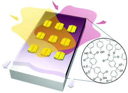
Herein, we report on the fabrication of large-area printed low-voltage organic thin film transistor arrays via minimal-solution bar-coating. We established the bar-coating of the chemically cross-linked polymer dielectric based on poly(4-vinylphenol) and 4,4′-(hexafluoroisopropylidene)diphthalic anhydride by investigating the effects of composition, reaction and printing conditions on film thickness, cross-linking efficacy, and dielectric properties. Subsequently, we elucidated various aspects of large-area (up to 4-inch wafer) bar-coated cross-linked polymeric dielectric prepared from minimal solution (∼100 μL, ∼1.2 μL cm−2) by addressing film uniformity, thickness control, capacitance variation, underlying step coverage, patternability, etc. The resultant polymeric dielectric exhibited good insulating properties as exemplified by a low leakage current density of ∼10−8 A cm−2 (at 1 MV cm−1) and a high areal capacitance of 42.6 nF cm−2. Finally, a highly-crystallized organic semiconductor layer based on 2,8-difluorinated 5,11-bis(triethylsilylethynyl)anthradithiophene was deposited on the bar-coated cross-linked polymeric dielectric via bar-coating, leading to the realization of printed low-voltage organic transistor arrays with minimum ink solution wasted.
