Efficient ternary organic photovoltaics with two polymer donors by minimizing energy loss†
Xiaoling
Ma
a,
Qiaoshi
An
a,
Olzhas A.
Ibraikulov
b,
Patrick
Lévêque
 b,
Thomas
Heiser
*b,
Nicolas
Leclerc
 *c,
Xiaoli
Zhang
d and
Fujun
Zhang
 *a
*a
aKey Laboratory of Luminescence and Optical Information, Ministry of Education, Beijing Jiaotong University, 100044, Beijing, China. E-mail: fjzhang@bjtu.edu.cn
bLaboratoire ICube, Université de Strasbourg, CNRS, UMR 7357, 23 rue du Loess, Strasbourg, 67037, France. E-mail: thomas.heiser@unistra.fr
cInstitut de Chimie et Procédés pour l'Energie, l'Environnement et la Santé (ICPEES), Université de Strasbourg, CNRS, UMR 7515, 25 rue Becquerel, 67087, Strasbourg, Cedex 02, France. E-mail: leclercn@unistra.fr
dState Centre for International Cooperation on Designer Low-Carbon & Environmental Materials, School of Materials Science and Engineering, Zhengzhou University, 450001, Zhengzhou, China
First published on 3rd December 2019
Abstract
Efficient ternary organic photovoltaics (OPVs) are fabricated with two polymer materials PF2 and J71 as donors and Y6 as the acceptor. The PF2 and J71 based binary OPVs exhibit 10.26% and 9.56% power conversion efficiency (PCE), respectively. Even with similar highest occupied molecular orbital (HOMO) energy levels of PF2 and J71, the J71 based binary OPVs show a relatively high open circuit voltage (VOC) of 0.86 V compared with 0.71 V for PF2 based binary OPVs. The VOCs of ternary OPVs monotonously increased with the increase of J71 content in donors, which should be mainly ascribed to the reduced energy loss according to the VOCs of two binary OPVs and the HOMO energy levels of two donors. The short circuit current density (JSC) and fill factor (FF) of ternary OPVs can also be simultaneously enhanced with the J71 content up to 30 wt% in donors, leading to 12.12% PCE of the optimized ternary OPVs with a JSC of 24.97 mA cm−2, a FF of 64.70% and a VOC of 0.75 V. Reducing energy loss by the ternary strategy is rarely reported in the literature, which should also be an efficient method to realize performance improvement of OPVs.
Introduction
Bulk heterojunction organic photovoltaics (OPVs) are promising for the realization of solar energy conversion with the advantages of light weight, flexibility, transparency and potential low cost.1–4 Great progress in single-junction OPVs has been achieved mainly due to the synthesis of nonfullerene acceptors and polymer donors exhibiting well-matched absorption spectra, energy levels and good morphological compatibility.5–8 Indeed, organic materials often possess a relatively narrow absorption spectral range with a full width at half maximum of about 100 nm, which should limit the photon harvesting range of one donor and one acceptor blend films. Adequate photon harvesting of active layers is very favorable for the fabrication of efficient OPVs. Ternary OPVs, including the blend of two donors/one acceptor or one donor/two acceptors with complementary absorption spectra, appear to be an increasingly promising approach.9–12 In addition to optimizing photon harvesting of active layers, the third component can be used to regulate the open circuit voltage (VOC) of ternary OPVs. It is well-recognized that the VOC of OPVs mainly depends on the energy level difference between the highest occupied molecular orbital (HOMO) energy level of the donor and the lowest unoccupied molecular orbital (LUMO) energy level of the acceptor, as well as energy loss (Eloss) in the photoelectric conversion process.13,14 The VOC of ternary OPVs may be improved by incorporating an acceptor with a higher LUMO energy level or a donor with a deeper HOMO energy level as the third component.15,16 Meanwhile, Eloss is inevitable in photoelectric conversion processes involving organic semiconductors, which should be influenced by two factors. One factor is the driving force for charge generation, which is defined as the offset between the bandgap of the donor/acceptor materials and the energy of the charge transfer state.5 A relatively small driving force is preferred to achieve fast and efficient charge separation. Another factor influencing Eloss is non-radiative recombination. Non-radiative recombination includes recombination through triplet states, structural defects and auger recombination, which constitute additional and detrimental loss channels.17 Reducing Eloss should be an effective method to realize VOC improvement. The VOC of ternary OPVs may be also improved by selecting an appropriate third component to decrease Eloss. Such a strategy is rarely reported in the literature.In this work, polymer donors (PF2 and J71) and the nonfullerene acceptor Y6 were employed to fabricate OPVs with the conventional structure ITO/PEDOT:PSS/active layer/PDIN/Al. Fig. 1a presents the schematic diagram of the device structure and the chemical structures of PF2, J71 and Y6. PF2 is a recently reported moderate bandgap (Egap) polymer that has been successfully used to fabricate efficient small size devices and large surface modules.18,19 It exhibits among other interesting properties, good charge transport properties and high structural stability under thermal treatment.20 J71 is a 2D conjugated wide Egap polymer that has been used in efficient OPVs by blending with nonfullerene acceptors.21 J71 exhibits a complementary absorption spectrum to the PF2 polymer. The new very low Egap Y6 molecule was selected as the nonfullerene acceptor, which recently led to record PCEs by blending with a polymer donor.22 The normalized absorption spectra of neat PF2, J71 and Y6 films are shown in Fig. 1b. The complementary absorption spectra of used materials may provide great potential in photon harvesting of ternary blend films as much as possible. The energy levels of used materials are depicted in Fig. 1c. The PF2 based binary OPVs exhibit a maximum power conversion efficiency (PCE) of 10.26% with a JSC of 23.17 mA cm−2, a VOC of 0.71 V and a FF of 62.35%. The J71 based binary OPVs exhibit a maximum PCE of 9.56% with a JSC of 22.97 mA cm−2, a VOC of 0.86 V and a FF of 48.42%. Although the HOMO energy level of J71 is slightly higher than that of PF2, the VOCs of binary OPVs are 0.86 V and 0.71 V for J71 and PF2 as donors, respectively, suggesting the relatively small Eloss in J71 based binary OPVs. The ternary OPVs achieve a maximum PCE of 12.12% with 30 wt% J71 in donors, benefiting from the synergistically improved JSC of 24.97 mA cm−2, FF of 64.70% and VOC of 0.75 V. Over 18% PCE improvement is achieved in the optimized ternary OPVs compared with the two binary OPVs, suggesting the great potential of the ternary strategy for performance improvement. This work provides an efficient pathway to improve the performance of OPVs by reducing Eloss with the ternary strategy.
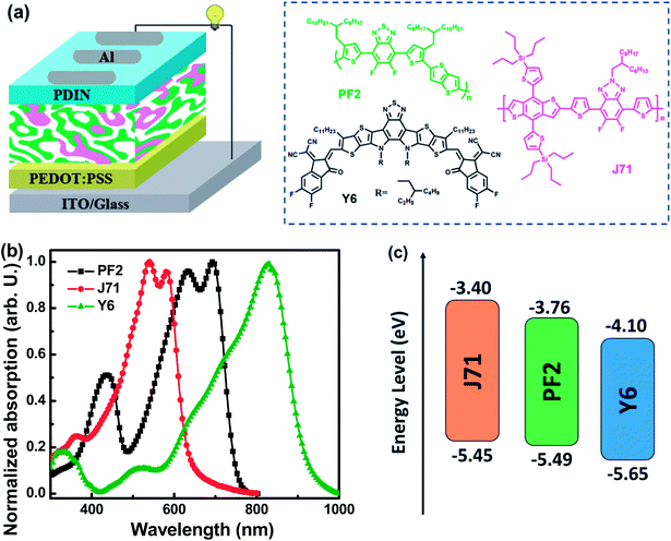 | ||
| Fig. 1 (a) Schematic diagram of the device structure and chemical structures of the used materials. (b) Normalized absorption spectra of neat films. (c) Energy levels of the used materials. | ||
Results and discussion
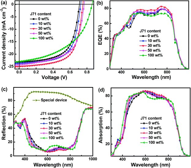
The current density versus voltage (J–V) characteristics of all OPVs were studied under standard AM 1.5G illumination of 100 mW cm−2, as shown in Fig. S1.† To clearly observe the effect of the J71 content on the performance of ternary OPVs, the J–V curves of typical OPVs are shown in Fig. 2a. The weight ratio of donors to acceptors is kept at 1![[thin space (1/6-em)]](https://www.rsc.org/images/entities/char_2009.gif) :
:![[thin space (1/6-em)]](https://www.rsc.org/images/entities/char_2009.gif) 1.5. The PF2:Y6 and J71:Y6 based OPVs exhibit PCEs of 10.26% and 9.56%, respectively. The binary OPVs exhibit similar JSCs (23.17 mA cm−2vs. 22.97 mA cm−2) and markedly different VOCs (0.71 V vs. 0.86 V) and FFs (62.35% vs. 48.42%) with PF2 and J71 as donors, respectively. The champion PCE achieves 12.12% for the optimized ternary OPVs with 30 wt% J71 in donors, resulting from the simultaneously increased JSC of 24.97 mA cm−2, VOC of 0.75 V and FF of 64.70%. The JSC and FF can be simultaneously improved when the J71 content in donors is up to 30 wt% and then decreased by incorporating more J71. The enhanced JSC and FF can be attributed to the improved photon harvesting and phase separation in the optimized ternary active layers. To better understand the dependence of FF variation of ternary OPVs on the J71 content in donors, the series resistance (RS) and shunt resistance (RSH) were calculated according to J–V curves of OPVs, as summarized in Table 1. The RSs of OPVs show a decreasing and then increasing trend with the increase of J71 content, and the RSHs of OPVs exhibit an opposite trend compared with RSs. A minimum RS of 3.6 Ω cm2 and a maximum RSH of 588 Ω cm2 were simultaneously obtained for the OPVs with 30 wt% J71 in donors, which are responsible for the highest FF of the optimized ternary OPVs. It is known that the VOC is mainly determined by the energy level difference between the HOMO of the donor and the LUMO of the acceptor, as well as the inevitable Eloss in the photoelectric conversion process. The HOMO energy levels of PF2 and J71 were measured by electrochemical cyclic voltammetry (CV),23,24 and the corresponding CV plots are illustrated in Fig. S2.† The HOMO energy levels of PF2 and J71 are −5.49 eV and −5.45 eV, respectively. The similar HOMO energy levels of two polymer donors should be conducive to hole transfer and transport in ternary active layers. The LUMO energy levels of PF2 and J71 can be evaluated according to the Egap of materials. The Egap of PF2 and J71 was calculated to be 1.73 eV and 2.05 eV according to the intersections between the normalized absorption and emission spectra of the corresponding neat films,25 as shown in Fig. S3.† The calculated LUMO energy levels are −3.76 eV and −3.40 eV for PF2 and J71, respectively. Eloss can be evaluated from the difference between the Egap of blend films and VOC of the corresponding OPVs.26–28 The Egap of blend films was estimated according to the intersection between the normalized absorption and emission spectra of the neat Y6 film,29 as shown in Fig. S4.† The Eloss of 0.68 eV for PF2 based binary OPVs is larger than 0.53 eV for J71 based binary OPVs. The Elosss of OPVs are gradually decreased from 0.68 eV to 0.53 eV with increasing J71 content in donors, which may be an important factor for PCE improvement of ternary OPVs. The key photovoltaic parameters and the corresponding Elosss of all OPVs are summarized in Table 1.
1.5. The PF2:Y6 and J71:Y6 based OPVs exhibit PCEs of 10.26% and 9.56%, respectively. The binary OPVs exhibit similar JSCs (23.17 mA cm−2vs. 22.97 mA cm−2) and markedly different VOCs (0.71 V vs. 0.86 V) and FFs (62.35% vs. 48.42%) with PF2 and J71 as donors, respectively. The champion PCE achieves 12.12% for the optimized ternary OPVs with 30 wt% J71 in donors, resulting from the simultaneously increased JSC of 24.97 mA cm−2, VOC of 0.75 V and FF of 64.70%. The JSC and FF can be simultaneously improved when the J71 content in donors is up to 30 wt% and then decreased by incorporating more J71. The enhanced JSC and FF can be attributed to the improved photon harvesting and phase separation in the optimized ternary active layers. To better understand the dependence of FF variation of ternary OPVs on the J71 content in donors, the series resistance (RS) and shunt resistance (RSH) were calculated according to J–V curves of OPVs, as summarized in Table 1. The RSs of OPVs show a decreasing and then increasing trend with the increase of J71 content, and the RSHs of OPVs exhibit an opposite trend compared with RSs. A minimum RS of 3.6 Ω cm2 and a maximum RSH of 588 Ω cm2 were simultaneously obtained for the OPVs with 30 wt% J71 in donors, which are responsible for the highest FF of the optimized ternary OPVs. It is known that the VOC is mainly determined by the energy level difference between the HOMO of the donor and the LUMO of the acceptor, as well as the inevitable Eloss in the photoelectric conversion process. The HOMO energy levels of PF2 and J71 were measured by electrochemical cyclic voltammetry (CV),23,24 and the corresponding CV plots are illustrated in Fig. S2.† The HOMO energy levels of PF2 and J71 are −5.49 eV and −5.45 eV, respectively. The similar HOMO energy levels of two polymer donors should be conducive to hole transfer and transport in ternary active layers. The LUMO energy levels of PF2 and J71 can be evaluated according to the Egap of materials. The Egap of PF2 and J71 was calculated to be 1.73 eV and 2.05 eV according to the intersections between the normalized absorption and emission spectra of the corresponding neat films,25 as shown in Fig. S3.† The calculated LUMO energy levels are −3.76 eV and −3.40 eV for PF2 and J71, respectively. Eloss can be evaluated from the difference between the Egap of blend films and VOC of the corresponding OPVs.26–28 The Egap of blend films was estimated according to the intersection between the normalized absorption and emission spectra of the neat Y6 film,29 as shown in Fig. S4.† The Eloss of 0.68 eV for PF2 based binary OPVs is larger than 0.53 eV for J71 based binary OPVs. The Elosss of OPVs are gradually decreased from 0.68 eV to 0.53 eV with increasing J71 content in donors, which may be an important factor for PCE improvement of ternary OPVs. The key photovoltaic parameters and the corresponding Elosss of all OPVs are summarized in Table 1.
| J71 content (wt%) | J SC (mA cm−2) | V OC (V) | FF (%) | PCE (Ave. ± Dev.) (%) | R S (Ω cm2) | R SH (Ω cm2) | E loss (eV) |
|---|---|---|---|---|---|---|---|
| a Average and deviation (Ave. ± Dev.) of PCEs were calculated with 10 cells prepared from different batch. | |||||||
| 0 | 23.17 | 0.71 | 62.35 | 10.26 (10.02 ± 0.32) | 5.2 | 524 | 0.68 |
| 10 | 23.72 | 0.73 | 63.37 | 10.97 (10.73 ± 0.24) | 5.0 | 532 | 0.66 |
| 20 | 24.31 | 0.74 | 64.43 | 11.59 (11.37 ± 0.22) | 4.5 | 559 | 0.65 |
| 30 | 24.97 | 0.75 | 64.70 | 12.12 (11.98 ± 0.19) | 3.6 | 588 | 0.64 |
| 40 | 24.86 | 0.76 | 63.15 | 11.93 (11.66 ± 0.17) | 3.9 | 523 | 0.63 |
| 50 | 24.28 | 0.77 | 60.27 | 11.27 (10.98 ± 0.23) | 4.2 | 410 | 0.62 |
| 70 | 23.63 | 0.78 | 54.02 | 9.96 (9.65 ± 0.19) | 5.4 | 268 | 0.61 |
| 100 | 22.97 | 0.86 | 48.42 | 9.56 (9.47 ± 0.20) | 7.6 | 234 | 0.53 |
The EQE spectra of typical OPVs were measured to further investigate the effect of J71 content on performance improvement, as shown in Fig. 2b. The EQE values of ternary OPVs are gradually enhanced in the wavelength range from 400 to 950 nm with increasing J71 content up to 30 wt% in donors, which may be mainly caused by well-balanced photon harvesting, exciton dissociation, charge transport and collection. To clarify the underlying reason of EQE enhancement by incorporating an appropriate amount of J71, photon harvesting of active layers in OPVs was investigated. The absorption spectra of active layers in OPVs can really reflect the contribution of the third component on photon harvesting of active layers by considering the interference effect between the incident light and the reflected light from the Al electrode.30,31 To obtain more accurate photon harvesting of active layers, specific devices were prepared with the same structure as OPVs to investigate the parasitic photon loss, and the only difference is using PMMA to replace the active layer. The parasitic photon loss of OPVs mainly originates from the glass/ITO substrate, interfacial layers and imperfect reflectivity of the Al electrode. The reflectance spectra of the special devices and OPVs were measured and are shown in Fig. 2c. The absorption spectra of active layers in OPVs can be obtained from the difference between the reflected spectra of OPVs and the reflected spectrum of the special device, as exhibited in Fig. 2d. The detailed calculation procedure is described in the ESI.† The photon harvesting of ternary active layers in the spectral range of 600–800 nm is slightly increased by incorporating J71 content up to 30 wt% in donors, which should be attributed to an interference effect in this spectral range. The photon harvesting of ternary active layers in the spectral range of 400–600 nm shows a gradually increasing trend with the increase of J71 content, which can be well explained according to the strong absorption ability of J71 in this spectral range.
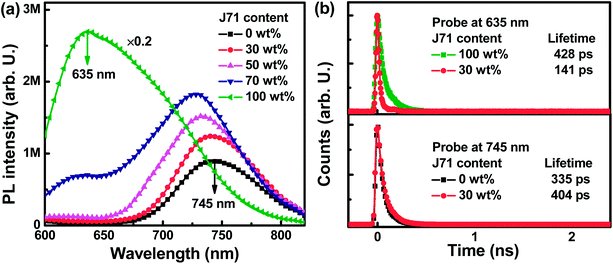
To investigate the dynamic process between PF2 and J71, photoluminescence (PL) spectra of neat and blend films were measured under 540 nm light excitation, as shown in Fig. 3a. A strong PL emission intensity can be observed from the neat J71 film with an emission peak at 635 nm. The neat PF2 film exhibits relatively weak PL emission intensity with an emission peak at 745 nm. The J71 emission intensity can be markedly quenched in blend PF2:J71 films. Meanwhile, the PF2 emission intensity in the blend films is monotonously increased with the increase of J71 content, indicating the existence of energy transfer from J71 to PF2. The energy transfer process can be well supported by the spectral overlap between the absorption spectrum of PF2 and the PL spectrum of J71, as shown in Fig. S5.† To further confirm energy transfer from J71 to PF2, time-resolved photoluminescence (TRPL) spectra of the neat and blend films were recorded as shown in Fig. 3b. The 635 nm emission lifetime is markedly decreased from 428 ps in the neat J71 film to 141 ps in blend films with 30 wt% J71 content. The 745 nm emission lifetime is 335 ps in the neat PF2 film and is increased to 404 ps for PF2:J71 blend films with 30 wt% J71 content. The occurrence of energy transfer from J71 to PF2 can be further confirmed from the decreased 635 nm emission lifetime and increased 745 nm emission lifetime in blend films.32–35 The energy transfer between J71 and PF2 should provide a new route to improve the exciton utilization efficiency in ternary OPVs. To investigate the potential charge transfer process between J71 and PF2, a series of cells were fabricated with PF2, J71 and PF2:J71 as the active layers. The J–V curves of the cells were measured under AM 1.5G illumination with a light intensity of 100 mW cm−2 and are shown in Fig. S6.† The JSC of PF2:J71 based cells is in between that of PF2 based and J71 based cells, suggesting negligible charge transfer or exciton dissociation at PF2 and J71 interfaces.
To gain more insight into the effect of incorporating J71 on the dynamic process of the ternary active layer, photogenerated current density dependence on effective voltage (Jph–Veff) curves of the optimized binary and ternary OPVs was studied as shown in Fig. 4a. All photogenerated charges will be adequately swept out and collected by electrodes under Veff > 2.5 V conditions, and the Jph comes into a saturated state defined as Jsat.36,37 The Jsat of 25.80 mA cm−2 in the optimized ternary OPVs is larger than 24.19 mA cm−2 in PF2:Y6 based OPVs, suggesting that more photons can be harvested in the optimized ternary active layers. The Jph/Jsat values under short circuit and maximal power output conditions represent the exciton dissociation efficiency (Pdiss) and charge collection efficiency (Pcoll), respectively.38 The corresponding Jph values are listed in Table S1.† The calculated Pdiss and Pcoll of the optimized ternary OPVs are 96.8% and 82.4%, which are much larger than 95.8% and 78.4% of PF2:Y6 based OPVs, respectively. The enhanced charge collection efficiency is in line with the relatively high 64.70% FF of the optimized ternary OPVs. To investigate the effect of the J71 content on charge transport in ternary active layers, charge mobility in active layers was investigated according to the space charge limited current (SCLC) model.39–42 Hole-only and electron-only devices were fabricated with the configuration ITO/PEDOT:PSS/active layer/MoO3/Ag and ITO/ZnO/active layer/PDIN/Al, respectively. The ln(Jd3/V2)–(V/d)0.5 curves of hole-only and electron-only devices are displayed in Fig. S7.† Both hole mobility (μh) and electron mobility (μe) in blend films show an increasing and then decreasing trend with the increase of J71 content in donors. To intuitively exhibit the charge mobility variation trend, the μh and μe dependence on the J71 content is shown in Fig. 4b. The μh and μe are increased to 8.10 × 10⁻⁴ cm2 V−1 s−1 and 1.15 × 10⁻⁴ cm2 V−1 s−1 in the optimized ternary active layers, respectively. The detailed μh, μe and μh/μe of the corresponding devices are shown in Table S2.† The charge transport in the optimized ternary active layers becomes more balanced according to the μh/μe values. The increased charge mobility and more balanced charge transport should result from the improved phase separation of active layers by incorporating an appropriate amount of J71.
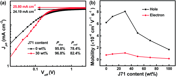 | ||
| Fig. 4 (a) Jph–Veff curves of the optimized binary and ternary OPVs. (b) Dependence of hole and electron mobility in blend films on the J71 content in donors. | ||
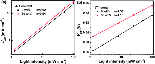
To figure out the charge recombination process in active layers, the J–V curves of the optimized binary and ternary OPVs were measured under different incident light intensities (I), as shown in Fig. S8.† According to the J–V curves under different I values, the dependence of JSC and VOC of the optimized binary and ternary OPV on I is presented in Fig. 5. The charge recombination can be evaluated according to the JSC dependence on I obeying the power law equation JSC ∝ Is, where s is the exponential factor and the slope of the fitted line.43–45 The fitted ‘s’ values are 0.92 and 0.94 for PF2:Y6 based and optimized ternary OPVs, respectively. The fitted ‘s’ value for the optimized ternary OPVs is closer to 1, indicating that the bimolecular recombination in active layers can be slightly restrained with appropriate J71 incorporation. The charge recombination can be assessed according to VOC ∝ n(KT/q)ln(I), in which K, T, and q represent the Boltzmann constant, temperature in Kelvin, and elementary charge, respectively.46–48 The fitted ‘n’ values are 1.31 and 1.15 for PF2 based binary OPVs and the optimized ternary OPVs, respectively. The smaller ‘n’ value of 1.15 suggests that trap-assisted recombination of active layers can be effectively reduced with appropriate J71 incorporation. The bimolecular and trap-assisted recombination can be synchronously suppressed in the optimized ternary OPVs, resulting in the relatively high FF of the optimized ternary OPVs.
The surface morphology of blend films with different J71 contents was characterized by atomic force microscopy (AFM). The AFM height images and phase images of blend films are shown in Fig. 6a and b, respectively. The root-mean-square (RMS) roughness values of blend films are slightly decreased from 2.14 nm to 1.79 nm or 1.77 nm with the J71 content in donors increasing to 30 wt% or 50 wt%, respectively. The slight roughness variation suggests the good compatibility among the used materials. Fibrillar and grain-like structures can be clearly observed from the phase images of PF2:Y6 and J71:Y6 blend films, respectively. As observed from the AFM phase images of ternary blend films, the length of the fibrillar structure is slightly increased along with the increase of J71 content in donors. The surface morphology of blend films can be adjusted by incorporating J71 as the third component. The bulk morphology of blend films was characterized via transmission electron microscopy (TEM), as shown in Fig. 6c. The bright and dark regions can be assigned to the donor-rich and acceptor-rich domains, respectively. Markedly different phase separation degrees can be observed from the TEM images of two binary blend films. The fibrillar structure with a relatively small phase separation degree can be observed from the TEM images of PF2:Y6 based blend films. The island-like structure with a large phase separation degree can be observed from the TEM images of J71:Y6 based blend films, which could hinder exciton dissociation due to limited donor/acceptor interfaces. As seen from the TEM images of ternary blend films, the donor and acceptor aggregated structure and phase separation degree are apparently varied depending on the J71 content. Well-optimized nanoscale phase separation should be present for sufficient exciton dissociation and efficient charge transport in ternary active layers by incorporating an appropriate amount of J71.
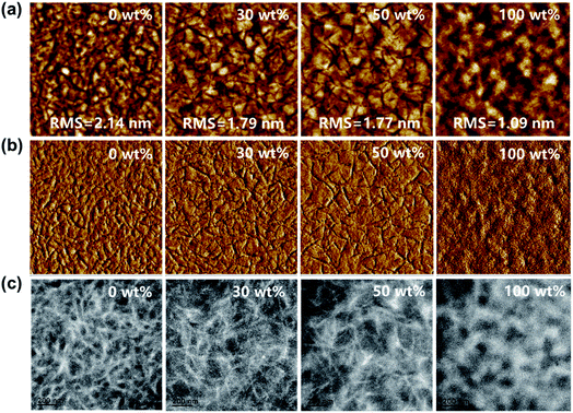 | ||
| Fig. 6 (a) AFM height images, (b) AFM phase images and (c) TEM images of blend films with different J71 contents in donors. | ||
Conclusions
In summary, a series of binary and ternary OPVs were successfully constructed with Y6 as the acceptor and PF2 and J71 as donors. The PCEs of PF2 and J71 based binary OPVs reach 10.26% and 9.56%, respectively. Although the J71 based binary OPVs exhibit a slightly low PCE, the VOC of 0.86 V is much larger than 0.71 V of PF2 based binary OPVs, suggesting relatively small Eloss in J71 based binary OPVs. The PCE of ternary OPVs is increased to 12.12% by incorporating 30 wt% J71 into donors, with a simultaneously improved JSC of 24.97 mA cm−2, FF of 64.70% and VOC of 0.75 V. Over 18% PCE improvement can be achieved by employing the ternary strategy in comparison with two binary OPVs. The complementary absorption spectra of PF2 and J71 can maximize photon harvesting of ternary active layers with appropriate J71 incorporation, leading to the improved JSCs of ternary OPVs. The phase separation can be further optimized in the ternary active layers for efficient exciton dissociation and charge transport. Meanwhile, the Elosss of OPVs can be gradually decreased by increasing the J71 content in donors. This work may provide a new insight for realizing performance improvement of OPVs by minimizing Eloss with ternary strategy.Conflicts of interest
There are no conflicts to declare.Acknowledgements
This work was supported by the National Natural Science Foundation of China (61675017, 61975006) and the Beijing Natural Science Foundation (4192049).Notes and references
- J. Hou, O. Inganäs, R. H. Friend and F. Gao, Nat. Mater., 2018, 17, 119 CrossRef CAS PubMed.
- W. Gao, M. Zhang, T. Liu, R. Ming, Q. An, K. Wu, D. Xie, Z. Luo, C. Zhong, F. Liu, F. Zhang, H. Yan and C. Yang, Adv. Mater., 2018, 30, 1800052 CrossRef PubMed.
- H. Kang, G. Kim, J. Kim, S. Kwon, H. Kim and K. Lee, Adv. Mater., 2016, 28, 7821 CrossRef CAS PubMed.
- Z. Hu, Z. Wang, Q. An and F. Zhang, Sci. Bull., 2019 DOI:10.1016/j.scib.2019.09.016.
- J. Liu, S. Chen, D. Qian, B. Gautam, G. Yang, J. Zhao, J. Bergqvist, F. Zhang, W. Ma and H. Ade, Nat. Energy, 2016, 1, 16089 CrossRef CAS.
- C. Yan, S. Barlow, Z. Wang, H. Yan, A. K.-Y. Jen, S. R. Marder and X. Zhan, Nat. Rev. Mater., 2018, 3, 18003 CrossRef CAS.
- F. Huang, Z. Bo, Y. Geng, X. Wang, L. Wang, Y. Ma, J. Hou, W. Hu, J. Pei, H. Dong, S. Wang, Z. Li, Z. Shuai, Y. Li and Y. Cao, Acta Polym. Sin., 2019, 50, 988 Search PubMed.
- G. Zhang, J. Zhao, P. C. Chow, K. Jiang, J. Zhang, Z. Zhu, J. Zhang, F. Huang and H. Yan, Chem. Rev., 2018, 118, 3447 CrossRef CAS PubMed.
- X. Du, X. Lu, J. Zhao, Y. Zhang, X. Li, H. Lin, C. Zheng and S. Tao, Adv. Funct. Mater., 2019, 29, 1902078 CrossRef.
- Z. Hu, F. Zhang, Q. An, M. Zhang, X. Ma, J. Wang, J. Zhang and J. Wang, ACS Energy Lett., 2018, 3, 555 CrossRef CAS.
- W. Xu and F. Gao, Mater. Horiz., 2018, 5, 206 RSC.
- J. Gao, J. Wang, Q. An, X. Ma, Z. Hu, C. Xu, X. Zhang and F. Zhang, Sci. China: Chem., 2019 DOI:10.1007/s11426-019-9634-5.
- N. K. Elumalai and A. Uddin, Energy Environ. Sci., 2016, 9, 391 RSC.
- C. Xu, J. Wang, Q. An, X. Ma, Z. Hu, J. Gao, J. Zhang and F. Zhang, Nano Energy, 2019, 66, 104119 CrossRef CAS.
- T. Yan, W. Song, J. Huang, R. Peng, L. Huang and Z. Ge, Adv. Mater., 2019, 31, 1902210 CrossRef PubMed.
- Y. Chang, T.-K. Lau, M.-A. Pan, X. Lu, H. Yan and C. Zhan, Mater. Horiz., 2019, 6, 2094 RSC.
- D. Qian, Z. Zheng, H. Yao, W. Tress, T. R. Hopper, S. Chen, S. Li, J. Liu, S. Chen and J. Zhang, Nat. Mater., 2018, 17, 703 CrossRef CAS PubMed.
- O. A. Ibraikulov, C. Ngov, P. Chávez, I. Bulut, B. Heinrich, O. Boyron, K. L. Gerasimov, D. A. Ivanov, S. Swaraj and S. Méry, J. Mater. Chem. A, 2018, 6, 12038 RSC.
- O. A. Ibraikulov, J. Wang, N. Kamatham, B. Heinrich, S. Méry, M. Kohlstädt, U. Würfel, S. Ferry, N. Leclerc, T. Heiser and P. Lévêque, Sol. RRL, 2019, 3, 1900273 CrossRef CAS.
- Y. Zhong, L. Biniek, N. Leclerc, S. Ferry and M. Brinkmann, Macromolecules, 2018, 51, 4238 CrossRef CAS.
- H. Bin, L. Gao, Z.-G. Zhang, Y. Yang, Y. Zhang, C. Zhang, S. Chen, L. Xue, C. Yang and M. Xiao, Nat. Commun., 2016, 7, 13651 CrossRef CAS PubMed.
- J. Yuan, Y. Zhang, L. Zhou, G. Zhang, H.-L. Yip, T.-K. Lau, X. Lu, C. Zhu, H. Peng and P. A. Johnson, Joule, 2019, 3, 1140 CrossRef CAS.
- L. Zhong, L. Gao, H. Bin, Q. Hu, Z. G. Zhang, F. Liu, T. P. Russell, Z. Zhang and Y. Li, Adv. Energy Mater., 2017, 7, 1602215 CrossRef.
- M. Zhang, Z. Xiao, W. Gao, Q. Liu, K. Jin, W. Wang, Y. Mi, Q. An, X. Ma and X. Liu, Adv. Energy Mater., 2018, 8, 1801968 CrossRef.
- Y. Wang, D. Qian, Y. Cui, H. Zhang, J. Hou, K. Vandewal, T. Kirchartz and F. Gao, Adv. Energy Mater., 2018, 8, 1801352 CrossRef.
- S. M. Menke, N. A. Ran, G. C. Bazan and R. H. Friend, Joule, 2018, 2, 25 CrossRef CAS.
- W. Li, K. H. Hendriks, A. Furlan, M. M. Wienk and R. A. Janssen, J. Am. Chem. Soc., 2015, 137, 2231 CrossRef CAS PubMed.
- T. Heumueller, T. M. Burke, W. R. Mateker, I. T. Sachs-Quintana, K. Vandewal, C. J. Brabec and M. D. McGehee, Adv. Energy Mater., 2015, 5, 1500111 CrossRef.
- R. Yu, H. Yao, Y. Cui, L. Hong, C. He and J. Hou, Adv. Mater., 2019, 31, 1902302 CrossRef PubMed.
- W. Wang, F. Zhang, M. Du, L. Li, M. Zhang, K. Wang, Y. Wang, B. Hu, Y. Fang and J. Huang, Nano Lett., 2017, 17, 1995 CrossRef CAS PubMed.
- J. Miao and F. Zhang, Laser Photonics Rev., 2019, 13, 1800204 Search PubMed.
- L. Lu, W. Chen, T. Xu and L. Yu, Nat. Commun., 2015, 6, 7327 CrossRef CAS PubMed.
- X. Xu, Z. Bi, W. Ma, Z. Wang, W. C. Choy, W. Wu, G. Zhang, Y. Li and Q. Peng, Adv. Mater., 2017, 29, 1704271 CrossRef PubMed.
- B. Kan, Y. Q. Q. Yi, X. Wan, H. Feng, X. Ke, Y. Wang, C. Li and Y. Chen, Adv. Energy Mater., 2018, 8, 1800424 CrossRef.
- Q. An, J. Wang and F. Zhang, Nano Energy, 2019, 60, 768 CrossRef CAS.
- Z. Li, J. D. Lin, H. Phan, A. Sharenko, C. M. Proctor, P. Zalar, Z. Chen, A. Facchetti and T. Q. Nguyen, Adv. Funct. Mater., 2014, 24, 6989 CrossRef CAS.
- X. Ma, M. Luo, W. Gao, J. Yuan, Q. An, M. Zhang, Z. Hu, J. Gao, J. Wang and Y. Zou, J. Mater. Chem. A, 2019, 7, 7843 RSC.
- T. Liu, Z. Luo, Q. Fan, G. Zhang, L. Zhang, W. Gao, X. Guo, W. Ma, M. Zhang and C. Yang, Energy Environ. Sci., 2018, 11, 3275 RSC.
- X. Du, J. Zhao, H. Zhang, X. Lu, L. Zhou, Z. Chen, H. Lin, C. Zheng and S. Tao, J. Mater. Chem. A, 2019, 7, 20139 RSC.
- M. Zhang, F. Zhang, Q. An, Q. Sun, W. Wang, X. Ma, J. Zhang and W. Tang, J. Mater. Chem. A, 2017, 5, 3589 RSC.
- Y. Xie, F. Yang, Y. Li, M. A. Uddin, P. Bi, B. Fan, Y. Cai, X. Hao, H. Y. Woo and W. Li, Adv. Mater., 2018, 30, 1803045 CrossRef PubMed.
- K. Jiang, Q. Wei, J. Y. L. Lai, Z. Peng, H. K. Kim, J. Yuan, L. Ye, H. Ade, Y. Zou and H. Yan, Joule, 2019 DOI:10.1016/j.joule.2019.09.010.
- Q. An, F. Zhang, W. Gao, Q. Sun, M. Zhang, C. Yang and J. Zhang, Nano Energy, 2018, 45, 177 CrossRef CAS.
- X. Du, S. Tao, L. Li, W. Wang, C. Zheng, H. Lin, X. Zhang and X. Zhang, Sol. RRL, 2018, 2, 1800038 CrossRef.
- C. Wang, X. Xu, W. Zhang, S. B. Dkhil, X. Meng, X. Liu, O. Margeat, A. Yartsev, W. Ma and J. Ackermann, Nano Energy, 2017, 37, 24 CrossRef CAS.
- R. Street, S. Cowan and A. Heeger, Phys. Rev. B: Condens. Matter Mater. Phys., 2010, 82, 121301 CrossRef.
- M. Zhang, F. Zhang, Q. An, Q. Sun, W. Wang, J. Zhang and W. Tang, Nano Energy, 2016, 22, 241 CrossRef CAS.
- W. Su, Q. Fan, X. Guo, X. Meng, Z. Bi, W. Ma, M. Zhang and Y. Li, Nano Energy, 2017, 38, 510 CrossRef CAS.
Footnote |
| † Electronic supplementary information (ESI) available: Experimental details, J–V curves, CV plots, absorption and emission spectra, Jph values, ln(Jd3/V2)–(V/d)0.5 curves, and hole and electron mobility. See DOI: 10.1039/c9ta12025d |
| This journal is © The Royal Society of Chemistry 2020 |

