
Reliability issues of amorphous oxide semiconductor-based thin film transistors
Yuxuan
Shen†
a,
Meng
Zhang†
ab,
Siyuan
He
a,
Le
Bian
a,
Jiaxin
Liu
a,
Zhengyu
Chen
a,
Shuangmei
Xue
ab,
Ye
Zhou
 a and
Yan
Yan
*ab
a and
Yan
Yan
*ab
aState Key Laboratory of Radio Frequency Heterogeneous Integration (Shenzhen University), Shenzhen 518060, China. E-mail: yanyan@szu.edu.cn
bCollege of Electronics and Information Engineering (Shenzhen University), Shenzhen 518060, China
First published on 15th August 2024
Abstract
Amorphous oxide semiconductors (AOSs) are non-crystalline compounds composed of metal elements and oxygen elements, possessing distinctive electrical properties. Even in their amorphous state, these materials exhibit favourable carrier transport paths and demonstrate high mobilities. Thin-film transistors (TFTs), as the core devices in active matrix drive systems, have found commercial success in active matrix liquid crystal displays and active matrix organic light-emitting diode displays. Among the choices of active layer materials for TFTs, AOSs have emerged as a potent alternative to traditional Si-based semiconductors, offering irreplaceable advantages in large-area high-definition flat-panel displays. Currently, the reliability concerns regarding AOS TFTs have garnered increasing attention, yet reports on this topic are scattered. Therefore, a comprehensive overview of the aspects is necessary to facilitate further progress in this field. With next-generation display technologies demanding large-area, high-resolution, and high-refresh-rate displays, alongside the challenges presented by future flexible display technologies in coping with complex working scenarios such as bending and stretching, the significance of this research is unmistakable. Critical directions for future research are proposed in an updated, top-tier roadmap to galvanize progress towards AOS TFTs within the community.
 Yan Yan | Yan Yan received his BS and MS degrees from Soochow University in China in 2009 and 2012, respectively, and received his PhD degree from City University of Hong Kong in 2016. He has joined the College of Electronics and Information Engineering at Shenzhen University in 2016, and currently serves as an associate professor. His research interests are in the areas of semiconductor devices and integration, focusing on thin film transistors, optoelectronic sensing, and their applications. He has published more than 80 SCI papers in journals such as IEEE Electron Device Letters, IEEE Transactions on Electron Devices and Small. |
1. Introduction
The advancement and application of semiconductor materials have had a huge impact on modern technology, economy, and social development, thereby promoting the progress of human society. Presently, Si and its derivatives occupy a prominent position among the most commonly utilized semiconductors, attributed to their natural abundance and well-established industrial processes. Over the past few decades, profound exploration in materials science and electronics has led to remarkable advancements in the theoretical understanding and practical applications of semiconductor materials. Consequently, there has been a continuous emergence of novel semiconductor materials and processing techniques.Oxide semiconductors are a category of oxide materials with semiconductor properties, mainly composed of metal oxides and elemental oxides. Metal oxide semiconductors typically show a wide bandgap width (2–3 eV) and exhibit insulating properties at low carrier concentrations at room temperature when in an ideal stoichiometric ratio.1–3 However, most metal oxide semiconductors can become semiconductors when doped with impurities. In order to explain the main semiconductor properties of oxides, especially the carrier transport phenomena, the initial research on covalent semiconductors such as Ge and Si was used to establish concepts and supplemented with new concepts related to ionic bonding. However, these concepts only apply to wide bandgap oxide semiconductors with high carrier mobility (μ). The latest research shows that heavy metals such as In, Ga, and Zn, and post transition metal cations have special electronic structures.4–6 Even in the amorphous state of oxide semiconductors, they still have good carrier transport pathways and exhibit high Hall μ similar to those of the corresponding crystal materials.7 In recent years, oxide semiconductors have been widely used, and their main structural form is oxide semiconductor thin films. Techniques such as sputtering,8,9 spin-coating,10 molecular beam epitaxy (MBE),11–13 atomic layer deposition (ALD),14–17 metal–organic chemical vapor deposition (MOCVD),18,19 and laser pulse deposition (LPD) can all be used to prepare high-quality oxide films.20 Due to the transparency of metal oxide semiconductors with a bandgap above 3.1 eV in the visible light region and their excellent optical, electrical, ferroelectric, and piezoelectric properties, transparent metal oxides have been widely used in fields such as solar cells, liquid crystal displays, gas sensors, and transparent electromagnetic shielding. However, the above-mentioned transparent oxide semiconductors are only used as passive electrical or optical layers.21–23 As functional materials for active devices, they are widely used in thin-film transistors (TFTs),24–27 light-emitting diodes (LEDs),28–30 and lasers.31
With the popularization of mobile internet and smart phones, flat-panel displays have become an indispensable part of people's daily life, work and entertainment. High-definition displays are one of the development trends of flat panel displays, and active-matrix drive technology is the key technology to achieve it. According to the type of driving devices, applications of active matrix driving systems mainly include active-matrix liquid-crystal displays (AMLCDs) and active matrix organic light emitting diode (AMOLED) displays.32 In the AMLCDs, a switch TFT is introduced in each pixel. In the AMOLED displays, since OLEDs are current-driven optoelectronic devices, in addition to a switch TFT, a driving TFT is also added to each AMOLED pixel to provide a stable driving current for the OLEDs.
At present, the semiconductor materials used in commercially applied TFTs are mainly amorphous silicon (a-Si) and low-temperature polycrystalline silicon (P-Si). Among them, a-Si TFTs are mainly used in low-end large-area display imaging due to the limitation of low μ around 0.5–1 cm2 V−1 s−1.33 Low-temperature P-Si TFTs have excellent μ (30–200 cm2 V−1 s−1), but are limited by complex production processes, high cost, poor film consistency, and bad mechanical stress tolerance.34,35 Currently, they are primarily utilized in active-matrix drive circuits for small-size displays with high definition. In the past twenty years, amorphous oxide semiconductors (AOSs) have become a powerful alternative to traditional Si-based semiconductors because of their good industrial production compatibility, high μ (10–120 cm2 V−1 s−1), excellent film uniformity, ease of large-area deposition, and good mechanical stress tolerance.7,36–38
The reliability of devices is crucial to ensuring the quality and performance of electronic products. It not only enhances the stability of products and reduces failure rates but also extends their lifespan, thereby improving user satisfaction. In practical circuit operations, the reliability of switching TFTs directly affects pixel activation, while fluctuations in the electrical signals of driving TFTs can lead to significant changes in OLED luminance.39,40 Thus, it is evident that highly reliable TFTs constitute a prerequisite for achieving stable flat-panel displays. TFTs are prone to various reliability challenges and underlying failure mechanisms, necessitating a comprehensive overview of the subject for further advancements in this domain. At present, the majority of the research on the reliability of AOS TFTs focuses on bias stress stability testing. In addition, the effects of lighting, temperature, atmosphere, AC stress, bending stress, and electrostatic discharge on reliability have gradually become research hotspots. Despite the growing interest in the reliability issues of AOS-based TFTs, the pertinent reports are dispersed across various literature sources. Therefore, the objective of this paper is to offer a consolidated overview, summarizing the findings of existing literature on this topic, and to delve into its current status and anticipated future research directions.
2. Materials
2.1. AOS materials
Oxide semiconductors are a class of oxide materials with semiconductor properties, and oxide semiconductor films are the main morphological structure used in applications. The oxide semiconductors used in TFTs are mainly metal oxides. Among them, metal oxide semiconductors (InO, ZnO, SnO2, etc.) with a bandgap above 3.1 eV show high transmittance in the visible light region, so they are also called transparent oxide semiconductors. Research on oxide semiconductors can be traced back to the early 20th century, but people's understanding of the basic properties of oxide semiconductors is far less than that of traditional semiconductor materials such as Ge and Si. There are many reasons for this. First, the preparation of perfect oxide semiconductor single crystals is extremely challenging, and obtaining relevant data/information is not entirely reliable. Second, compared with the structures of Ge, Si, and III–V compound semiconductors, those of oxide semiconductors are more complex. In addition, the existence of ionic bonds in oxide molecules causes the carrier transport mechanism to be different from that for traditional semiconductors.At the beginning of the 20th century, researchers discovered that CdO is a good n-type semiconductor.41 Foreign element-doped and other CdO-related compounds, such as CdSnO3, Cd2SnO4, and CdIn2O4, all show good electrical properties and μ.42,43 However, due to the toxicity of Cd,44 the marketization of this type of material has become less realistic. Subsequently, binary oxide semiconductors such as In2O3, SnO2, and ZnO became research hotspots.45–47 In 1968, Boesen et al. published an article on metallic lithium-doped single-crystalline ZnO TFTs,48 achieving a high Hall μ of 220 cm2 V−1 s−1, but the single crystal preparation temperature was too high to be compatible with the TFTs’ fabrication for flat panel displays. In 2003, Hofmann and Carcia's research groups reported polycrystalline ZnO TFTs prepared at room temperature.21,49 TFTs exhibited a μ value of 2.5 cm2 V−1 s−1, showing great application potential. However, the deposited ZnO films usually exhibited a polycrystalline structure, and the randomness of grain boundary distribution led to unsatisfactory large-area uniformity of the films. At the same time, defects at the grain boundaries, such as oxygen vacancies (VO) and zinc gaps, result in high carrier concentration in the film at room temperature and poor reliability under various stress conditions of electricity, light, and thermal stress, leading to a severe shift of threshold voltage (VTH).50–52
AOS materials can avoid grain boundary problems, enabling the attainment of large-area, homogenous, and low-temperature film deposition. Consequently, the advancement of high-performance and high-reliability AOS TFTs has emerged as a prominent focal point in contemporary research. AOS materials can be formed by mixing multiple materials with different crystal structures. For instance, IZO composed of In2O3 and ZnO with diverse crystal structures can exhibit an amorphous phase. Amorphous IZO (a-IZO) shows high μ and good thermal stability,53 and its carrier concentration can be controlled by adjusting the cation ratio in the film during the preparation process. As shown in Fig. 1, the high μ of AOS originates from its unique electron orbital structure. Heavy metals such as In, Ga, and Zn and post-transition metal element cations have an (n − 1)d10ns0 (n is greater than or equal to 4) electronic structure, and their carrier transport paths are composed of isotropic spatial metal ns orbitals. Direct overlap can occur between adjacent metal s orbitals, and s orbitals have spherical symmetry, making these types of AOS materials insensitive to structural deformation and maintain high μ even in the amorphous state.7,54
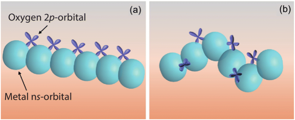 | ||
| Fig. 1 Carrier transport paths of (a) crystalline and (b) amorphous post-transition-metal oxide semiconductors. Reproduced with permission.7 Copyright 2024, Springer Nature. | ||
Due to the large number of active VO inside IZO, it is difficult to reduce the carrier concentration to a lower value (<1016 cm−3), which leads to a higher off current and a smaller on/off ratio of TFTs.55 In order to suppress the excessive VO inside the IZO film, some metal elements such as Ga, Hf, and Al can be doped into it, which can form a tight combination with oxygen, thereby effectively reducing the carrier concentration and decreasing the off current.56,57 In 2003, Nomura et al. prepared single crystalline IGZO TFTs with μ of up to 80 cm2 V−1 s−1 and an on/off ratio of ∼106. However, the temperature of the IGZO fabrication process was above 1000 °C,58 which is incompatible with glass and plastic substrates. Based on this, in 2004, they successfully deposited amorphous IGZO (a-IGZO) at room temperature, enabling the production of high-performance TFTs with an electron μ of approximately 10 cm2 V−1 s−1, which significantly promoted the application of AOSs in flat panel displays.7 Currently, the crystal structures of IGZO include single crystalline, polycrystalline, c-axis aligned crystalline (CAAC), nanocrystalline, and amorphous structures. Among them, single crystalline and polycrystalline IGZO need to be formed at high temperatures, and the associated equipment and fabrication processes are complex, hence unsuitable for large-scale industrial production and incompatible with glass and plastic substrates. However, CAAC, nanocrystalline, and amorphous IGZO show the advantages of low manufacturing cost, good reliability, high electron μ, and outstanding large-area uniformity, and are well-suited for large-scale industrialization. Presently, a-IGZO TFT and CAAC-IGZO TFT technologies have been commercially applied in TFT-LCDs and TFT-AMOLEDs, exhibiting irreplaceable advantages in large-scale display products.
Fig. 2 illustrates the effect of elemental composition on the electron transport properties of the In2O3–Ga2O3–ZnO system. As the In content increases, the Hall μ of the film grows, but the excessive doping of In increases the number of free carriers in the channel, causing a high off current of TFTs. Zn ions have a stable tetrahedral structure and can maintain the amorphous state of the material. The chemical bond formed between Ga ions and O ions is stronger than that of Zn and In ions with O ions. Therefore, the addition of Ga can inhibit the formation of VO and plays a role in controlling the carrier concentration. Nevertheless, since VO acts as shallow-donor impurities within the a-IGZO film, adding excessive Ga will greatly reduce the carrier concentration, leading to a deterioration of μ. Thus, adding an appropriate amount of inhibitory ions is crucial for obtaining stable AOS materials and TFTs.50
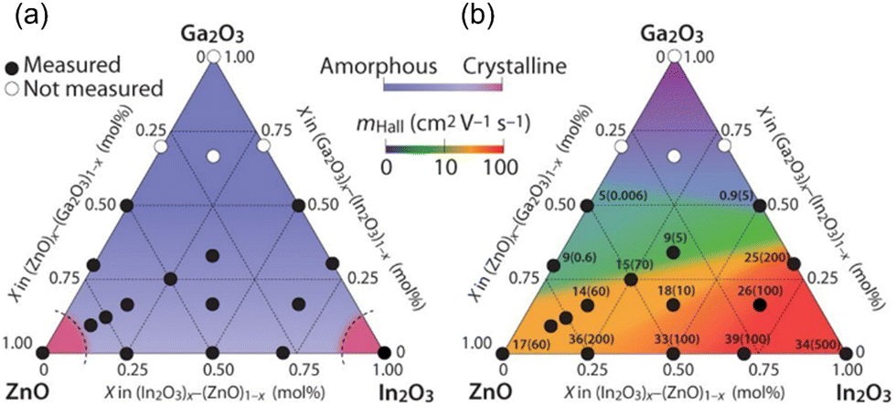 | ||
| Fig. 2 (a) Crystal morphology distribution and (b) electron transport properties in an In2O3–Ga2O3–ZnO system. In (b), the values outside parentheses denote the electron Hall μ (cm2 V−1 s−1) density, and the values inside parentheses denote the electron concentration (× 1018 cm−3). Reproduced with permission.51 Copyright 2024, NPG Asia Materials. | ||
From the above discussion, it can be found that due to the bidirectional effects of Ga, μ of a-IGZO TFTs can also be limited to ensure the electrical reliability of the device. With the development of future high-definition display technology, there are higher requirements for achieving high μ and stability of TFTs. Hence, new multi-element AOSs have become a research hotspot. In 2011, Fukumoto et al. proposed TFTs using amorphous ITZO (a-ITZO) as the active layer,59 which showed a very high μ (30.9 cm2 V−1 s−1) and exhibited excellent electrical stability after bias temperature stress application. In 2014, Song et al. reported a-ITZO TFTs with μ as high as 52 cm2 V−1 s−1, and the off current did not deteriorate.60 The high μ of a-ITZO stems from the fact that the bottom of the a-ITZO conduction band is mainly composed of In 5s and Sn 5s orbitals, which have strong divergence and high symmetry. At the same time, because Sn can replace Ga atoms to suppress the formation of oxygen-related defects within the film, it can effectively improve the stability of TFTs,61 and since Sn is easier to obtain, it can also reduce the fabrication cost of a-ITZO TFTs. In addition, a-ITZO shows a larger bandgap and higher transparency in the visible range. These advantages make a-ITZO TFTs particularly suitable for displays and various optoelectronic applications. In addition to Sn, Tungsten (W) is also a good alternative dopant to Ga and its cost is lower. W has a strong binding ability with O, and can inhibit the formation of VO and is an excellent carrier inhibitor. Therefore, amorphous IWZO (a-IWZO) is also very suitable as an active layer material for TFTs.62–64
It is noteworthy to mention that the oxide semiconductors discussed in this article primarily exhibit n-type characteristics. Due to the limited μ and difficulty of the preparation of p-type oxide semiconductor materials represented by CuO, SnO, and NiO, their development is slow, and the reported research on these materials is scarce and lacks a comprehensive, systematic approach. Therefore, their discussion will not be included in the scope of this review.
2.2. Thin film fabrication techniques and regulation
There exist numerous techniques for depositing AOS thin films, with the principal methods encompassing sputtering, solution-based processes, and ALD. Additionally, PECVD and PLD have also been employed as viable methods for depositing AOS thin films.54 In the following text, we shall delve into several of the prevailing deposition techniques.Sputtering refers to the technique of using high-energy particles to bombard the target material in a vacuum environment, causing the target atoms or molecules to shoot out from the surface and deposit onto a thin film on a substrate. Sputtering is the most commonly used method for the preparation of AOS films.65 The films prepared by sputtering have good density and uniformity, are suitable for large-area preparation with lost cost, and can also produce high-performance AOS TFTs (10–60 cm2 V−1 s−1).66–69 Taking IGZO as an example, IGZO TFTs based on sputtering have achieved an μ of 55.3 cm2 V−1 s−1.70 By controlling the deposition conditions (sputtering power, deposition time, etc.), the properties of the films can be manipulated. Additionally, the deposition of multi-component AOS materials (such as IGZO and ITZO) can be achieved by altering the target ratio and composition. However, sputtering also possesses certain disadvantages. For instance, the deposition of the film necessitates a high vacuum environment, which can be challenging to maintain. Furthermore, the bombardment of high-energy particles during the sputtering process may potentially lead to thermal damage to the films, thereby compromising their quality and performance.
The solution method refers to coating a substrate with a metal precursor dissolved in a solvent by spin coating, inkjet printing, etc., and then through thermal annealing to form films. The process is simple and does not require a high vacuum environment and complex equipment. Furthermore, the precursor solution is relatively inexpensive, which can reduce the cost of device preparation. The solution method also boasts advantages like quick preparation and large area coverage.71 By adjusting the molar ratio of precursor solution components and annealing temperature, the transport characteristics of AOS films can be regulated, and thus the performance of TFTs can be adjusted. According to early studies, the solution method was often limited by lower film quality and correspondingly low μ. For instance, conventional solution-processed IGZO typically exhibits μ within 20 cm2 V−1 s−1.72–79 More notably, the solution method can be used to easily achieve AOS films with a bi-layer structure. The ITZO/IGZO TFTs have been reported to show a μ of 51 cm2 V−1 s−1. Ultra-violet (UV) irradiation is also a common technique for treating solution-processed AOS films. Both UV and deep UV (DUV) have high energy, which can provide an annealing effect on AOS films. They have been reported to break unstable M–H and M–M bonds within AOS and form stable M–O bonds. UV/DUV-treated AOS TFTs have exhibited μ more than 10 cm2 V−1 s−1.80–84 By Sn doping, solution-processed IGZO TFTs can show a μ of 65 cm2 V−1 s−1.85
ALD refers to the deposition of thin films layer by layer in the form of single-atom films by alternately introducing gas-phase precursors into the chamber, chemically adsorbing, and reacting on the substrate.86,87 Compared with the sputtering and solution method, ALD is a layer-by-layer deposition technology that can achieve very high uniformity and density. Meanwhile, the thickness and the composition of AOS films can be precisely manipulated by controlling the number of cycles, resulting in AOS TFTs with remarkably high performance.88–90 For a-IGZO TFT fabrication, ALD and plasma enhanced ALD (PEALD) can easily show μ within the range of 10–40 cm2 V−1 s−1.86,91–94 The types of precursor materials used in ALD can be controlled to achieve specific atomic doping. For instance, ALD-IGZO doped with nitrogen using N2O as a precursor in PEALD has exhibited a remarkable μ of 106.5 cm2 V−1 s−1.94 However, the deposition rate of ALD is relatively slow, and the fabrication equipment is expensive, making it unsuitable for large-scale and high-productivity film preparation. Currently, there is systematic research on AOS TFT materials, structure and process optimization to achieve excellent performance. For readers interested in AOS materials and ways to enhance the electrical performance of AOS TFTs, we recommend some related review articles.54,61,95–98
3. Characterization and evaluation for device reliability
3.1. Electrical performance characterization of TFTs
There are 3 electrodes in TFTs, namely source (S), drain (D) and gate (G). Fig. 3 schematically illustrates the measurement setup for measuring the electrical performance of TFTs, which adopts a bottom-G top-contact structure. Using measurements, transfer curves (channel current (IDS) varying with G voltage (VGS) at a constant D voltage (VDS)) and output characteristic curves (IDS varying with VDS under gradually increasing VGS) can be obtained.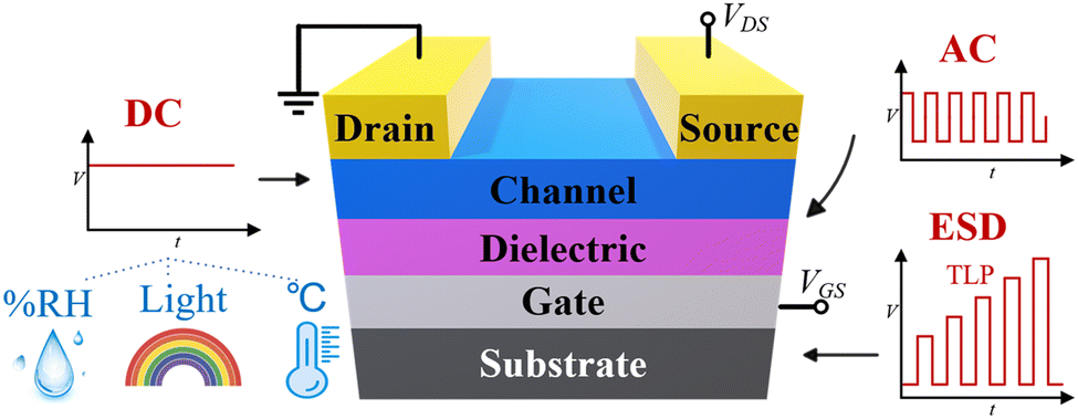 | ||
| Fig. 3 A schematic diagram of electrical performance and reliability testing of TFTs. | ||
As shown in Fig. 4, the electrical performance of TFTs is primarily evaluated based on 4 key parameters: subthreshold swing (SS), on/off current ratio (Ion/Ioff), threshold voltage (VTH), and μ. SS is a specific characteristic indicator reflecting the transition of TFTs from the off-state to the on-state, intuitively describing the steepness of the subthreshold region curve, and is defined as follows:
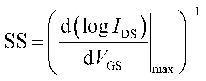 | (1) |
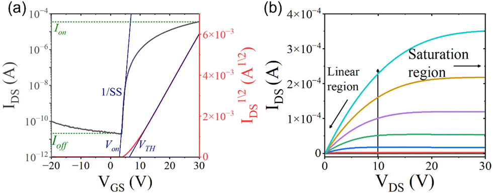 | ||
| Fig. 4 (a) Transfer curves and (b) output curves of a typical TFT. | ||
As shown in Fig. 4(a), its value is the reciprocal of the maximum slope of the subthreshold region. A steeper subthreshold region curve indicates a smaller SS value, suggesting a faster transition from the off-state to the on-state, resulting in faster response speed and lower power consumption.
I on/Ioff reflects the switching control capability of TFTs, defined as the ratio of the channel current in the on-state saturation (Ion) to the channel current in the off-state (Ioff). In flat panel display applications, TFTs often serve as pixel-switching devices. For practical applications, a lower off-state leakage current and a higher on-state leakage current are desirable, indicating that a higher Ion/Ioff is preferable.
V TH is one of the important indicators reflecting the electrical performance of TFTs, defined as VGS required to turn on TFTs. A lower VTH can effectively reduce the power consumption of TFTs.
μ is a crucial parameter characterizing the conductive properties of semiconductor materials, representing the average drift velocity of carriers (electrons or holes) under a unit electric field. Methods to extract μ of TFTs involve utilizing either the linear or saturation regions in the transfer curve. For lower VDS, the linear region is employed for extraction, while for higher VDS, the saturation region is utilized. The calculation formulae are given as follows:
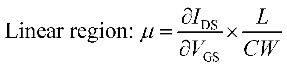 | (2) |
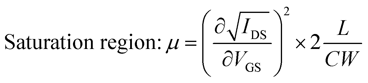 | (3) |
3.2. Reliability characterization of TFTs
As shown in Fig. 3, various working conditions are applied to evaluate the operational reliability of devices in specific environments. For achieving illumination-coupled bias stress stability, TFTs are simultaneously subjected to conditions of different intensities and wavelengths of light while applying bias stress to assess their reliability under combined electrical and optical stress. Temperature coupled bias stress stability refers to applying bias stress to TFTs at different ambient temperatures to measure their electrical stability. Ambient coupled bias stress stability involves monitoring the electrical stability of TFTs in environments with different gas compositions and ratios. AC stress stability can be used to evaluate the electrical reliability of TFTs by applying alternating stress, simulating their behaviour under near actual operating conditions.
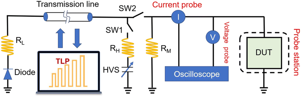 | ||
| Fig. 5 The setup diagram for ESD reliability characterization.100 | ||
In the reported ESD stress reliability tests of AOS TFTs, there are primarily three types of TFT connections, as illustrated in Fig. 6.100 In Fig. 6(a), the G and S electrodes are grounded, and the TLP pulse is applied to the D. This connection is the most commonly used for characterizing the ESD stress reliability of TFTs, allowing for an overall assessment of the TFTs’ ESD stress reliability and comparisons between the G insulator and the active layer. In Fig. 6(b), a varying DC bias is applied to the G, with the S grounded, and the TLP pulse applied to the D. This connection analyses the ESD stress reliability of TFTs by controlling the carrier density in the channel through the G voltage and manipulating the electric field between the G and D. In Fig. 6(c), the S and D electrodes are grounded, and the TLP pulse is applied to the G. This connection is used to analyze the impact of G dielectric degradation on the ESD stress reliability of TFTs.
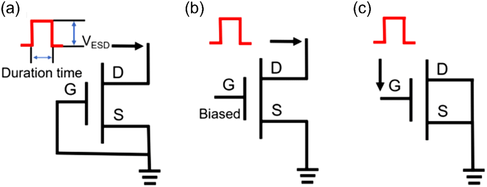 | ||
| Fig. 6 Connection modes in the TLP pulse test.100 | ||
4. Reliability research of AOS TFTs
4.1. Bias stress stability research of AOS TFTs
TFTs’ electrical bias stress stability is significantly influenced by the functional material characteristics24,104–109 and device structure.110,111 Therefore, researchers have focused on improving the electrical bias stress stability of AOS TFTs via active layer modification and device structure optimization.
Modifications to the active layer primarily aim to mitigate VO defects within the active layer or between the active layer and gate dielectric layer interface.112–114 In 2016, Heo et al. conducted a study on the effect of deep ultraviolet irradiation (DUV) annealing on the stability of a-IGZO TFTs as shown in Fig. 7.81 The study compared DUV annealing for 1 h, 2 h (1 h DUV, 2 h DUV), exposure to humid conditions after DUV annealing (DW), and DW samples following a second-time DUV treatment (DWD). For the DW TFTs, the H2O molecules infiltrate into the a-IGZO film, acting as donor ions, replacing the weakly bonded oxygen in the M–Ovac bonds and forming M–OH bonds within the a-IGZO film. M–OH bonds act as defects to capture free electrons, resulting in the poorest PBS stability of DW TFTs. However, for DWD TFTs, the OH bonds generated by additional H2O molecules at the VO sites are photoactivated, leading to an enhanced condensation reaction, subsequently forming stable metal–oxygen (M–O) bonds as shown in Fig. 7(b). This is manifested as ΔVTH values of 5.09 V (1 h DUV), 4.06 V (2 h DUV), 6.03 V (DW), and 2.44 V (DWD) for PBS (5 V, 10![[thin space (1/6-em)]](https://www.rsc.org/images/entities/char_2009.gif) 000 s) under atmospheric conditions as shown in Fig. 7(c). As shown in Fig. 8(a), in 2021, Kumar et al. attempted to optimize the electrical bias stress stability of TFTs by improving the film preparation process via synchronously performing H2 plasma treatment during a-IGZO deposition.112 Research indicates that compared to ΔVTH of untreated devices, ΔVTH of TFTs subjected to H2 plasma treatment under PBS (+2 V, 3000 s) and NBS (−2 V, 3000 s) is reduced by 51.56% and 63.04%, respectively (Fig. 9). According to PBS, the change in VTH is due to electron capture and migration to the ZrO2 layer at the a-IGZO/ZrO2 interface. Hydrogen, which acts as a shallow donor, can effectively passivate interface defects and enhance PBS stability. Under NBS, the decrease in device stability is believed to be due to H2O adsorption by the back channel of the a-IGZO TFT.115 When H2O captures holes from the valence band of the semiconductor, it forms positively charged H2O(s)+, which then attracts conduction electrons in the a-IGZO channel, resulting in a negative ΔVTH. After H2 plasma treatment, the Fermi level (Ef) is brought closer to the conduction band minimum (CBM). As shown in Fig. 8(b), this reduces the concentration of holes in the valence band of the active layer, effectively impeding the formation of H2O+, and thus reducing the negative ΔVTH.
000 s) under atmospheric conditions as shown in Fig. 7(c). As shown in Fig. 8(a), in 2021, Kumar et al. attempted to optimize the electrical bias stress stability of TFTs by improving the film preparation process via synchronously performing H2 plasma treatment during a-IGZO deposition.112 Research indicates that compared to ΔVTH of untreated devices, ΔVTH of TFTs subjected to H2 plasma treatment under PBS (+2 V, 3000 s) and NBS (−2 V, 3000 s) is reduced by 51.56% and 63.04%, respectively (Fig. 9). According to PBS, the change in VTH is due to electron capture and migration to the ZrO2 layer at the a-IGZO/ZrO2 interface. Hydrogen, which acts as a shallow donor, can effectively passivate interface defects and enhance PBS stability. Under NBS, the decrease in device stability is believed to be due to H2O adsorption by the back channel of the a-IGZO TFT.115 When H2O captures holes from the valence band of the semiconductor, it forms positively charged H2O(s)+, which then attracts conduction electrons in the a-IGZO channel, resulting in a negative ΔVTH. After H2 plasma treatment, the Fermi level (Ef) is brought closer to the conduction band minimum (CBM). As shown in Fig. 8(b), this reduces the concentration of holes in the valence band of the active layer, effectively impeding the formation of H2O+, and thus reducing the negative ΔVTH.
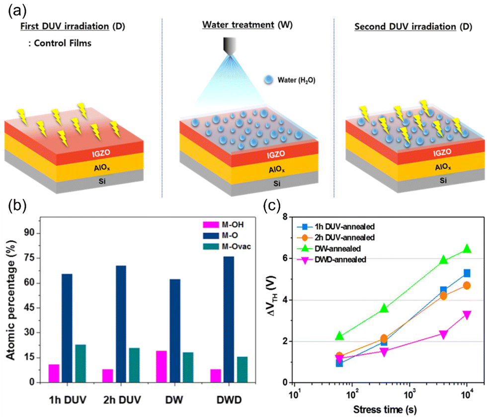 | ||
| Fig. 7 (a) Diagram of DUV and DWD treatment. (b) Summary of the relative metal–hydroxide (M–OH), metal oxide (M–O), and oxygen vacancy (M–Ovac) amounts under different annealing conditions. (c) Summary of the threshold voltage shifts of various processed a-IGZO TFTs. Reprinted with permission from J. S. Heo, J.-W. Jo, J. Kang, C.-Y. Jeong, H. Y. Jeong, S. K. Kim, K. Kim, H.-I. Kwon, J. Kim, Y.-H. Kim, M.-G. Kim and S. K. Park, ACS Appl. Mater. Interfaces, 2016, 8, 10403–10412.81 Copyright 2024 American Chemical Society. | ||
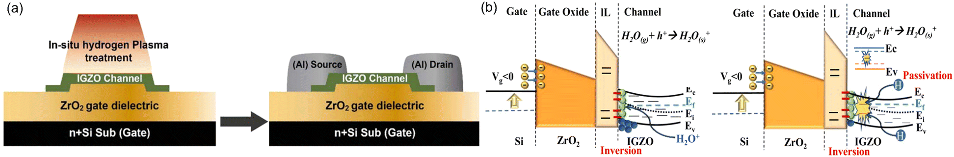 | ||
| Fig. 8 (a) A cross-sectional schematic of the staggered bottom gate a-IGZO TFTs. (b) Energy band diagrams of a-IGZO TFTs under NBS without and with in situ hydrogen plasma treatment. Reproduced with permission.112 Copyright 2024, J. H. Wu, Nanotechnology. | ||
 | ||
| Fig. 9 (a)–(d) Evolution of the transfer curves of a-IGZO TFTs under increasing PBS/NBS duration without and with in situ H2 plasma treatment. Reproduced with permission.112 Copyright 2024, J. H. Wu, Nanotechnology. | ||
When AOS TFTs are exposed to the air environment, H2O and O2 will penetrate from the back channel region of the AOS film, thereby affecting the electrical stability of TFTs.116 To mitigate this issue, researchers have employed structural optimization strategies, such as introducing a passivation layer between the active layer and the environment, which serves to reduce the impact of environmental factors on the active layer. This approach has been found to enhance the electrical bias stress stability of AOS TFTs.117,118
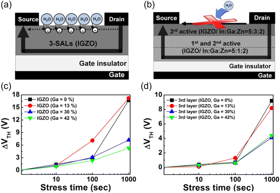
There is a strong bonding ability between Ga and O elements, which can suppress VO inside AOS films and improve electrical reliability. However, an excessive proportion of Ga elements can lead to the degradation of the device's electrical performance, resulting in a reduction in Ion and μ. As illustrated in Fig. 10(a) and (b), to enhance the environmental stability of AOS TFTs, in 2013, Kim et al. designed a self-passivated multi-stacked active layer (MSAL) a-IGZO thin film structure, utilizing a low Ga element ratio a-IGZO (In:Ga:Zn = 5:1:2) film as the channel transportation layer and employing a high Ga element ratio a-IGZO (In:Ga:Zn = 5:3:2) film as the barrier layer surrounding the back channel.119 As shown in Fig. 10(c) and (d), compared to conventional devices (single-layer a-IGZO thin film) (In:Ga:Zn = 5:1:2), the multilayer a-IGZO TFTs demonstrate high PBS (VGS = 20 V, VDS = 10 V, 1000 s) electrical reliability in ambient air, exhibiting a 40% reduction in the VTH shift.
 | ||
| Fig. 10 (a) and (b) Diagram of conventional a-IGZO and a-IGZO TFTs with MSAL. (c) and (d) ΔVTH of a-IGZO and a-IGZO TFTs with MSAL under 1000 s PBS stress. Reprinted with permission from D. J. Kim, Y. S. Rim and H. J. Kim, ACS Appl. Mater. Interfaces, 2013, 5, 4190–4194.119 Copyright 2024 American Chemical Society. | ||
In 2020, Corsino et al. employed ALD to create Al2O3 passivation layers for TFTs’ protection. They investigated the electrical bias stress stability of a-IGZO TFTs at various deposition temperatures.120 When the temperature is 200 °C, TFTs exhibit the best electrical stability with a VTH shift of only 0.3 V under PBS (20 V, 10000 s). Additionally, under NBS (−20 V, 10000 s), VTH of passivated TFTs approached 0 V. X-ray photoelectron spectroscopy (XPS) shows that when the passivation temperature is 200 °C, the peak area ratio of the M–O bond is the highest, and the peak area ratio of the M–VO bond is the lowest, indicating that the film has the lowest VO concentration. The peak area ratio of M–OH is also the lowest, indicating the lowest concentration of impurities such as hydroxyl and C, thus forming the densest Al2O3 with the least interface defects, which are beneficial for the electrical stability of TFTs.121
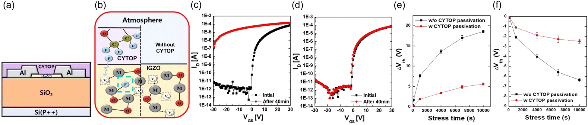
In 2020, Jung et al. proposed the use of functionalized CYTOP passivation layers to further enhance the environmental stability of a-IGZO TFTs as seen in Fig. 11(a). On the one hand, the surface of CYTOP films possesses strong hydrophobicity, which effectively resists the penetration of external H2O molecules.122
 | ||
| Fig. 11 (a) A schematic diagram of CYTOP passivated a-IGZO TFTs. (b) A diagram of F passivation. The transfer curves of TFTs sink in DI water without (c) and (d) with CYTOP passivation. ΔVTH according to the stress time under the PBS (e) and NBS (f), respectively. Reproduced with permission.122 Copyright 2024, J. Phys. D: Appl. Phys. | ||
As shown in Fig. 11(c) and (d), by comparing the electrical performance of TFTs soaked in water for 40 minutes, it is found that compared to untreated TFTs with severe degradation, CYTOP TFTs show almost no degradation. On the other hand, the F element in CYTOP diffuses into a-IGZO during the annealing process. Due to the similar ionic radii of F and O, the diffused F can easily replace VO in a-IGZO (Fig. 11(b)).122,123 Research shows that after F doping, the amount of VO in IGZO thin films decreases from 41.2% to 33.1%. Under the stress of PBS (VGS = 20 V, VDS = 10 V, 1000 s), the VTH shift is reduced by 40%. As depicted in Fig. 11(e) and (f), a-IGZO TFTs with CYTOP passivation layers exhibit better stability in both NBS and PBS. After 10000 s of PBS (20 V, 10000 s) and NBS (−20 V, 10000 s) tests under ambient conditions, the VTH shift of a-IGZO TFTs with CYTOP passivation is reduced by 54.37% and 62.70%, respectively.
In 2022, Lee et al. enhanced the electrical bias stress stability of TFTs by incorporating a homojunction (ITZO/ITZO) structure. As shown in Fig. 12 and 13, the homojunction consists of a UCL (oxygen-uncompensated channel layer) free of oxygen and a CCL (oxygen-compensated capping layer) containing oxygen. Additionally, a-ITZO TFTs with UCL alone are also fabricated for comparison.124 The presence of the oxygen-containing CCL effectively prevents the absorption of H2O and O2 by the UCL (Fig. 13). Compared to single-layer UCL TFTs, the bilayer UCL/CCL TFTs demonstrate superior stability under both PBS (30 V, 3600 s) and NBS (−30 V, 3600 s) conditions (Fig. 12(c)–(f)). In addition to modifying the active layer and optimizing the device structure, our group has recently achieved a significant improvement in the electrical bias stress stability of AOS TFTs through voltage modulation.125 By utilizing the interaction among ionized VO redistribution, the self-heating effect, and the hot carrier effect, a significant degradation reduction in AOS TFTs is achieved.
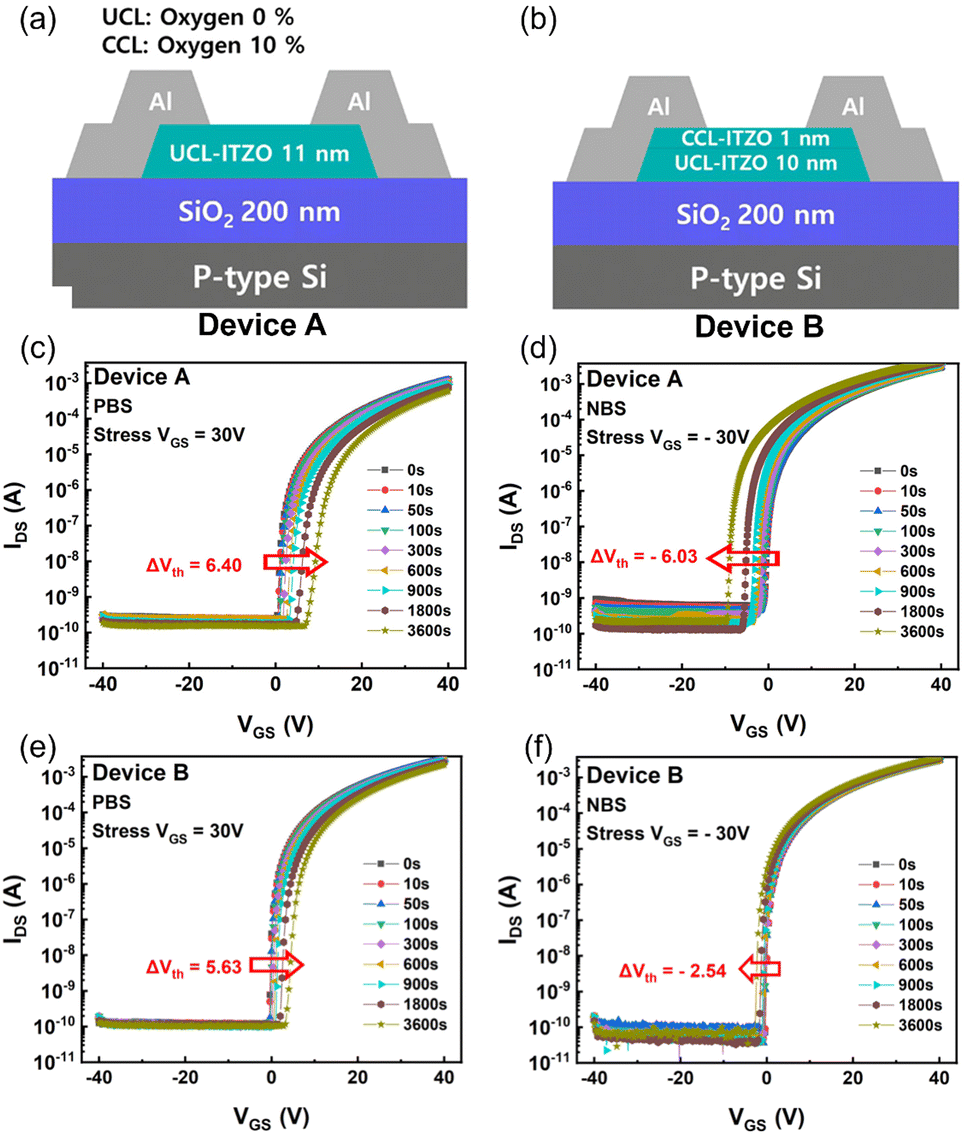 | ||
| Fig. 12 (a) ITZO TFTs with different channel structures: device A contains oxygen UCL, and device B contains a bilayer channel, which is an oxygen CCL and an oxygen UCL. Transfer of ITZO TFTs under PBS and NBS for 3600 s: (c) device A under PBS, (d) device A under NBS, (e) device B under PBS, and (f) device B under NBS. Reprinted with permission from J. Lee, J. Jin, S. Maeng, G. Choi, H. Kim and J. Kim, ACS Appl. Electron. Mater., 2022, 4, 1800–1806.124 Copyright 2024 American Chemical Society. | ||
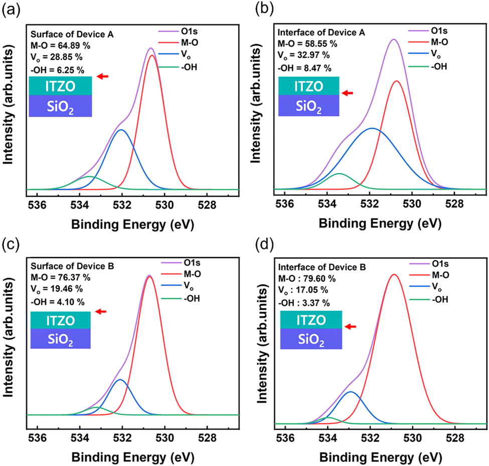 | ||
| Fig. 13 XPS O 1s spectral results of the (a) top surface of device A, (b) interface of device A, (c) top surface of device B, and (d) interface of device B. Reprinted with permission from J. Lee, J. Jin, S. Maeng, G. Choi, H. Kim and J. Kim, ACS Appl. Electron. Mater., 2022, 4, 1800–1806.124 Copyright 2024 American Chemical Society. | ||
In summary, the instability of PBS is mainly attributed to charge capture at the semiconductor/dielectric interface or within the dielectrics. For NBS, the ionization of VO is mainly caused by hole capture in the active layer and surface adsorption of H2O molecules. Material modification and embedding passivation layers are effective methods to improve the electrical reliability of AOS TFTs.
Fig. 14 reveals the mechanism of instability: under PBS/NBS, electron/hole trapping occurs at the G dielectric/active layer interface, leading to positive/negative ΔVTH. During NBIS, photo-generated carriers form electron–hole pairs, with positive charges migrating toward the G dielectric/active layer interface. Additionally, deep-level neutral VO defects are captured by holes and ionized, forming  or
or  , which are trapped at the interface, further exacerbating the negative ΔVTH due to hole de-trapping. In contrast, under PBIS, although holes are not trapped at the interface, illumination still leads to the formation of
  or
or  , resulting in a smaller negative ΔVTH, suppressing the positive shift caused by electron de-trapping.105,126–128 Furthermore, the degree of device degradation varies under different illumination conditions. At the same wavelength, high-intensity light further promotes the generation of electron–hole pairs, enhancing ΔVTH.10,105,128 When the light intensity remains constant, shorter wavelength light with higher energy causes a greater ΔVTH.127,129 To enhance the stability of TFTs under light stress, the main focus is on improving the anti-interference ability of the thin film itself or suppressing the entry of external light. This is achieved through process control to reduce VO defects and thereby enhance the film's inherent resistance to light,8,10,15,105,120,130–140 as well as by novel structural designs to mitigate external light interference.129,132,141–143
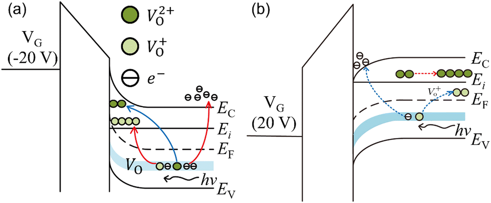 | ||
Fig. 14 Schematic energy-level diagrams of AOS TFTs under stresses of (a) NBIS and (b) PBIS, and the generation of  and and  . Reproduced with permission.126 Copyright 2024, Chinese Physics B. . Reproduced with permission.126 Copyright 2024, Chinese Physics B. | ||
In terms of process control, a common approach to improving stability is doping with elements that have strong binding energy with oxygen to suppress the formation of VO defects. These dopant elements include Hf,130 N,131,132,136,144 Sn,133 Mg,134 Pr,8 and graphene quantum dots (GQDs).127 In 2022, Lv et al. introduced N during the sputtering of a-IGZO and controlled the doping amount via the Ar:N2 ratio. As shown in Fig. 15(a)–(c), OI is usually attributed to O2− ions in the channel material (M–O bonds without oxygen deficiency), whereas OII to O2− is related to oxygen deficiency (VO) and OIII is related to adsorbed oxygen on the surface (e.g., H2O and O2). The introduction of N doping significantly suppresses the formation of VO defects. Fig. 15(d) and (e) demonstrate the impact of N doping on the device stability. With increasing N doping levels (Ar:N2 = 15:5), the VTH shift reduces, indicating better stability of TFTs.131 In addition to doping, high-quality thin-film deposition methods can also suppress the formation of VO defects and optimize device stability.15,135,136
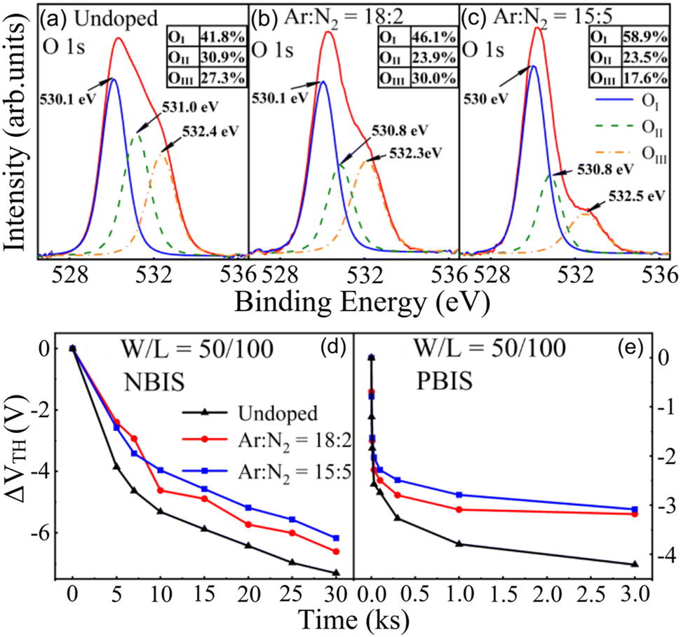 | ||
| Fig. 15 Measured and deconvoluted XPS spectra of O 1s for (a) undoped, (b) Ar/N2 = 18:2, and (c) Ar/N2 = 15:5. VTH degradation amount of TFTs with different N-doping conditions under (d) NBIS and (e) PBIS. Reproduced with permission.131 Copyright 2024, IEEE Transactions on Electron Devices. | ||
In 2019, Cho et al. compared sputtered and ALD-deposited a-IGZO films and found that due to the atomic-level control and gentler deposition process of ALD, it significantly reduces the formation of point defects such as VO and VM. In NBIS stability tests, ALD-prepared TFTs exhibit a 15.6% reduction in VO and a 60.3% decrease in ΔVTH compared to sputtered TFTs. In 2020, Liu et al. demonstrated that compared to sputtering, a-ITZO deposited by ultrasonic spray pyrolysis deposition exhibits a 6.9% reduction in VO defects. In NBIS stability tests, VTH shift is reduced by 38.9%, and in PBIS tests, VTH shift reduces by 9.6%.135 Furthermore, methods such as adjusting the oxide composition ratio in AOS films105 and optimizing the annealing temperature of AOS films145 and gate dielectric deposition temperature,134 as well as UV irradiation treatment137 can all regulate VO defects in AOS films and enhance the stability of TFTs under light.
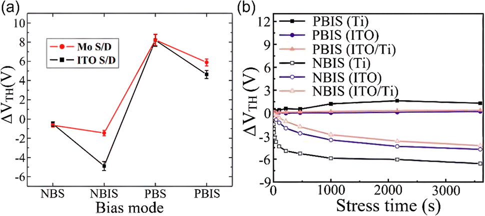
Another approach to enhance the stability of AOS TFTs under light is to use an optical shielding layer to reduce the influx of photons into the AOS film and suppress external light interference. In 2016, Park et al. compared the photostability of a-IGZO TFTs with ITO transparent electrodes and Mo opaque electrodes. The study finds that the two kinds of TFTs exhibit similar electrical properties. Fig. 16(a) demonstrates their reliability under electrical and optical stress, revealing comparable NBS and PBS stability. However, under illumination conditions, the photostability of the Mo opaque electrode device is significantly improved. Specifically, the negative VTH shift in NBIS decreased by 70.1% compared to the TFTs with ITO transparent electrodes, and the VTH shift in PBIS also reduced by 23.1%.141 In 2023, Li et al. inserted a 10 nm Ti layer between ITO and a-IGZO, also enhancing the photostability of TFTs. As shown in Fig. 16(b), the addition of the 10 nm Ti shielding layer reduces the VTH shift by 69.2% (PBIS) and 35.7% (NBIS) compared to TFTs with ITO electrodes.142
 | ||
| Fig. 16 (a) ΔVTH values of the IGZO TFTs using ITO and Mo electrodes under NBS, NBIS, PBS and PBIS conditions. (b) ΔVTH values of the IGZO TFTs using Ti, ITO and ITO/Ti electrodes under PBIS/NBIS conditions. Reproduced with permission.141,142 Copyright 2024, Journal of Electroceramics, ECS journal of solid state science and technology. | ||
Optimizing the preparation process of the active layer, such as annealing conditions,149 oxygen flow ratios,150 and doping,148 is beneficial for improving the quality of the film, thus optimizing the performance and reliability of TFTs.
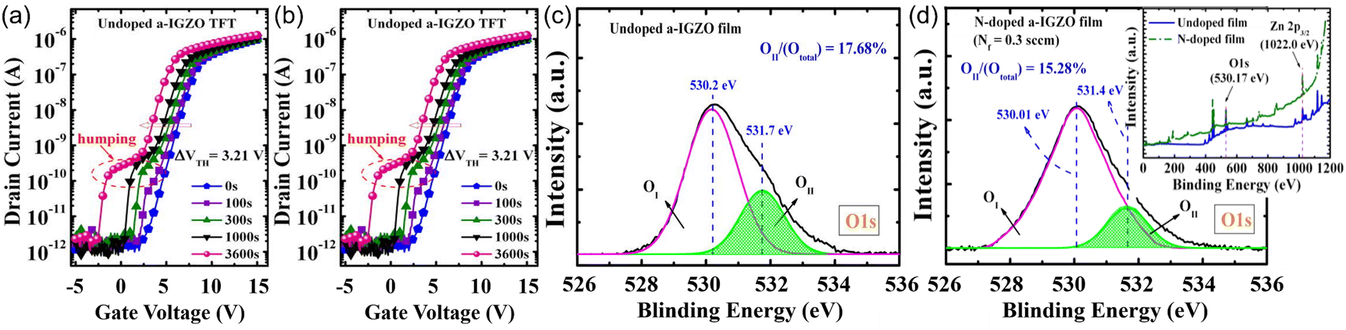
In 2013, Raja et al. studied the effect of N doping on the NBTS reliability of a-IGZO TFTs.148 Since the ionic radius of N is similar to that of O ions, N can be used as an alternative dopant for O, thus passivating trap states at the channel and the active layer/dielectric layer interface.155 At NBTS (60 °C, −20 V, 3600 s), a-IGZO:N TFTs showed no humping, and ΔVTH is 1.13 V compared to a-IGZO TFTs' ΔVTH of 3.21 V as shown in Fig. 17(a) and (b). By analyzing the XPS spectrum of the O 1s peak of a-IGZO and a-IGZO:N films, the peak intensity of a-IGZO:N thin films is higher, indicating that N is well bound to the a-IGZO matrix (the inset of Fig. 17(d)). Moreover, compared with the a-IGZO film, the OII peak intensity of the a-IGZO:N film is smaller, indicating that VO is suppressed, thereby improving the NBTS reliability of TFTs as shown in Fig. 17(c) and (d).
 | ||
| Fig. 17 NBTS stability of transfer curves of 20 V gate bias stressing at 333 K: (a) undoped and (b) N-doped a-IGZO devices. XPS spectra of the O 1s core level of (c) undoped a-IGZO film and (d) a-IGZO:N film. The inset depicts that the N sites are well incorporated in the a-IGZO matrix. Reproduced with permission.148 Copyright 2024, Applied Physics Letters. | ||
In 2016, Nakata et al. studied the impact of different oxygen flow ratios on the P/NBTS reliability of a-ITZO TFTs in the process of sputtering a-ITZO.150 At PBTS (70 °C, VGS = +10 V, 1000 s), with the increase of oxygen flow ratios, the electrical performance and the PBTS reliability of TFTs improve first and then decrease. A certain amount of oxygen can passivate the Vo within the a-ITZO conductive channel and at the active layer/dielectric layer interface. However, with further growth in the oxygen flow ratios, acceptor-like excess oxygen states (O0 or O−) will be formed inside the a-ITZO film. These acceptor-like states will trap electrons and form a more stable O2−, resulting in a positive ΔVTH. At NBTS (70 °C, −10 V, 1000 s), ΔVTH is not affected by the oxygen flow ratio, while H2O molecules in the air adsorbed by the channel can trap holes, making H+ dopants penetrate into the channel and act as a shallow donor-like, resulting in a negative VTH shift.56
In 2021, KW Park et al. used microwave annealing (MWA) and conventional thermal annealing (CTA) to prepare a-IGZO TFTs on a PI substrate and studied the electrical properties and P/NBTS reliability of TFTs.149 Compared with CTA, which needs to be carried out at a high temperature for a long time, MWA can transfer energy directly to the material's interior upon heat treatment using microwaves, so that there is no need for direct contact between the heating source and the heated material, and the active layer can be selectively and quickly heated, avoiding damage to the flexible substrate and the semiconductor layer. As shown in Fig. 18(a), at PBTS (25/55/85 °C, VGS = 2 V, 1000 s) and NBTS (25/55/85 °C, VGS = −2 V, 1000 s), MWA TFTs exhibit better reliability. The internal mechanism affecting device reliability is studied by extracting the characteristic charge trapping time (τ) from the time-dependence of ΔVTH under P/NBTS. As shown in Fig. 18(b), compared with CTA TFTs, the average effective energy barrier height for carrier transport (Eτ) of MWA TFTs is smaller, and the time required for carriers to be trapped inside the dielectric layer or the interface is longer. This indicates that MWA processing results in a more ordered a-IGZO crystal structure and fewer interface traps compared to CTA processing, thus improving the P/NBTS reliability of TFTs (Fig. 18(c)).156
 | ||
| Fig. 18 (a) Time dependence of the VTH shift under PBTS and NBTS tests at 25, 55, and 85 °C and (b) the ln(τ) as a function of reciprocal temperature (1/T) for CTA and MWA processed a-IGZO TFTs. (c) Subthreshold swing and interface trap density. Reproduced with permission.149 Copyright 2024, K.-W. Park. | ||
By optimizing the interface contact between the active layer and the dielectric layer, the temperature-coupled bias stress stability of TFTs can also be improved. In 2023, Choi et al. studied the influences of HfO2 as a dielectric layer for the PBTS reliability of a-IGZO TFTs,152 and prepared device A (HfO2, annealing under air at 400 °C), device B (HfO2, annealing under O2 at 400 °C) and device C (SiO2/HfO2, annealing under O2 at 400 °C) for comparison. Hydrogen-related defects can be easily introduced during HfO2 deposition using plasma-enhanced atomic layer deposition (PEALD), which may be present at the interstitial site (HO) and oxygen site (Hi+) of HfO2. At PBTS (80 °C, +6 V, 3600 s), the non-electroactive HO can be converted to Hi+ and diffused into the channel, thus increasing the role of a shallow donor-like, making the VTH of device A show an abnormal negative shift. While oxygen introduced in annealing eliminates hydrogen-related defects in HfO2, device B does not show an abnormal negative shift under PBTS. However, defects at the dielectric layer/active layer interface of device B trap electrons, resulting in a positive ΔVTH, so inserting a layer of a-SiO2 between a-IGZO and HfO2 (device C) effectively increases the conduction band offset energy and reduces interface trap density, and further improves the electrical reliability of TFTs.157
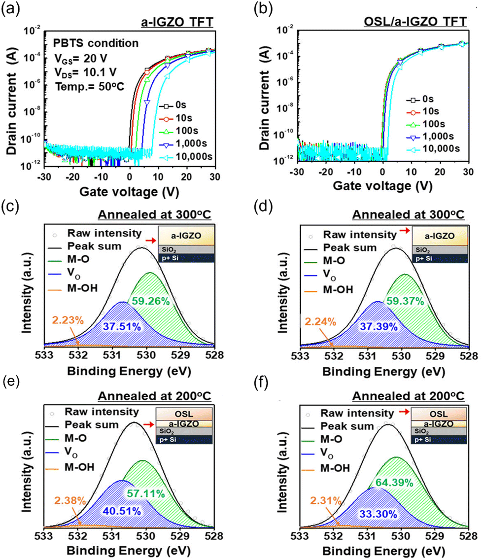
The introduction of the OSL can reduce the effect of thermal stress on the electrical instability of TFTs. In 2021, Kim et al. prepared dual-channel TFTs of a-IGZO and a-IGZO:Hf, in which a-IGZO:Hf was used as the OSL.154 At PBTS (50 °C, +20 V, 10000 s), OSL TFTs show better electrical reliability than non-OSL TFTs, ΔVTH reduces from 9.22 V to 2.21 V as shown in Fig. 19(a) and (b). Through XPS characterization, it is found that compared with non-OSL TFTs, there is more VO in the front channel of OSL TFTs, and the carrier concentration increases, thus improving the electrical performance of TFTs. Besides, the back channel has more M–O bonds and less VO, indicating that Hf adsorbs oxygen ions from a-IGZO,158 thereby inhibiting the adsorption of oxygen molecules in the atmosphere by the back channel and improving the stability of TFTs to PBTS as shown in Fig. 19(c)–(f).
 | ||
| Fig. 19 PBTS test results of the (a) a-IGZO TFT and (b) OSL/a-IGZO TFT. XPS results of the O 1s spectra of the (c) front channel and (d) back channel of the a-IGZO film annealed at 300 °C and of the (e) front channel and (f) back channel of the OSL/a-IGZO film annealed at 200 °C. Reprinted with permission from M. S. Kim, H. T. Kim, H. Yoo, D. H. Choi, J. W. Park, T. S. Kim, J. H. Lim and H. J. Kim, ACS Appl. Mater. Interfaces, 2021, 13, 31816–31824.154 Copyright 2024 American Chemical Society. | ||
In summary, the application of thermal stress on AOS TFTs will further aggravate ΔVTH caused by bias stress, and even show a unique humping phenomenon at high temperatures. Since the two kinds of stability are related to each other, the method of optimizing bias stress stability can also effectively reduce the temperature-coupled bias stress stability.
Under AC stress conditions, the main conditions for applying stress are VGS AC pulses159,160 and VDS AC pulses.160–163 For the degradation of AOS TFT caused by AC pulses, studies have proved that it is mainly affected by the dynamic hot carrier ejection (HCE).162–164 Taking the VGS AC pulse as an example, as shown in Fig. 20, before the falling edge of the pulse arrives, the carriers will be accumulated toward the interface between the active layer and the GI under positive Vg and captured by the trap at the interface (as shown in Fig. 20(b)). Subsequently, when the sufficiently steep falling edge of the pulse arrives, the positive Vg changes rapidly to negative, most of the carriers at the interface are discharged to the source/drain, the active layer is rapidly depleted and capacitively coupled a large Ex. The electrons, have been captured by the trap too late for discharging to the source/drain, are exposed to the large Ex and accelerated to become hot carriers (as shown in Fig. 20(c)). These high-energy hot carriers collide with the lattice, causing the nearby weak M–O bonds to break159 and generating defects. In addition, in TFTs, the emission of hot carriers will cause charges to overcome the interface barrier and inject into the dielectric layer, causing damage to the dielectric layer and forming trap charges.164 Both of these will raise the barrier between the S/D and the channel, thus positively shifting the transfer curve.
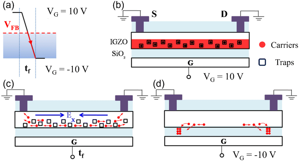 | ||
| Fig. 20 (a) The diagram of the applied AC bias voltage at the gate. (b) Carrier concentration at positive bias VFB before AC bias transition. (c) Most carriers deconcentrate during the transition time under flipping E-field. (d) Postponed carriers at the depletion region gain large energy, resulting in hot carrier ejection (HCE) causing damage in the nearby region. Reproduced with permission.164 Copyright 2024, Applied Physics Letters. | ||
To address the degradation of AOS TFTs caused by HCE phenomena due to AC bias stress, reducing the electric field in the depletion region and minimizing hot electron generation are feasible solutions. Early studies have indicated that using a passivation layer is a universal method to enhance the reliability of AOS TFTs under both static and dynamic bias stress.165 This paper focuses on elucidating the improvement of reliability under dynamic bias stress by regulating the properties of the AOS material itself. Strategies to enhance the reliability of AOS materials under AC bias stress include improving the quality of AOS thin films, increasing conductivity, adjusting the elemental ratio of AOS, and using overlapping AOS structures.
In 2023, Ho et al. compared the AC bias stress stability of a-IGZO and a-ITZO.161 After AC bias stress (f = 1 kHz, a duty ratio of 15%, and a transition time of 2 × 10⁻⁹ s, V0 = 0 V, VPP = 20 V), ΔVTH of a-IGZO (6:2:2), ITZO (1:1:2), ITZO (1:1:4), and ITZO (1:1:6) degrades by 69%, 28%, 17%, and 15% respectively. Compared with a-IGZO, due to the larger s-orbital radius of the Sn element in a-ITZO, the s-orbital has more overlapping areas, which is conducive to carrier transport on the ns orbit, making a-ITZO TFTs have higher field effect μ and current Ion/Ioff. Meanwhile, the Sn–O bond within the a-ITZO material exhibits a superior bonding strength of 528 kJ mol−1, surpassing the Ga–O bond in a-IGZO (354 kJ mol−1). This elevated bonding strength, to a certain degree, mitigates the likelihood of M–O bond fracture triggered by HCE under AC stress conditions, resulting in enhanced AC stress reliability of TFTs.
In 2024, Park et al. proposed to improve the AC stress reliability of AOS TFTs by stacking a layer of ZTO on the a-IGZO active layer.163 The key to this design strategy is to select suitable materials for energy band matching: the bottom layer uses narrow bandgap/high work function (Φ) materials, and the top layer uses large bandgap/small Φ materials, thereby forming an energy barrier through appropriate band bending between the two layers. The barrier can suppress the aggregation of charge carriers caused by AC stress and to some extent reduce the probability of generating HCE when AC stress flips. In addition, the study also found that a high proportion of Sn in ZTO films can enhance the stability of M–O bonds, further improving the AC stress reliability of TFTs.163,166
4.2. Electrostatic discharge reliability research of AOS TFTs
The phenomenon of ESD is ubiquitous in daily life and industrial production. When objects carrying two different types of charges approach each other, ESD occurs, generating high-voltage transient (ns-level) pulses. As a result, the insulating medium between the two objects may be electrically breached, forming a conductive pathway and neutralizing the charge transfer. Integrated circuits are susceptible to static electricity during processing, assembly, storage, and transportation. When ESD stress is applied to the circuit and devices, it can cause ESD damage and further lead to functional failure. ESD has become one of the most common threats to the reliability of electronic components. Therefore, it is imperative to implement ESD protection measures within the chip. Device-level ESD protection serves as the last line of defense, so enhancing the inherent ESD stress resistance of the device itself is crucial. Compared to DC/AC bias stress, ESD stress manifests as high-voltage instantaneous (ns-scale) pulses, which can cause irreparable damage to TFTs. This damage is characterized by an electrical breakdown or thermal burnout in the electrode, dielectric layer, and channel region, as illustrated in Fig. 21(a)–(e). During ESD breakdown in TFTs, significant fluctuations occur in the instantaneous current and voltage due to the breakdown event (Fig. 21(f)). Additionally, as the breakdown alters the conductivity, the I–V relationship captured under a subsequent DC bias application also undergoes corresponding changes (Fig. 21(g)).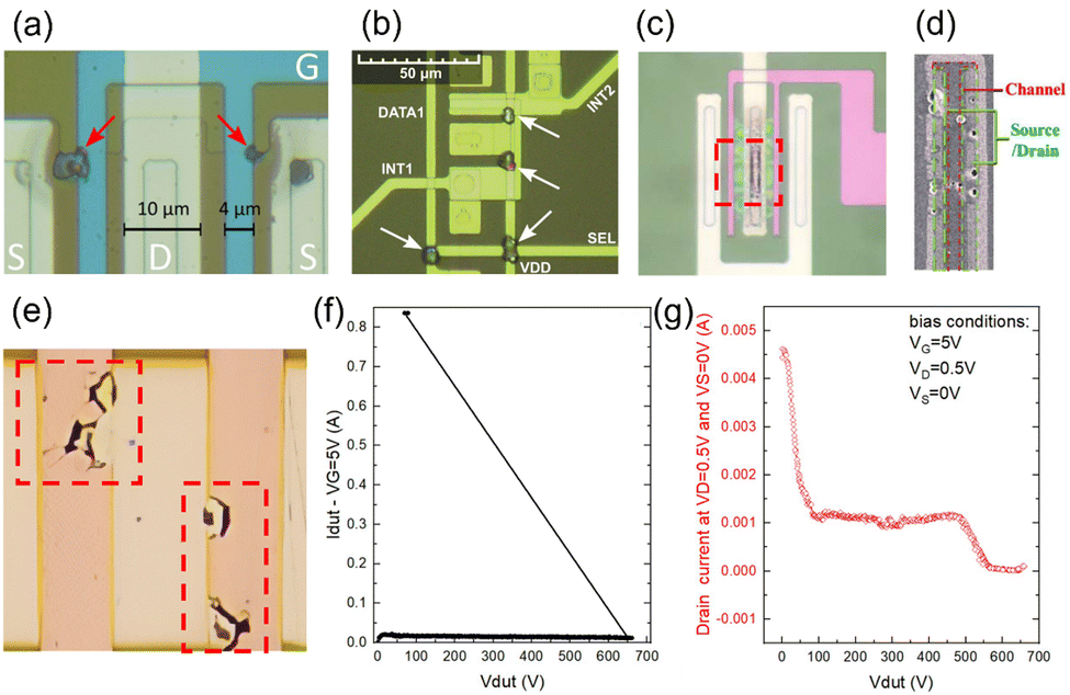 | ||
| Fig. 21 (a)–(e) Surface morphology of ESD stress-induced damage on TFTs. (f) ESD-induced fluctuations in transient voltage and current and (g) DC leakage current. Reproduced with permission.167–170 Copyright 2024, IEEE Journal of Display Technology, Microelectronics Reliability, M. Scholz, Microelectronics Reliability, respectively. | ||
Given that Si-based TFTs were the first to achieve industrialization, most of the reported research on ESD stress reliability of TFTs has focused primarily on p-Si and a-Si TFTs,171–176 with relatively fewer studies on AOS TFTs. Based on the currently available literature, AOS TFTs exhibit ESD characteristics that are similar to those of a-Si TFTs. In the ESD stress reliability testing of TFTs, the most common method involves applying a TLP pulse to the D electrode while grounding the S and G electrodes. This approach allows for the concurrent testing of the ESD robustness of both the active layer and the dielectric layer. Typically, in short-channel TFTs, large channel currents induced by ESD stress lead to overheating in the channel region, resulting in the generation and accumulation of a significant number of defect states, particularly near the D side. Ultimately, this can lead to the failure of TFTs. The destruction of the device manifests as burnout in the S-to-D path region.176 In long-channel TFTs, the increased channel resistance enhances the ESD robustness of the S-to-D path, leading to an enhancement in the ESD voltage required to cause device failure. Instead, the malfunction of TFTs is more commonly observed as a result of insulator breakdown between the D and G electrodes.177 Therefore, effective methods for improving the ESD robustness of AOS TFTs include reducing defects in the thin films along the breakdown path, optimizing film quality, and enhancing the thermal dissipation and anti-breakdown capabilities of TFTs. Readers interested in the ESD stress reliability of TFTs with various material types can refer to the comprehensive review by Yan et al.,100 and a detailed report on this topic will not be provided here.
4.3. Bending reliability research of AOS TFTs
In recent years, the flexible electronics industry has experienced rapid growth. The introduction of flexible electronics technology has broken through the limitations of traditional electronic devices, enabling them to better adapt to various complex environments and working conditions. This technology utilizes organic/inorganic materials to fabricate electronic devices on flexible/stretchable substrates, thus conferring greater flexibility and deformation capabilities to the devices. Such characteristics make flexible electronics promising for widespread application in areas such as wearable devices,178,179 medical equipment,180 and smart homes (IOTs).181,182 The advantages of AOS materials in flexible electronics are primarily reflected in their high μ, low-temperature preparation, excellent stability, and mechanical flexibility. These strengths position AOS as one of the key materials in the field of flexible electronics, driving continuous development and innovation in the technology.Based on the actual operating conditions of flexible TFTs in applications, bending stress tests can be categorized into static bending stress tests and dynamic bending stress tests. The primary factors influencing device degradation are the bending radius and the number of bending cycles. A smaller bending radius and a greater number of bending cycles result in more severe damage to the device. First, the bending process generates more defect states at the device interface and within the functional films, capturing carriers in the channel. Additionally, micro-cracks caused by device bending can lead to the infiltration of external H2O and O2, resulting in the degradation of the electrical performance and reliability of TFTs.183–185 In severe cases, this can even cause open circuits in the conductive channel and damage to the insulating layer, leading to the TFTs’ failure.
Research has found that there are significant differences in the bending stress resistance of various types of active layer thin film materials. As shown in Fig. 22, in 2019, Sheng et al. reported on the stability of IZO TFTs with In:Zn = 1:1 (11), a-IZTO TFTs with In:Zn:Sn = 1:1:1 (111) and In:Zn:Sn = 1:1:2 (112) under bias stress and bending stress.186 The study shows that the higher the proportion of the Sn element in the thin film, the better the stability of TFTs. As shown in Fig. 22(a), under PBTS stress (VGS = 20 V, T = 60 °C, tstress = 3600 s), the shift in VTH of a-IZO (11), a-IZTO (111), and a-IZTO (112) TFTs is 2.2 V, 1.8 V and 0.7 V, respectively. After 240000 dynamic bending stress, ΔVTH of a-IZTO (111) and a-IZTO (112) TFTs is about −1.7 V and −1.3 V. As shown in Fig. 22(b), in cyclic bending degradation, bending stress breaks the M–O bonds in AOS films, leading to a growth in the number of Vo+ related defect states within AOS,187–190 and the capture of electrons by defects leads to the degradation of VTH, μ, and SS of AOS TFTs. As the binding energy of Sn–O (528 kJ mol−1) is stronger than those of In–O (346 kJ mol−1) and Zn–O (250 kJ mol−1), compared to a-IZO, the increase in the Sn content in a-IZTO (111) and a-IZTO (112) facilitates the formation of more robust Sn–O bonds, better reducing the destruction of M–O bonds and the corresponding increase in defect states during bending. This is manifested in that the higher the proportion of Sn, the better the reliability under bending stress.
 | ||
| Fig. 22 (a) The transfer curve results of a-IZO (11), a-IZTO (111) and a-IZTO (112) TFTs under PBTS stress. (b) The ΔVTH, ΔSS and Δμ/μ% of a-IZTO (111) and a-IZTO (112) TFTs after 240000 bending cycles. Reprinted with permission from J. Sheng, T. Hong, D. Kang, Y. Yi, J. H. Lim and J.-S. Park, ACS Appl. Mater. Interfaces, 2019, 11, 12683–12692.186 Copyright 2024 American Chemical Society. | ||
Additionally, the introduction of a buffer layer to alleviate the destructive effects of bending stress on TFTs is an effective way to improve device reliability. As shown in Fig. 23, in 2020, Han et al. studied the bending stress reliability of a-IGZO TFTs with three types of buffer layers: a polyacrylic organic buffer layer (OB), an Al2O3 inorganic buffer layer (IB), and an Al2O3/PA/Al2O3 stacked buffer layer (HB).191 Among these, the OB TFTs failed quickly, while after 60000 bends (bending radius: 1.5 mm), ΔVTH of the IB and HB TFTs is −1.79 V and −0.44 V, Δμ is −0.98 cm2 V−1 s−1 and −0.31 cm2 V−1 s−1, and ΔSS is +0.02 V div−1 and +0.01 V div−1, respectively. Compared with IB TFTs, ΔVTH of HB TFTs is reduced by 75.42%, and the degradation of μ and SS is reduced by 68.37% and 50%, respectively, showing a better buffering effect against bending stress.
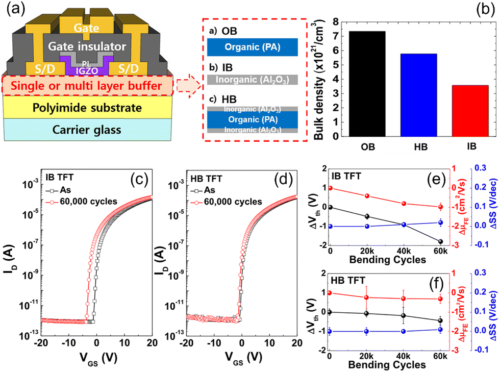 | ||
| Fig. 23 (a) Diagram of a-IGZO TFTs with buffer layers. The ΔVTH of transfer curves before and after 60000 bending cycles at a bending radius of 1.5 mm for (b) IB TFTs and (c) HB TFTs. Reprinted with permission from K.-L. Han, J.-H. Han, B.-S. Kim, H.-J. Jeong, J.-M. Choi, J.-E. Hwang, S. Oh and J.-S. Park, ACS Appl. Mater. Interfaces, 2020, 12, 3784–3791.191 Copyright 2024 American Chemical Society. | ||
4.4. Radiation reliability research of AOS TFTs
In some special application scenarios, such as space exploration, nuclear power plants, and medical radiologies, electronic devices will face severe ionizing radiation and be damaged. For semiconductor materials, high-energy photons present in X-rays or γ-rays produce photoelectrons, which further collide with adjacent atoms, with the final consequence of depositing the excess energy as electron–hole pairs and phonons, causing damage to the material structure. Taking Si-based TFTs as an example, they suffer from extreme degradation of electrical performance due to radiation exposure as s–p covalent semiconductors are sensitive to structural disorder caused by ionizing radiation. However, the conduction band of AOS originates from the overlap of s-orbitals and is relatively less insensitive to structural disturbances caused by ionizing radiation compared to those of other semiconductor materials, such as Si, organic, and two-dimensional materials. Therefore, the ionizing radiation reliability of AOS TFTs has gradually received attention in recent years.The early research on the ionizing radiation reliability of AOS TFTs mainly focused on binary materials, such as ZnO and IZO.192,193 Under γ-ray irradiation, TFTs exhibited good stability. In 2016, Cramer et al. compared the degradation behavior of IGZO TFTs and organic semiconductor TFTs under X-ray irradiation stress.194 They found that IGZO TFTs were able to maintain a near constant μ of 10 cm2 V−1 s−1 even after exposure to a total ionizing dose of 410 krad, while the transport performance of organic TFTs decreased by 55%. Unlike the charge transfer mechanism of AOS materials, organic semiconductors provide charge transfer pathways along the π-orbital system. This largely depends on the packing of organic molecules and their mutual orientation. The impact of X-ray radiation can cause irreversible damage to the material structure, leading to the degradation of TFT electrical performance. Although AOS TFTs have advantages in radiation reliability, there is still room for improvement. At present, the work on the ionizing radiation reliability of AOS TFTs mainly includes two categories: the material properties of AOS thin films themselves and the impact of introducing external passivation layers on radiation reliability. It is worth mentioning that the reliability of TFTs on ionizing radiation is influenced by various factors such as device structural parameters, material types, and radiation conditions, making it difficult to quantitatively compare the reliability between different articles.
As shown in Fig. 24, when ionizing radiation irradiates AOS films, under high-energy radiation irradiation, the oxygen–lattice bond in the channel material may be dissociated forming oxygen vacancies in the channel layer. Excessive oxygen vacancies make the channel material more sensitive to the working environment, and severe performance degradation may occur. Therefore, compared to a-IGZO materials, a-IWO and a-ITZO materials with higher oxygen bond dissociation energy exhibit better radiation resistance stability. However, excessive W or Sn can also suppress the number of oxygen vacancies, so it is necessary to optimize the proportion of different elements in the material to balance μ and reliability of the TFTs. The thickness of the AOS films is equally crucial for the radiation reliability of TFTs. In 2021, Shin et al. investigated the radiation reliability of a-IGTO TFTs with different thicknesses (12, 27, and 42 nm). Research has found that the thicker the thickness, the poorer the reliability of the device. As shown in Fig. 25, they think that due to the significantly higher energy of the incident proton particles compared to the displacement energy for the creation of Frenkel pairs in metal oxides, atoms ejected from their normal lattice positions can trigger multiple displacement chain reactions before leaving the film.195 When the thickness is large, each high-energy particle collides with atoms many times before leaving the film, resulting in more new high-energy atoms and vacancies. Therefore, even when the device is exposed to a proton beam with the same dose, there is a significant increase in the concentration of oxygen vacancies in the thicker channel IGTO TFTs. In 2023, Kang et al. investigated the radiation reliability of a-IZTO TFTs with different thicknesses (4, 5, and 6.2 nm) and found the same trend. They also found that the thickness of AOS thin films significantly affects the material's energy bandgap width and radiation absorption ability, which also has a significant impact on device reliability.
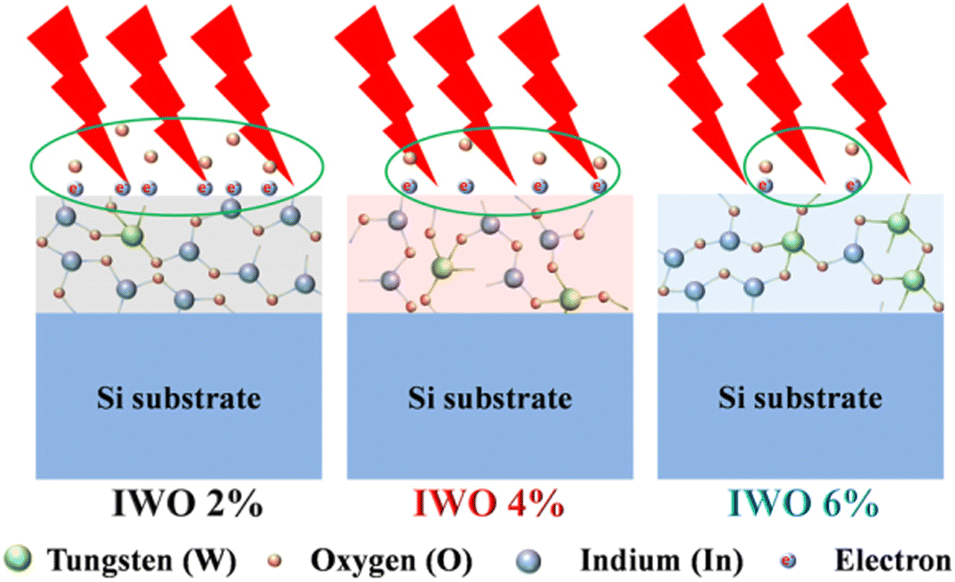 | ||
| Fig. 24 Schematic diagrams of the a-lWO channel material with varying WO contents after exposure to ionizing radiation, potentially illustrating the conceptual mechanism of radiation damage. Reproduced with permission.196 Copyright 2024, Applied Physics Letters. | ||
 | ||
| Fig. 25 Schematic diagram of the mechanism for a significant increase in the Ovac concentration in thicker IGTO thin films after proton irradiation based on the multiple displacement chain reaction model. Reproduced with permission.195 Copyright 2024, Surface and Interfaces. | ||
Introducing an external passivation layer such as Al2O3 has a significant effect on improving the electrical reliability of TFTs. With the increasing thickness of passivation layers, a greater number of displaced energetic atoms will be injected from Al2O3 into the AOS films, generating a higher concentration of oxygen vacancies and free electrons within the active layer, which reduces the radiation hardness of TFTs. Therefore, optimizing the thickness of the passivation layer to obtain oxide TFTs that exhibit excellent electrical stability and radiation robustness simultaneously is also important. Meanwhile, the process of optimization of the passivation layer also shows an effect on radiation reliability. Under the same thickness, using the sputtering method for preparing Al2O3 for the TFTs exhibits better radiation stability than the ALD method as the large amount of hydrogen in the Al2O3 layer grown by ALD will diffuse to the conductive channels and generate OH groups and free electrons, reducing the reliability of the device.
5. Conclusion and future prospects
In summary, the evolving landscape of active-matrix drive technologies necessitates significant advancements in the electrical performance and reliability of TFTs. While AOS TFTs have achieved commercial success in flat panel displays, enhancing clarity and refresh rates remains challenging. Therefore, the development of novel AOS materials that offer both high μ and stability is a crucial future research direction. Real-world operational environments introduce various complexities for TFTs. For instance, AOS TFTs are subjected to complex AC electrical stresses, and in the context of flexible electronics, they also endure diverse mechanical stresses due to bending. Consequently, a key trend in AOS TFT reliability research is to focus on the effects of complex electrical, mechanical, and combined stresses under actual operating conditions. Moreover, while academic research often relies on qualitative analysis, it is essential to establish quantitative correlations between device parameters and the reliability of AOS TFTs through comprehensive modelling. This quantitative understanding is vital for advancing the industrial application of AOS TFTs and bridging the gap between theoretical insights and practical implementation in next-generation display technologies.In addition to functioning as switches and current sources in displays, AOS TFTs have shown potential in various non-display applications such as sensors, memory, digital circuits, and neuromorphic computing. In these specific application scenarios, the external atmosphere and internal electrical stress types of AOS TFTs have unique characteristics. Research on repeatability, reliability, and stability is essential. However, research efforts in these areas are very limited and should therefore be an additional direction for reliability studies of AOS TFTs in preparation for non-display commercialization in the future.
Moreover, the integration of AOS TFTs with other devices has become a research hotspot. For example, TFT arrays are integrated with CMOS driver ICs and readout ICs (ROICs) through bonding processes to form functional modules. Additionally, the trend is towards more monolithic integration between TFTs and CMOS, either on or within the same substrate. To achieve compatibility of fabrication processes with other types of devices, the conditions for AOS TFT fabrication have become more stringent, and traditional optimization conditions based on independent devices will be limited, which poses a challenge to reliability optimization. This part of reliability work just begins.
Author contributions
Yuxuan Shen: conceptualization, investigation, and writing – original draft; Meng Zhang: investigation, validation, and writing – original draft; Siyuan He: investigation and writing – original draft; Le Bian: investigation and writing – original draft; Jiaxin Liu: investigation and writing – original draft; Zhengyu Chen: investigation; Shuangmei Xue: writing – review and editing; Ye Zhou: writing – review and editing; Yan Yan: conceptualisation, supervision, funding acquisition, project administration, investigation, visualisation, writing – original draft, and writing – review and editing.Data availability
No primary research results, software or code have been included and no new data were generated or analysed as part of this review.Conflicts of interest
The authors declare no competing financial interest.Acknowledgements
This work has been partially supported by the National Natural Science Foundation of China (grant no. 62374110), the Shenzhen Science and Technology Program (grant no. JCYJ20230808105806014), the State Key Laboratory of Radio Frequency Heterogeneous Integration (Independent Scientific Research Program no. 2024014) and the Shenzhen Municipal Research Program (grant no. SGDX20211123145404006).Notes and references
- C. Zhang, G. Liu, X. Geng, K. Wu and M. Debliquy, Sens. Actuators, A, 2020, 309, 112026 CrossRef CAS.
- S. Yu, J. Dong, H. Wang, S. Li, H. Zhu and T. Yang, J. Mater. Chem. A, 2022, 10, 25453–25462 RSC.
- S. Guo, L. Yang, X. Zhang, B. Dai, F. Geng, Z. Yang, P. Wang, G. Gao, L. Xu, J. Han, V. Ralchenko and J. Zhu, Ceram. Int., 2019, 45, 21590–21595 CrossRef CAS.
- P. P. Edwards, A. Porch, M. O. Jones, D. V. Morgan and R. M. Perks, Dalton Trans., 2004, 2995 RSC.
- H. Peelaers, E. Kioupakis and C. G. Van De Walle, Appl. Phys. Lett., 2019, 115, 082105 CrossRef.
- J. Shi, J. Zhang, L. Yang, M. Qu, D. Qi and K. H. L. Zhang, Adv. Mater., 2021, 33, 2006230 CrossRef CAS PubMed.
- K. Nomura, H. Ohta, A. Takagi, T. Kamiya, M. Hirano and H. Hosono, Nature, 2004, 432, 488–492 CrossRef CAS PubMed.
- H. Zhang, L. Liang, X. Wang, Z. Wu and H. Cao, IEEE Trans. Electron Devices, 2022, 69, 152–155 CAS.
- Z. Zheng, Y. Zeng, R. Yao, Z. Fang, H. Zhang, S. Hu, X. Li, H. Ning, J. Peng, W. Xie and X. Lu, J. Mater. Chem. C, 2017, 5, 7043–7050 RSC.
- B. Jing, C. Peng, M. Xu, H. Huang, X. Li and J. Zhang, IEEE Trans. Electron Devices, 2022, 69, 4283–4287 CAS.
- T. Shinozaki, K. Nomura, T. Katase, T. Kamiya, M. Hirano and H. Hosono, Thin Solid Films, 2010, 518, 2996–2999 CrossRef CAS.
- C. S. Yang, S. J. Huang, Y. C. Kao, G. H. Chen and W.-C. Chou, J. Cryst. Growth, 2015, 425, 258–261 CrossRef CAS.
- J.-Y. Lee, G. Tarsoly, S.-G. Choi, H.-G. Ryu and S.-J. Kim, Phys. Status Solidi A, 2021, 218, 2100205 CrossRef CAS.
- J. Sheng, J.-H. Han, W.-H. Choi, J. Park and J.-S. Park, ACS Appl. Mater. Interfaces, 2017, 9, 42928–42934 CrossRef CAS PubMed.
- M. H. Cho, H. Seol, A. Song, S. Choi, Y. Song, P. S. Yun, K.-B. Chung, J. U. Bae, K.-S. Park and J. K. Jeong, IEEE Trans. Electron Devices, 2019, 66, 1783–1788 CAS.
- M. H. Cho, C. H. Choi, H. J. Seul, H. C. Cho and J. K. Jeong, ACS Appl. Mater. Interfaces, 2021, 13, 16628–16640 CrossRef CAS PubMed.
- J. B. Ko and S.-H. K. Park, Mater. Lett., 2024, 363, 136297 CrossRef CAS.
- W. Zhang and X. Wen, in Semiconducting Metal Oxide Thin-Film Transistors, ed. Y. Zhou, IOP Publishing, 2020, pp. 12 Search PubMed.
- T.-H. Shih, H.-C. Ting, C.-L. Chen, L. Tsai, C.-Y. Chen, L.-F. Lin, H.-S. Lin, L.-H. Chang and Y.-H. Lin, 2014 21st International Workshop on Active-Matrix Flatpanel Displays and Devices (AM-FPD), IEEE, Kyoto, Japan, 2014, pp.17–20 Search PubMed.
- Q. Zhang, F. K. Shan, G. X. Liu, A. Liu, W. J. Lee and B. C. Shin, J. Korean Phys. Soc., 2014, 64, 1514–1518 CrossRef CAS.
- P. F. Carcia, R. S. McLean, M. H. Reilly and G. Nunes, Appl. Phys. Lett., 2003, 82, 1117–1119 CrossRef CAS.
- Y.-S. Park, H.-K. Park, J.-A. Jeong, H.-K. Kim, K.-H. Choi, S.-I. Na and D.-Y. Kim, J. Electrochem. Soc., 2009, 156, H588 CrossRef CAS.
- N. R. Armstrong, P. A. Veneman, E. Ratcliff, D. Placencia and M. Brumbach, Acc. Chem. Res., 2009, 42, 1748–1757 CrossRef CAS PubMed.
- Y. Zhang, H. Zhang, J. Yang, X. Ding and J. Zhang, IEEE Trans. Electron Devices, 2019, 66, 5170–5176 CAS.
- W.-K. Lin, K.-C. Liu, S.-T. Chang and C.-S. Li, Thin Solid Films, 2012, 520, 3079–3083 CrossRef CAS.
- H. He, H. Huang, C. Peng, G. Liu, J. Liu, S. Duan, B. Zou and D. Wan, J. Mater. Chem. C, 2024, 12, 607–613 RSC.
- Y. J. Tak, S. J. Kim, S. Kwon, H. J. Kim, K.-B. Chung and H. J. Kim, J. Mater. Chem. C, 2018, 6, 249–256 RSC.
- J. Kim, N. Miyokawa, K. Ide, Y. Toda, H. Hiramatsu, H. Hosono and T. Kamiya, AIP Adv., 2016, 6, 015106 CrossRef.
- X. Liu, W. Kuang, H. Ni, Z. Tao, J. Chang, Q. Liu, J. Ge, C. Li and Q. Dai, Small, 2018, 14, 1800265 CrossRef PubMed.
- J. Ma, S. Jia, X. Qu, H. Tang, B. Xu, Z. Wu, P. Liu, K. Wang, X. Yang, W. Xu and X. W. Sun, J. Soc. Inf. Disp., 2022, 30, 585–592 CrossRef CAS.
- N. Mastour, K. Ramachandran, S. Ridene, K. Daoudi and M. Gaidi, Eur. Phys. J. Plus, 2022, 137, 1137 CrossRef CAS.
- Z. Xia, in Semiconducting Metal Oxide Thin-Film Transistors, ed. Y. Zhou, IOP Publishing, 2020, p. 7 Search PubMed.
- J. Yeon Kwon and J. Kyeong Jeong, Semicond. Sci. Technol., 2015, 30, 024002 CrossRef.
- K. Jenifer, S. Arulkumar, S. Parthiban and J. Y. Kwon, J. Electron. Mater., 2020, 49, 7098–7111 CrossRef.
- G. W. Shim, W. Hong, J. Cha, J. H. Park, K. J. Lee and S. Choi, Adv. Mater., 2020, 32, 1907166 CrossRef CAS PubMed.
- K. Myny, Nat. Electron., 2018, 1, 30–39 CrossRef CAS.
- N. Tiwari, A. Nirmal, M. R. Kulkarni, R. A. John and N. Mathews, Inorg. Chem. Front., 2020, 7, 1822–1844 RSC.
- S. Kim and H. Yoo, Micromachines, 2022, 13, 2258 CrossRef PubMed.
- M. Zhang, W. Zhou, R. Chen, M. Wong and H.-S. Kwok, IEEE Electron Device Lett., 2017, 38, 52–55 CAS.
- M. Zhang, Y. Yan, G. Li, S. Deng, W. Zhou, R. Chen, M. Wong and H.-S. Kwok, IEEE Electron Device Lett., 2018, 39, 1684–1687 CAS.
- C. H. Champness and C. H. Chan, Sol. Energy Mater. Sol. Cells, 1995, 37, 75–92 CrossRef CAS.
- Z. Zhao, D. L. Morel and C. S. Ferekides, Thin Solid Films, 2002, 413, 203–211 CrossRef CAS.
- P. Ghosh, Sol. Energy Mater. Sol. Cells, 2004, 81, 279–289 CrossRef CAS.
- J. Godt, F. Scheidig, C. Grosse-Siestrup, V. Esche, P. Brandenburg, A. Reich and D. A. Groneberg, J. Occup. Med. Toxicol., 2006, 1, 22 CrossRef PubMed.
- D. Zhang, C. Li, S. Han, X. Liu, T. Tang, W. Jin and C. Zhou, Appl. Phys. Lett., 2003, 82, 112–114 CrossRef CAS.
- R. L. Hoffman, J. Appl. Phys., 2004, 95, 5813–5819 CrossRef CAS.
- R. E. Presley, C. L. Munsee, C.-H. Park, D. Hong, J. F. Wager and D. A. Keszler, J. Phys. D: Appl. Phys., 2004, 37, 2810–2813 CrossRef CAS.
- G. F. Boesen and J. E. Jacobs, Proc. IEEE, 1968, 56, 2094–2095 Search PubMed.
- R. L. Hoffman, B. J. Norris and J. F. Wager, Appl. Phys. Lett., 2003, 82, 733–735 CrossRef CAS.
- S. Parthiban and J.-Y. Kwon, J. Mater. Res., 2014, 29, 1585–1596 CrossRef CAS.
- T. Kamiya and H. Hosono, NPG Asia Mater., 2010, 2, 15–22 CrossRef.
- J. K. Jeong, J. Mater. Res., 2013, 28, 2071–2084 CrossRef CAS.
- M. P. Taylor, D. W. Readey, M. F. A. M. Van Hest, C. W. Teplin, J. L. Alleman, M. S. Dabney, L. M. Gedvilas, B. M. Keyes, B. To, J. D. Perkins and D. S. Ginley, Adv. Funct. Mater., 2008, 18, 3169–3178 CrossRef CAS.
- Y. Zhu, Y. He, S. Jiang, L. Zhu, C. Chen and Q. Wan, J. Semicond., 2021, 42, 031101 CrossRef CAS.
- H. Hosono, J. Non-Cryst. Solids, 2006, 352, 851–858 CrossRef CAS.
- T. Kamiya, K. Nomura and H. Hosono, J. Display Technol., 2009, 5, 273–288 CAS.
- C.-J. Kim, S. Kim, J.-H. Lee, J.-S. Park, S. Kim, J. Park, E. Lee, J. Lee, Y. Park, J. H. Kim, S. T. Shin and U.-I. Chung, Appl. Phys. Lett., 2009, 95, 252103 CrossRef.
- K. Nomura, H. Ohta, K. Ueda, T. Kamiya, M. Hirano and H. Hosono, Science, 2003, 300, 1269–1272 CrossRef CAS PubMed.
- E. Fukumoto, T. Arai, N. Morosawa, K. Tokunaga, Y. Terai, T. Fujimori and T. Sasaoka, J. Soc. Inf. Disp., 2011, 19, 867–872 CrossRef CAS.
- J. H. Song, K. S. Kim, Y. G. Mo, R. Choi and J. K. Jeong, IEEE Electron Device Lett., 2014, 35, 853–855 CAS.
- F. Chen, M. Zhang, Y. Wan, X. Xu, M. Wong and H.-S. Kwok, J. Semicond., 2023, 44, 091602 CrossRef.
- H. Li, M. Qu and Q. Zhang, IEEE Electron Device Lett., 2013, 34, 1268–1270 CAS.
- T. Kizu, N. Mitoma, M. Miyanaga, H. Awata, T. Nabatame and K. Tsukagoshi, J. Appl. Phys., 2015, 118, 125702 CrossRef.
- D.-B. Ruan, P.-T. Liu, K.-J. Gan, Y.-C. Chiu, M.-C. Yu, T.-C. Chien, Y.-H. Chen, P.-Y. Kuo and S. M. Sze, Thin Solid Films, 2018, 666, 94–99 CrossRef CAS.
- J.-M. Lee, I.-T. Cho, J.-H. Lee and H.-I. Kwon, Appl. Phys. Lett., 2008, 93, 093504 CrossRef.
- W. Xu, M. Xu, J. Jiang, S. Xu and X. Feng, IEEE Trans. Electron Devices, 2019, 66, 2219–2223 CAS.
- S.-H. Choi, IEEE Electron Device Lett., 2021, 42, 168–171 CAS.
- J. Kim, J. Park, G. Yoon, A. Khushabu, J.-S. Kim, S. Pae, E.-C. Cho and J. Yi, Mater. Sci. Semicond. Process., 2020, 120, 105264 CrossRef CAS.
- Y. Yu, N. Lv, D. Zhang, Y. Wei and M. Wang, IEEE Electron Device Lett., 2021, 42, 1480–1483 CAS.
- S. Samanta, U. Chand, S. Xu, K. Han, Y. Wu, C. Wang, A. Kumar, H. Velluri, Y. Li, X. Fong, A. V.-Y. Thean and X. Gong, IEEE Electron Device Lett., 2020, 41, 856–859 CAS.
- M. Ryu, K. Park, J. Seon and S. Y. Lee, J. Soc. Inf. Disp., 2010, 18, 734–744 CrossRef CAS.
- K.-S. Kim, Y.-H. Hwang, I. Hwang and W.-J. Cho, J. Korean Phys. Soc., 2014, 65, 399–403 CrossRef CAS.
- W. Lee, W. Park, S. Park, S. Sung, Y. Noh and M. Yoon, Adv. Mater., 2015, 27, 5043–5048 CrossRef CAS PubMed.
- S. Sanctis, N. Koslowski, R. Hoffmann, C. Guhl, E. Erdem, S. Weber and J. J. Schneider, ACS Appl. Mater. Interfaces, 2017, 9, 21328–21337 CrossRef CAS PubMed.
- W. Xu, L. Hu, C. Zhao, L. Zhang, D. Zhu, P. Cao, W. Liu, S. Han, X. Liu, F. Jia, Y. Zeng and Y. Lu, Appl. Surf. Sci., 2018, 455, 554–560 CrossRef CAS.
- S. Sanctis, R. C. Hoffmann, M. Bruns and J. J. Schneider, Adv. Mater. Interfaces, 2018, 5, 1800324 CrossRef.
- S. Sanctis, R. C. Hoffmann, N. Koslowski, S. Foro, M. Bruns and J. J. Schneider, Chem. – Asian J., 2018, 13, 3912–3919 CrossRef CAS PubMed.
- N. Koslowski, S. Sanctis, R. C. Hoffmann, M. Bruns and J. J. Schneider, J. Mater. Chem. C, 2019, 7, 1048–1056 RSC.
- S.-B. Ji, N. Seong, J. Park, H. Im, Y.-S. Kim and Y. Hong, ACS Appl. Electron. Mater., 2023, 5, 1035–1040 CrossRef CAS.
- W. Kim, W. Lee, T. Kwak, S. Baek, S. Lee and S. Park, Adv. Mater. Interfaces, 2022, 9, 2200032 CrossRef CAS.
- J. S. Heo, J.-W. Jo, J. Kang, C.-Y. Jeong, H. Y. Jeong, S. K. Kim, K. Kim, H.-I. Kwon, J. Kim, Y.-H. Kim, M.-G. Kim and S. K. Park, ACS Appl. Mater. Interfaces, 2016, 8, 10403–10412 CrossRef CAS PubMed.
- E. Carlos, R. Branquinho, A. Kiazadeh, J. Martins, P. Barquinha, R. Martins and E. Fortunato, ACS Appl. Mater. Interfaces, 2017, 9, 40428–40437 CrossRef CAS PubMed.
- C.-J. Moon and H.-S. Kim, ACS Appl. Mater. Interfaces, 2019, 11, 13380–13388 CrossRef CAS PubMed.
- W. Lee, S. Choi, J. Kim, S. K. Park and Y. Kim, Adv. Electron. Mater., 2019, 5, 1900073 CrossRef.
- T.-T. Yang, D.-H. Kuo and K.-P. Tang, J. Non-Cryst. Solids, 2021, 553, 120503 CrossRef CAS.
- J. Sheng, J.-H. Lee, W.-H. Choi, T. Hong, M. Kim and J.-S. Park, J. Vac. Sci. Technol., A, 2018, 36, 060801 CrossRef.
- Y.-M. Kim, H.-B. Kang, G.-H. Kim, C.-S. Hwang and S.-M. Yoon, IEEE Electron Device Lett., 2017, 38, 1387–1389 CAS.
- S. Sanctis, J. Krausmann, C. Guhl and J. J. Schneider, J. Mater. Chem. C, 2018, 6, 464–472 RSC.
- M. I. Büschges, R. C. Hoffmann, A. Regoutz, C. Schlueter and J. J. Schneider, Chem. – Eur. J., 2021, 27, 9791–9800 CrossRef PubMed.
- M. I. Büschges, V. Trouillet and J. J. Schneider, J. Mater. Chem. C, 2022, 10, 5447–5457 RSC.
- S.-H. Moon, S.-H. Bae, Y. H. Kwon, N.-J. Seong, J.-H. Yang, Y.-H. Kim, K.-J. Choi, C.-S. Hwang and S.-M. Yoon, ACS Appl. Electron. Mater., 2021, 3, 4849–4858 CrossRef CAS.
- T. Hong, Y. Kim, S. Choi, J. H. Lim and J. Park, Adv. Electron. Mater., 2023, 9, 2201208 CrossRef CAS.
- Z. Chen, J. Yang, X. Ding, X. Li and J. Zhang, IEEE Trans. Electron Devices, 2024, 71, 1963–1968 CAS.
- D.-G. Kim, H. Choi, Y.-S. Kim, D.-H. Lee, H.-J. Oh, J. H. Lee, J. Kim, S. Lee, B. Kuh, T. Kim, H. Y. Kim and J.-S. Park, ACS Appl. Mater. Interfaces, 2023, 15, 31652–31663 CrossRef CAS PubMed.
- B. Lu, F. Zhuge, Y. Zhao, Y.-J. Zeng, L. Zhang, J. Huang, Z. Ye and J. Lu, Curr. Opin. Solid State Mater. Sci., 2023, 27, 101092 CrossRef CAS.
- J. Y. Choi and S. Y. Lee, J. Korean Phys. Soc., 2017, 71, 516–527 CrossRef CAS.
- S. Y. Lee, Trans. Electr. Electron. Mater., 2020, 21, 235–248 CrossRef.
- H. J. Kim, K. Park and H. J. Kim, J. Soc. Inf. Disp., 2020, 28, 591–622 CrossRef CAS.
- Y. Wang and Y. Wang, IEEE Trans. Electron Devices, 2020, 67, 3775–3780 Search PubMed.
- Y. Yan, W. Lan, Y. Chen, D. Yang, Y. Zhou, Z. Zhu and J. J. Liou, Adv. Electron. Mater., 2022, 8, 2100886 CrossRef CAS.
- F. John, IEEE Trans. Device Mater. Relib., 2010, 10, 460–475 Search PubMed.
- C.-L. Chen, W.-F. Chen, L. Zhou, W.-J. Wu, M. Xu, L. Wang and J.-B. Peng, AIP Adv., 2016, 6, 035025 CrossRef.
- A. Suresh and J. F. Muth, Appl. Phys. Lett., 2008, 92, 033502 CrossRef.
- D. Geun Lee, H. Chul Yoo, E.-K. Hong, W.-J. Cho and J. Tae Park, 1 Dept. of Electronics Eng., Incheon National Univ., Incheon, 406-772, Korea, and 2 Dept. of Electronic Materials Eng., Kwangwoon Univ., Seoul, 139-701, Korea, AIMS Mater. Sci., 2020, 7, 596–607 Search PubMed.
- J.-H. Kim, E.-K. Park, M. S. Kim, H. J. Cho, D.-H. Lee, J.-H. Kim, Y. Khang, K. Park and Y.-S. Kim, Thin Solid Films, 2018, 645, 154–159 CrossRef CAS.
- N. N. Mude, R. N. Bukke, J. K. Saha, C. Avis and J. Jang, Adv. Electron. Mater., 2019, 5, 1900768 CrossRef CAS.
- M. Zhang, Z. Jiang, S. Deng, Z. Chen, X. Ma, C.-H. Tien, L.-C. Chen, M. Wong and H.-S. Kwok, IEEE Electron Device Lett., 2023, 44, 1124–1127 CAS.
- Z. Jiang, M. Zhang, S. Deng, Y. Yang, M. Wong and H.-S. Kwok, IEEE Electron Device Lett., 2022, 43, 886–889 CAS.
- Z. Jiang, M. Zhang, S. Deng, M. Wong and H.-S. Kwok, IEEE Trans. Electron Devices, 2023, 70, 6381–6386 CAS.
- J. C. Park and H.-N. Lee, IEEE Electron Device Lett., 2012, 33, 818–820 CAS.
- D. Ho, H. Jeong, S. Choi and C. Kim, J. Mater. Chem. C, 2020, 8, 14983–14995 RSC.
- O. K. Prasad, S. K. Mohanty, C. H. Wu, T. Y. Yu and K. M. Chang, Nanotechnology, 2021, 32, 395203 CrossRef CAS PubMed.
- H. Xiong, L. Fang, F. Wu, D. Liu, Z. Yuan, G. Liu, S. Zhang, H. Zhang, W. Li, P. Yu and C. Tong, Symp. Dig. Tech. Papers, 2023, 54, 90–93 CrossRef.
- J. Su, R. Li, Y. Ma, S. Dai, Y. Wang, H. Yang and X. Zhang, J. Alloys Compd., 2019, 801, 33–39 CrossRef CAS.
- S. Choi, J.-Y. Kim, H. Kang, D. Ko, J. Rhee, S.-J. Choi, D. M. Kim and D. H. Kim, Materials, 2019, 12, 3149 CrossRef CAS PubMed.
- S.-Y. Sung, J. H. Choi, U. B. Han, K. C. Lee, J.-H. Lee, J.-J. Kim, W. Lim, S. J. Pearton, D. P. Norton and Y.-W. Heo, Appl. Phys. Lett., 2010, 96, 102107 CrossRef.
- Y. Shi, Y.-S. Shiah, K. Sim, M. Sasase, J. Kim and H. Hosono, Appl. Phys. Lett., 2022, 121, 212101 CrossRef CAS.
- W. Zhong, R. Yao, Y. Liu, L. Lan and R. Chen, IEEE Trans. Electron Devices, 2020, 67, 3157–3162 CAS.
- D. J. Kim, Y. S. Rim and H. J. Kim, ACS Appl. Mater. Interfaces, 2013, 5, 4190–4194 CrossRef CAS PubMed.
- D. C. Corsino, J. P. S. Bermundo, M. N. Fujii, K. Takahashi, Y. Ishikawa and Y. Uraoka, J. Phys. D: Appl. Phys., 2020, 53, 165103 CrossRef CAS.
- J. S. Park, T. S. Kim, K. S. Son, K.-H. Lee, W.-J. Maeng, H.-S. Kim, E. S. Kim, K.-B. Park, J.-B. Seon, W. Choi, M. K. Ryu and S. Y. Lee, Appl. Phys. Lett., 2010, 96, 262109 CrossRef.
- K.-M. Jung, J. Oh, H. E. Kim, A. Schuck, K. Kim, K. Park, J.-H. Jeon, S.-Y. Lee and Y.-S. Kim, J. Phys. D: Appl. Phys., 2020, 53, 355107 CrossRef CAS.
- J.-S. Seo, J.-H. Jeon, Y. H. Hwang, H. Park, M. Ryu, S.-H. K. Park and B.-S. Bae, Sci. Rep., 2013, 3, 2085 CrossRef PubMed.
- J. Lee, J. Jin, S. Maeng, G. Choi, H. Kim and J. Kim, ACS Appl. Electron. Mater., 2022, 4, 1800–1806 CrossRef CAS.
- G. Zhu, M. Zhang, Z. Jiang, J. Huang, Y. Huang, S. Deng, L. Lu, M. Wong and H.-S. Kwok, IEEE Trans. Electron Devices, 2023, 70, 4198–4205 CAS.
- J. Guo, D. Zhang, M. Wang and H. Wang, Chin. Phys. B, 2021, 30, 118102 CrossRef CAS.
- X. Xu, G. He, L. Wang, W. Wang, S. Jiang and Z. Fang, J. Mater. Sci. Technol., 2023, 141, 100–109 CrossRef CAS.
- T. C. Chen, T. C. Chang, T. Y. Hsieh, C. T. Tsai, S. C. Chen, C. S. Lin, F. Y. Jian and M. Y. Tsai, Thin Solid Films, 2011, 520, 1422–1426 CrossRef CAS.
- Z. Xiao, J. Jin, J. Lee, G. Choi, X. Lin, J. Zhang and J. Kim, Phys. Status Solidi A, 2024, 221, 2300544 CrossRef CAS.
- H. G. Kim, H. J. Lee, K. M. Lee and T. G. Kim, J. Alloys Compd., 2024, 173587 CrossRef CAS.
- N. Lv, Z. Wang, M. Du, H. Wang, D. Zhang, M. Wong and M. Wang, IEEE Trans. Electron Devices, 2022, 69, 4271–4276 CAS.
- Y. Zhang, H. Xie and C. Dong, Micromachines, 2019, 10, 779 CrossRef PubMed.
- S.-J. Park and T.-J. Ha, IEEE Electron Device Lett., 2023, 44, 642–645 CAS.
- A. Abliz, IEEE Trans. Electron Devices, 2021, 68, 3379–3383 CAS.
- H.-Y. Liu, W.-C. Hsu, J.-H. Chen, P.-H. Hsu and C.-S. Lee, IEEE Trans. Electron Devices, 2020, 67, 1009–1013 CAS.
- X. Huang, D. Zhou and W. Xu, Appl. Sci., 2019, 9, 1880 CrossRef.
- C.-C. Pan, S.-B. Yang, L.-L. Chen, J.-F. Shi, X. Sun, X.-F. Li and J.-H. Zhang, IEEE J. Electron Devices Soc., 2020, 8, 524–529 CAS.
- H. Kim, S. Kim, J. Yoo, C. Oh, B. Kim, H. Hwang, J. Park, P. Choi, J. Song, K. Im and B. Choi, AIP Adv., 2021, 11, 035312 CrossRef CAS.
- K. W. Park, G. Jeon, S. Lee, J. B. Ko and S. K. Park, Phys. Status Solidi A, 2019, 216, 1800737 CrossRef.
- S. Park, K. Park, H. Kim, H.-W. Park, K.-B. Chung and J.-Y. Kwon, Appl. Surf. Sci., 2020, 526, 146655 CrossRef CAS.
- J. Park, C. S. Kim, Y. S. Kim, Y. C. Park, H. J. Park, B.-S. Bae, J.-S. Park and H.-S. Kim, J. Electroceram., 2016, 36, 129–134 CrossRef CAS.
- Y. B. Li and T. P. Chen, ECS J. Solid State Sci. Technol., 2023, 12, 095003 CrossRef.
- Y. Li, J. Sun, T. Salim, R. Liu and T. Chen, ECS J. Solid State Sci. Technol., 2021, 10, 045006 CrossRef CAS.
- A. Abliz, P. Nurmamat and D. Wan, Appl. Surf. Sci., 2023, 609, 155257 CrossRef CAS.
- W.-B. Kim, D. K. Lee and S. O. Ryu, J. Korean Phys. Soc., 2014, 65, 151–155 CrossRef CAS.
- H. Im, H. Song, J. Jeong, Y. Hong and Y. Hong, Jpn. J. Appl. Phys., 2015, 54, 03CB03 CrossRef CAS.
- C.-H. Han, S.-S. Kim, K.-R. Kim, D.-H. Baek, S.-S. Kim and B.-D. Choi, Jpn. J. Appl. Phys., 2014, 53, 08NG04 CrossRef CAS.
- J. Raja, K. Jang, N. Balaji, W. Choi, T. Thuy Trinh and J. Yi, Appl. Phys. Lett., 2013, 102, 083505 CrossRef.
- K.-W. Park and W.-J. Cho, Materials, 2021, 14, 2630 CrossRef CAS PubMed.
- M. Nakata, C. Zhao and J. Kanicki, Solid-State Electron., 2016, 116, 22–29 CrossRef CAS.
- M.-H. Kim, J. Park, J.-H. Lim and D.-K. Choi, Phys. Status Solidi A, 2019, 216, 1900297 CrossRef CAS.
- C. H. Choi, T. Kim, M. J. Kim, S. H. Yoon and J. K. Jeong, IEEE Trans. Electron Devices, 2023, 70, 2317–2323 CAS.
- M. Kim, H.-J. Jeong, J. Sheng, W.-H. Choi, W. Jeon and J.-S. Park, Ceram. Int., 2019, 45, 19166–19172 CrossRef CAS.
- M. S. Kim, H. T. Kim, H. Yoo, D. H. Choi, J. W. Park, T. S. Kim, J. H. Lim and H. J. Kim, ACS Appl. Mater. Interfaces, 2021, 13, 31816–31824 CrossRef CAS PubMed.
- C.-L. Chuang, W.-J. Wang, C.-Y. Wang, W.-H. Tseng and C.-I. Wu, Electrochem. Solid-State Lett., 2012, 15, H195 CrossRef CAS.
- K. Nomura, T. Kamiya, M. Hirano and H. Hosono, Appl. Phys. Lett., 2009, 95, 013502 CrossRef.
- L.-Y. Su, H.-K. Lin, C.-C. Hung and J. J. Huang, J. Display Technol., 2012, 8, 695–698 CAS.
- W. H. Jeong, G. H. Kim, H. S. Shin, B. Du Ahn, H. J. Kim, M.-K. Ryu, K.-B. Park, J.-B. Seon and S. Y. Lee, Appl. Phys. Lett., 2010, 96, 093503 CrossRef.
- T. Takahashi, M. N. Fujii, R. Miyanaga, M. Miyanaga, Y. Ishikawa and Y. Uraoka, Appl. Phys. Express, 2020, 13, 054003 CrossRef CAS.
- T. Song, D. Zhang and M. Wang, IEEE Electron Device Lett., 2021, 42, 1623–1626 CAS.
- D. Ho, H. Jeong, H.-B. Park, S. K. Park, M.-G. Kim and C. Kim, J. Mater. Chem. C, 2023, 11, 13395–13402 RSC.
- T. Song, D. Zhang, M. Wang, H. Wang and Y. Yang, IEEE Trans. Electron Devices, 2021, 68, 2742–2747 CAS.
- S. Park, D. Ho, H.-B. Park, S. K. Park and C. Kim, Mater. Sci. Semicond. Process., 2024, 171, 108000 CrossRef CAS.
- H. Wang, M. Wang and Q. Shan, Appl. Phys. Lett., 2015, 106, 133506 CrossRef.
- I.-T. Cho, J.-M. Lee, J.-H. Lee and H.-I. Kwon, Semicond. Sci. Technol., 2009, 24, 015013 CrossRef.
- N. Saito, T. Ueda, T. Tezuka and K. Ikeda, I, EEE J. Electron Devices Soc., 2018, 6, 1253–1257 CAS.
- Y.-H. Tai, H.-L. Chiu and L.-S. Chou, J. Display Technol., 2013, 9, 613–618 Search PubMed.
- M. Simicic, N. R. Ashif, G. Hellings, S.-H. Chen, M. Nag, A. J. Kronemeijer, K. Myny and D. Linten, Microelectron. Reliab., 2020, 108, 113632 CrossRef CAS.
- M. Scholz, S. Steudel, K. Myny, S. Chen, R. Boschke, G. Hellings and D. Linten, in 2016 38th Electrical Overstress/Electrostatic Discharge Symposium (EOS/ESD), IEEE, Garden Grove, CA, USA, 2016, pp. 1–7.
- E. Canato, M. Meneghini, A. Nardo, F. Masin, A. Barbato, M. Barbato, A. Stockman, A. Banerjee, P. Moens, E. Zanoni and G. Meneghesso, Microelectron. Reliab., 2019, 100–101, 113334 CrossRef CAS.
- R. Sinha, S. Sambandan and M. Shrivastava, in 2022 IEEE International Conference on Emerging Electronics (ICEE), IEEE, Bangalore, India, 2022, pp. 1–5.
- R. Sinha, P. Bhattacharya, S. Sambandan and M. Shrivastava, Jpn. J. Appl. Phys., 2020, 59, 074004 CrossRef CAS.
- R. Sinha, P. Bhattacharya, I. E. T. Iben, S. Sambandan and M. Shrivastava, IEEE Trans. Electron Devices, 2019, 66, 2624–2630 CAS.
- N. T. Golo, F. G. Kuper and T. J. Mouthaan, IEEE Trans. Electron Devices, 2002, 49, 1012–1018 CrossRef CAS.
- Y.-L. Tai, J.-W. Lee and C.-H. Lien, IEEE Trans. Device Mater. Relib., 2010, 10, 96–99 CAS.
- B.-C. Jeon, K.-C. Moon, S.-C. Lee, M.-C. Lee, J.-K. Oh and M.-K. Han, 6.
- Y. Shen, Y. Yan, M. Zhang, Y. Zhou, Z. Jiang, M. Wong and H.-S. Kwok, IEEE Trans. Electron Devices, 2024, 71, 2901–2906 CAS.
- K. Baeg and J. Lee, Adv. Mater. Technol., 2020, 5, 2000071 CrossRef CAS.
- L.-Y. Ma, N. Soin, S. N. Aidit, F. A. Md Rezali and S. F. Wan Muhamad Hatta, Mater. Sci. Semicond. Process., 2023, 165, 107658 CrossRef CAS.
- A. Panca, J. Panidi, H. Faber, S. Stathopoulos, T. D. Anthopoulos and T. Prodromakis, Adv. Funct. Mater., 2023, 33, 2213762 CrossRef CAS.
- Y. Hu, L.-Q. Guo, C. Huo, M. Dai, T. Webster and J. Ding, Int. J. Nanomed., 2020, 15, 3597–3603 CrossRef CAS PubMed.
- S. R. Bhalerao, D. Lupo and P. R. Berger, in 2021 IEEE International Flexible Electronics Technology Conference (IFETC), IEEE, Columbus, OH, USA, 2021, pp. 0023–0025.
- W. Jiang, B. Li, X. Li, M. Wang, H. Wang and D. Zhang, IEEE Electron Device Lett., 2020, 41, 1205–1208 CAS.
- M. Du, B. Li, W. Zhou, M. Wang, D. Zhang, H. Wang and Q. Shan, IEEE Electron Device Lett., 2021, 42, 1627–1630 CAS.
- K. H. Cherenack, N. S. Munzenrieder and G. Troster, IEEE Electron Device Lett., 2010, 5585696 Search PubMed.
- J. Sheng, T. Hong, D. Kang, Y. Yi, J. H. Lim and J.-S. Park, ACS Appl. Mater. Interfaces, 2019, 11, 12683–12692 CrossRef CAS PubMed.
- J.-S. Park, J. K. Jeong, Y.-G. Mo, H. D. Kim and C.-J. Kim, Appl. Phys. Lett., 2008, 93, 033513 CrossRef.
- B. D. Ahn, H. J. Jeon and J.-S. Park, ACS Appl. Mater. Interfaces, 2014, 6, 9228–9235 CrossRef CAS PubMed.
- J. Sheng, H.-J. Jeong, K.-L. Han, T. Hong and J.-S. Park, J. Inf. Disp., 2017, 18, 159–172 CrossRef CAS.
- N. Munzenrieder, K. H. Cherenack and G. Troster, IEEE Trans. Electron Devices, 2011, 58, 2041–2048 CAS.
- K.-L. Han, J.-H. Han, B.-S. Kim, H.-J. Jeong, J.-M. Choi, J.-E. Hwang, S. Oh and J.-S. Park, ACS Appl. Mater. Interfaces, 2020, 12, 3784–3791 CrossRef CAS PubMed.
- Y. Liu, W.-J. Wu, Y.-F. En, L. Wang, Z.-F. Lei and X.-H. Wang, IEEE Electron Device Lett., 2014, 35, 369–371 CAS.
- J. I. Ramirez, Y. V. Li, H. Basantani, K. Leedy, B. Bayraktaroglu, G. H. Jessen and T. N. Jackson, IEEE Trans. Nucl. Sci., 2015, 62, 1399–1404 CAS.
- T. Cramer, A. Sacchetti, M. T. Lobato, P. Barquinha, V. Fischer, M. Benwadih, J. Bablet, E. Fortunato, R. Martins and B. Fraboni, Adv. Electron. Mater., 2016, 2, 1500489 CrossRef.
- M.-G. Shin, S.-H. Hwang, H.-S. Cha, H.-S. Jeong, D.-H. Kim and H.-I. Kwon, Surf. Interfaces, 2021, 23, 100990 CrossRef CAS.
- D.-B. Ruan, P.-T. Liu, K.-J. Gan, Y.-C. Chiu, C.-C. Hsu and S. M. Sze, Appl. Phys. Lett., 2020, 116, 182104 CrossRef CAS.
Footnote |
| † These authors contributed equally to this work. |
| This journal is © The Royal Society of Chemistry 2024 |