
 Open Access Article
 This Open Access Article is licensed under a
 Creative Commons Attribution 3.0 Unported Licence
Enhanced power density in zero-vacuum-gap thermophotovoltaic devices†
Mohammad
Habibi‡
a,
Sai C.
Yelishala‡
 a,
Yunxuan
Zhu
a,
Eric J.
Tervo
bc,
Myles A.
Steiner
b and
Longji
Cui
*ad
a,
Yunxuan
Zhu
a,
Eric J.
Tervo
bc,
Myles A.
Steiner
b and
Longji
Cui
*ad
aPaul M. Rady Department of Mechanical Engineering, University of Colorado Boulder, CO 80309, USA. E-mail: longji.cui@colorado.edu
bNational Renewable Energy Laboratory, Golden, CO 80401, USA
cDepartment of Electrical and Computer Engineering and Department of Mechanical Engineering, University of Wisconsin, Madison, WI 53706, USA
dMaterials Science and Engineering Program and Center for Experiments on Quantum Materials, University of Colorado Boulder, CO 80309, USA
First published on 27th December 2024
Abstract
Thermophotovoltaic (TPV) devices, which convert infrared thermal radiation from a hot emitter into electricity, hold great promise for applications in energy storage and waste heat recovery. While recent advancements have developed TPV devices with high efficiency, much less attention has been focused on improving the power density. Current TPV methods face challenges in significantly boosting the power density using emitters at very high temperatures (>2000 °C) or using complex, costly architectures such as near-field TPV. Here, we present the first experimental demonstration of a novel far-field TPV concept called “zero-vacuum-gap TPV” that eliminates the vacuum or gas-filled gap in conventional designs. By incorporating a high-index, infrared-transparent, and thermally insulating fused quartz spacer, we achieved a two-fold increase in power density compared to the far-field counterpart under identical conditions. Notably, in our experiment, the zero-vacuum-gap far-field design transforms a less-optimized, low-power-density far-field device into one with one of the highest power densities reported at moderate temperatures (700–1100 °C). Moreover, our measurements using a graphite emitter surpass the blackbody limit for gap-integrated far-field devices and match the performance of near-field TPV devices with an ultrathin 200-nm gap. Our findings suggest that zero-vacuum-gap TPV offers potential for cost-effective, scalable manufacturing using current technologies. Additionally, our modelling predicts that further power enhancements over one order of magnitude are possible with other spacer materials.
Broader contextLow-cost decarbonization through waste heat recovery represents one of the major challenges in renewable energy technologies. Solid-state energy conversion methods, such as thermophotovoltaics (TPV), hold significant promise for producing cheap and clean electricity from a range of high-temperature industrial processes, including concentrated solar power, nuclear reactors, and the production of chemicals, steel, cement, and glass, which typically operate in the moderate temperature range below 1000 °C. However, current TPV technologies, although having high efficiencies, are limited in their ability to produce high power density within this temperature range. This research presents an innovative approach, zero-vacuum-gap TPV, that fundamentally differs from previous TPV methods and offers the first proof-of-concept experimental demonstration showing that the power density can be greatly enhanced without increasing emitter temperature or relying on complex and expensive device structures. We anticipate that this new method, once optimized, will be applicable to a broad array of untapped heat sources, addressing critical needs in waste heat recovery. |
Introduction
Thermophotovoltaics (TPVs) is a solid-state energy conversion method that utilizes radiated photons from a hot thermal emitter to generate electricity via photovoltaic effect.1–4 In contrast to solar photovoltaics, TPV devices can harness thermal energy from any high temperature heat source, ranging from industrial combustion or radioactive decay to solar power,5–13 and thus have great potential to improve a variety of technologies including waste heat recovery,4,14,15 solar–thermal conversion,13,16–21 grid-scale energy storage,22–24 and heat-power cogeneration.12,25,26A typical TPV device, also known as “far-field TPV”, consists of a thermal emitter and a photovoltaic (PV) cell, separated by a macroscopic (mm to cm in thickness) vacuum or an air-filled gap. The two key performance metrics in TPV energy conversion are efficiency and power density. While many recent studies27–32 have reported TPV devices with high efficiencies exceeding 30% (as high as 44% reported in air-bridge TPV) at an operation temperature ranging from 1400 to 2400 °C, improving power density has been a secondary focus. In fact, there is no clear consensus on the standard for reporting and comparing the measured power density. Unlike efficiency, which is dimensionless, power density is a dimensional physical variable and depends on geometrical factors of the TPV systems including view factors and areas of the emitter and PV cell. Furthermore, reported power densities in recent literature range from 1 to 4 W cm−2 for various emitter–cell geometrical configurations, typically achieved at high operating temperatures (>1500 °C).28,30,33,34 However, at more moderate temperatures (700 °C to 1100 °C),30,32,35 the reported power density remains much lower, often around 0.1 W cm−2. While high temperatures are crucial for TPV-based energy storage applications, numerous domestic and industrial heat sources, such as concentrated solar power, nuclear reactors, and waste heat from chemical, steel, and glass industries, fall within low to moderate temperatures. To enhance the potential for power generation from these sources, higher power density TPV systems, besides high efficiency, are required for effective energy conversion applications.
In principle, the power density in far-field TPV devices is fundamentally constrained by Planck's blackbody radiation law and Stefan–Boltzmann law, with an upper limit determined when the emitter surface is assumed to be a blackbody at a given temperature. This constraint is the key reason why current TPV technologies face limited pathways to significantly boost the power density. Typically, the enhanced power density relies on heating the thermal emitters to even higher temperatures, which greatly narrows the range of materials that can function as thermally stable emitters at temperatures above 2000 °C.4,36,37 Chemical degradation of emitters at ultrahigh temperatures also compromises the device stability and shortens the lifespan of TPV systems.3,38
One approach to improve TPV power density while maintaining a moderate working temperature is to use near-field TPV,39–43 where the PV cell is brought in close proximity to the thermal emitter so that the distance between them is much smaller than the peak thermal wavelength derived from Wien's displacement law (λth = 2.898 μm K/T, which gives λth ∼ 3 μm at T = 1000 K). This results in enhanced near-field radiative heat transfer due to coupling of evanescent waves near the emitter interface, leading to a multi-fold increase in the TPV power output compared to the far-field. Recent experiments43–48 have shown that power density in near-field devices with vacuum gaps on the order of a few hundred nanometers can beat the blackbody limit for gap-integrated far-field TPV devices. Despite this potential, it is recognized that the development of practical near-field TPV devices is hindered by the challenges in microfabrication and scaling up of the nanoscale vacuum gap, often limiting the device dimension to a few hundreds of μm2 or at best a few mm2. Furthermore, the stringent requirements for ultrasmooth and contamination-free emitter and PV receiver surfaces create hurdles and increase the cost for system level integration of near-field TPV devices.
In this work, we present the first experimental demonstration of a novel far-field TPV concept called “zero-vacuum-gap TPV” (z-TPV), which enhances the power density without increasing the emitter temperature and also addresses the scalability limitations of current near-field TPV devices. The performance improvement is achieved through the use of a gapless structure, where the vacuum or air gap in existing far-field and near-field devices is replaced with a thermally insulating dielectric spacer layer. This layer has a high refractive index and high infrared (IR) transparency which allows the transmission of high wave vector modes that are prohibited in gap-based far-field TPV devices. By using fused quartz as the proof-of-concept spacer material, tungsten and graphite as the emitters, and InGaAs as the PV cell, our experiment demonstrated a two-fold increase in power density over conventional far-field devices, under identical measurement conditions. We have shown that within the demonstrated temperature range of 700 °C to 1100 °C, our results represent one of the highest power densities reported for far-field TPV devices. Moreover, the measured power density for the graphite emitter exceeded the blackbody limit of gap-based far-field TPV devices, comparable to those of near-field TPV devices with a 200-nm vacuum gap. Our experimental findings align with our predictions, which suggest that using other dielectric spacers such as amorphous Si could result in power enhancements of over one order of magnitude. Furthermore, by addressing heat conduction as a limiting factor in the performance of zero-vacuum-gap TPV, we have demonstrated strategies to mitigate its impact, revealing the potential to increase the power density and efficiency simultaneously. As high-power capability relaxes the constraints of ultrahigh emitter temperature and large hot surface areas, we anticipate that this method, once optimized and used in conjunction with the recently developed high efficiency TPV cells, could unlock previously inaccessible heat sources and TPV applications.
Results and discussion
Working principle
Fig. 1 illustrates the physical principle of zero-vacuum-gap TPV in comparison with far-field and near-field devices. The vacuum or air gap in a typical far-field device (Fig. 1a) allows transmission of propagating waves with low wave vectors (k) below k0 = ω/c, where ω is the frequency and c is the speed of light in a vacuum. In this configuration, the macroscale gap prohibits the transmission of high-k (k > k0) evanescent waves, which only exist near the emitter surface and decay exponentially away from the interface. In contrast, near-field TPV (Fig. 1b), by bringing the PV cell extremely close to the emitter to allow the tunneling of evanescent photons across the vacuum gap, can utilize the radiative power from the high-k waves, leading to enhanced power generation in the PV cell.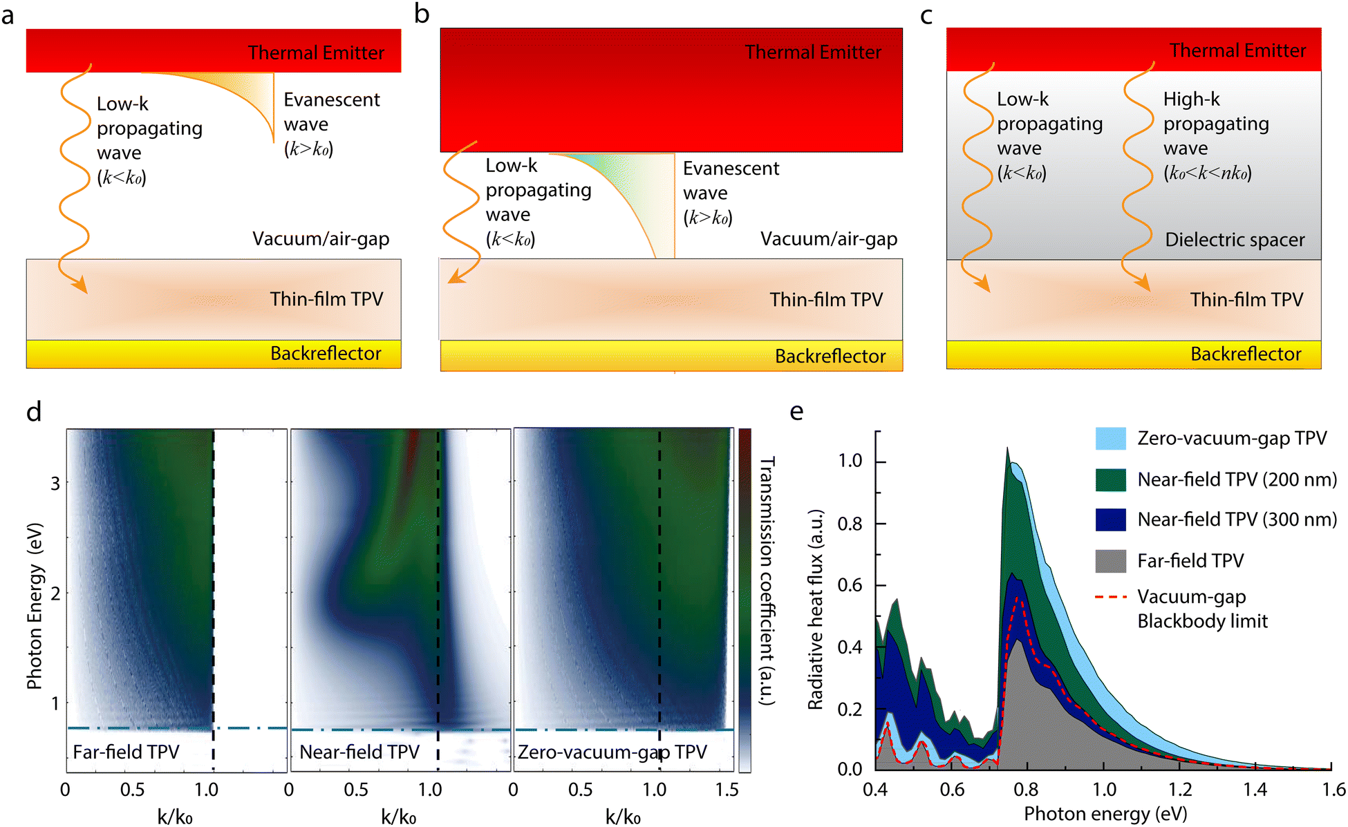 | ||
| Fig. 1 Principles of zero-vacuum-gap TPV (z-TPV) and conventional gap-integrated far-field TPV (f-TPV) and near-field TPV (n-TPV). Concepts of radiative energy flow are shown for far-field (a) and near-field (b) TPVs between a thermal emitter (graphite) and a low-bandgap PV cell (InGaAs), separated by a vacuum or an air gap. The macroscale gap in far-field TPV allows only the transmission of propagating waves with low parallel wavevectors (k < k0, k0 = ω/c, where ω is the photon frequency and c is the speed of light in a vacuum), while a nanoscale gap in near-field TPV allows the transmission of high-k photons via coupling of evanescent waves. (c) Concept of z-TPV in which a transparent, thermally insulating dielectric spacer is inserted between the emitter and the PV cell to turn vacuum-prohibited evanescent waves into high-k (k0 < k < nk0) propagating waves, where n is the refractive index of the spacer. (d) Calculated spectral thermal radiation transmission for different TPV schemes. a.u., arbitrary units. The emitter temperature is 1200 K. The gap size for near-field TPV is 300 nm. (e) Spectral heat flux of different TPV schemes. Fused quartz is used as the dielectric spacer. The thermal radiation energy density in far-field TPV using a blackbody emitter is calculated for comparison. The values are normalized by the maximum value of the z-TPV spectral radiative flux. | ||
Alternatively, zero-vacuum-gap TPV provides a different approach from near-field TPV to access the high-k waves which contain high thermal energy content for power generation.26,49 As shown in Fig. 1c, when a dielectric medium with a refractive index of n fills the gap, it opens an extra energy pathway for high-k propagating waves (k0 < k < nk0), which can be harvested to generate more power in the PV cell. It is important to note that the high-k waves here are propagating and not evanescent; therefore, there is no decay in intensity inside the transparent spacer layer. In this context, zero-vacuum-gap TPV can be considered as a variant of far-field TPV as there is no contribution from the near-field evanescent waves. However, the contribution of high-k propagating waves is substantial. Indeed, the calculated wave vector- and wavelength-dependent energy transmission coefficients (Fig. 1d; see the ESI† for the theoretical method) suggest that zero-vacuum-gap TPV allows a broadband enhancement in radiative heat flux beyond k0 while near-field TPV increases energy flux by enhancing transmission within a small interval of wavelengths and wave vectors.
In our calculations, fused quartz was used as an example of the dielectric spacer material due to its near-perfect transmittance in near-IR (0.5–2 μm), relatively high refractive index (n = 1.45), and low thermal conductivity (1.4 W m−1 K−1).50Fig. 1e shows the spectral power distribution of different TPV devices operated using a 0.74-eV InGaAs cell with an integrated Au back reflector. Both the near-field and zero-vacuum-gap TPV devices have the potential to beat the far-field blackbody limit for vacuum/air-gap TPV devices. Notably, the performance of zero-vacuum-gap TPV when using fused quartz as the dielectric spacer is comparable to that of a near-field TPV device with a vacuum gap of approximately 200 nm.
Furthermore, it is important to note that the presented zero-vacuum-gap TPV concept above shares similarities with a historical TPV approach known as light-pipe TPV,51–53 which also employs an intermediate spacer to enhance the power density of TPV devices (see the ESI† for details). However, all prior experimental demonstrations of light-pipe TPV featured an air gap between the emitter and the PV cell, fundamentally limiting the TPV power density to contributions only from low-k modes. While in theory, the light-pipe TPV concept could be adapted for a gapless structure, no experimental demonstrations have been reported to date. In this work, we clarify these two methods and use the term “zero-vacuum-gap TPV” to more accurately describe the architecture of this different concept.
Device fabrication and power enhancement demonstration
To demonstrate the experimental feasibility of zero-vacuum-gap TPV and its potential to break the vacuum-gap blackbody limit, we fabricated zero-vacuum-gap TPV devices and characterized their performance. Fig. 2 shows the schematic of the experimental setup. To fabricate this device, we first sputtered thick (>1 μm) emitter films (tungsten and graphite) on the end-polished fused quartz rods with a roughness of ∼1–5 nm. Subsequently, the fused quartz rods were attached to the PV cell using a very thin layer (∼10 μm) of an optical epoxy (EB-107LP-2FL) with a similar index as fused quartz to seal the air gap between the spacer layer and the grid line-covered PV cell surface. During our measurements, the emitter was heated using an electrical heater and the temperature of the emitter was monitored using three thin film thermocouples (K-type with a 25 μm probe). To ensure excellent thermal contact, a ceramic glue (Resbond 989F) was used to joint the heater rod and the thermal emitter as well as these thermocouples. The temperature of the PV cell was measured using two thermocouples glued using a thermally conductive, electrically non-conductive epoxy (H70E), with one positioned underneath and another located on the side of the cell. The heat flux flowing from the PV cell to the bottom heat sink was measured using a heat flux sensor (HFS) placed between the cell and the heat exchanger (M2 microchannel cold plate), secured with a thermal paste (Shin Etsu X23). To thermally insulate the device, two layers of thermal insulation were used on top of the heater and underneath the device. The photovoltaic cell used in our measurement is InGaAs with a bandgap Eg of 0.74 eV and is grown by metal–organic vapor phase epitaxy (see the ESI† and Fig. S2) which is a commonly used method to produce high quality, scalable III–V semiconductors in the commercial sector. Furthermore, to account for the view factor effect (see the ESI†) due to the small size of the PV cell (∼0.1 cm2), our measurements were performed by first bringing the PV cell ∼1 mm away from the combined spacer and emitter layers, to obtain the far-field TPV results, and then closing the gap using epoxy to characterize zero-vacuum-gap TPV cell performance using the same set of emitters and PV cells. By doing so, the ratio of power densities in two TPV methods can be obtained. It should be noted here that our far-field TPV measurements, intermediated with a transparent spacer but incorporating a thin air gap, are the same as the light-pipe far-field TPV (see the ESI†).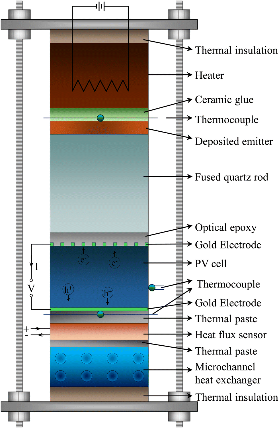 | ||
| Fig. 2 Schematics (not to scale) of the measurement setup. | ||
The measured power generation from gap-integrated far-field TPV and zero-vacuum-gap TPV for both tungsten and graphite emitters at varying temperatures are shown in Fig. 3a and d. We compared these results to our theoretical predictions as well as the vacuum-gap blackbody limits. For both emitters, zero-vacuum-gap TPV generates more power than the blackbody limit for a vacuum-gap far-field device. Specifically, the power performance is more pronounced for the graphite emitter (approximately 60% higher than the blackbody limit) since graphite has a higher emissivity54,55 compared to tungsten.56 Furthermore, as shown in Fig. 3b and e, for both emitters, we observed that adopting the zero-vacuum-gap architecture improves the TPV power density by a factor of two. The similar enhancement ratio for two different emitters suggests that the zero-vacuum-gap architecture can be used as a universal approach to elevate the power output of existing far-field TPV cells. It should be noted that the power enhancement is less than the prediction of the upper limit of the enhancement ratio which is around 2.65 for the fused quartz spacer and is approximately independent of the emitter temperature. This can be attributed to several energy loss mechanisms and the non-ideal device configuration used in our measurement (see the ESI†). The current–voltage characteristics (J–V) of both the zero-vacuum-gap and far-field TPV cells are measured using a four-wire method to obtain Pmax = IscVocFF, where Isc is the short-circuit current, Voc is the open-circuit voltage, and FF is the fill factor (see the ESI† and Fig. S4). As shown in Fig. 3c and f, it is found that zero-vacuum-gap TPV at lower emitter temperatures can generate higher current densities than far-field TPV, even in the presence of energy losses. This highlights the potential of zero-vacuum-gap TPV to relax the high temperature requirements in current TPV devices as achieving equivalent power output density at lower emitter temperatures is of great importance for many TPV applications with material and temperature constraints.
 | ||
| Fig. 3 Measured power density and current–voltage characteristics in zero-vacuum-gap and far-field TPVs using tungsten and graphite as thermal emitters. (a) and (d) Measured and calculated power density of zero-vacuum-gap and far-field TPV devices at different emitter temperatures. The red shaded area represents the uncertainty of calculated power due to various energy losses. (b) and (e) Power enhancement ratio between the measured zero-vacuum-gap and far-field TPV devices for graphite and tungsten emitters, respectively. (c) and (f) J–V characteristics of zero-vacuum-gap and far-field TPV devices at different temperatures. | ||
The power density of TPV devices is a function of several physical factors, including the emitter temperature, view factor between the cell and the emitter, and the area and emissivity of both the emitter and PV cell. It is important to note that unlike efficiency, which can be compared across different experimental configurations with minimal adjustments, extra care is required when comparing reported values of power density. Here, we adopt the concept of the power density figure of merit proposed by Giteau et al.57 and use two dimensionless power densities (Pn1 and Pn2) based on two different normalization factors to enable fair comparisons among various TPV schemes reported in the literature. Pn1 and Pn2 are expressed as
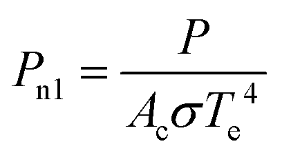 | (1) |
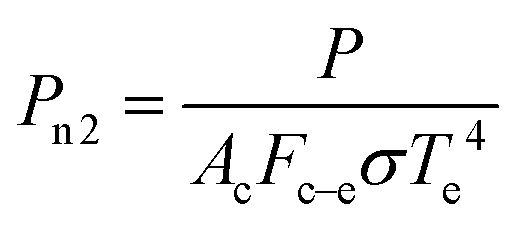 | (2) |
As shown in Fig. 4, the performance of zero-vacuum-gap TPV, evaluated using both normalization metrics, is among the highest reported power densities at moderate working temperatures (700–1100 °C) when compared to high-performance far-field TPV devices demonstrated over the past two decades using PV cells with a similar bandgap (∼0.7 eV). Furthermore, our measured power density using conventional far-field design with our PV cells is relatively low compared to nearly all reported results, reflecting the fact that the PV cells in our measurement are not optimized and exhibit significant losses (i.e., high series resistance, as discussed below). However, the adoption of the zero-vacuum-gap TPV design significantly improved performance.
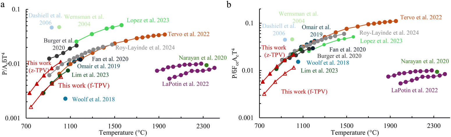 | ||
| Fig. 4 Comparison of power density between zero-vacuum-gap TPV and other reported far-field TPV devices. Dimensionless power density ((a) with and (b) without considering the view factor) as a function of the emitter temperature is used to compare the TPV power densities reported in the literature including Burger et al.,14 Tervo et al.,30 Roy-Layinde et al.,32 Fan et al.,29 Omair et al.,31 Lim et al.,35 Woolf et al.,58 Narayam et al.,34 Lopez et al.,33 Wernsman et al.,59 Dashiell et al.60 and LaPotin et al.28 | ||
As both zero-vacuum-gap and near-field TPV are promising methods to achieve high power densities at moderate temperatures, we compare their power densities in Fig. 5. As shown in Fig. 5a, z-TPV achieves a power density comparable to the best of near-field TPVs reported in the literature. Notably, the PV cell used in both our work and in the study by Mittapally et al.48 is InGaAs, allowing for a detailed comparison. We specifically compare the enhancement ratio of zero-vacuum-gap TPV with that of near-field TPV, as reported by Mittapally et al.,48 at different nanogap sizes. As shown, zero-vacuum-gap TPV with fused quartz as the spacer achieves a similar enhancement ratio to near-field TPV with a vacuum gap between 200 and 250 nm. We also performed the simulation for near-field TPV using the same emitter and PV cell as in our zero-vacuum-gap TPV experiment and found that the power performance of our fabricated device matches that of the near-field device at the same temperature with a vacuum gap of 175 nm (see the ESI†). Given that both methods can achieve high power densities at moderate temperatures, our results suggest that zero-vacuum-gap TPV devices could overcome the scalability challenges faced by near-field TPV, enabling high power output for large-scale applications.
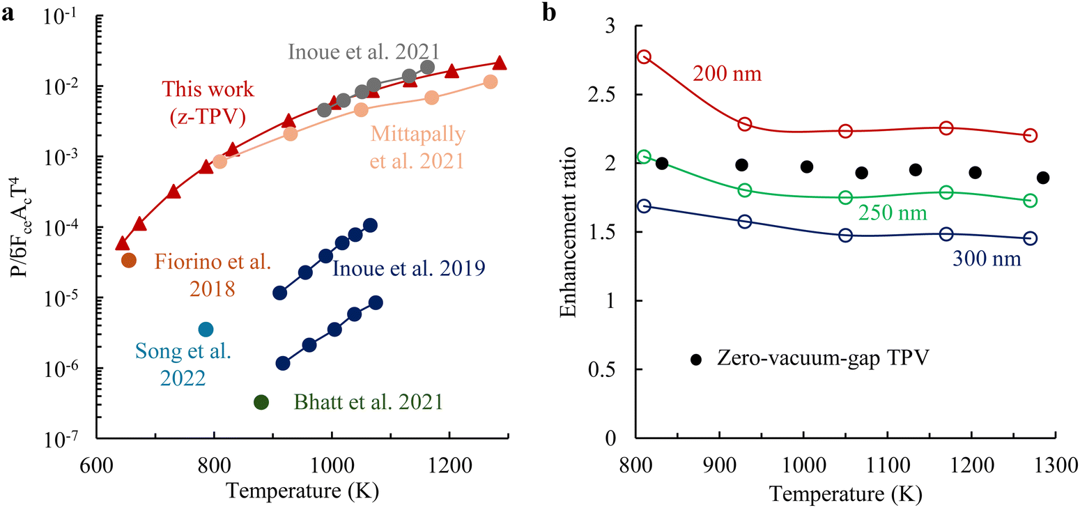 | ||
| Fig. 5 Comparison between zero-vacuum-gap TPV and near-field TPV devices. (a) The normalized power generation density as a function of the emitter temperature is used to compare the zero-vacuum-gap TPV with near-field TPV in recent experiments including Mittapally et al.,48 Inoue et al.,61 Fiorino et al.,46 Inoue et al.,62 Song et al.,63 and Bhatt et al.64 The gap sizes of 50 nm and 350 nm were selected for the works by Fiorino et al.46 and Mittapally et al.48 (b) The comparison between the enhancement ratio of the zero-vacuum-gap TPV and near-field TPV of Mittapally et al.48 work. Three different gap sizes of 200, 250, and 300 nm are selected. The PV cell in both experiments is InGaAs. | ||
Efficiency characterization and effects of heat conduction
One of the limitations of zero-vacuum-gap TPV devices is the heat conduction through the dielectric spacer layer, which causes energy loss and may lead to unwanted heating of the PV cell. It is important to note here that the device configuration of z-TPV is similar to that of thermoelectric devices, where heat conduction through the semiconductor materials needs to be accounted for in device design and minimized to reach high efficiency.65 However, z-TPV has the advantage of using any low thermal conductivity, thermally insulating materials as the intermediate layer (e.g., fused quartz and amorphous silicon), which are not constrained by the semiconductor materials in thermoelectrics.The figure of merit we used to evaluate zero-vacuum-gap TPV is the efficiency on the PV cell side (i.e., cell energy conversion efficiency), η = Pgen/(Qrad + Qcond), where Pgen is the generated power from the PV cell and Qrad and Qcond are the heat radiation and conduction that reach the PV cell which are measured using a heat flux sensor underneath the cell. Fig. 6a shows the measured efficiency of our zero-vacuum-gap devices for the fused quartz spacer with different lengths. See the ESI† for details about the efficiency measurement. For a 2-cm long dielectric spacer, the efficiency is low (less than 5% at 1290 K) due to the dominant role of heat conduction. However, increasing the dielectric spacer to 10 cm significantly suppresses the conduction contribution and improves the efficiency to nearly 19%. It should be noted that although the power density in zero-vacuum-gap TPV is enhanced by a factor of 2 compared to conventional far-field TPV, the measured efficiencies of both TPV architectures are comparable. This is because zero-vacuum-gap TPV increases power generation by extracting a proportionally similar additional amount of thermal radiation from the emitter, primarily through the high-k modes. Furthermore, efficiency improves as the emitter temperature increases, which can be explained by the improved spectral matching between the thermal emission spectrum and the PV cell bandgap, as well as the significant rise in radiative power, which increases at a higher rate (∼T4) compared to conductive heat transfer (∼T). As shown in Fig. S7 (ESI†), thermal radiation dominates over the contributing heat conduction in the total heat flux at above 1200 K for the fused quartz spacer.
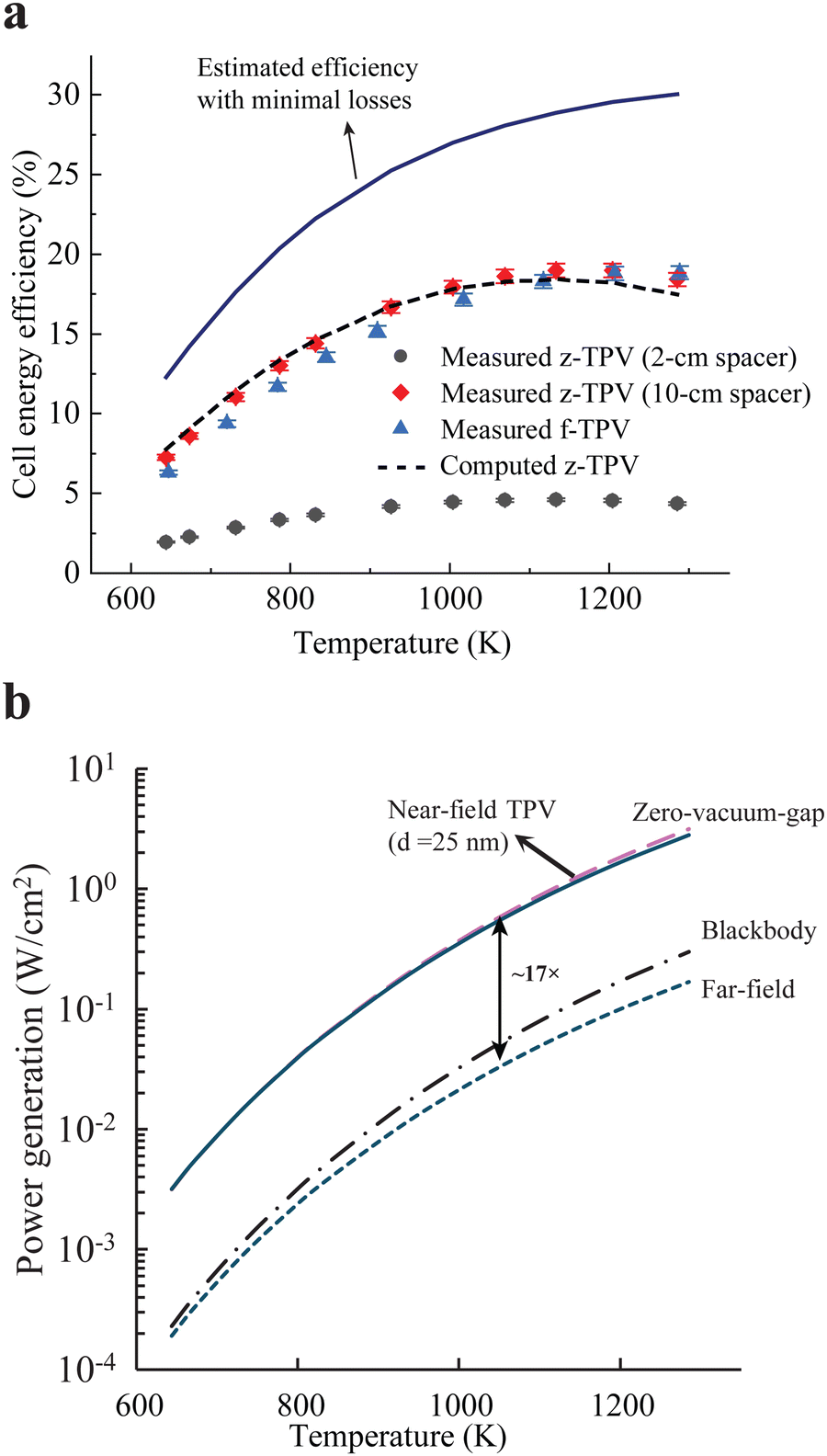 | ||
| Fig. 6 Measured and calculated cell energy conversion efficiency and predicted performance using other dielectric spacer materials for achieving even higher power density (all calculations assumed graphite as the thermal emitter). (a) Measured and calculated efficiency of far-field TPV and zero-vacuum-gap TPV (with fused quartz spacer thicknesses of 2 and 10 cm) at different temperatures. The optimal efficiency for different TPV schemes is calculated using optimized PV cell parameters extracted from the recently demonstrated high efficiency InGaAs cell with minimal optoelectronic losses. The vacuum gap size in near-field TPV is 200 nm. The spacer thickness for modelling zero-vacuum-gap TPV is 10 cm. (b) Estimated power density of zero-vacuum-gap TPV using amorphous-Si as the dielectric spacer material and compared with the far-field TPV. The dashed red line between a-Si corresponds to near-field TPV with a gap size of 25 nm. | ||
Furthermore, we have performed characterization of the PV cell temperature, and our experiments suggest that the heating of the PV cell due to both radiative absorption and conduction has marginal adverse effects on the TPV power performance (see the ESI† and Fig. S8).
The measured efficiency of zero-vacuum-gap TPV agrees well with our theoretical calculations when accounting for several loss mechanisms, such as series resistance (see the ESI†). It is worth noting that a recent experiment by some of us using a similar type of InGaAs cell that has much lower series resistance and reported nearly 40% efficiency by effectively minimizing losses.30 However, even in that study, the efficiency decreases to around 25% when the emitter temperature reduces to 1000 °C.
To optimize the power density and efficiency of the z-TPV devices, it is critical to manage the energy losses, including radiation escaping due to light traveling in an oblique angle and leaving the side surface of the spacer, optical losses inside the spacer, energy transmission losses of the high-k modes, heat conduction and convection losses, and optoelectronic losses inside the PV cell. According to our estimation, the escaped radiation and optical losses in the fused quartz dominate in our current devices as fused quartz has a modest refraction index (thus a higher percentage of light leaving the side wall without undergoing total internal reflection). However, several methods can be adopted to optimize efficiency while maintaining the high-power density, including using an alternative dielectric spacer with a higher refractive index, or using a cylinder shape TPV device (see the ESI†). Furthermore, the heat transfer losses in the z-TPV structure can be managed by using a spacer material that has low thermal conductivity and using a device shape that is more immune to an external thermal environment such as a cylindrical TPV device used in many TPV applications such as a fuel-combustion power generator and grid energy storage. In addition, reducing the optoelectronic losses in the PV cell due to high series resistance is critical to further improve the efficiency of z-TPV devices. Moreover, to improve the efficiency at medium temperatures, a PV cell with a bandgap below 0.7 eV should be used to have a better spectral match with the thermal radiation spectrum. We expect that the same optimization in PV cell fabrication and using a low band-gap PV cell can be employed to improve the efficiency of the current zero-vacuum-gap TPV devices. Indeed, using the physical parameters derived from the optimized InGaAs cells, we found that a possible upper efficiency value for zero-vacuum-gap TPV could reach around 30% at 1200 K (Fig. 6a). These results indicate that zero-vacuum-gap TPV does not inherently come with compromised efficiency due to the existence of thermal losses. Furthermore, it is also important to note that the cell energy efficiency reported here does not account for the transmission optical losses because of the sub-bandgap photon absorption in the dielectric spacer. As a proof-of-concept demonstration, we chose fused quartz due to its low cost and simple integration into the z-TPV architecture. The near-transparent transmission band of fused quartz is in the near infrared (0.5–2 μm). This is great for demonstrating the power enhancement mechanism of zero-vacuum-gap TPV as we are using a 0.74 eV cell, meaning most of the above-bandgap thermal radiation photons from the emitters can be used to enhance power generation. However, the optical losses due to the non-transparent below-bandgap photons of the fused quartz are also important for practical implementations of z-TPV as they limit the overall efficiency of the device. These photons do not contribute to power generation and are instead converted to heat. For fused quartz and the PV cell used in this work, this loss is more than half of the incoming radiation. However, this loss can be mitigated by using other mechanisms such as the selective emitter, the embedded structure on the emitter as an optical filter, or using alternative dielectric spacer materials with broad spectral infrared transparency to improve the overall efficiency of the system.
Theoretical potential of zero-vacuum-gap TPV
To obtain further insights into our results and answer the question of whether even higher power densities could be achieved using zero-vacuum-gap TPV, we performed theoretical predictions with other spacer materials. See the ESI† for details on our consideration of different materials. Specifically, we considered amorphous silicon (a-Si) due to its high refractive indices (>3), high infrared transparency, and low thermal conductivity (a-Si66 is close to fused quartz67). As shown in Fig. 6b, a-Si establishes a 17-fold higher power enhancement when compared with the far-field TPV devices using the same emitter and the PV cell. This high-power level is equivalent to that of near-field TPV for a <30-nm vacuum gap, which is nearly impossible to achieve using current microfabrication techniques. Furthermore, the power output of a far-field TPV device at 1000 °C can be reached using a zero-vacuum-gap architecture at only 650 °C if a-Si is used as the dielectric spacer, suggesting the potential of zero-vacuum-gap TPV for harvesting low-to-moderate quality heat that can be found in many heavy-emission industrial processes.Conclusions
We presented here the first demonstration of a novel zero-vacuum-gap TPV architecture that is different from existing far-field and near-field devices and showcased its power enhancement capability using a fused quartz dielectric spacer. It is anticipated that this method, once optimized, can elevate TPV power density to levels unattainable by both conventional far-field and near-field TPV devices. Our experiments showed the enhancement of TPV power density that could exceed the blackbody limit in air-gap far-field devices. Furthermore, given the potential for high-power density in zero-vacuum-gap TPV and compatibility with the scalable manufacturing methods, this method overcomes the dilemma facing the near-field TPV devices of the tradeoff between high power density and scalability. Our calculations further suggested that by properly choosing the spacer material in combination with PV cells that have been recently demonstrated with minimal thermal and optical losses, even higher power density can be achieved. The advances gained in this work set the stage to systematically investigate the zero-vacuum-gap concept and potentially unlock a wide range of low-to-moderate temperature heat sources that have not been exploited in many TPV energy conversion applications such as lightweight heat power co-generators, and concentrated solar TPV paired with moderate temperature thermal storage systems.Author contributions
This work was conceived by L. C. The TPV devices were fabricated by M. H., S. Y., and Y. Z. The experiments were performed by M. H. and S. Y. The InGaAs cells were fabricated and characterized by E. J. T. and M. A. S. The calculations were performed by M. H. and L. C. The manuscript was written by M. H. and L. C. with the input from all authors.Data availability
The data supporting this article have been included as part of the ESI.† Other findings of this study and data plots are available from the corresponding author upon reasonable request.Conflicts of interest
L. C. and M. H. have a pending patent application (PCT/US2023/020336) related to work described here.Acknowledgements
L. C. acknowledges support from the National Science Foundation (No. 2239004 and 2343027), the NSF I-Corps program (No. 2311324), the Colorado Office of Economic Development and International Trade (OEDIT DO 2024-2320), and the Lab Venture Challenge Prize and Research & Innovation Office Seed Grant at CU Boulder. E. T. acknowledges support from the NSF (No. 2343028) and the Laboratory Directed Research and Development (LDRD) Program at the National Renewable Energy Laboratory (NREL). This work was authored in part by the NREL, operated by Alliance for Sustainable Energy, LLC, for the U. S. Department of Energy (DOE) under contract no. DE-AC36-08GO28308. This work utilized resources from the University of Colorado Boulder Research Computing, which is supported by the National Science Foundation (ACI-1532235 and ACI-1532236), University of Colorado Boulder, and Colorado State University.References
- A. Datas and R. Vaillon, Thermophotovoltaic energy conversion, Ultra-High Temperature Thermal Energy Storage, Transfer and Conversion, 2021, pp. 285–308 Search PubMed.
- H. Daneshvar, R. Prinja and N. P. Kherani, Thermophotovoltaics: Fundamentals, challenges and prospects, Appl. Energy, 2015, 159, 560–575 CrossRef.
- T. Burger, C. Sempere, B. Roy-Layinde and A. Lenert, Present Efficiencies and Future Opportunities in Thermophotovoltaics, Joule, 2020, 4, 1660–1680 CrossRef.
- A. Licht, N. Pfiester, D. DeMeo, J. Chivers and T. E. Vandervelde, A Review of Advances in Thermophotovoltaics for Power Generation and Waste Heat Harvesting, MRS Adv., 2019, 4, 2271–2282 CrossRef.
- Z. Utlu and U. Parali, Investigation of the potential of thermophotovoltaic heat recovery for the Turkish industrial sector, Energy Convers. Manage., 2013, 74, 308–322 CrossRef.
- A. Veeraragavan, L. Montgomery and A. Datas, Night time performance of a storage integrated solar thermophotovoltaic (SISTPV) system, Sol. Energy, 2014, 108, 377–389 CrossRef.
- H. Wu, M. Kaviany and O. C. Kwon, Thermophotovoltaic power conversion using a superadiabatic radiant burner, Appl. Energy, 2018, 209, 392–399 CrossRef.
- A. S. Rana, et al., Broadband solar absorption by chromium metasurface for highly efficient solar thermophotovoltaic systems, Renewable Sustainable Energy Rev., 2023, 171, 113005 CrossRef.
- A. Schock, M. Mukunda, C. Or, V. Kumar and G. Summers, Design, analysis, and optimization of a radioisotope thermophotovoltaic (RTPV) generator, and its applicability to an illustrative space mission, Acta Astronaut., 1995, 37, 21–57 CrossRef.
- K. F. Mustafa, S. Abdullah, M. Z. Abdullah and K. Sopian, A review of combustion-driven thermoelectric (TE) and thermophotovoltaic (TPV) power systems, Renewable Sustainable Energy Rev., 2017, 71, 572–584 CrossRef.
- V. L. Teofilo, P. Choong, J. Chang, Y. L. Tseng and S. Ermer, Thermophotovoltaic energy conversion for space, J. Phys. Chem. C, 2008, 112, 7841–7845 CrossRef.
- L. M. Fraas, J. E. Avery and H. X. Huang, Thermophotovoltaic furnace–generator for the home using low bandgap GaSb cells, Semicond. Sci. Technol., 2003, 18, S247 CrossRef.
- H. Reza Seyf and A. Henry, Thermophotovoltaics: a potential pathway to high efficiency concentrated solar power, Energy Environ. Sci., 2016, 9, 2654–2665 RSC.
- T. Burger, et al., Semitransparent thermophotovoltaics for efficient utilization of moderate temperature thermal radiation, Proc. Natl. Acad. Sci. U. S. A., 2022, 119, e2215977119 CrossRef PubMed.
- B. Zhao, et al., High-performance near-field thermophotovoltaics for waste heat recovery, Nano Energy, 2017, 41, 344–350 CrossRef.
- R. Bhatt, I. Kravchenko and M. Gupta, High-efficiency solar thermophotovoltaic system using a nanostructure-based selective emitter, Sol. Energy, 2020, 197, 538–545 CrossRef.
- Y. Wang, H. Liu and J. Zhu, Solar thermophotovoltaics: Progress, challenges, and opportunities, APL Mater., 2019, 7, 80906 CrossRef.
- Z. Zhou, E. Sakr, Y. Sun and P. Bermel, Solar thermophotovoltaics: Reshaping the solar spectrum, Nanophotonics, 2016, 5, 1–21 Search PubMed.
- N. P. Harder and P. Würfel, Theoretical limits of thermophotovoltaic solar energy conversion, Semicond. Sci. Technol., 2003, 18, S151 CrossRef.
- A. Lenert, et al., A nanophotonic solar thermophotovoltaic device, Nat. Nanotechnol., 2014, 9, 126–130 CrossRef PubMed.
- D. M. Bierman, et al., Enhanced photovoltaic energy conversion using thermally based spectral shaping, Nat. Energy, 2016, 1, 1–7 Search PubMed.
- C. Amy, H. R. Seyf, M. A. Steiner, D. J. Friedman and A. Henry, Thermal energy grid storage using multi-junction photovoltaics, Energy Environ. Sci., 2019, 12, 334–343 RSC.
- A. Datas, A. Ramos, A. Martí, C. del Cañizo and A. Luque, Ultra high temperature latent heat energy storage and thermophotovoltaic energy conversion, Energy, 2016, 107, 542–549 CrossRef.
- A. Datas, A. López-Ceballos, E. López, A. Ramos and C. del Cañizo, Latent heat thermophotovoltaic batteries, Joule, 2022, 6, 418–443 CrossRef.
- M. Bianchi, C. Ferrari, F. Melino and A. Peretto, Feasibility study of a Thermo-Photo-Voltaic system for CHP application in residential buildings, Appl. Energy, 2012, 97, 704–713 CrossRef.
- M. Habibi and L. Cui, Modelling and performance analysis of a novel thermophotovoltaic system with enhanced radiative heat transfer for combined heat and power generation, Appl. Energy, 2023, 343, 121221 CrossRef.
- E. López, I. Artacho and A. Datas, Thermophotovoltaic conversion efficiency measurement at high view factors, Sol. Energy Mater. Sol. Cells, 2023, 250, 112069 CrossRef.
- A. LaPotin, et al., Thermophotovoltaic efficiency of 40%, Nature, 2022, 604, 287–291 CrossRef PubMed.
- D. Fan, et al., Near-perfect photon utilization in an air-bridge thermophotovoltaic cell, Nature, 2020, 586, 237–241 CrossRef PubMed.
- E. J. Tervo, et al., Efficient and scalable GaInAs thermophotovoltaic devices, Joule, 2022, 6, 2566–2584 CrossRef.
- Z. Omair, et al., Ultraefficient thermophotovoltaic power conversion by band-edge spectral filtering, Proc. Natl. Acad. Sci. U. S. A., 2019, 116, 15356–15361 CrossRef PubMed.
- B. Roy-Layinde, J. Lim, C. Arneson, S. R. Forrest and A. Lenert, High-efficiency air-bridge thermophotovoltaic cells, Joule, 2024, 8, 1–11 CrossRef.
- E. López, I. Artacho and A. Datas, Thermophotovoltaic conversion efficiency measurement at high view factors, Sol. Energy Mater. Sol. Cells, 2023, 250, 112069 CrossRef.
- T. C. Narayan, et al., World record demonstration of >30% thermophotovoltaic conversion efficiency, Conference Record of the IEEE Photovoltaic Specialists Conference 2020-June, 2020, pp. 1792–1795.
- J. Lim, B. Roy-Layinde, B. Liu, A. Lenert and S. R. Forrest, Enhanced Photon Utilization in Single Cavity Mode Air-Bridge Thermophotovoltaic Cells, ACS Energy Lett., 2023, 8, 2935–2939 CrossRef.
- G. Vaidhyanathan Krishnamurthy, et al., Iridium-Based Selective Emitters for Thermophotovoltaic Applications, Adv. Mater., 2023, 35, 2305922 CrossRef PubMed.
- R. Sakakibara, et al., Practical emitters for thermophotovoltaics: a review, J. Photonics Energy, 2019, 9, 032713 Search PubMed.
- M. R. S. Dias, et al., Photonics roadmap for ultra-high-temperature thermophotovoltaics, Joule, 2023, 7, 2209–2227 CrossRef.
- R. Mittapally, A. Majumder, P. Reddy and E. Meyhofer, Near-Field Thermophotovoltaic Energy Conversion: Progress and Opportunities, Phys. Rev. Appl., 2023, 10, 37002 CrossRef.
- G. T. Papadakis, S. Buddhiraju, Z. Zhao, B. Zhao and S. Fan, Broadening Near-Field Emission for Performance Enhancement in Thermophotovoltaics, Nano Lett., 2020, 20, 1654–1661 CrossRef.
- M. Laroche, R. Carminati and J. J. Greffet, Near-field thermophotovoltaic energy conversion, J. Appl. Phys., 2006, 100, 63704 CrossRef.
- A. Narayanaswamy and G. Chen, Surface modes for near field thermophotovoltaics, Appl. Phys. Lett., 2003, 82, 3544–3546 CrossRef.
- J. Song, J. Han, M. Choi and B. J. Lee, Modeling and experiments of near-field thermophotovoltaic conversion: A review, Sol. Energy Mater. Sol. Cells, 2022, 238, 111556 CrossRef.
- G. R. Bhatt, et al., Integrated near-field thermo-photovoltaics for heat recycling, Nat. Commun., 2020, 11, 1–7 CrossRef PubMed.
- C. Lucchesi, et al., Near-Field Thermophotovoltaic Conversion with High Electrical Power Density and Cell Efficiency above 14%, Nano Lett., 2021, 21, 4524–4529 CrossRef.
- A. Fiorino, et al., Nanogap near-field thermophotovoltaics, Nat. Nanotechnol., 2018, 13, 806–811 CrossRef PubMed.
- T. Inoue, et al., One-Chip Near-Field Thermophotovoltaic Device Integrating a Thin-Film Thermal Emitter and Photovoltaic Cell, Nano Lett., 2019, 19, 3948–3952 CrossRef PubMed.
- R. Mittapally, et al., Near-field thermophotovoltaics for efficient heat to electricity conversion at high power density, Nat. Commun., 2021, 12, 4364 CrossRef.
- M. S. Mirmoosa, S. A. Biehs and C. R. Simovski, Super-Planckian Thermophotovoltaics Without Vacuum Gaps, Phys. Rev. Appl., 2017, 8, 054020 CrossRef.
- W. L. Shackleford, C. D. Bass and E. C. Beder, Transmissivity and Absorption of Fused Quartz Between 0.22 μ and 3.5 μ from Room Temperature to 1500 °C, Appl. Opt., 1971, 10, 2263–2268 CrossRef PubMed.
- M. K. Goldstein, L. G. DeShazer, A. S. Kushch and S. M. Skinner, Superemissive light pipe for TPV applications, AIP Conf. Proc., 1997, 401, 315–326 Search PubMed.
- T. Bauer, I. Forbes, R. Penlington and N. Pearsall, Heat transfer modelling in thermophotovoltaic cavities using glass media, Sol. Energy Mater. Sol. Cells, 2005, 88, 257–268 CrossRef.
- D. L. Chubb, Light Pipe Thermophotovoltaics (LTPV), AIP Conf. Proc., 2007, 890, 297–316 CrossRef.
- L. Biasetto, M. Manzolaro and A. Andrighetto, Emissivity measurements of opaque gray bodies up to 2000 °C by a dual-frequency pyrometer, Eur. Phys. J. A, 2008, 38, 167–171 CrossRef.
- A. Maturilli, J. Helbert, S. Ferrari, B. Davidsson and M. D’Amore, Characterization of asteroid analogues by means of emission and reflectance spectroscopy in the 1- to 100-μm spectral range Science of solar system materials examined from Hayabusa and future missions (II) 7. Planetary science, Earth, Planets Space, 2016, 68, 1–11 CrossRef.
- P. Bermel, et al., Design and global optimization of high-efficiency thermophotovoltaic systems, Opt. Express, 2010, 3, A314 CrossRef PubMed.
- M. Giteau, M. F. Picardi and G. T. Papadakis, Thermodynamic figure of merit for thermophotovoltaics, J. Photonics Energy, 2024, 14, 042402 Search PubMed.
- D. N. Woolf, et al., High-efficiency thermophotovoltaic energy conversion enabled by a metamaterial selective emitter, Optica, 2018, 5, 213–218 CrossRef.
- B. Wernsman, et al., Greater than 20% radiant heat conversion efficiency of a thermophotovoltaic radiator/module system using reflective spectral control, IEEE Trans. Electron Devices, 2004, 51, 512–515 CrossRef.
- M. W. Dashiell, et al., Quaternary InGaAsSb thermophotovoltaic diodes, IEEE Trans. Electron Devices, 2006, 53, 2879–2888 Search PubMed.
- T. Inoue, et al., Integrated Near-Field Thermophotovoltaic Device Overcoming Blackbody Limit, ACS Photonics, 2021, 8, 2466–2472 CrossRef.
- T. Inoue, et al., One-Chip Near-Field Thermophotovoltaic Device Integrating a Thin-Film Thermal Emitter and Photovoltaic Cell, Nano Lett., 2019, 19, 3948–3952 CrossRef PubMed.
- J. Song, et al., Thermophotovoltaic Energy Conversion in Far-to-Near-Field Transition Regime, ACS Photonics, 2022, 9, 1748–1756 CrossRef.
- G. R. Bhatt, et al., Integrated near-field thermo-photovoltaics for heat recycling, Nat. Commun., 2020, 11, 1–7 CrossRef.
- S. Twaha, J. Zhu, Y. Yan and B. Li, A comprehensive review of thermoelectric technology: Materials, applications, modelling and performance improvement, Renewable Sustainable Energy Rev., 2016, 65, 698–726 CrossRef.
- H. Wada and T. Kamijoh, Thermal conductivity of amorphous silicon, Jpn. J. Appl. Phys., Part 2, 1996, 35, L648 CrossRef.
- I. M. Abdulagatov, et al., Thermal conductivity of fused quartz and quartz ceramic at high temperatures and high pressures, J. Phys. Chem. Solids, 2000, 61, 779–787 CrossRef.
Footnotes |
| † Electronic supplementary information (ESI) available. See DOI: https://doi.org/10.1039/d4ee04604h |
| ‡ These authors contributed equally. |
| This journal is © The Royal Society of Chemistry 2025 |