
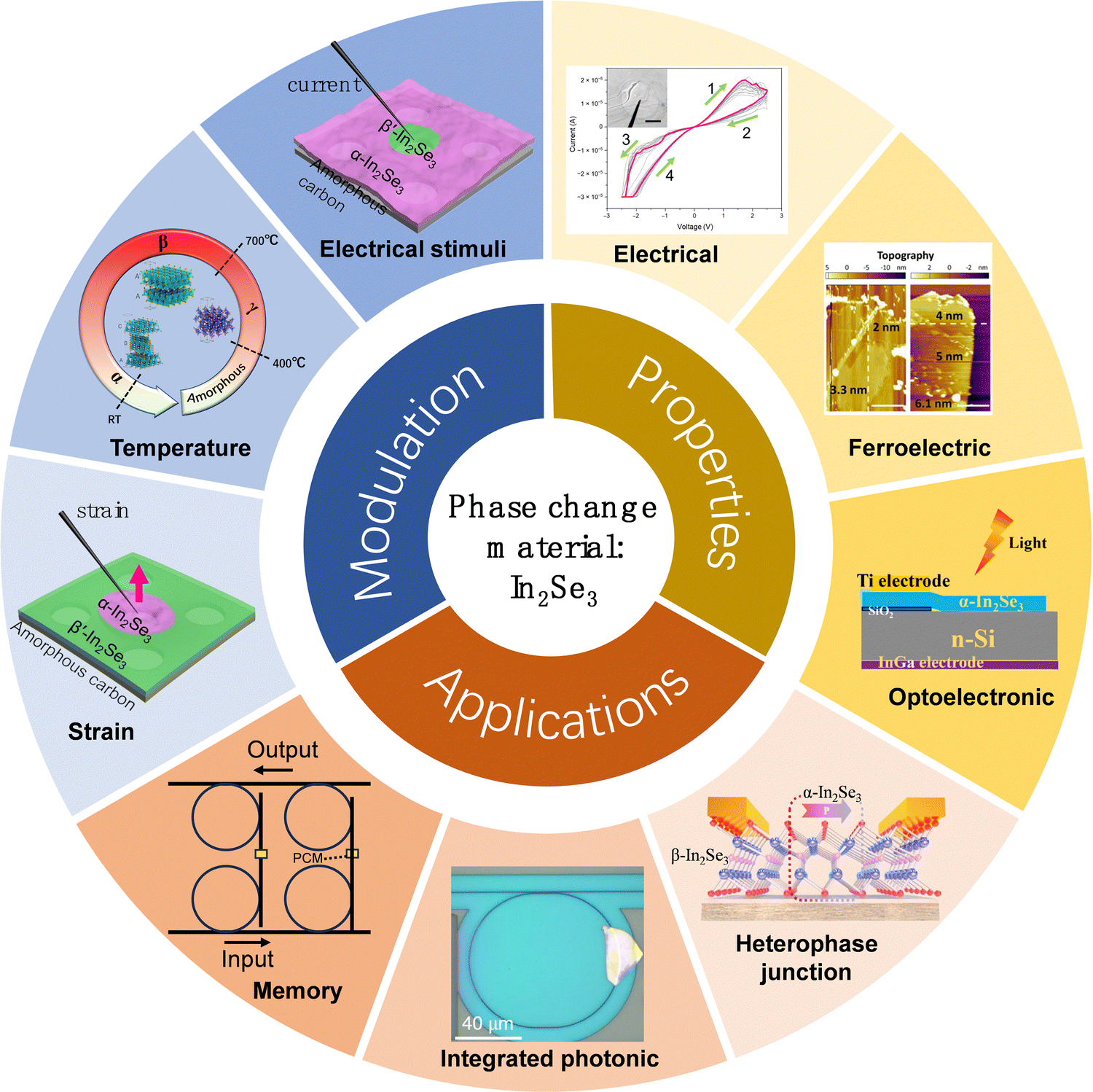
Polymorphic phases in 2D In2Se3: fundamental properties, phase transition modulation methodologies and advanced applications
Weiying Zhenga,
Zhiquan Liua,
Guoqiang Xia,
Tengzhang Liua,
Dingguan Wanga,
Lin Wangb and
Wugang Liao *a
*a
aState Key Laboratory of Radio Frequency Heterogeneous Integration (Shenzhen University), College of Electronics and Information Engineering, Shenzhen 518060, China. E-mail: wgliao@szu.edu.cn
bSchool of Mechanical Engineering, Shanghai Jiao Tong University, Shanghai 200240, People's Republic of China
First published on 9th April 2025
Abstract
Two-dimensional (2D) In2Se3, which is a multifunctional semiconductor, exhibits multiple crystallographic phases, each of which possesses distinct electronic, optical, and thermal properties. This inherent phase variability makes it a promising candidate for a wide range of applications, including memory devices, photovoltaics, and photodetectors. This review comprehensively explores the latest progress of various polymorphic phases of 2D In2Se3, emphasizing their unique properties, characterization methods, phase modulation strategies, and practical applications. Commencing with a rigorous examination of the structural attributes inherent in its various phases, we introduce sophisticated techniques for its characterization. Subsequently, modulation strategies, encompassing variations in temperature, application of electric fields, induced stress, and alterations in pressure, are explored, each exerting an influence on the phase transitions in 2D In2Se3. Finally, we highlight recent advancements and applications resulting from these phase transitions, including homoepitaxial heterophase structures, optical modulators, and phase change memory (PCM). By synthesizing insights into phase properties, modulation strategies, and potential applications, this review endeavours to provide a comprehensive understanding of the significance and prospects of In2Se3 in the semiconductor field.
1. Introduction
The rapid advancement of semiconductor technology has led to an increasing demand for materials with superior performance characteristics. To meet the needs of efficient, low-power, and highly integrated devices, two-dimensional (2D) materials have garnered significant attention due to their unique electronic structures and exceptional physical properties.1 Their ultrathin structure reduces electron interference during movement, resulting in higher electron mobility and lower energy consumption.2–7 Additionally, 2D materials exhibit outstanding mechanical flexibility,8–11 optical transparency,12–15 and chemical stability,16–19 opening up new opportunities for innovative semiconductor device designs. Among the various 2D materials, In2Se3 stands out by virtue of its unique phase transition behavior.16,20–30 As a multifunctional semiconductor, In2Se3 can exist in multiple crystalline phases, including the well-established phases (α, β, and γ), as well as less common phases (α′, β′, β′′, γ′, δ, and κ). Each phase exhibits distinct electronic, optical, and thermal properties.31–37 Notably, the ferroic properties of certain phases, such as α and β′ phases, have been applied in ultra-fast memory and neuromorphic computing.38–41 The ability to modulate these phases offers significant advantages for tailoring In2Se3's properties to specific applications.This diverse phase behavior not only broadens the potential applications of In2Se3 but also underscores the complexity and dynamic nature of semiconductor materials.42 The phase transition behavior of In2Se3 enables dynamic control of its performance in response to external stimuli like temperature, electric fields, stress, and pressure.35,43–48 Under these conditions, the material undergoes reversible transitions between different crystal structures, making it a tunable platform for controlling the electronic and optical properties. This dynamic behavior is particularly useful in applications ranging from memory devices to photodetectors. For example, manipulating In2Se3's phase transitions can facilitate rapid writing and erasing in memory devices, improve photoelectric conversion efficiency in photovoltaic cells, and optimize the response speed and sensitivity of photodetectors.29
Moreover, the 2D structure of In2Se3 allows for the formation of heterostructures with other 2D materials, further expanding its potential in semiconductor devices.49–51 From memory devices to photovoltaic and photodetectors, the phase change behavior of In2Se3 offers unique opportunities for novel devices.20,52–54 Therefore, 2D In2Se3's remarkable phase-change characteristics represent a significant advancement in semiconductor technology. Understanding its phase transitions not only enhances our knowledge of the underlying physics and chemistry of semiconductor materials, but also provides insights into the development of novel materials and device designs for future applications. With its wide-ranging applications and potential for innovation, In2Se3 continues to be a promising material for ongoing research and development in the semiconductor field.31,55–62
This review examines the intricate phase transitions of In2Se3, which are central to its material science and semiconductor applications. We explore the distinct structures of its various phases, particularly the three most common polymorphs (α, β, and γ), and highlight how their unique properties contribute to In2Se3's versatility. Despite significant efforts to synthesize and study its phases,63,64 there is still a lack of comprehensive reviews summarizing the developments and applications related to In2Se3's phase transitions. Additionally, due to the similarities in crystal structures and the complex dependencies of phase transitions, accurate identification of In2Se3's phases remains a challenge. This requires a combination of analytical techniques and standardized experimental conditions. Herein, we will focus on the latest progress of 2D phase transition In2Se3 from the perspective of unique properties, phase transition modulation and application scenarios. Fig. 1 illustrates the organization and key themes covered in this review. This paper begins by introducing the structures and characterization of In2Se3's different phases, followed by a discussion of various methodologies for controlling its phase transitions. It will also review the current advancements in applications of these phase transitions. Finally, the paper will conclude with a summary and outlook on the future directions of In2Se3's phase transition research.
 | ||
| Fig. 1 An overview of the themes discussed in this review. | ||
2. Crystal structures of each phase of In2Se3
2.1 Crystal structures of each phase of In2Se3
In2Se3 currently exhibits three well-established phases: α, β, and γ, along with six less common phases (α′, β′, β′′, γ′, δ, and κ).65–71 Fig. 2 provides an overview of the structural parameters for In2Se3's common polymorphs and polytypes. Fig. 2a illustrates the crystal structure of the α(3R)-In2Se3 phase. The structure consists of Se–In–Se–In–Se sequences that are strongly bonded by covalent bonds, forming quintuple layers (QLs). These QLs are stacked vertically through weak van der Waals interactions. Fig. 2a provides a 3D view of the α(3R)-In2Se3 crystal, where ‘3R’ refers to its rhombohedral structure, with lattice parameters a = 4.03 Å, c = 28.73 Å, and Z = 3. In this structure, In1 forms octahedral coordination with 6-fold coordination, while In2 forms a tetrahedral coordination with 4-fold coordination. The central Se2 is tetrahedrally coordinated to 3 surrounding In1 atoms and 1 In2 atom. In addition, α-In2Se3 exhibits a 2H tetrahedral structure, wherein the bonding geometry of the equivalent In atoms is also tetrahedral. In the 2H phase, adjacent quintuple layers are rotated 60 degrees in-plane relative to each other, while in the 3R phase, the layers differ only by a translation along the ab plane. Both phases lack centrosymmetry and exhibit out-of-plane piezoelectricity. Fig. 2b illustrates the 3D structure of β(2H)-In2Se3, featuring lattice parameters a = 4.01 Å, c = 19.48 Å, and Z = 4. In the structure of β(2H)-In2Se3, the equivalent In1 atoms exhibit hexagonal coordination, and the surface Se1 atoms also exhibit hexagonal coordination. The structures of β(1T)-In2Se3 and β(3R)-In2Se3 are illustrated in Fig. 2g and h, respectively. The β(1T) structure adopts a trigonal symmetry with a simple repeating layer sequence (e.g., AA…), resulting in a single layer per unit cell, while the β(3R) structure exhibits a rhombohedral symmetry with a more complex stacking sequence (e.g., ABCBCACAB…) and three layers per unit cell. Furthermore, the structure of β′-In2Se3 is represented in Fig. 2f which is similar to β(2H)-In2Se3.72–74 The structure of β′-In2Se3 can thus be understood as the parent β-In2Se3 structure modified by the nano striped superstructure with antiferroelectric ordering.41 In contrast, the 2H structure has a hexagonal symmetry with a two-layer stacking sequence (e.g., ABAB…). The structure of β′′-In2Se3 is shown in Fig. 2g, which consists of zig-zag nanostripes with canted dipoles, a smaller dielectric constant, and is more stable at low temperatures, and they also show different domain switching behaviors. In the structure of γ-In2Se3, the bonding geometry of atoms is tetrahedral, with unequal diatomic and triatomic Se shown in Fig. 2i.75 As shown in Fig. 2h, the van der Waals ordered superstructure framework (VOSF) phase of γ-In2Se3 has a space group with a = 7.35 Å, c = 20.02 Å, and Z = 6.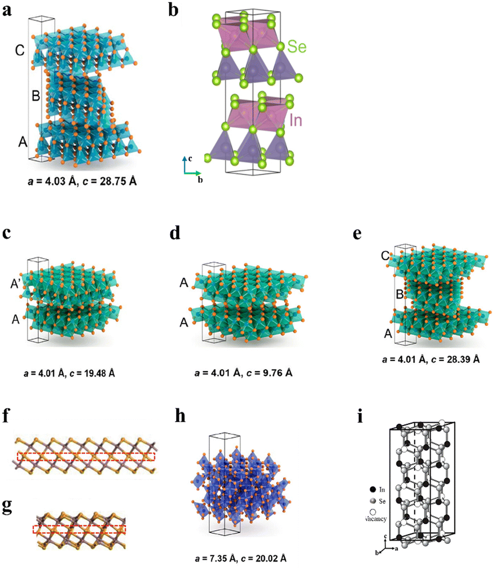 | ||
| Fig. 2 3D unit cell views and the crystal structure diagrams of common In2Se3 polytypes: (a) α(3R)-In2Se3, (b) α(2H)-In2Se3, (c) β(2H)-In2Se3, (d) β(1T)-In2Se3, (e) β(3R)-In2Se3, (f) β′-In2Se3, (g) β′′-In2Se3, and (h) and (i) γ-In2Se3. Reprinted with permission from ref. 30. Copyright 2021 American Chemical Society. Reprinted with permission from ref. 73. Copyright 2023 American Chemical Society. Reprinted with permission from ref. 76. Copyright 2023 The Japan Society of Applied Physics.30,73,76 | ||
The observed structural differences arise from variations in stacking sequences, bonding geometries of In/Se atoms, and the distribution of vacancies within the In2Se3 structure.31,33,77–79 These variations lead to distinct electrical and optical properties. For example, due to its non-centrosymmetric crystal structure, α-In2Se3 exhibits 2D ferroelectricity at room temperature. Similarly, β′-In2Se3 and γ-In2Se3 also exhibit ferroelectric properties, which are discussed further below.
2.2 Band structures of each phase of In2Se3
The band structure serves as a fundamental determinant in dictating the electronic and optical behaviors of materials.77,80 It provides a profound understanding of how electrons move, interact, and respond to external stimuli, thereby governing crucial properties like conductivity, absorption, and emission spectra.81,82 In2Se3 has various phases, mainly including α, β, and γ phases, exhibiting distinct structural characteristics. Importantly, these phase differences translate into significant variations in the band structure. In the context of applications, such as in photodetectors, the unique bandgap and energy band dispersion of each phase can directly influence the device's sensitivity and spectral response range, due to pronounced quantum confinement,83 as the thickness alters from 95 to 3.1 nm.84 Moreover, for bulk and multilayer α-In2Se3, the band gap is of a direct nature at a value of 1.453 eV.85 Single-crystal β-In2Se3 bulk is metastable, while 2D β-In2Se3 layers are stable at room temperature and ambient pressure.85 β-In2Se3, an n-type semiconductor, has a direct bandgap of 1.3 eV in bulk or few-layer form, but an indirect bandgap of 1.55 eV in monolayers.82,83 Although α-In2Se3 and β-In2Se3 have similar bandgaps, their band structures and intrinsic defect levels differ, leading to distinct electronic properties. In β-In2Se3, intrinsic defects act as shallow levels, enhancing conductivity, whereas in α-In2Se3, they likely act as deep levels, contributing little. Thus, α-In2Se3 behaves like a semiconductor,86 while β-In2Se3 exhibits metal-like characteristics. β′-In2Se3 is an n-type indirect semiconductor with strong two-dimensional characteristics, showing minimal variation perpendicular to the layers. Its maximum direct band gap is ∼1.77 eV, increasing to 2.5 eV in monolayer form.87 The Fermi surface in the conduction band exhibits strong in-plane dispersion around![[M with combining macron]](https://www.rsc.org/images/entities/char_004d_0304.gif) , suggesting high electron mobility. Additionally, β′-In2Se3 has significantly lower resistance than β-In2Se3. γ-In2Se3 functions as an n-type semiconductor, featuring a direct bandgap that varies with thickness, typically between 2.05 and 2.55 eV.26,88 Its electronic conductivity is extremely low, resembling that of an insulator.89
, suggesting high electron mobility. Additionally, β′-In2Se3 has significantly lower resistance than β-In2Se3. γ-In2Se3 functions as an n-type semiconductor, featuring a direct bandgap that varies with thickness, typically between 2.05 and 2.55 eV.26,88 Its electronic conductivity is extremely low, resembling that of an insulator.89
3. Preparation methodologies and characterization of In2Se3 polymorphism
3.1 Synthesis and preparation techniques for In2Se3
From an application standpoint, developing a reliable strategy for synthesizing two-dimensional In2Se3 nanosheets with precise thickness control and uniformity across large areas is crucial. Several synthesis methods have been proposed to produce In2Se3, each with varying levels of quality and scalability. These methods primarily include chemical vapor deposition (CVD), molecular beam epitaxy (MBE), and mechanical exfoliation. Among these, CVD stands out as the most commonly used technique for growing high-quality In2Se3 films. It offers precise control over the film thickness and phase, making it a preferred method for fabricating In2Se3 with the desired properties.90 Unlike mechanical exfoliation, which can introduce defects at the edges of transferred materials and make precise thickness control difficult, CVD can produce high-quality single-layer or few-layer In2Se3 materials under relatively mild conditions.57 CVD can offer the advantage of a larger growth area and more uniform material properties.30In a typical CVD process, In2Se3 samples are grown in a furnace with three independent temperature zones within a quartz tube. The polymorphs and crystal structures of the resulting In2Se3 primarily depend on factors such as growth temperature, heating position, and substrate choice.64,91 The selection of substrates is crucial in the CVD process.57 Selenium pellets, indium(III) oxide (In2O3) and hydrogen (H2) were used as reactants. Usually, selenium, In2O3 and the growing substrate were placed in the upstream, middle and downstream zones respectively. During the growth process, a mixture of argon (with a flow rate of 15–30 standard cubic centimeters per minute) and hydrogen (with a flow rate of 4 standard cubic centimeters per minute) was used as the carrier gas. A schematic illustration of the CVD growth is shown in Fig. 3a.92 For instance, when growing α-In2Se3 on an SiO2/Si substrate, selenium, In2O3, and the substrate are heated to 270 °C, 850 °C, and 750 °C, respectively, within 30 minutes, and held at these temperatures for 5 minutes. Fig. 3b exhibits an optical image of few-layer In2Se3 on mica, and the AFM images in Fig. 3c exhibit high spatial homogeneity and a film thickness of ∼7 nm. For synthesizing 2H β-In2Se3 on highly oriented pyrolytic graphite (HOPG), the heating temperatures for selenium, In2O3, and the substrate are set to 270 °C, 750 °C, and 640 °C, respectively. When growing γ-In2Se3 on an SiO2/Si substrate, the same temperatures and substrate are used as for α-In2Se3, except the substrate is positioned further downstream.93
 | ||
| Fig. 3 (a) Schematic illustration of the CVD growth set-up using In2O3 and Se powder. (b) Optical microscope images of In2Se3 on mica substrate after growth. (c) Atomic force microscope image of In2Se3. (d) Schematic diagram of the MBE system utilized for the synthesis of 2D In2Se3. (e) The mechanisms of molecular behaviors during epitaxial growth, and the optical microscope images and TEM image. (f) Schematic illustration of the different growth conditions required to selectively grow the different binary phases of InSe. (g) AFM topography of the as-grown InSe, the mixed InSe and In2Se3, and α-In2Se3. (h) Schematic illustration of the PLD growth. (i) AFM images for the In2Se3 thin films grown at (i) 1 mT, (ii) 10 mT and (iii) 100 mT deposition pressures by PLD. Reprinted with permission from ref. 92. Copyright 2022 Wiley-VCH GmbH.92 Reprinted with permission from ref. 94. Copyright 2018 American Chemical Society 2024 The Authors.94 Reprinted with permission from ref. 95. Copyright 2018 American Chemical Society.95 Reprinted with permission from ref. 96. Copyright 2022 Published by Elsevier B.V.96 | ||
In contrast, MBE, which involves the chemical reaction of precursor species in an ultra-high vacuum, allows for epitaxial growth of high-quality, ultrathin 2D In2Se3 layers with atomic-scale precision. Wu et al. achieved the growth of large-area, atomic layer flatness, and pure-phase β-In2Se3 using MBE and a detailed diagram of the MBE system is shown in Fig. 3d, which is for growing a series of 2-inch β-In2Se3 nano thin films. The growth temperature was carefully set at 480 °C, and the selenium to indium flux ratio (RSe/In) was systematically varied from 1 to 100. The mechanisms of molecular behaviors during epitaxial growth, and the optical microscope images and TEM image are shown in Fig. 3e. Fig. 3f shows a hypothetical model of samples with different Se/In flux ratios. A lower chemisorption energy is beneficial for horizontal growth, while a higher one results in smaller 2D flake sizes. To achieve large-scale two-dimensional van der Waals growth, it is necessary to control the chemisorption energy and maintain an appropriate physisorption potential energy. Increasing the proportion of selenides may help achieve this. The selected area electron diffraction (SAED) pattern shown in Fig. 3e was collected to investigate the crystallographic planes at the β-In2Se3 and sapphire interface. The regular diffraction points indicate that the β-In2Se3 film has a single crystal structure epitaxially grown on a C-plane sapphire substrate. Poh et al. successfully grew centimeter-sized monolayer α-In2Se3 films using the Frank–van der Merwe growth mode, employing the co-evaporation of In2Se3 and Se powders as the starting materials.95 Fig. 3f shows a schematic diagram of the MBE system used for synthesizing 2D In2Se3. This method resulted in highly crystalline, uniform, and continuous monolayers at a temperature of around 250 °C, which is significantly lower than that required for typical CVD processes. Fig. 3g analyzes the morphology of the films grown under different conditions using AFM. Compared to InSe, the nucleation density of α-In2Se3 is much lower and its grains are larger, better-faceted, and highly oriented. However, the AFM of the mixed-phase indium selenide shows a similar grain size to that of pure InSe. It is notable that there is buckling of grain boundaries in the mixed-phase indium selenide, which may be due to the lateral lattice mismatch of InSe and α-In2Se3. They also reported the non-layered growth of γ-In2Se3 on the SiO2/Si substrate using the same growth parameters, which further confirms the incompatibility between SiO2 and In2Se3.97 MBE, with its ability to produce high-purity, defect-free films, is particularly well-suited for research and high-performance applications, offering precise control over film quality and thickness at the atomic scale.
Mechanical exfoliation from the bulk crystal using adhesive tape is the most well-known method for producing high-quality atomically thin 2D flakes.98–101 The adhesive force between the tape and the top layers of In2Se3 is strong enough to overcome the weak van der Waals (vdW) interaction between two adjacent layers in a bulk crystal, thus achieving layer-by-layer separation. In contrast, the ionic-covalent (IP) bonds within each layer remain intact and the crystallinity is preserved, which is highly attractive for fundamental research on intrinsic properties and for achieving excellent device performance. However, the limited lateral dimensions, uncontrolled thickness uniformity, and extremely low yield of the exfoliated flakes hinder their applications in large-scale device development and array integrations.102
Pulsed laser deposition (PLD), schematically illustrated in Fig. 3h, is a versatile thin-film synthesis technique that utilizes high-energy pulsed laser ablation of a target material to deposit stoichiometric films on a substrate. Chanchal et al. employed PLD to synthesize phase-defined In2Se3 thin films by precisely controlling the deposition pressure (1–100 mTorr) in a nitrogen ambient.96 The AFM images of the as-grown In2Se3 films are shown in Fig. 3i. At 1 mTorr (Fig. 3i(i)), the Se-deficient environment facilitated the growth of layered 3R α-In2Se3, while higher pressures (10 mTorr) induced the formation of β-In2Se3 with excess Se due to increased Se flux which is shown in Fig. 3i(ii). At 100 mTorr (Fig. 3i(iii)), non-layered γ-In2Se3 dominated under Se-rich conditions. Jeengar et al. demonstrates the fabrication of a high-performance NO2 gas sensor using bilayer α-In2Se3 thin films grown via PLD.103 The results highlight PLD's capability to produce ultrathin, high-quality α-In2Se3 films for low-power gas-sensing applications. Zheng et al. indicates that photodetectors made using centimeter-scale, high-quality In2Se3 films grown on various substrates via a PLD technique exhibit outstanding photoresponses.104 In conclusion, compared to CVD, PLD offers precise stoichiometry and uniformity. MBE provides high crystallinity but requires ultra-high vacuum and slow growth, while PLD operates at lower Torr with faster rates. Unlike mechanical exfoliation, PLD enables large-area films with tunable thickness, essential for optoelectronic devices.
Moreover, flash-within-flash (FWF) Joule heating is a novel synthesis technique developed in recent years. The FWF method enables gram-scale synthesis of α-In2Se3 crystals by overcoming the conductivity limitations of precursors through indirect Joule heating. Shin et al. successfully achieved the production of high-purity, single-phase α-In2Se3 by FWF for neuromorphic computing applications.105
3.2 Characterization of In2Se3 polymorphism
Given the complex polymorphism of In2Se3, it is essential to distinguish between its various crystal structures using nondestructive characterization and imaging techniques. Key methods typically employed for this purpose include transmission electron microscopy (TEM), Raman spectroscopy, and X-ray diffraction (XRD). These techniques provide valuable insights into the material's structural properties without compromising its integrity.2D In2Se3 can be precisely characterized in terms of its nanoscale crystal structure, lattice defects, and crystal orientations using TEM, a high-resolution technique that transmits an electron beam through the sample. High-angle annular dark-field (HAADF) imaging, a mode of TEM, enhances contrast based on electron scattering angles, providing valuable insights into elemental distribution. Both TEM and HAADF are essential for characterizing 2D In2Se3. The α and β polymorphs exhibit distinct intralayer quintuple atomic arrangements, as shown in Fig. 2, making them identifiable through cross-sectional TEM imaging. To distinguish α- and β-In2Se3 more clearly, it is necessary to analyze the layer stacking sequences, as illustrated by TEM. As shown in Fig. 4a, the α(3R)-In2Se3 features a unit cell with no mirror symmetry among its layers, with each layer undergoing a lateral translation relative to its predecessor. For β(2H)-In2Se3, shown in Fig. 4d, the unit cell consists of two quintuple layers, with alternating mirrored layers that form a zigzag pattern. In contrast, γ-In2Se3, as delineated in Fig. 4g, displays a van der Waals ordered superstructure framework (VOSF) configuration, with a periodic length of 20.02 Å corresponding to the d spacing of ss planes in the γ-In2Se3 crystal lattice,106 rather than following a conventional layered structure.77
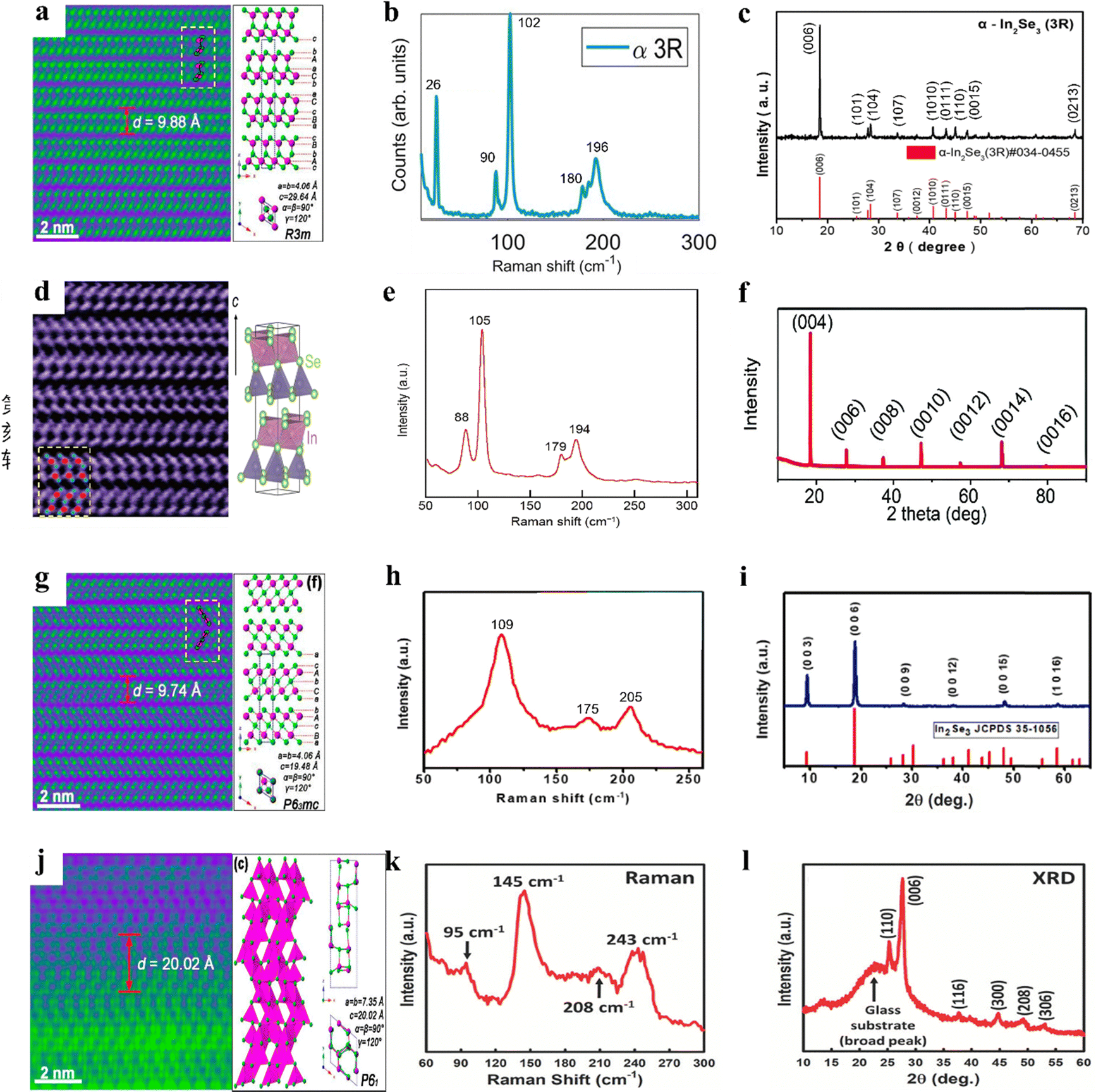 | ||
| Fig. 4 Characterization of In2Se3. (a) TEM, (b) Raman and (c) XRD of α(3R)-In2Se3. (d) TEM, (e) Raman and (f) XRD of α(2H)-In2Se3. (g) TEM, (h) Raman and (i) XRD of β(2H)-In2Se3. (j) TEM, (k) Raman and (l) XRD of γ-In2Se3. Reprinted with permission from ref. 107. Copyright 2024 American Chemical Society. Reprinted with permission from ref. 108. Copyright 2018 WLEY-VCH Verlag GmbH & Co. KGaA, Weinheim. Reprinted with permission from ref. 5. Copyright 2022 Science China Press and Springer-Verlag GmbH Germany, part of Springer Nature. Reprinted with permission from ref. 109. Copyright 2021 Elsevier Ltd. Reprinted with permission from ref. 75. Copyright 2023 Wiley-VCH GmbH. Reprinted with permission from ref. 93. Copyright 2019 American Chemical Society.5,75,93,107–109 | ||
In addition, Raman spectroscopy is a primary characterization technique for phase identification of In2Se3, leveraging its sensitivity to high-frequency modes that inherently reflect the phase-dependent characteristics. Fig. 4b showcases the micro-Raman spectrum of α(3R)-In2Se3, unveiling prominent Raman peaks at 90, 102, 180, and 196 cm−1, corresponding to the E2, A11, E4 and A21 vibration modes, respectively.85,106,110–112 α(2H)-In2Se3 was confirmed by the Raman spectrum,113 which reveals vibration peaks at 88, 105, 179, and 194 cm−1 and is depicted in Fig. 4e.32,113 The Raman spectrum can be utilized to discern the difference between these two structures. Specifically, one of the Raman peak values of α-In2Se3, which is 90 cm−1 (E2), is conspicuously observable in the hexagonal structure (2H), whereas it is less distinct in the rhombohedral structure (3R), likely making the intensity ratio between the E2 and A11 modes a distinguishing fingerprint for 2H and 3R α-In2Se3. Conversely, β(2H)-In2Se3 presents a distinct triad of characteristic peaks at 109, 175 and 205 cm−1 depicted in Fig. 4h, which are different from those of α(3R)-In2Se3.93,114 β′-In2Se3 is typically considered a derivative of the β phase,74 so they have few differences in their Raman spectra. What is worth mentioning is that distinguishing among 1T, 2H and 3R β-In2Se3 crystals in the Raman spectra at room temperature is challenging. In contrast, γ-In2Se3, characterized by a non-layered crystal structure, lacks additional polytypes, rendering its identification relatively straightforward among the common polymorphs. It exhibits a singular principal Raman peak at 150 cm−1 as shown in Fig. 4k.75
Furthermore, XRD is commonly used to characterize the different phases of In2Se3, as it relies on the lattice parameters of a crystalline material to produce diffraction patterns that are unique to each phase. However, as shown in Fig. 4c and f, the differences in lattice parameters between α- and β-In2Se3 are minimal, making XRD less effective for distinguishing between these phases. In contrast, TEM offers superior phase identification.106,109 XRD can, however, reliably identify γ-In2Se3, with characteristic peaks observed at 2θ values of 25° and 27.5° for the (110) and (006) facets, respectively, as shown in Fig. 4i.73
4. Comparative properties of In2Se3 polymorphism
4.1 Electrical properties of In2Se3 polymorphism
The three prevalent phases of In2Se3 exhibit distinct electrical properties and optoelectronic characteristics due to structural discrepancies previously delineated. Zheng et al. investigated the electrical properties of 2D In2Se3 devices by applying continuous, milder bias/current using the in situ TEM technique.115 The schematic of the devices is shown in Fig. 5a. They measured the I–V characteristics across different phases of In2Se3 using point-like contacts, as illustrated in Fig. 5b. The results indicate superior conductivity in α-In2Se3 and β′-In2Se3 compared to γ-In2Se3. Subsequent cyclic biasing across the different phases revealed distinct behaviors. Notably, resistive hysteresis was observed in α-In2Se3 after multiple I–V cycles during the electroforming process, as shown in Fig. 5c and d, and further detailed in Fig. 5g. In contrast, β′-In2Se3 (Fig. 5e) and γ-In2Se3 (Fig. 5f) did not exhibit the resistive memory effect observed in α-In2Se3. This absence of resistive switching in β′-In2Se3 and γ-In2Se3 is likely due to their weaker ferroelectric polarization compared to α-In2Se3, despite the confirmed ferroelectric properties of all three materials. | ||
| Fig. 5 (a) A schematic of the In2Se3 FET. (b) I–V curves of the three common phases of In2Se3. (c) and (d) The electroforming process of α-In2Se3. (e) I–V cycles of β′-In2Se3. (f) I–V cycles of γ-In2Se3. Reprinted with permission from ref. 115. Copyright 2022 The Authors.115 | ||
4.2 Ferroelectric polarization
Ferroelectric polarization is a critical property of In2Se3 that significantly influences its electrical and optoelectronic behavior. Cui et al. investigated this phenomenon in α- and β-In2Se3 flakes using piezoresponse force microscopy (PFM).116 The PFM amplitude signifies the local piezoelectric contrast's strength, while the phase reveals the ferroelectric polarization's direction. As shown in Fig. 6a, the AFM image indicates α-In2Se3 flakes range from 2–6 nm in thickness. Upon scrutinizing the out-of-plane (OOP) images, as depicted in Fig. 6b (amplitude) and Fig. 6c (phase), alongside the in-plane (IP) counterparts portrayed in Fig. 6d (amplitude) and Fig. 6e (phase), the discernment of singular ferroelectric domains within each terrace for α-In2Se3 emerged conspicuously. Such observations suggest that α-In2Se3 can spontaneously achieve a singular domain state devoid of external electric field perturbations, with the notable finding that its IP polarization magnitude surpassed its OOP counterpart. In non-volatile memory applications like ferroelectric field-effect transistors (FeFETs), the polarization states of ferroelectric properties can represent “0” and “1” in binary data. For example, upward polarization can denote “1”, and downward polarization represents “0”. When applying appropriate voltage pulses, the polarization direction of the In2Se3 material can be changed to achieve data writing.106,117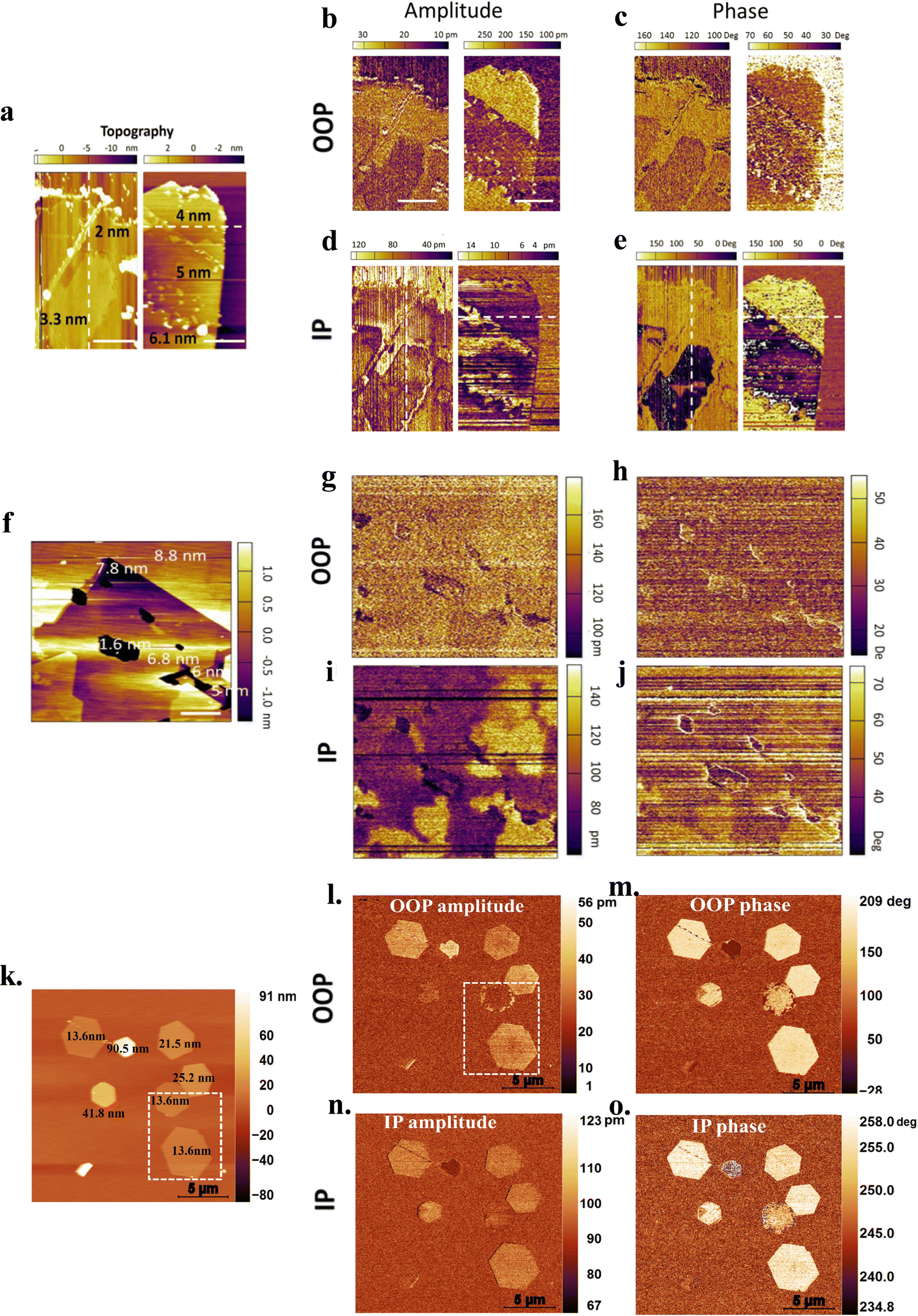 | ||
| Fig. 6 AFM and PFM images of thin flakes for different In2Se3 phases: (a) AFM image of α-In2Se3 flakes with the corresponding OOP PFM images showing (b) amplitude and (c) phase, as well as IP PFM images depicting (d) amplitude and (e) phase. Similarly, for β-In2Se3: (f) AFM image, (g) OOP PFM amplitude, (h) OOP PFM phase, (i) IP PFM amplitude, and (j) IP PFM phase. For γ-In2Se3: (k) AFM image, (l) OOP PFM amplitude, (m) OOP PFM phase, (n) IP PFM amplitude, and (o) IP PFM phase.116,118 Reprinted with permission from ref. 116. Copyright 2018 American Chemical Society. Reprinted with permission from ref. 118. Copyright 2021 Elsevier B.V. | ||
Moving forward, Cui et al. examined the ferroelectric response of α-In2Se3 when subjected to electric fields, as well as the duration of its ferroelectric state.116 They discussed the stability of this state and its switchability under an external electric field, which is essential for memory applications.119 As shown in Fig. 7, it is evident that after applying −6 V and +6 V stripes, the PFM image of a 6 nm α-In2Se3 distinctly reveals high and low current states, corresponding to opposing polarization states.31,120 What is more, the voltage-induced domain states in 6 nm flakes persist for up to 3 hours. Fig. 6g–i provide further insight into how the polarization within α-In2Se3 is manipulated by an external electric field. This modulation significantly impacts the current and conductance of the channel, showcasing nonvolatile memory effects. In Fig. 6h, α-In2Se3 resets at 1.75 V during the initial positive I–V cycle and sustains the reset state upon subsequent cycles, indicating its potential for nonvolatile memory. This can be recovered under negative bias (Fig. 6i).120
 | ||
| Fig. 7 The stability of the as-written domains on 6 nm thick α-In2Se3 (scale bar: 1 μm).116 Reprinted with permission from ref. 116. Copyright 2018 American Chemical Society. | ||
However, Bai et al. recently suggested that the in-plane ferroelectricity of α-In2Se3 may have been overestimated.121 Through experimental characterization and symmetry analysis, they refute previous claims of in-plane ferroelectricity in single-domain α–α-In2Se3. Additionally, deep-learning-assisted molecular dynamics simulations reveal that the vertical polarization switching mechanisms in monolayer α-In2Se3 differ fundamentally from those in bulk ferroelectrics. Angle-resolved PFM shows the in-plane response stems from out-of-plane signal crosstalk, not intrinsic piezoelectric effects. Their findings clarify misunderstandings about α-In2Se3's ferroelectric properties and provide quantitative insights into domain wall behavior in 2D ferroelectric α-In2Se3.
γ-In2Se3 has a non-centrosymmetric structure.41,74,122,123 Rashid et al. determined the ferroelectric properties of γ-In2Se3 in both IP and OOP directions by PFM, which is relatively shown in Fig. 6l–o.118 Conversely, the absence of ferroelectric behavior was ascertained for β-In2Se3. This assertion was corroborated by the absence of discernible phase contrast distinctions in either IP (Fig. 6i and j) or OOP (Fig. 6g and h) orientations, attributable to the intrinsic lack of a ferroelectric phase in β-In2Se3. This conclusion harmonizes with the known structural attributes of β-In2Se3, characterized by centrosymmetric arrangements that preclude ferroelectricity. Notably, β′-In2Se3, as a typically derivative of β-In2Se3, has additional structural modulation in the form of 1D nano stripes. By virtue of second-harmonic generation, four-dimensional STEM, and in-plane piezoresponse force microscopy, the long-range inversion-breaking symmetry, uncompensated local polarization, and net polarization domains are unambiguously verified, revealing β′-In2Se3 as an in-plane ferrielectric layered material.41,74,122,123
4.3 Optoelectronic characteristics
2D materials have garnered significant attention in optoelectronics due to their unique light–matter interaction and high carrier mobility.124 In2Se3 stands out as a promising 2D semiconductor with effective light absorption and carrier generation properties. The different phases of In2Se3, α, β, and γ, exhibit distinct bandgaps, ranging from 1.39–1.45 eV for α and β-In2Se3, and 2–2.52 eV for γ-In2Se3, making them suitable for broadband photodetection across ultraviolet (UV) to near-infrared (NIR) wavelengths.125 Notably, phase transitions in In2Se3 play a significant role in modulating its optical characteristics, thereby influencing its optoelectronic performance. This section explores the optoelectronic properties of these phases, providing crucial insights into their potential applications in various optoelectronic devices.As for optoelectronic applications,125 α-In2Se3 can be seamlessly integrated with 3D materials. For instance, Jia et al. introduced a device incorporating a hybrid-dimension α-In2Se3/Si vertical heterojunction, illustrated schematically in Fig. 8a.126 This innovative setup resulted in a photodetector, showcased in Fig. 8b, exhibiting exceptional sensitivity to incident light. Fig. 8b illustrates that within the 405–980 nm spectral range, the α-In2Se3/Si heterojunction demonstrates remarkable photoresponse, surpassing an Ion/Ioff ratio of 105 and a fast response to rapidly switching optical signals about the μs level. Additionally, it is suggested that the ferroelectric modulation of α-In2Se3 also contributes synergistically to its photoelectric properties. Fig. 8c illustrates the wavelength-dependent responsivity and enhancement photoresponsivity ratio (Rup/Rdown), demonstrating the discrepancy in light response to various wavelengths between the Pup and Pdown states. Clearly, the photoresponsivity of the photodetector varies significantly across different ferroelectric polarization states.
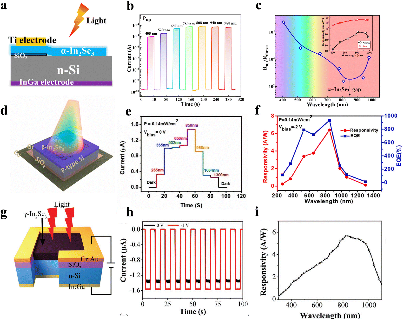 | ||
| Fig. 8 α-In2Se3/n-Si ferroelectric heterojunction. (a) A schematic diagram. (b) The time response under different wavelength illumination. (c) The responsivity ratio as a function of incident light wavelength. β-In2Se3/n-Si ferroelectric heterojunction: (d) A schematic. (e) The time response under different wavelength illumination. (f) The wavelength dependent responsivity and EQE curves. γ-In2Se3/n-Si ferroelectric heterojunction: (g) A schematic. (h) The time response, measured at bias voltages of 0 and −1 V, under 808 nm light illumination. (i) The wavelength dependent responsivity. Reprinted with permission from ref. 126. Copyright 2023, The Authors, published by American Chemical Society. Reprinted with permission from ref. 127. Copyright 2017 American Chemical Society. Reprinted with permission from ref. 128. Copyright 2017 Wiley-VCH Verlag GmbH & Co. KGaA, Weinheim.126–128 | ||
β-In2Se3 also demonstrates considerable potential for optoelectronic applications. For instance, Guo et al. successfully fabricated a high-speed, broad-spectrum β-In2Se3/Si p–n photodetector utilizing the pulsed laser deposition (PLD) technique, as shown in Fig. 8d.109,127 The β-In2Se3/Si photodetector demonstrated outstanding device performance, featuring a wide response broadband spectrum spanning from 265 to 1300 nm as depicted in Fig. 8e, a high responsivity up to 6.4 A W−1 shown in Fig. 8f (by the red line), and a high response speed approaching 2.2 μs at zero bias. Notably, these characteristics surpass those of many previous III–VI/Si based photodetectors and certain 2D TMDCs/Si heterojunctions.124
As for γ-In2Se3, Chen et al. fabricated a high-quality γ-In2Se3/Si heterojunction photodiode,128 as illustrated schematically in Fig. 8g. The photodiode demonstrates exceptional responsivity and detectivity across a wide range of wavelengths, making it a compelling candidate for highly efficient photodetectors. Fig. 8i shows the device's performance under dark conditions and various light intensities (380, 680, and 880 nm) from Xenon lamps. Notably, the photoresponsivity peaks at 5.67 A W−1 at 820 nm, far exceeding the typical 0.8 A W−1 of commercial Si-based photodetectors. Fig. 8h presents time-resolved photoresponse curves under 808 nm laser illumination at 0 and −1 V bias, demonstrating the heterojunction's rectifying nature and confirming its functionality as a photodiode.
The three types of In2Se3-based photodetectors exhibit exceptional optoelectronic characteristics, highlighting their potential in a wide range of photonic applications. Each detector demonstrates high photoresponsivity, indicating their sensitivity to light, especially in the UV to near-infrared spectrum. Overall, these In2Se3-based photodetectors, in their different phases (α, β, and potentially γ), offer diverse and complementary properties, making them attractive candidates for a wide range of photonic applications where sensitivity, speed, and broadband response are critical.
Table 1 consolidates a comprehensive summary of the properties and applications of the various phases of In2Se3. It succinctly outlines the distinctive characteristics and potential utilizations of each common phase, namely α, β, β′, and γ, highlighting their differences in terms of structural, ferroelectric, and optical properties. Through a comparative analysis of these properties, a more profound comprehension can be attained regarding the potential utilization of the different phases of In2Se3 for specific technological applications, including but not limited to optoelectronics, photodetectors, and data storage systems.
| Phase | Morphologies | Ferroelectric | Optoelectronic | Application | Ref. |
|---|---|---|---|---|---|
| α | Monolayer | IP and OOP | Wavelength: 405–1550 nm | Photodetector, memory, synaptic transistor | 39, 93 and 129 |
| 2H (bulk) | Layer dependence | Responsivity: 347 A W−1 | |||
| 3R (bulk) | IP and OOP | For 520 nm, 0.49 mW cm−2 | |||
| β | Monolayer | None | Wavelength: 265–1300 nm | Photodetector | 62, 93 and 109 |
| 1T | None | Responsivity: 6.4 A W−1 | |||
| 2H | None | For 850 nm, 0.14 mW cm−2 | |||
| β′ | Monolayer | IP | None | Memory | 41, 130 and 131 |
| γ | P61 | IP and OOP | Wavelength: 300–1100 nm | Photodetector, memory | 75, 118 and 128 |
| Responsivity: 5.67 A W−1 | |||||
| For 820 nm | |||||
The intense optical absorption within the visible to near-infrared wavelength range, the phase-dependent direct bandgap, and the moderate mobility render In2Se3 a potential candidate for photodetection. Additionally, by taking advantage of its ferroelectric properties, the amplitude of the photocurrent can be modulated. Li et al. mentioned that a systematic exploration on the atomic structures and optical properties of polymorphic In2Se3 through density functional theory (DFT) calculations,43 revealing critical insights into its phase-dependent electronic behavior and stability. For the α state, the calculated optical bandgap was determined to be 1.44 eV, while its fundamental indirect bandgap was 1.34 eV.132 The extinction coefficient (k) of it decreased sharply beyond 800 nm. Regarding the β state, the optical bandgap was 1.27 eV, and its fundamental indirect bandgap was significantly smaller, being 0.46 eV, and the value of k gradually decreased from 800 nm to 1400 nm and was less than 10−5 at 1550 nm.132 To ensure transparency at telecommunication wavelengths, both optical bandgaps exceeded 0.8 eV. These differences in bandgaps serve as the foundation for the phase transition applications of In2Se3, enabling a significant refractive index contrast in optoelectronic devices.
4.4 Layer-dependent properties of In2Se3
The electronic and optical properties of 2D In2Se3 vary significantly with the number of layers, making it highly versatile for optoelectronic applications.97For α-In2Se3, the thickness-dependent bandgap is particularly advantageous for applications like photodetectors, as it allows for the selection of the desired photonic energy window by simply adjusting the material thickness. Atomically thin α-In2Se3 crystals exhibit a substantial quantum confinement effect, which influences their optical properties. Quereda et al. demonstrated that as the thickness of α-In2Se3 varies from 3.1 nm (approximately 3 layers) to 95 nm (more than 90 layers), the optical transmittance decreases monotonically at a fixed illumination wavelength.84,133 In fact, the band gap variation observed in atomically thin In2Se3 due to the effect of quantum confinement is among the largest reported to date in 2D semiconductor materials, and is comparable to that of atomically thin black phosphorus (as shown in Fig. 9a). For γ-In2Se3, the direct bandgap ranges from approximately 2.05 eV to 2.55 eV depending on the layer thickness.134
 | ||
| Fig. 9 (a) Comparison of the band gap values for different van der Waals semiconductor crystals. The horizontal bars spanning a range of energies indicate that the band gap can be tuned over that range by changing the number of layers. (b) Thickness-dependent transmittance spectra of the γ-In2Se3 layered crystals. The lower inset shows an energy window of about 0.4 eV for the band gap difference between 6 μm and 125 μm thick samples. (c) The ratios of >30 deg phase area in the different layers. Reprinted with permission from ref. 84. Copyright 2016 Wiley-VCH GmbH.84 Reprinted with permission from ref. 134. Copyright 2013 Royal Society of Chemistry.134 Reprinted with permission from ref. 4. Copyright 2014 Royal Society of Chemistry.4 | ||
In terms of optical absorption, the absorption coefficient of In2Se3 is also thickness-dependent. According to the Tauc model, the optical band gap strongly depends on the flake thickness, increasing from 1.45 eV for thicker flakes to 2.8 eV for the thinnest studied.135 The inset in Fig. 9b indicates that the optical gap energy window for two samples with different thicknesses (6 mm and 125 mm) is approximately 0.4 eV, which implies that γ-In2Se3 layers can be used to fabricate an optical-logic switch for a common 532 nm laser for communication purposes.
In addition to optical properties, ferroelectric polarization also exhibits significant dependence on the number of layers. Through analysing the phase area from PFM, the ratios of >30 deg phase area in the different layers were obtained and displayed in Fig. 9c. In 2H-stacked α-In2Se3 nanoflakes, the magnitude and reversal of polarization show this oscillation. For odd layers (OL), the IP polarization is larger than for even layers (EL), and when IP is reversed, OL's OOP polarization exceeds that of the ELs. Samples with aligned OOP polarization also show IP polarization's odd–even dependence. This property is due to the IP anti-parallel arrangement of adjacent layers in 2H stacking and the strong coupling between OOP and IP.4 Using odd and even layers as different storage units can store more information by controlling polarization states. In addition, utilizing the negative differential resistance (NDR) characteristic is another important application advantage brought about by the odd–even layer-dependent ferroelectric polarization phenomenon, which can realize multifunctional logic circuits.136,137
The electrical properties of In2Se3 including ferroelectric, thermoelectric, and optoelectronic characteristics, are all influenced by the number of layers. For instance, multilayer β-In2Se3 can exhibit enhanced light absorption, making it more suitable for high-performance photodetectors. The ability to tune these properties by adjusting the layer number offers flexible solutions for designing next-generation optoelectronic devices, making In2Se3 a promising material for a variety of advanced electronic applications.
5. Phase transition modulation methodologies
The potential for fabricating controllable phase-change devices is appealing, given the rich array of physical and material characteristics exhibited by the various common phases of materials. However, despite these inherent attributes, the effective control of reversible phase transitions between them still remains a significant challenge.138 Therefore, it becomes imperative to comprehend the existing reversible phase transition methodologies applicable to In2Se3, with a view to refining and innovating upon them. This imperative is underscored by its pivotal role in advancing the development of non-volatile integrated photonic devices. To enhance the controllability and quality of phase transitions in In2Se3, a comprehensive understanding of the underlying phase switching techniques and mechanisms is indispensable.5.1 Temperature-dependent modulation of phase transitions
Temperature can serve as an effective tool for modulating the phase transitions of In2Se3. Many studies have observed distinct phase transitions in In2Se3 as it undergoes thermal treatment.25,42,64,77,85,139–145 For example, Hsu et al. investigated the phase transition behavior of In2Se3 by annealing as-deposited thin films (approximately 35 nm in thickness) at various temperatures.64 Their findings, shown in Fig. 10e, revealed four distinct stages of phase transition: amorphous, γ-phase, β-phase, and α-phase. Specifically, amorphous In2Se3 transformed into γ-In2Se3 at around 400 °C, followed by a transition to the β-phase at 700 °C. Interestingly, they also observed that the transition from the β-phase to the α-phase occurred at room temperature once the sample was removed from the furnace, as depicted in Fig. 10f. The phase of as-deposited In2Se3 annealed at different temperatures can be classified into amorphous/α/β/γ-In2Se3, each characterized by distinct Raman peaks, as shown in Fig. 10a–d.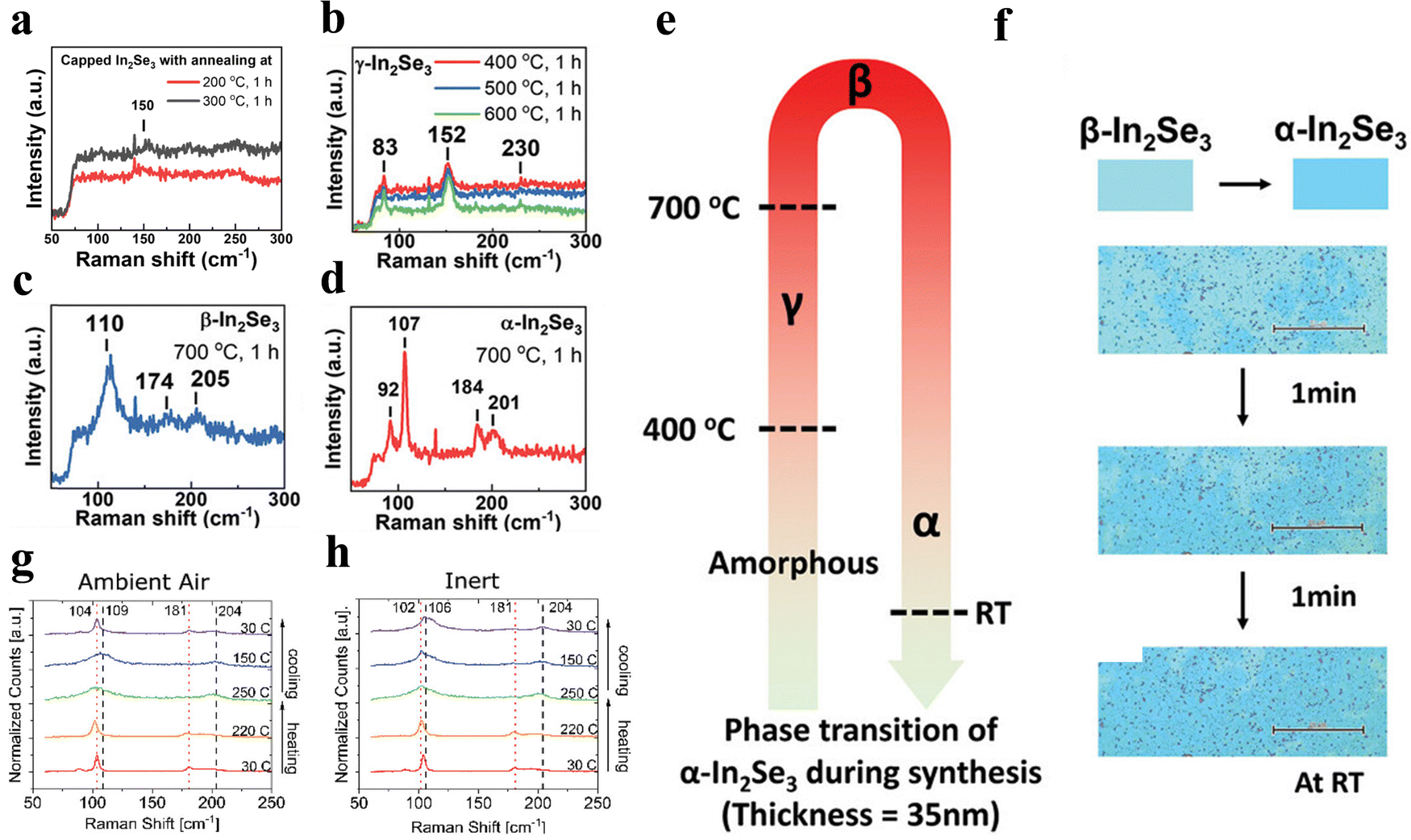 | ||
| Fig. 10 Raman spectra of In2Se3 annealed at various temperatures and at room temperature: (a) amorphous structure, (b) γ-In2Se3, (c) β-In2Se3, and (d) α-In2Se3. (e) Schematic phase transition of In2Se3 with a thickness of 35 nm. (f) Phase transition of In2Se3 after annealing at 700 °C for 1 h which was observed by an optical microscope at room temperature. Raman spectra of In2Se3 at various temperatures and various environments (g) measured in the atmosphere, and (h) in 99% purity argon. Reprinted with permission from ref. 64. Copyright 2024 The Authors, published by Wiley-VCH GmbH. Reprinted with permission from ref. 145. Copyright 2023 The Authors, published by Wiley-VCH GmbH.64,145 | ||
This temperature-induced phase modulation highlights the critical role of thermal treatment in controlling the structural properties of In2Se3, which is essential for tailoring its optoelectronic and electronic behaviors across various applications. Ignaci et al. investigated the α–β phase transformation in layered In2Se3, induced under varying environmental conditions, temperatures, and encapsulation methods.145 As shown in Fig. 10g and h, the α–β transformation was triggered by thermal excitations between 200 and 350 °C, irrespective of whether the samples were exposed to ambient air or an inert atmosphere. This transformation was identified by the A1(LO) phonon mode at 204 cm−1.63,93,110 Notably, during the cooling process, significant differences were observed: β-In2Se3 reverted to the α-phase in ambient air, while exhibiting stability in an inert environment. This suggests that the transition from β to α is facilitated by oxidative conditions. To mitigate this phase transition, the research team applied an encapsulating layer, such as graphene or hexagonal boron nitride (hBN).85 Their findings demonstrated that these encapsulation layers effectively prevented the transition from β to α phase.
5.2 Electrical stimuli modulation of phase transitions
While temperature-dependent modulation offers a primary means of inducing phase transitions in In2Se3, there are still limitations of using temperature alone for phase control in 2D In2Se3. For instance, elevating the temperature from room temperature to either 220 °C122 or 290 °C85 can induce a transition of 2D α-In2Se3 to β′-In2Se3. Nonetheless, once the temperature returns to room temperature, β′-In2Se3 does not revert to α-In2Se3.Recent studies have shown that electrical stimuli can also play a significant role in modulating its phase behavior. Zheng et al. explored alternative methods for phase modulation, suggesting that electrical stimuli could offer a more versatile and dynamic approach for controlling the phase transitions of 2D In2Se3.115 In particular, they discovered that an applied electric field can trigger a reversible phase shift between the β′ and non-layered γ phases of In2Se3, which shows promise for memristor applications. Through comprehensive in situ TEM analysis, Zheng et al. demonstrated that both electrical and mechanical stimuli could effectively manipulate the phases of 2D In2Se3, as shown in Fig. 11a and b. The influence of electrical stimuli on the material is attributed to both the electric field and the thermal effect. Fig. 11a presents the in situ electrical TEM setup used in their study. The experimental procedure reveals that with a low current, about 5 × 10⁻⁵ A, a phase transition from α-In2Se3 and β′-In2Se3 occurs. Increasing the current to ∼8 × 10⁻⁵ A results in a direct transformation from α-In2Se3 to γ-In2Se3.146 These results highlight how electrical current-induced heating can trigger phase transitions in 2D α-In2Se3, which offer valuable new insights into the phase manipulation of 2D materials. Wu et al. ulteriorly investigated the ferroelectric polarization switching mechanisms and phase transition behaviors of two-dimensional ferroelectric material α-In2Se3 under different stacking orders (2H and 3R) through in situ electrical STEM experiments and density functional theory (DFT) calculations.147
 | ||
| Fig. 11 (a) Electrical TEM and experimental procedure diagrams. (b) Strain-induced reversible phase transition. (c) High-pressure Raman spectra of α-In2Se3. (d) Atomic scheme of the phase transitions of In2Se3.115,148 Reprinted with permission from ref. 115. Copyright 2022 The Authors. Reprinted with permission from ref. 148. Copyright 2014 AIP Publishing. | ||
5.3 Strain-induced reversible phase transition modulation
Strain-induced reversible phase transition can also effectively modulate the phase transition in In2Se3.112,149,150 A schematic graph of the strain-induced reversible phase transition is shown in Fig. 11b. Zheng et al. used in situ TEM techniques to load or unload the mechanical strain on the In2Se3 samples.115 During the compression process, the β′-In2Se3 remains unchanged. When the tip is pulled back in the reverse direction, the transition from β′-In2Se3 to α-In2Se3 occurs due to strain relaxation. The reason why strain can cause the phase transition is that upon the TEM manipulation, when the tip moves away from the β′-In2Se3, the delamination between β′-In2Se3 and the substrate occurs with strain relaxation in β′-In2Se3. In this way, the tensile strain originally restored in β′-In2Se3 applied by the substrate is released, which results in the phase transition from β′-In2Se3 to α-In2Se3.47Similar to the strain-induced method, the application of pressure serves as a potent controlling factor for driving transformations.48,151–154 Ke et al. reported an anomalous phase transition in compressed In2Se3.148 Fig. 11c displays the high-pressure Raman spectra of In2Se3, revealing a clear transformation from rhombohedral to a new R![[3 with combining macron]](https://www.rsc.org/images/entities/char_0033_0304.gif) m structure at 0.8 GPa. This is evidenced by the emergence of new peaks at approximately 205 cm−1, which are attributed to β-In2Se3. The article states that this transition occurs due to a pressure-induced interlayer slide. The phase transition of In2Se3 can be achieved through various pathways, and the schematic diagram (Fig. 11d) encapsulates most of the current methods.
m structure at 0.8 GPa. This is evidenced by the emergence of new peaks at approximately 205 cm−1, which are attributed to β-In2Se3. The article states that this transition occurs due to a pressure-induced interlayer slide. The phase transition of In2Se3 can be achieved through various pathways, and the schematic diagram (Fig. 11d) encapsulates most of the current methods.
In addition, theoretical research to explain the crystal conversion principle of In2Se3 is also an important aspect. Modi et al. synthesized β′′-In2Se3 nanowires through experiments.155 Under a direct current bias, the electrical and microscopic structures of the nanowires changed. The varied I–V curve is illustrated in Fig. 12(f), in which amorphization occurs at 20 V and is preceded by a rapid decrease in current with time. What is more, the TEM characterization revealed the crystal-amorphous transformation and related structural changes, which are shown in Fig. 12(a) and (b). The contrast from the crystal-amorphous interface can be seen at the left side of the nanowire, where a part of the interface is shown in the TEM image in Fig. 12(c). Electron diffraction and HR-TEM images are shown in Fig. 12(d) for the paraelectric crystalline phase and in Fig. 12(e) for the amorphous regions of the nanowire device. The amorphization was affected by multiple factors rather than just heating, also involving the interaction of multiple factors such as the electric field and carrier force. The in situ TEM analysis observed the correlation between strain and current fluctuations and the dynamic process of amorphization.
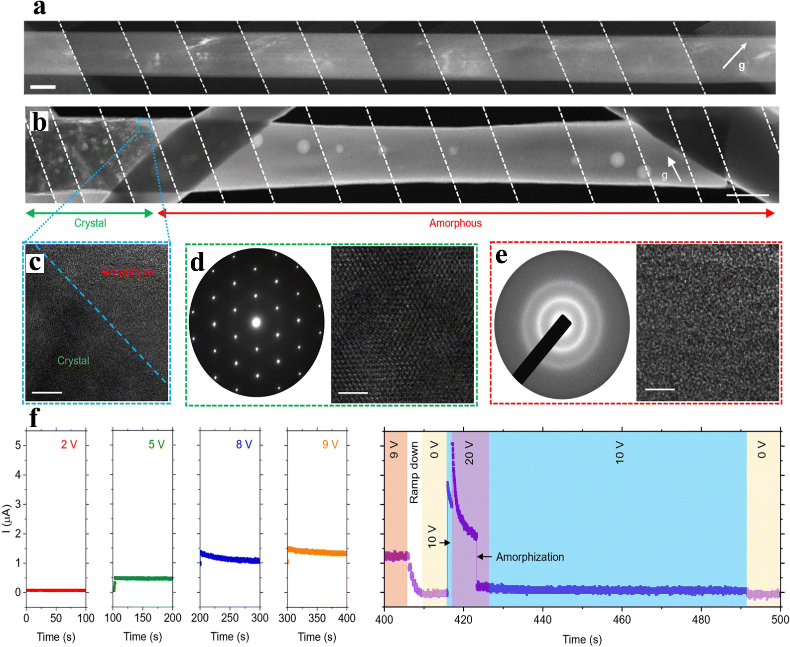 | ||
| Fig. 12 (a) The TEM image of a pristine nanowire device before applying any electrical stimuli. (b) The TEM image of the nanowire after amorphization. (c) The TEM image of part of the crystal-amorphous interface. (d) Electron diffraction from the paraelectric crystalline phase. (e) HR-TEM image of the amorphous regions of the nanowire device. (f) Evolution of current in the nanowire device with time when the device is held at different fixed dc voltages.155 Reprinted with permission from ref. 155. Copyright 2024 The Author, under exclusive license to Springer Nature Limited. | ||
6. Phase change applications of polycrystalline In2Se3
6.1 Hetero-phase junction
As mentioned above, 2D In2Se3 is attractive for its polymorphism. Also, hetero-phase junctions, also referred to as homoepitaxial heterojunctions, are composed of the same chemical elements or compounds. However, they exhibit significantly different physical and chemical properties due to variations in their internal atomic arrangements, spatial structures, or crystal forms.156 Hetero-phase junctions play a critical role in both material science and device applications, offering avenues for innovative materials and device performance enhancements.By forming hetero-phase junctions, novel properties emerge that are absent in the single phase.130,157–160 In2Se3, featuring an out-of-plane ferroelectric (FE) α phase and antiferroelectric (AFE) β′ phase, has substantial promise for electronic applications. The β′-state of In2Se3 is renowned for its room-temperature in-plane ferroelectricity123 and high carrier mobility.131 Han et al. adopted the method of strain-induced reversible phase transition, which is shown in Fig. 13a, to build up the α–β′ hetero-phase junction.130 The synthetic processes are clearly shown in Fig. 13a and b, and the corresponding Raman spectra are shown in Fig. 13c. As a junction interfacing two phases, the α–β′ junction benefits from both band alignment in conventional semiconductor heterojunctions and the degree of freedom in polarization control under external electric fields, leading to wider hysteresis windows and superior non-volatile memory properties compared to single-phase devices. Fig. 13d shows hysteresis loops widening with increasing gate voltage sweeps.
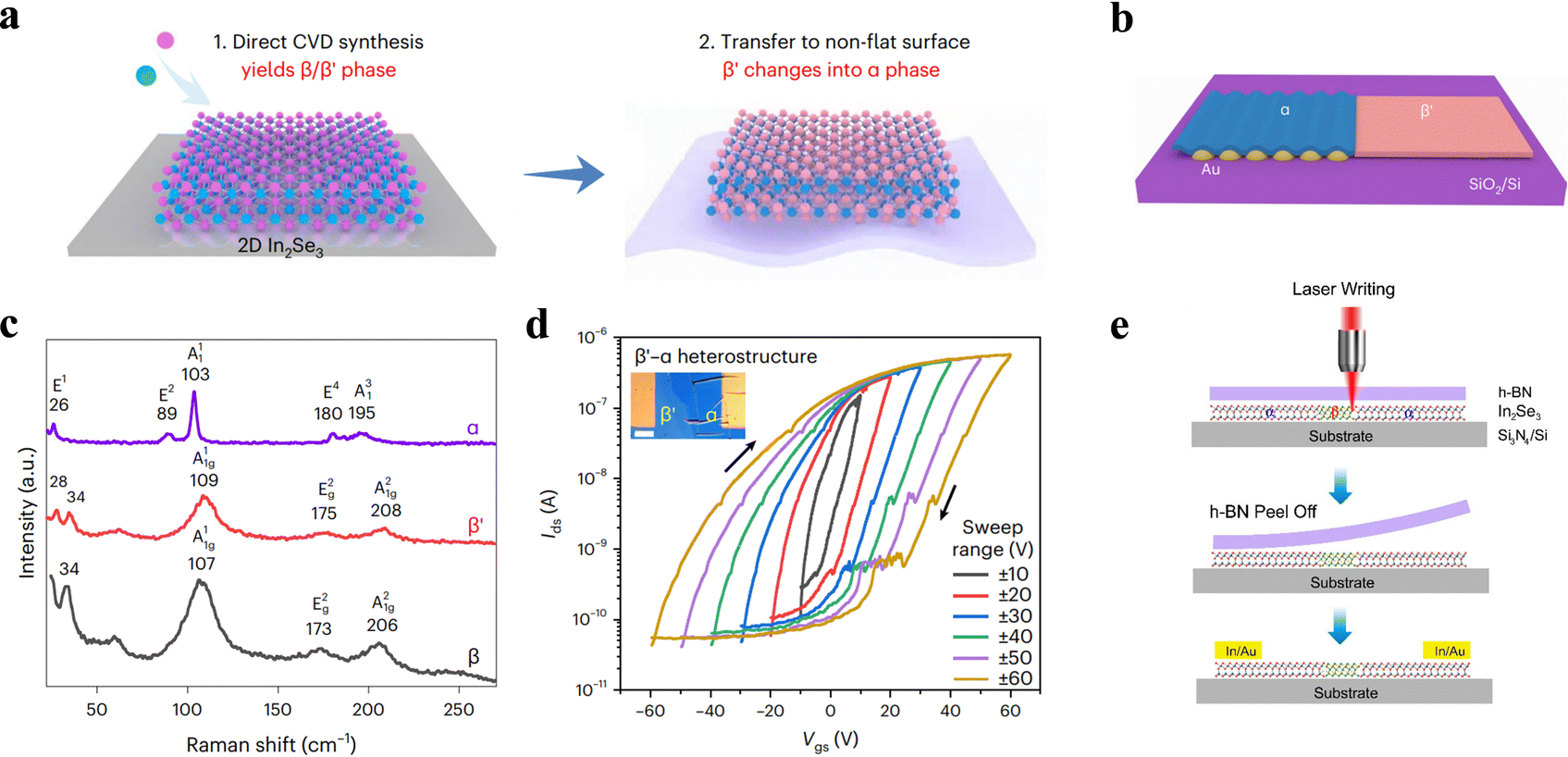 | ||
| Fig. 13 (a) Schematic of the controlled synthesis of β-, β′- and α-In2Se3 films. (b) Schematic of the α–β′ hetero-phase junction. (c) Raman spectra of β-, β′- and α-In2Se3. (d) Hysteresis transfer characteristic loops of α–β′ junction devices during double sweeping with various Vgs sweep ranges. (e) Schematic direct-laser-writing procedure.130,159 Reprinted with permission from ref. 130. Copyright 2022, The Author, under exclusive license to springer Nature limited. Reprinted with permission from ref. 159. Copyright 2019 American Chemical Society. | ||
Similarly, Igo et al. fabricated β–α In2Se3 hetero-phase junctions utilizing laser writing which demonstrate rectifying electrical behaviors and short-circuit photocurrent, indicating potential applications as ultrathin nanoscale photodiodes and photovoltaics, which are shown in Fig. 13e.159 Li et al. developed a vdW heterophase homojunction and tuned the electronic characteristics between n-type α-phase and p-type β-phase semiconductors by alloying Sb into In2Se3 and controlling the Sb concentration. This structure exhibited excellent broadband photovoltaic performance,160 high open circuit voltage (∼400 mV), a high on/off current ratio (∼106), and a high-speed response time (∼102 μs), with reconfigurable performance via polarization switching. These studies undoubtedly inspire the idea that by combining the correlated phases and ferroelectric (FE) properties of In2Se3, along with the realized polarizable hetero-phase junction, numerous opportunities can be opened up in developing novel structures and concepts for future FE electronics as well as logic-in-memory devices.159
6.2 Phase change memory
Phase change memory (PCM) is another important application of the crystalline–crystalline phase transitions.161–164 Reversible polymorphic layered materials provide an alternative atomic transition mechanism for low-energy electronic and photonic nonvolatile memories. Previously, Ge2Sb2Te was commonly utilized as the phase change material for PCM, achieving the transition between amorphous and crystalline states through heating.165 However, this process consumed a significant amount of energy and led to a long response time for PCM. In contrast, In2Se3, with its non-melting phase transition, can effectively reduce the phase transition temperature and set/reset time which are demonstrated in Fig. 14a, thereby achieving efficient and high-performance PCM.166,167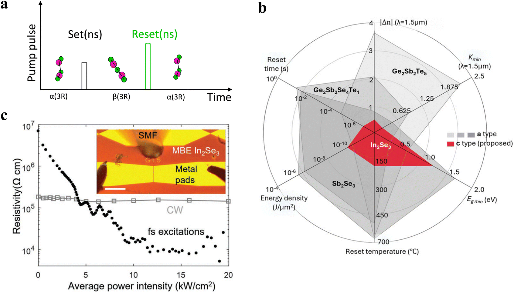 | ||
| Fig. 14 (a) Phase transition devices response. (b) Comparison of the performance matrix of PCMs between crystalline and amorphous states and a polymorphic layered In2Se3 (red part). (c) The In2Se3 phase change device: the relationship between resistance and excitation optical power at 1550 nm wavelength.43,168 Reprinted with permission from ref. 168. Copyright 2024 The Author, published by De Gruyter, Berlin/Boston. Reprinted with permission from ref. 43. Copyright 2022 Wiley-VCH GmbH. | ||
Moreover, Fig. 14b depicts the comparison of PCM performance among four commonly used PCM materials, further indicating the superior performance of In2Se3 in PCM.169–172 The optical transparency of In2Se3 in both states at telecommunication wavelengths guarantees low insertion loss, with both optical bandgaps of the material exceeding 0.8 eV, rendering it transparent.43 It is more worth mentioning that the refractive index change in layered In2Se3 is only half of that in Ge2Sb2Te5, a typical phase transition material used in PCM we mentioned before, but In2Se3's figure of merit as an optical phase change material is among the highest of all optical PCM materials.
Li et al. demonstrated that a single nanosecond pulse with nearly double the energy can switch the material from the β-state to the α-state,43 which is shown in Fig. 14a, and proved that the optical transparency of In2Se3 at telecommunication wavelengths enables low insertion loss and phase-only memory devices. Fig. 14c illustrates the relationship between device resistivity and light intensity at 1550 nm, further indicating the ability of In2Se3 to undergo phase transition under optical excitation, enabling PCM through resistivity changes. Choi et al. firstly reported a novel PCM using a layered crystalline In2Se3 film on a graphene bottom electrode,44 leveraging reversible phase changes between the crystalline β and γ phases for repeatable SET/RESET programming. The resulting change in configurational entropy is expected to be significantly smaller compared to the melting-induced RESET programming commonly seen in conventional In2Se3-based PCM. The unique phase change characteristics of polymorphic layered materials, specifically In2Se3, propel them to the forefront of future investigations aimed at developing photonic memory solutions that are energy-efficient, swift, and resilient.
6.3 Integrated photonic nonvolatile phase shifters
Light-sensitive phase-change materials are essential for integrated photonic devices as well. In2Se3, with its stable and tunable refractive index, exhibits excellent performance in nonvolatile phase shifters and post-fabrication phase trimming. This makes it highly valuable for photonic applications including programmable and reconfigurable photonic networks.173,174 Wu et al. integrated micro-ring resonators (MRRs) with multi-layer In2Se3 sheets,175 utilizing them as phase shifters. Fig. 15a shows the side view cartoon of atomic structures for α-In2Se3 and β′-In2Se3 that can be thermally driven. The Raman spectra of the α-In2Se3 flake at 20 °C before (α-In2Se3) and after (β′-In2Se3) thermal annealing in Fig. 15b further confirm the thermally driven reversible phase transitions between α and β′ phases. An optical microscope image of an MRR is shown in Fig. 15c. MMR is a type of ring-shaped resonant cavity that can achieve resonant amplification and filtering of light, and is widely used in optical sensors and communication systems. It is found that after thermal annealing at 300 °C, there is a red shift in the resonance wavelength from 1277.427 to 1277.470 nm, as depicted in Fig. 15d. This shift is attributed to the phase transition of In2Se3 from α to β′, with the refractive index of the material changing from 2.25 for α-In2Se3 to 2.47 for β′-In2Se3. This significant variation in refractive index plays a crucial role in integrated photonics applications.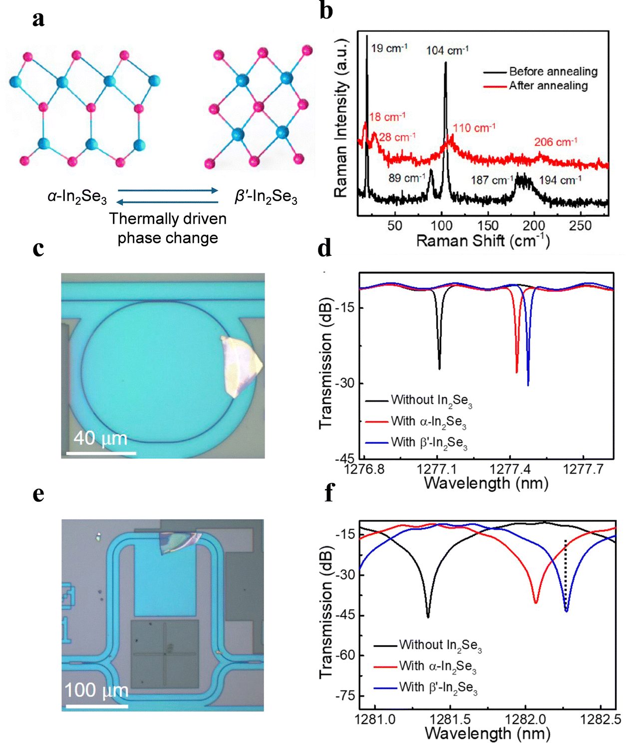 | ||
| Fig. 15 (a) Side-view cartoon of atomic structures for α-In2Se3 and β′-In2Se3. (b) Raman spectra of a 2H In2Se3 flake at 20 °C before (α-In2Se3) and after (β′-In2Se3) thermal annealing. (c) Optical microscope image of an MRR integrated with a 45 nm-thick In2Se3 flake. (d) Transmission spectra of the MRR (α and β′ phases). (e) Optical microscope image of an MZI integrated with a 90 nm-thick In2Se3. (f) Transmission spectra of the MZI (α and β′ phases).175 Reprinted with permission from ref. 175. Copyright 2023 American Chemical Society. | ||
The Mach–Zehnder interferometer (MZI) is widely used to measure optical path differences through interference effects. Its flexibility in terms of channel spacing and grid configuration makes it ideal for fabricating phase shifters, modulators, sensors, and other optical devices. Wu et al. integrated multilayer α-In2Se3 flakes into the MZI, with an optical image of the MZI shown in Fig. 15e.175 The extinction ratio (ER), which measures optical wave loss in materials, was evaluated experimentally.176 The original MZI exhibited an ER of approximately 34.1 dB, which decreased to 29.5 dB after integrating 90 nm thick α-In2Se3 flakes, and then increased to 32.6 dB following thermal annealing. This high ER indicates that multilayer In2Se3 is a low-loss optical material in the O-band. Additionally, a red shift of 206 pm was observed after thermal annealing, as shown in Fig. 15f. These results demonstrate the potential of utilizing In2Se3's phase-change properties in low-loss phase shifters.
Wang et al. developed a novel photonic PCM-enabled reversible metalens on a standard silicon photonic platform by employing a fixed geometric design.177 The unique refractive index combination of In2Se3 allows for nonvolatile tuning of the focusing length. These studies demonstrate the successful use of phase-change materials to achieve a tunable refractive index, which in turn facilitates the creation of photonic memory devices with reduced insertion loss and minimized power consumption. The layered In2Se3 prototype offers promising potential for integrated photonic devices, particularly in nonvolatile optical memory applications.43,175,176
7. Summary and outlook
This review examines the phase transitions in In2Se3, highlighting their fundamental properties and potential applications. These transitions significantly affect key material properties such as electrical resistance, photo-responsivity, thermal conductivity, and refractive index. The ability to control phase transitions through external factors like temperature, mechanical stress, and electric fields offers versatile control over the material's properties, enabling its use in reconfigurable applications such as homojunctions, optical modulators, and phase change materials. The review provides a comprehensive overview of In2Se3, focusing on its structural characteristics, methods of characterization, performance comparisons, and the conditions necessary for phase transitions. This detailed analysis aims to enhance understanding of In2Se3's phase transition behaviours and its potential for advancing future technologies.Looking ahead, several future research directions can further advance the understanding of In2Se3. First, phase stabilization techniques should be prioritized. This involves developing novel methods, such as the use of specific dopants or the exploration of external conditions like pressure and annealing, to stabilize the desired phases of In2Se3 at room temperature. A deep understanding of the thermodynamic and kinetic factors involved is essential for improving device reliability by minimizing performance-degrading phase transitions. Second, layer engineering deserves attention. Investigating the effects of different layer stacking sequences and intercalation techniques on In2Se3 properties, with a focus on addressing growth-related challenges like precise control over layer numbers and phase uniformity can enable the tuning of bandgaps and carrier mobility for specific applications. This approach could lead to more efficient and versatile device designs by allowing for tailored responses to external stimuli. Crucially, we must prioritize the resolution of growth-related bottlenecks, such as precise layer number control in large-area samples and uniformity of phase distribution, while addressing cost, environmental sustainability, and process consistency for industrial scalability. Third, integration with other materials warrants further exploration. Examining the interfacial properties and electronic coupling when combining In2Se3 with other two-dimensional materials can enhance charge transfer and other critical characteristics. Optimizing heterostructure designs can facilitate the development of innovative, high-performance electronic and optoelectronic components. Finally, addressing the challenges of scaling up high-quality In2Se3 synthesis is crucial. It is important to tackle issues related to cost, uniformity, and environmental impact. Developing cost-effective methods, optimizing processes for consistency, and adopting sustainable practices will be essential for industrial applications of this material.
Author contributions
W. Liao proposed and supervised the project. W. Zheng wrote the manuscript with comments from W. Liao, Z. Liu, T. Liu, D. Wang, and L. Wang. All authors discussed the results and commented on the manuscript.Data availability
No primary research results, software or code have been included and no new data were generated or analysed as part of this review.Conflicts of interest
The authors declare no competing interests.Acknowledgements
The work was partially supported by the financial support from the Guangdong Basic and Applied Basic Research Foundation (Grant No. 2023A1515010693), partially by the Shenzhen Science and Technology Program (Grant No. ZDSYS20220527171402005), the Shenzhen University 2035 Program for Excellent Research (Grant No. 2023C008), the Shenzhen Strategic Emerging Industry Support Plan (Grant NO. F-2023-Z99-509043), and the National Natural Science Foundation of China (Grant No. 61904110 and No. 52302187). The authors also acknowledge the support from the Instrumental Analysis Center of Shenzhen University (Xili Campus).References
- W. Liao, S. Zhao, F. Li, C. Wang, Y. Ge, H. Wang, S. Wang and H. Zhang, Nanoscale Horiz., 2020, 5, 787–807 RSC.
- Z. Lin, A. McCreary, N. Briggs, S. Subramanian, K. Zhang, Y. Sun, X. Li, N. J. Borys, H. Yuan and S. K. Fullerton-Shirey, 2D Mater., 2016, 3, 042001 CrossRef.
- S. Das, M. Kim, J.-W. Lee and W. Choi, Crit. Rev. Solid State Mater. Sci., 2014, 39, 231–252 CrossRef CAS.
- B. Lv, Z. Yan, W. Xue, R. Yang, J. Li, W. Ci, R. Pang, P. Zhou, G. Liu and Z. Liu, Mater. Horiz., 2021, 8, 1472–1480 RSC.
- B. Lv, W. Xue, Z. Yan, R. Yang, H. Wu, P. Wang, Y. Zhang, J. Hou, W. Zhu and X. Xu, Sci. China Mater., 2022, 65, 1639–1645 CrossRef CAS.
- X. Qian, J. Liu, L. Fu and J. Li, Science, 2014, 346, 1344–1347 CrossRef CAS PubMed.
- Z. Lin, C. Wang and Y. Chai, Small, 2020, 16, 2003319 CrossRef CAS PubMed.
- H. Jiang, L. Zheng, Z. Liu and X. Wang, InfoMat, 2020, 2, 1077–1094 CrossRef CAS.
- J. Du, H. Yu, B. Liu, M. Hong, Q. Liao, Z. Zhang and Y. Zhang, Small Methods, 2021, 5, 2000919 CrossRef CAS.
- S. J. Kim, K. Choi, B. Lee, Y. Kim and B. H. Hong, Annu. Rev. Mater. Res., 2015, 45, 63–84 CrossRef CAS.
- Y. Guo, C. Liu, Q. Yin, C. Wei, S. Lin, T. B. Hoffman, Y. Zhao, J. Edgar, Q. Chen and S. P. Lau, ACS Nano, 2016, 10, 8980–8988 CrossRef CAS.
- Q. Ma, G. Ren, K. Xu and J. Z. Ou, Adv. Opt. Mater., 2021, 9, 2001313 CrossRef CAS.
- S. Yu, X. Wu, Y. Wang, X. Guo and L. Tong, Adv. Mater., 2017, 29, 1606128 CrossRef PubMed.
- Q. Li, J. Lu, P. Gupta and M. Qiu, Adv. Opt. Mater., 2019, 7, 1900595 CrossRef CAS.
- F. Zhou, J. Chen, X. Tao, X. Wang and Y. Chai, Research, 2019, 1–17 CrossRef.
- X. Wang, Y. Sun and K. Liu, 2D Mater., 2019, 6, 042001 CrossRef CAS.
- P. Hess, Nanoscale Horiz., 2021, 6, 856–892 RSC.
- G. Hussain, M. Asghar, M. W. Iqbal, H. Ullah and C. Autieri, Appl. Surf. Sci., 2022, 590, 153131 CrossRef CAS.
- W. Eerenstein, N. Mathur and J. F. Scott, Nature, 2006, 442, 759–765 CrossRef CAS.
- W. Li, X. Qian and J. Li, Nat. Rev. Mater., 2021, 6, 829–846 CrossRef CAS.
- X. Yin, C. S. Tang, Y. Zheng, J. Gao, J. Wu, H. Zhang, M. Chhowalla, W. Chen and A. T. Wee, Chem. Soc. Rev., 2021, 50, 10087–10115 RSC.
- M. Si, Z. Zhang, S.-C. Chang, N. Haratipour, D. Zheng, J. Li, U. E. Avci and P. D. Ye, ACS Nano, 2021, 15, 5689–5695 CrossRef CAS.
- A. K. Saha, M. Si, P. D. Ye and S. K. Gupta, Appl. Phys. Lett., 2020, 117, 183504 CrossRef CAS.
- S. Manzeli, D. Ovchinnikov, D. Pasquier, O. V. Yazyev and A. Kis, Nat. Rev. Mater., 2017, 2, 1–15 Search PubMed.
- J. Van Landuyt, G. Van Tendeloo and S. Amelinckx, Phys. Status Solidi, 1975, 30, 299–314 CrossRef CAS.
- Y. Kou, L. Chen, J. Mu, H. Miao, Y. Wang, X. Hu and F. Teng, Nanotechnology, 2020, 31, 195601 CrossRef CAS PubMed.
- M. Rajapakse, B. Karki, U. O. Abu, S. Pishgar, M. R. K. Musa, S. S. Riyadh, M. Yu, G. Sumanasekera and J. B. Jasinski, npj 2D Mater. Appl., 2021, 5, 30 CrossRef CAS.
- H. Yang, S. W. Kim, M. Chhowalla and Y. H. Lee, Nat. Phys., 2017, 13, 931–937 Search PubMed.
- D. A. Rehn, Y. Li, E. Pop and E. J. Reed, npj Comput. Mater., 2018, 4, 2 Search PubMed.
- J. Li, H. Li, X. Niu and Z. Wang, ACS Nano, 2021, 15, 18683–18707 CrossRef CAS PubMed.
- W. Ding, J. Zhu, Z. Wang, Y. Gao, D. Xiao, Y. Gu, Z. Zhang and W. Zhu, Nat. Commun., 2017, 8, 14956 CrossRef CAS PubMed.
- M. Küpers, P. M. Konze, A. Meledin, J. Mayer, U. Englert, M. Wuttig and R. Dronskowski, Inorg. Chem., 2018, 57, 11775–11781 CrossRef PubMed.
- Z. Yang, W. Jie, C.-H. Mak, S. Lin, H. Lin, X. Yang, F. Yan, S. P. Lau and J. Hao, ACS Nano, 2017, 11, 4225–4236 CrossRef CAS PubMed.
- S. Mueller, S. R. Summerfelt, J. Muller, U. Schroeder and T. Mikolajick, IEEE Electron Device Lett., 2012, 33, 1300–1302 CAS.
- M. H. Park, H. J. Kim, Y. J. Kim, T. Moon, K. D. Kim and C. S. Hwang, Nano Energy, 2015, 12, 131–140 CrossRef CAS.
- Z. Zheng, J. Yao and G. Yang, J. Mater. Chem. C, 2016, 4, 8094–8103 RSC.
- C. Zhou and Y. Chai, Adv. Electron. Mater., 2017, 3, 1600400 CrossRef.
- S. Wang, L. Liu, L. Gan, H. Chen, X. Hou, Y. Ding, S. Ma, D. W. Zhang and P. Zhou, Nat. Commun., 2021, 12, 53 CrossRef CAS PubMed.
- L. Wang, X. Wang, Y. Zhang, R. Li, T. Ma, K. Leng, Z. Chen, I. Abdelwahab and K. P. Loh, Adv. Funct. Mater., 2020, 30, 2004609 CrossRef CAS.
- M. Si, A. K. Saha, S. Gao, G. Qiu, J. Qin, Y. Duan, J. Jian, C. Niu, H. Wang and W. Wu, Nat. Electron., 2019, 2, 580–586 CrossRef CAS.
- C. Xu, J. Mao, X. Guo, S. Yan, Y. Chen, T. W. Lo, C. Chen, D. Lei, X. Luo and J. Hao, Nat. Commun., 2021, 12, 3665 CrossRef CAS PubMed.
- F. Lyu, X. Li, J. Tian, Z. Li, B. Liu and Q. Chen, ACS Appl. Mater. Interfaces, 2022, 14, 23637–23644 CrossRef CAS PubMed.
- T. Li, Y. Wang, W. Li, D. Mao, C. J. Benmore, I. Evangelista, H. Xing, Q. Li, F. Wang and G. Sivaraman, Adv. Mater., 2022, 34, 2108261 CrossRef CAS PubMed.
- M. S. Choi, B. K. Cheong, C. H. Ra, S. Lee, J. H. Bae, S. Lee, G. D. Lee, C. W. Yang, J. Hone and W. J. Yoo, Adv. Mater., 2017, 29, 1703568 CrossRef PubMed.
- D. Kang, T. Rim, C.-K. Baek, M. Meyyappan and J.-S. Lee, Appl. Phys. Lett., 2013, 103, 233504 CrossRef.
- Z. Li, Y. Lv, L. Ren, J. Li, L. Kong, Y. Zeng, Q. Tao, R. Wu, H. Ma and B. Zhao, Nat. Commun., 2020, 11, 1151 CrossRef CAS PubMed.
- M. Hÿtch, E. Snoeck and R. Kilaas, Ultramicroscopy, 1998, 74, 131–146 CrossRef.
- R. Vilaplana, S. G. Parra, A. Jorge-Montero, P. Rodríguez-Hernández, A. Munoz, D. Errandonea, A. Segura and F. J. Manjón, Inorg. Chem., 2018, 57, 8241–8252 CrossRef CAS.
- S. Wan, Q. Peng, Z. Wu and Y. Zhou, Appl. Phys. Lett., 2022, 14, 25693–25700 CAS.
- J.-K. Qin, C. Wang, L. Zhen, L.-J. Li, C.-Y. Xu and Y. Chai, Prog. Mater. Sci., 2021, 122, 100856 CrossRef CAS.
- W. Liao, Y. Huang, H. Wang and H. Zhang, Appl. Mater. Today, 2019, 16, 435–455 CrossRef.
- H. Jiao, X. Wang, S. Wu, Y. Chen, J. Chu and J. Wang, Appl. Phys. Rev., 2023, 10, 011310 CAS.
- B. Tang, L. Hou, M. Sun, F. Lv, J. Liao, W. Ji and Q. Chen, Nanoscale, 2019, 11, 12817–12828 RSC.
- X. Jiang, Y. Feng, K.-Q. Chen and L.-M. Tang, J. Phys.: Condens. Matter, 2019, 32, 105501 CrossRef PubMed.
- S. He, D. Zou and Y.-Q. Zhao, Curr. Appl. Phys., 2024, 59, 122–128 CrossRef.
- Y. Zheng, H. Ravichandran, T. F. Schranghamer, N. Trainor, J. M. Redwing and S. Das, Nat. Commun., 2022, 13, 5578 CrossRef CAS PubMed.
- S. Mukherjee and E. Koren, Isr. J. Chem., 2022, 62, e202100112 CrossRef CAS.
- K.-H. Kim, I. Karpov, R. H. Olsson III and D. Jariwala, Nat. Nanotechnol., 2023, 18, 1–20 CrossRef PubMed.
- H. Chen, X. Xue, C. Liu, J. Fang, Z. Wang, J. Wang, D. W. Zhang, W. Hu and P. Zhou, Nat. Electron., 2021, 4, 399–404 CrossRef CAS.
- W. Huh, D. Lee and C. H. Lee, Adv. Mater., 2020, 32, 2002092 CrossRef CAS PubMed.
- L. W. Martin and A. M. Rappe, Adv. Opt. Mater., 2016, 2, 1–14 Search PubMed.
- Y. Hu, W. Feng, M. Dai, H. Yang, X. Chen, G. Liu, S. Zhang and P. Hu, Semicond. Sci. Technol., 2018, 33, 125002 CrossRef.
- W. F. Io, S. Yuan, S. Y. Pang, L. W. Wong, J. Zhao and J. Hao, Nano Res., 2020, 13, 1897–1902 CrossRef CAS.
- C. P. Hsu, A. Useinov, W. Y. Woon, S. Liao and T. H. Hou, Adv. Electron. Mater., 2024, 10, 2300880 CrossRef CAS.
- H. Bergeron, D. Lebedev and M. C. Hersam, Chem. Rev., 2021, 121, 2713–2775 CrossRef CAS PubMed.
- S. Popović, A. Tonejc, B. Gržeta-Plenković, B. Čelustka and R. Trojko, J. Appl. Crystallogr., 1979, 12, 416–420 CrossRef.
- K. Osamura, Y. Murakami and Y. Tomiie, J. Phys. Soc. Jpn., 1966, 21, 1848 CrossRef CAS.
- Z. Chen, W. Fu, L. Wang, W. Yu, H. Li, C. K. Y. Tan, I. Abdelwahab, Y. Shao, C. Su and M. Sun, Adv. Sci., 2021, 8, 2100713 CrossRef CAS PubMed.
- J. Jasinski, W. Swider, J. Washburn, Z. Liliental-Weber, A. Chaiken, K. Nauka, G. Gibson and C. Yang, Appl. Phys. Lett., 2002, 81, 4356–4358 CrossRef CAS.
- N. Balakrishnan, E. D. Steer, E. F. Smith, Z. R. Kudrynskyi, Z. D. Kovalyuk, L. Eaves, A. Patanè and P. H. Beton, 2D Mater., 2018, 5, 035026 CrossRef.
- Q. Hao, H. Yi, H. Su, B. Wei, Z. Wang, Z. Lao, Y. Chai, Z. Wang, C. Jin and J. Dai, Nano Lett., 2019, 19, 2634–2640 CrossRef CAS PubMed.
- Q. Meng, F. Yu, G. Liu, J. Zong, Q. Tian, K. Wang, X. Qiu, C. Wang, X. Xi and Y. Zhang, Nanomaterials, 2023, 13, 1533 CrossRef CAS PubMed.
- C. K. Y. Tan, W. Fu and K. P. Loh, Chem. Rev., 2023, 123, 8701–8717 CrossRef CAS PubMed.
- L. Wang, X. Zhou, M. Su, Y. Zhang, R. Li, R. Zhang, X. Wu, Z. Wu, W. P. D. Wong and Q.-H. Xu, ACS Nano, 2023, 18, 809–818 CrossRef PubMed.
- T. Lim, J. H. Lee, D. Kim, J. Bae, S. Jung, S. M. Yang, J. I. Jang and J. Jang, Adv. Mater., 2024, 36, 2308301 CrossRef CAS PubMed.
- K. Ueda, R. Murata, T. Sasagawa and Y. Shiomi, Jpn. J. Appl. Phys., 2023, 62, 061006 CrossRef CAS.
- J. Y. Jiping Ye, S. S. Sigeo Soeda, Y. N. Yoshio Nakamura and O. N. Osamu Nittono, Jpn. J. Appl. Phys., 1998, 37, 4264 CrossRef.
- J. Xiao, H. Zhu, Y. Wang, W. Feng, Y. Hu, A. Dasgupta, Y. Han, Y. Wang, D. A. Muller, L. W. Martin, P. Hu and X. Zhang, Phys. Rev. Lett., 2018, 120, 227601 CrossRef CAS PubMed.
- W. Feng, F. Gao, Y. Hu, M. Dai, H. Liu, L. Wang and P. Hu, ACS Appl. Mater. Interfaces, 2018, 10, 27584–27588 CrossRef CAS PubMed.
- A. F. Qasrawi, Thin Solid Films, 2006, 514, 267–271 CrossRef CAS.
- C. Julien, M. Eddrief, K. Kambas and M. Balkanski, Thin Solid Films, 1986, 137, 27–37 CrossRef CAS.
- G. Almeida, S. Dogan, G. Bertoni, C. Giannini, R. Gaspari, S. Perissinotto, R. Krahne, S. Ghosh and L. Manna, J. Am. Chem. Soc., 2017, 139, 3005–3011 CrossRef CAS PubMed.
- Z. Zou, D. Li, J. Liang, X. Zhang, H. Liu, C. Zhu, X. Yang, L. Li, B. Zheng, X. Sun, Z. Zeng, J. Yi, X. Zhuang, X. Wang and A. Pan, Nanoscale, 2020, 12, 6480–6488, 10.1039/C9NR10387B.
- J. Quereda, R. Biele, G. Rubio-Bollinger, N. Agraït, R. D'Agosta and A. Castellanos-Gomez, Adv. Opt. Mater., 2016, 4, 1939–1943 CrossRef CAS.
- X. Tao and Y. Gu, Nano Lett., 2013, 13, 3501–3505 CrossRef CAS PubMed.
- Q. Wang, L. Yang, S. Zhou, X. Ye, Z. Wang, W. Zhu, M. D. McCluskey and Y. Gu, J. Phys. Chem. Lett., 2017, 8, 2887–2894 CrossRef CAS PubMed.
- J. L. Collins, C. Wang, A. Tadich, Y. Yin, C. Zheng, J. Hellerstedt, A. Grubišić-Čabo, S. Tang, S.-K. Mo, J. Riley, E. Huwald, N. V. Medhekar, M. S. Fuhrer and M. T. Edmonds, ACS Appl. Electron. Mater., 2020, 2, 213–219 CrossRef CAS.
- N. Balakrishnan, E. D. Steer, E. F. Smith, Z. R. Kudrynskyi, Z. D. Kovalyuk, L. Eaves, A. Patanè and P. H. Beton, 2D Mater., 2018, 5, 035026 CrossRef.
- J. Cui, H. Peng, Z. Song, Z. Du, Y. Chao and G. Chen, Chem. Mater., 2017, 29, 7467–7474 CrossRef CAS.
- W. Han, Z. Wang, S. Guan, J. Wei, Y. Jiang, L. Zeng, L. Shen, D. Yang and H. Wang, Appl. Phys. Rev., 2024, 11, 021314 CAS.
- Z. Zhang, L. Shi, B. Wang, J. Qu, X. Wang, T. Wang, Q. Jiang, W. Xue and X. Xu, Chin. Chem. Lett., 2024, 109687 Search PubMed.
- S. Mukherjee, D. Dutta, P. K. Mohapatra, L. Dezanashvili, A. Ismach and E. Koren, ACS Nano, 2020, 14, 17543–17553 CrossRef CAS PubMed.
- L. Liu, J. Dong, J. Huang, A. Nie, K. Zhai, J. Xiang, B. Wang, F. Wen, C. Mu and Z. Zhao, Chem. Mater., 2019, 31, 10143–10149 CrossRef CAS.
- S.-K. Wu, H.-J. Wang, S.-W. Hsiao, J.-S. Huang, W.-C. Chou, C.-S. Yang, S.-J. Chang, C.-H. Wu and Y.-C. Huang, ACS Appl. Nano Mater., 2024, 7, 20445–20453 CrossRef CAS.
- S. M. Poh, S. J. R. Tan, H. Wang, P. Song, I. H. Abidi, X. Zhao, J. Dan, J. Chen, Z. Luo, S. J. Pennycook, A. H. Castro Neto and K. P. Loh, Nano Lett., 2018, 18, 6340–6346 CrossRef CAS PubMed.
- Chanchal, K. Jindal, A. Pandey, M. Tomar and P. K. Jha, Appl. Surf. Sci., 2022, 595, 153505 CrossRef CAS.
- D. Wu, A. J. Pak, Y. Liu, Y. Zhou, X. Wu, Y. Zhu, M. Lin, Y. Han, Y. Ren and H. Peng, Nano Lett., 2015, 15, 8136–8140 CrossRef CAS PubMed.
- J. O. Island, S. I. Blanter, M. Buscema, H. S. J. van der Zant and A. Castellanos-Gomez, Nano Lett., 2015, 15, 7853–7858 CrossRef CAS PubMed.
- D. Dutta, S. Mukherjee, M. Uzhansky and E. Koren, npj 2D Mater. Appl., 2021, 5, 81 CrossRef CAS.
- Y. Li, C. Chen, W. Li, X. Mao, H. Liu, J. Xiang, A. Nie, Z. Liu, W. Zhu and H. Zeng, Adv. Electron. Mater., 2020, 6, 2000061 CrossRef CAS.
- Y. Huang, E. Sutter, N. N. Shi, J. Zheng, T. Yang, D. Englund, H.-J. Gao and P. Sutter, ACS Nano, 2015, 9, 10612–10620 CrossRef CAS PubMed.
- R. B. Jacobs-Gedrim, M. Shanmugam, N. Jain, C. A. Durcan, M. T. Murphy, T. M. Murray, R. J. Matyi, R. L. Moore and B. Yu, ACS Nano, 2014, 8, 514–521 CrossRef CAS PubMed.
- C. Jeengar, K. Jindal, M. Tomar and P. K. Jha, J. Electron. Mater., 2025, 54, 3553–3559 CrossRef CAS.
- Z. Q. Zheng, J. D. Yao and G. W. Yang, J. Mater. Chem. C, 2016, 4, 8094–8103 RSC.
- J. Shin, J. Jang, C. H. Choi, J. Kim, L. Eddy, P. Scotland, L. W. Martin, Y. Han and J. M. Tour, Adv. Electron. Mater., 2024, 2400603 CrossRef.
- D. H. Seo, J. W. Kim, J.-H. Seong, H.-C. Lee, S.-I. Kim and T. Kim, Electron. Mater. Lett., 2023, 20, 192–198 CrossRef.
- C. Chen, M. Dai, C. Xu, X. Che, C. Dwyer, X. Luo and Y. Zhu, Nano Lett., 2024, 24, 1539–1543 CrossRef CAS PubMed.
- F. Xue, W. Hu, K. C. Lee, L. S. Lu, J. Zhang, H. L. Tang, A. Han, W. T. Hsu, S. Tu and W. H. Chang, Adv. Funct. Mater., 2018, 28, 1803738 CrossRef.
- H. Guo, Y. Xia, Y. Yu, R. Zhou, H. Niu, X. Mao, L. Wan and J. Xu, Mater. Sci. Semicond. Process., 2022, 138, 106304 CrossRef CAS.
- S. V. Solanke, R. Soman, M. Rangarajan, S. Raghavan and D. N. Nath, Sens. Actuators, A, 2021, 317, 112455 CrossRef CAS.
- N. Mohta, A. Rao, P. Suri and D. N. Nath, Semicond. Sci. Technol., 2023, 38, 095008 CrossRef CAS.
- Y. Zhou, D. Wu, Y. Zhu, Y. Cho, Q. He, X. Yang, K. Herrera, Z. Chu, Y. Han and M. C. Downer, Nano Lett., 2017, 17, 5508–5513 CrossRef CAS PubMed.
- L. Wang, H. Chen, M. F. Chen, Y. F. Long, K. Liu and K. P. Loh, Adv. Funct. Mater., 2024, 34, 2316583 CrossRef CAS.
- N. Balakrishnan, C. R. Staddon, E. F. Smith, J. Stec, D. Gay, G. W. Mudd, O. Makarovsky, Z. R. Kudrynskyi, Z. D. Kovalyuk and L. Eaves, 2D Mater., 2016, 3, 025030 CrossRef.
- X. Zheng, W. Han, K. Yang, L. W. Wong, C. S. Tsang, K. H. Lai, F. Zheng, T. Yang, S. P. Lau and T. H. Ly, Sci. Adv., 2022, 8, eabo0773 CrossRef CAS PubMed.
- C. Cui, W.-J. Hu, X. Yan, C. Addiego, W. Gao, Y. Wang, Z. Wang, L. Li, Y. Cheng, P. Li, X. Zhang, H. N. Alshareef, T. Wu, W. Zhu, X. Pan and L.-J. Li, Nano Lett., 2018, 18, 1253–1258 CrossRef CAS PubMed.
- M. W. Si, A. K. Saha, S. J. Gao, G. Qiu, J. K. Qin, Y. Q. Duan, J. Jian, C. Niu, H. Y. Wang, W. Z. Wu, S. K. Gupta and P. D. D. Ye, Nat. Electron., 2019, 2, 580–586 CrossRef CAS.
- R. Rashid, F. C.-C. Ling, S.-P. Wang, K. Xiao, X. Cui, Q. Rao and D.-K. Ki, J. Alloys Compd., 2021, 870, 159344 CrossRef CAS.
- S. Yan, C. Xu, C. Zhong, Y. Chen, X. Che, X. Luo and Y. Zhu, Angew. Chem., Int. Ed., 2023, 62, e202300302 CrossRef CAS PubMed.
- S. Wan, Y. Li, W. Li, X. Mao, C. Wang, C. Chen, J. Dong, A. Nie, J. Xiang and Z. Liu, Adv. Funct. Mater., 2019, 29, 1808606 CrossRef.
- L. Bai, C. Ke, Z. Luo, T. Zhu, L. You and S. Liu, ACS Nano, 2024, 18, 26103–26114 CAS.
- C. Xu, Y. Chen, X. Cai, A. Meingast, X. Guo, F. Wang, Z. Lin, T. W. Lo, C. Maunders and S. Lazar, Phys. Rev. Lett., 2020, 125, 047601 CrossRef CAS PubMed.
- C. Zheng, L. Yu, L. Zhu, J. L. Collins, D. Kim, Y. Lou, C. Xu, M. Li, Z. Wei and Y. Zhang, Sci. Adv., 2018, 4, eaar7720 CrossRef PubMed.
- M. Wu, Y. Xiao, Y. Zeng, Y. Zhou, X. Zeng, L. Zhang and W. Liao, InfoMat, 2021, 3, 362–396 CrossRef CAS.
- K. Liu, T. Zhang, B. Dang, L. Bao, L. Xu, C. Cheng, Z. Yang, R. Huang and Y. Yang, Nat. Electron., 2022, 5, 761–773 CrossRef CAS.
- C. Jia, S. Wu, J. Fan, C. Luo, M. Fan, M. Li, L. He, Y. Yang and H. Zhang, ACS Nano, 2023, 17, 6534–6544 CrossRef CAS PubMed.
- Z. Zheng, J. Yao, B. Wang, Y. Yang, G. Yang and J. Li, ACS Appl. Mater. Interfaces, 2017, 9, 43830–43837 CrossRef CAS PubMed.
- S. Chen, X. Liu, X. Qiao, X. Wan, K. Shehzad, X. Zhang, Y. Xu and X. Fan, Small, 2017, 13, 1604033 CrossRef PubMed.
- W. Zhang, Q. Su, B. Zhang, J. Peng and Y. Li, ACS Appl. Nano Mater., 2023, 6, 8795–8803 CrossRef CAS.
- W. Han, X. Zheng, K. Yang, C. S. Tsang, F. Zheng, L. W. Wong, K. H. Lai, T. Yang, Q. Wei and M. Li, Nat. Nanotechnol., 2023, 18, 55–63 CrossRef CAS PubMed.
- J. L. Collins, C. Wang, A. Tadich, Y. Yin, C. Zheng, J. Hellerstedt, A. Grubisic-Cabo, S. Tang, S.-K. Mo and J. Riley, ACS Appl. Electron. Mater., 2020, 2, 213–219 CrossRef CAS.
- W. Li, F. P. Sabino, F. Crasto de Lima, T. Wang, R. H. Miwa and A. Janotti, Phys. Rev. B, 2018, 98, 165134 CrossRef CAS.
- M. Buscema, G. A. Steele, H. S. J. Van Der Zant and A. Castellanos-Gomez, Nano Res., 2014, 7, 561–571 CrossRef.
- C.-H. Ho and Y.-C. Chen, RSC Adv., 2013, 3, 24896–24899 RSC.
- J. Tauc, R. Grigorovici and A. Vancu, Phys. Status Solidi B, 1966, 15, 627–637 CrossRef CAS.
- S. Fan, Q. A. Vu, S. Lee, T. L. Phan, G. Han, Y.-M. Kim, W. J. Yu and Y. H. Lee, ACS Nano, 2019, 13, 8193–8201 CrossRef CAS PubMed.
- S. Rolf-Pissarczyk, S. Yan, L. Malavolti, J. A. J. Burgess, G. McMurtrie and S. Loth, Phys. Rev. Lett., 2017, 119, 217201 CrossRef PubMed.
- Z. Chen, M. Sun, H. Li, B. Huang and K. P. Loh, Nano Lett., 2023, 23, 1077–1084 CrossRef CAS PubMed.
- M. Osman, Y. Huang, W. Feng, G. Liu, Y. Qiu and P. Hu, RSC Adv., 2016, 6, 70452–70459 RSC.
- Y. Hu, W. Feng, M. Dai, H. Yang, X. Chen, G. Liu, S. Zhang and P. Hu, Semicond. Sci. Technol., 2018, 33, 125002 CrossRef.
- M. Eddrief, C. Julien, M. Balkanski and K. Kambas, Mater. Lett., 1984, 2, 432–436 CrossRef CAS.
- F. Zhang, Z. Wang, J. Dong, A. Nie, J. Xiang, W. Zhu, Z. Liu and C. Tao, ACS Nano, 2019, 13, 8004–8011 CrossRef CAS PubMed.
- S. Popovi, B. Elustka and D. Bidjin, Phys. Status Solidi A, 1971, 6, 301–304 CrossRef.
- H.-G. Kim, I.-S. Min and W.-T. Kim, Solid State Commun., 1987, 64, 819–822 CrossRef CAS.
- N. D. Ignacio, J. Fatheema, Y.-R. Jeon and D. Akinwande, Adv. Electron. Mater., 2024, 10, 2300457 CrossRef CAS.
- L.-W. Wong, L. Huang, F. Zheng, Q. H. Thi, J. Zhao, Q. Deng and T. H. Ly, Nat. Commun., 2020, 11, 3982 CrossRef CAS PubMed.
- Y. Wu, T. Zhang, D. Guo, B. Li, K. Pei, W. You, Y. Du, W. Xing, Y. Lai, W. Ji, Y. Zhao and R. Che, Nat. Commun., 2024, 15, 10481 CrossRef CAS PubMed.
- F. Ke, C. Liu, Y. Gao, J. Zhang, D. Tan, Y. Han, Y. Ma, J. Shu, W. Yang, B. Chen, H.-K. Mao, X.-J. Chen and C. Gao, Appl. Phys. Lett., 2014, 104, 212102 CrossRef.
- J. Zhao, L. Chen, B. Xu, B. Zheng, J. Fan and H. Xu, Phys. Rev. B, 2020, 101, 121407 CrossRef CAS.
- M. Wu, Z. Lou, C. M. Dai, T. Wang, J. Wang, Z. Zhu, Z. Xu, T. Sun, W. Li and X. Zheng, Adv. Mater., 2023, 35, 2300450 CrossRef CAS PubMed.
- J. Zhao and L. Yang, J. Phys. Chem. C, 2014, 118, 5445–5452 CrossRef CAS.
- A. M. Rasmussen, S. T. Teklemichael, E. Mafi, Y. Gu and M. D. McCluskey, Appl. Phys. Lett., 2013, 102, 062105 CrossRef.
- J. Liang, H. Jin, J. Zhang and X. Chen, Journal of Physics: Conference Series, IOP Publishing, 2020, vol. 1622, p. 012027 Search PubMed.
- A. M. Rasmussen, E. Mafi, W. Zhu, Y. Gu and M. D. McCluskey, Appl. Phys. Lett., 2016, 36, 549–556 CAS.
- G. Modi, S. K. Parate, C. Kwon, A. C. Meng, U. Khandelwal, A. Tullibilli, J. Horwath, P. K. Davies, E. A. Stach, J. Li, P. Nukala and R. Agarwal, Nature, 2024, 635, 847–853 CrossRef PubMed.
- J. Dong, L. Liu, A. Nie, J. Xiang, K. Zhai, B. Wang, F. Wen, C. Mu, Y. Chen and Z. Zhao, Appl. Phys. Lett., 2020, 116, 021602 CrossRef CAS.
- K. Yang, X. Li, C. Yu, D. Zeng, F. Chen, K. Zhang, W. Huang and H. Ji, Chin. J. Catal., 2019, 40, 796–818 CrossRef CAS.
- B. Liu and H.-M. Cheng, Nat. Nanotechnol., 2023, 18, 5–6 CrossRef CAS PubMed.
- J. Igo, M. Gabel, Z.-G. Yu, L. Yang and Y. Gu, ACS Appl. Nano Mater., 2019, 2, 6774–6782 CrossRef CAS.
- S. Li, B. Wang, L. Li, J. Li, M. Wang, G. Luo, X. Ren, Y. Yan and J. Li, Adv. Electron. Mater., 2022, 8, 2200665 CrossRef CAS.
- H.-S. P. Wong, S. Raoux, S. Kim, J. Liang, J. P. Reifenberg, B. Rajendran, M. Asheghi and K. E. Goodson, Proc. IEEE, 2010, 98, 2201–2227 Search PubMed.
- H. Lee, D.-H. Kang and L. Tran, Mater. Sci. Eng., B, 2005, 119, 196–201 CrossRef.
- H. Lee and D.-H. Kang, Jpn. J. Appl. Phys., 2005, 44, 4759 CrossRef CAS.
- S. Sourav, A. K. Dwivedi and A. Islam, J. Mater., 2016, 2016, 1–7 Search PubMed.
- M. Xu, X. Chen, Y. Guo, Y. Wang, D. Qiu, X. Du, Y. Cui, X. Wang and J. Xiong, Adv. Mater., 2023, 35, 2301063 CrossRef CAS PubMed.
- J. Zhou, Q. Zeng, D. Lv, L. Sun, L. Niu, W. Fu, F. Liu, Z. Shen, C. Jin and Z. Liu, Nano Lett., 2015, 15, 6400–6405 CrossRef CAS PubMed.
- G. Han, Z. G. Chen, J. Drennan and J. Zou, Small, 2014, 10, 2747–2765 CrossRef CAS PubMed.
- K. Ullah, Q. Li, T. Li and T. Gu, Nanophotonics, 2024, 13, 2089–2099 CrossRef CAS PubMed.
- M. Miscuglio, J. Meng, O. Yesiliurt, Y. Zhang, L. J. Prokopeva, A. Mehrabian, J. Hu, A. V. Kildishev and V. J. Sorger, 2020 International applied computational electromagnetics society symposium (aces), IEEE, 2020, pp. 1–3.
- A. Mavlonov, T. Razykov, F. Raziq, J. Gan, J. Chantana, Y. Kawano, T. Nishimura, H. Wei, A. Zakutayev and T. Minemoto, Sol. Energy, 2020, 201, 227–246 CrossRef CAS.
- M. J. Müller, A. Yadav, C. Persch, S. Wahl, F. Hoff and M. Wuttig, Adv. Electron. Mater., 2022, 8, 2100974 CrossRef.
- T. Kato and K. Tanaka, Jpn. J. Appl. Phys., 2005, 44, 7340 CrossRef CAS.
- W. Bogaerts, D. Pérez, J. Capmany, D. A. B. Miller, J. Poon, D. Englund, F. Morichetti and A. Melloni, Nature, 2020, 586, 207–216 CrossRef CAS PubMed.
- F. Ceccarelli, S. Atzeni, A. Prencipe, R. Farinaro and R. Osellame, J. Light Technol., 2019, 37, 4275–4281 CAS.
- J. Wu, Y. Ye, J. Jian, X. Yao, J. Li, B. Tang, H. Ma, M. Wei, W. Li and H. Lin, Nano Lett., 2023, 23, 6440–6448 CrossRef CAS PubMed.
- H. Li, Y. Anugrah, S. J. Koester and M. Li, Appl. Phys. Lett., 2012, 101, 111110 CrossRef.
- N. Wang, T. Li, B. Sun, Z. Wang, L. Zhou and T. Gu, Opt. Lett., 2021, 46, 4088–4091 CrossRef PubMed.
| This journal is © The Royal Society of Chemistry 2025 |