
Catalyst-assisted growth of CsPbBr3 perovskite nanowires†
Karam
Shreteh
 a,
Michael
Volokh
a and
Taleb
Mokari
*ab
a,
Michael
Volokh
a and
Taleb
Mokari
*ab
aDepartment of Chemistry, Ben-Gurion University of the Negev, Beer-Sheva, 8410501, Israel. E-mail: mokari@bgu.ac.il
bIlse Katz Institute for Nanoscale Science and Technology, Ben-Gurion University of the Negev, Beer-Sheva, 8410501, Israel
First published on 10th December 2024
Abstract
Halide perovskites (HPs), particularly at the nanoscale, attract attention due to their unique optical properties compared to other semiconductors. They exhibit bright emission, defect tolerance, and a broad tunable band gap. The ability to directly transport charge carriers along the HPs nanowires (NWs) has led to the development of methods for their synthesis. Most of these methods involve some version of an oriented attachment step with various modifications. In this study, we introduce CsPbBr3 nanowires produced via the solution–solid–solid (SSS) catalyst-assisted growth mechanism for the first time. We explored the kinetics of this process and examined the connection between the catalyst phase and its reactivity. We show how HP NWs grow with different SSS catalysts (i.e., Ag2S, Ag2Se, CuS) and discuss the required conditions for successful synthesis utilizing this mechanism. This method opens up a new avenue for producing HP NWs, which can be used to design and form new types of hybrid nanostructures.
Introduction
Halide perovskites (HPs) have been valued for their unique characteristics in various fields such as photovoltaics,1,2 optoelectronics,3,4 and catalysis.5,6 Lately, the study of quantum-confined colloidal HP nanocrystals has emerged as a significant area of research due to their defect tolerance,7 wide band gap tunability,8,9 and bright emission capabilities.9,10As with other semiconductors, the one-dimensional (1D) morphology has been the focus of many studies and applications. New methodologies for synthesizing crystalline HP nanowires (NWs) and nanorods have been developed, driven by the prospect of excellent charge carriers transport within such nanocrystals.11 For instance, Zhang et al. synthesized the first CsPbBr3 perovskite NWs with a diameter of about 10 nm;12 afterwards, through a stepwise purification process, they managed to reduce the diameter of these NWs to achieve strong quantum confinement at d ≈ 2 nm.13 Other homogeneous NWs with a tunable width were also prepared using short chain carboxylic acids and room temperature,11,14,15 or by harnessing the oriented attachment mechanism, where CsPbX3 (X = halide) cubes assemble to form the desired NW product.16–18 Due to the cubic nature of these materials, they do not prefer anisotropic growth, as known for wurtzite structures. The previously reported methods are based on the oriented attachment mechanism, where CsPbX3 cubes are attached to form 1D morphology; the synthetic tools that allow this process include low temperature, long time, and changing ligand concentration. However, the catalyst-assisted growth mechanism for growing perovskite nanowires has not yet been reported.
Herein, we describe the synthesis of CsPbBr3 nanowires via the solution–solid–solid (SSS) mechanism for the first time. We used semiconductor nanoparticles (Ag2S, Ag2Se, Cu2S) that undergo a phase transition to a superionic phase at the reaction temperature. This reactive phase is typically used as a catalyst for growing metal chalcogenides 1D nanocrystals.19–21 We succeeded in forming CsPbBr3 perovskite nanowires with μm length in very short synthesis times. Furthermore, we studied the formation kinetics and the effect of the catalyst's type, phase, and composition on the nanowires’ growth by real-time monitoring of phase transitions of the catalysts via in situ X-ray diffraction (XRD) in solution.
Preparing HPs using the SSS mechanism offers the benefit of catalyst-assisted growth, significantly improving synthesis time and reaction yield. The success of this approach suggests that other catalyst-assisted growth methods, such as solution–liquid–solid (SLS) and vapor–liquid–solid (VLS), could also be employed for HP formation. Notably, these methods are well-suited for large-scale nanowire synthesis, a key factor for advancing nanowire-based device manufacturing.22,23 Additionally, the flexibility of these catalytic routes holds great potential for developing hybrid nanostructures incorporating HPs, thereby broadening the scope of potential applications.24,25
Experimental section
Materials
All reactants and solvents were purchased from commercial sources and used as received unless indicated otherwise. Oleylamine (OAm, 98%), dodecanethiol (DDT, 98.5%), oleic acid (OA, 90%), octadecylamine (ODA, 90%), sulfur powder (S, 99.98%), and sodium diethyldithiocarbamate trihydrate (NadtcEt2·3H2O, ≥99.0%; abbreviated in the text as NadtcEt2 for simplicity) were purchased from Sigma-Aldrich. Octadecene (ODE, 90%) and anhydrous toluene (99.8%) were purchased from Alfa Aesar. Anhydrous copper(II) acetate (CuAc2, 97%), cesium carbonate (Cs2CO3, 99%), CdO powder (99.999%), and selenium powder (Se, 99.99%) were purchased from Strem. Lead bromide was purchased from Apollo Scientific Limited (PbBr, 99.999%). Silver nitrate (AgNO3, 99.8%) was purchased from Fisher Scientific. The solvents n-hexane (C6H14, 95%), toluene (C7H8, 99.7%), 2-propanol (IPA, 99.8%), and ethanol (EtOH, absolute, 99%) were purchased from Bio-Lab Chemicals, Israel.Synthetic procedures
![[thin space (1/6-em)]](https://www.rsc.org/images/entities/char_2009.gif) :1 molar ratio. After mixing, stirring, vacuum-filtration, and washing, chloroform was used for recrystallization.
:1 molar ratio. After mixing, stirring, vacuum-filtration, and washing, chloroform was used for recrystallization.
OAm, ODE, and OA were mixed under vacuum at 120 °C overnight before further use.
For the Cu2S-catalyzed CsPbBr3 NWs synthesis, we use a similar procedure, but with 220 °C reaction temperature and 0.2 mL Cu2S solution that was injected after the temperature raises back to the 220 °C setpoint after the OAm injection.
Characterization
Energy-dispersive X-ray spectroscopy (EDS) analysis was performed using a JEOL JEM-2100F TEM operated at 200 kV and equipped with an Oxford Instruments X-Max 65T SDD detector. The probe size during the analysis was set to 1 nm. AZtec software (v. 3.3) was used for the EDS data analysis.
High resolution STEM (HRSTEM) imaging was conducted using Spectra 200 (Thermo Fisher Scientific) with a Cs-corrected probe (S-CORR) scanning transmission electron microscope (S/TEM) operated at 200 kV. The images were recorded in STEM mode with a high-angle annular dark field (HAADF) detector.
Ex situ XRD measurements were conducted using Panalytical Empyrean III (Malvern Panalytical) multi-purpose diffractometer equipped with a Cu X-ray source (Cu Kα, λ = 1.5406 Å), operated at 45 kV and 40 mA. The instrument was equipped with the iCore–dCore automated XRD optics combination, a PixCEL 3D detector in 1D line-detector mode. Measurements were recorded of dry samples after drop-casting on (100) single-side polished Si substrates.
In situ XRD measurements were conducted using Panalytical Empyrean (Malvern Panalytical) diffractometer equipped with an X'Celerator detector using Cu Kα radiation (λ = 1.5406 Å), operated at 45 kV and 40 mA recording in Anton Paar's HTK 1200N high-temperature oven chamber with an aluminum oxide sample holder as a sample stage for continuous XRD monitoring at different temperatures. The chamber was filled with He(g) to maintain an inert atmosphere.
UV–vis absorption was measured using an Edinburgh Instruments DS5 dual beam spectrophotometer with tungsten halogen and deuterium light sources and quartz cuvettes with an optical path of 10 mm.
Photoluminescence (PL) spectra were collected using Varian Cary Eclipse fluorimeter, exciting the samples at λexc = 410 nm.
Results and discussion
The synthetic process commences by mixing PbBr2 powder and oleic acid in ODE. Following a purification step under vacuum at 120 °C (as detailed in Experimental section), oleylamine is added to the mixture. As the temperature rises to 190 °C, the mixture changes color to clear yellow due to the complexation of the PbBr2. Subsequently, Ag2S NPs (Fig. S1†) dispersion (see full details in the Experimental section) is injected, followed by the injection of a cesium oleate (Cs-OA) solution. After 5 minutes, thin (d ∼5 ± 1 nm, Fig. S2†) NWs with both spherical and cubic tips form, as depicted in the TEM image in Fig. 1a. EDS mapping (Fig. 1b and Fig. S2†) reveals that the spherical tips consist of silver (light blue) and sulfur (green), corresponding to the Ag2S NPs introduced during synthesis. Meanwhile, the NWs comprise cesium (yellow), lead (purple), and bromine (red).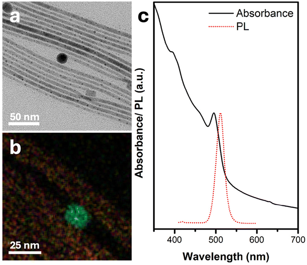 | ||
| Fig. 1 Characterization of Ag2S-catalyzed CsPbBr3 NWs. (a) TEM image, (b) elemental EDS map—silver in light blue, sulfur in green, cesium in yellow, lead in purple, and bromine in red, and (c) UV–vis absorbance and photoluminescence (PL) spectra in black dotted red lines, respectively (λexc = 410 nm). The dark field STEM image and individual elemental maps corresponding to panel (b) appear in Fig. S3.† | ||
The UV–vis absorbance spectrum in Fig. 1c exhibits a peak at 494 nm, characteristic of perovskite CsPbBr3 NWs, with a corresponding single PL emission peak centered about 511 nm.
Interestingly, although there are Ag2S NPs on the tip of each NW, their absorbance is not evident in the UV–vis spectrum. This discrepancy can be attributed to the negligible amount of Ag2S relative to the long CsPbBr3 NWs, which can reach lengths of 1–2 μm, as observed in the high-angle annular dark-field scanning transmission electron microscopy (HAADF-STEM) image in Fig. S4.† nanowires are shown in Fig. 2. The high-resolution TEM (HRTEM) image in Fig. 2a shows the NW's tip with a darker contrast, exhibiting the (122) and (102) crystallographic planes of monoclinic Ag2S. Further characterizations of the crystallographic structure of the nanowires are shown in Fig. 2. The NW, close to the interface with the Ag2S NP tip, shows a brighter contrast and displays the (101) planes of the cubic perovskite CsPbBr3 phase (d101 = 4.12 Å). The X-ray diffraction (XRD) pattern (Fig. 2b) corroborates the cubic perovskite CsPbBr3 phase formation. Notably, the diffractions attributed to (100) and (200) exhibit higher relative intensity compared to the literature bulk diffraction card (red sticks at the bottom of Fig. 2b).
 | ||
| Fig. 2 Crystallographic characterization of Ag2S-catalyzed CsPbBr3 NWs. (a) HRTEM image, (b) XRD pattern, and (c) HRSTEM image. The asterisk (*) in the XRD pattern analysis denotes a diffraction from the single-sided polished Si substrate. | ||
This phenomenon is explained by examining the HRSTEM image in Fig. 2c, which depicts CsPbBr3 NWs with the 〈100〉 growth direction; this orientation of the 1D structure leads to an enhanced relative intensity of the (100) and (200) planes compared to bulk 3D cubic phase.
We attribute the observed growth mechanisms to the SSS mechanism.19 Ag2S NPs that serve as catalysts transform from the monoclinic phase at room temperature to the superionic cubic phase at high temperatures (bulk phase transition temperature, Ttr, bulk = 179 °C).30 Typically, this mechanism catalyzes the formation of one-dimensional metal chalcogenide NPs.31–34 Here, we demonstrate the formation of CsPbBr3 perovskite NWs for the first time using an SSS catalyst-assisted growth mechanism. A control experiment was conducted to validate this by carrying out the synthesis under the same conditions except for adding the Ag2S NPs. The TEM image of the outcome product of this experiment (Fig. S5†) shows the formation of only typical cubes and 2D sheets of cubic phase CsPbBr3 with no nanowires. To better understand the effect of the temperature on the nanowires’ formation, we synthesized CsPbBr3 NWs at 170 °C (lower than the Ttr, bulk of Ag2S). CsPbBr3 NWs still formed even at this lower temperature (Fig. 3a). This observation indicates that the catalyst is still reactive, which can be attributed to the size effect of the Ag2S NPs, where the transition temperature is expected to be lower than that of the bulk one.19,35
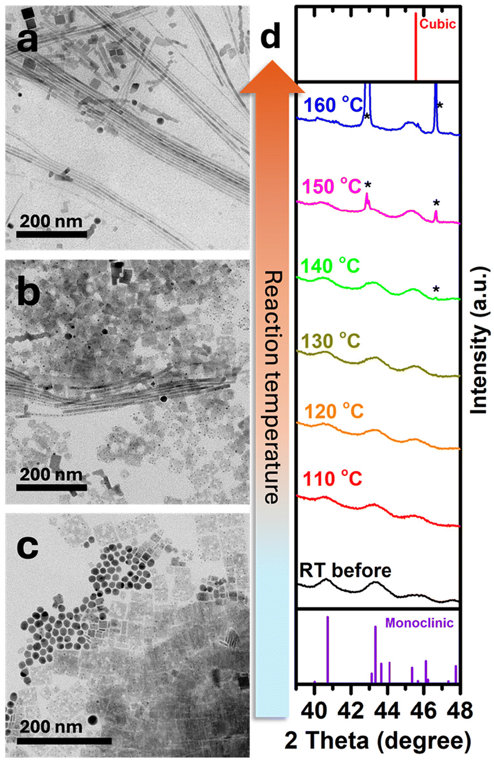 | ||
| Fig. 3 Ag2S activity as an SSS catalyst as a function of temperature. TEM image of Ag2S-catalyzed CsPbBr3 NWs (a) at 170 °C, (b) at 140 °C, and (c) at 120 °C. (d) In situ XRD patterns of Ag2S NPs in ODE as a function of temperature (in the 110–160 °C range); the asterisks (*) denote diffractions from the corundum crucible in which the measurement was monitored. | ||
For further investigation and study of the catalyst transition temperature effect, CsPbBr3 nanowires were synthesized at two temperatures (Fig. 3b and c): at 140 °C, we observed a mixture of rectangular nanoparticles and a minor nanowire product, while at 120 °C, only rectangular CsPbBr3 NPs and unreacted Ag2S nanoparticles were present. These results show that at 140 °C a partial phase transformation occurs; in contrast, at 120 °C Ag2S remains inactive since it is below the transformation temperature.
To investigate this transition in the reported system, we performed in situ XRD measurements29 of Ag2S NPs in ODE (similar conditions to the original synthesis). As shown in Fig. 3d at room temperature (black pattern; bottom), Ag2S NPs exhibit a monoclinic phase with dominant diffraction signals at 40.7° and 43.3° and a small peak at 45.5°. At 160 °C (blue pattern; top), a complete transformation into the superionic cubic phase occurs, with a single diffraction peak about 2θ = 45.5° attributed to the (211) plane (this position is close to the (112) plane of the monoclinic phase). The phase transition is evident from the changing ratio between the diffraction at 43.3° and 45.5°. At 130 °C (olive green pattern) and above, the experimental diffraction peak at ca. 45.5° becomes similar in intensity to the peak at 43.3°, indicating the partial transformation of some Ag2S NPs into the cubic phase. The overlap between the two phases increases the experimental intensity at 45.5° until it becomes the dominant peak after complete transformation at 160 °C.
Together with the TEM images (Fig. 3b and c) it confirms that CsPbBr3 NWs formation is temperature-dependent since the temperature determines Ag2S's phase, thus its catalytic activity, supporting the CsPbBr3 NWs growth mechanism being SSS.
One may expect that NWs synthesized via an SSS mechanism, like all catalyst-assisted growth nanowires, would have a catalyst decorating each tip. However, some NWs lack this feature (notably in the TEM images shown in Fig. 3). Yang and colleagues attributed this to the fragile nature of these materials and extensive purification, which can damage and break the NWs in their work on CsPbBr3 NWs preparation.13
We also noticed that the interface between the Ag2S catalyst and the CsPbBr3 NW is the weakest point, as shown in Fig. S6.† During image scanning, the HRSTEM image shows a separation between the two domains at the interface. This suggests that NWs without tips are either NW fragments or NWs that have lost their tip before imaging.
A kinetic study confirmed that each NW has a tip (a requirement for an SSS mechanism). In each separate synthesis, the reaction was quenched using a water bath at different times. The first synthesis was quenched immediately after the Cs-OA injection. As demonstrated in Fig. 4a, even after this brief reaction, CsPbBr3 NWs form, measuring around 100 ± 20 nm (Fig. S2†) in length.
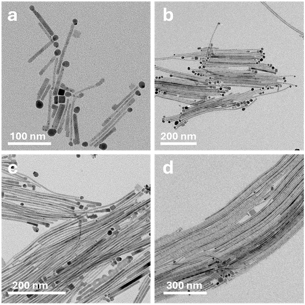 | ||
| Fig. 4 TEM images of Ag2S-catalyzed CsPbBr3 NWs reaction stages at different quenching times: (a) immediate quenching, (b) 5 s, (c) 1 min, and (d) 5 min. | ||
This length allows us to observe both ends of the NWs: each NW has the spherical Ag2S catalyst on the tip (dark contrast in the TEM image); some NWs have a cube at the other end, which will be discussed later. The short length of these NWs (Fig. 4a) can be explained by the relationship between the reaction temperature and the catalytic activity that we demonstrated in Fig. 3. The quenching process from 190 °C to the inactive 130 °C temperature takes 3–4 seconds, meaning even when reaction quenching is attempted, the catalyst remains active for about 3–4 s, which is sufficient for a 100 nm growth.
In Fig. 4b, where the synthesis was quenched 5 seconds later, the NWs grew to lengths of about 310 ± 90 nm (Fig. S2†). Most of them have a spherical tip supporting the SSS mechanism and a cube on the other side. Fig. S7† shows an HRSTEM image of five distinct NW tips from the same sample presented in Fig. 4b; two of them have the spherical Ag2S catalyst, and the others exhibit a cube-shaped tip that matches the same CsPbBr3 perovskite phase as the NW itself. The discussed CsPbBr3 cube is located opposite to the growth direction, leading us to believe that it forms at the beginning of the reaction. After the fast injection of Cs-OA, we propose that two processes occur concurrently: NW growth via an SSS mechanism and the typical CsPbBr3 nucleation and growth (‘regular’ growth mechanism). Most self-nucleated CsPbBr3 are washed out during the washing process, but the newly formed CsPbBr3 NW tip (via SSS) can also serve as a nucleus for a cube that would form on the older side of each NW by the end of the reaction. Therefore, as expected, the CsPbBr3 cubes also appear in the longer NWs (longer reaction times shown in Fig. 4c and d) and sometimes even on some NW fragments.
Rogach and co-workers noted that the perovskite CsPbBr3 crystallization process is very fast and takes 3–10 seconds to form cube-shaped NPs.36 This can explain why some of the short NWs in Fig. 4a do not have cubes on the tips.
During the described quenching process, the 3–10 seconds timeframe—which is required for the cube formation—is sufficient for cooling down the reaction medium to a temperature that prevents some of the cubes from crystallizing. However, these images explain the difference between the tips and show the temporal control over the NW length. Most importantly, they illustrate how fast this catalytic process occurs compared to other synthetic methods yielding CsPbBr3 NWs.
Thus far, we have demonstrated that Ag2S NPs can act as catalysts for forming CsPbBr3 NWs. However, this is not unique to Ag2S, as other materials with a superionic phase can also catalyze SSS growth. We first replaced Ag2S with Ag2Se, another known SSS catalyst. As seen in the TEM image (Fig. 5a), thin NWs with both spherical and cubical tips were formed, similar to those catalyzed by Ag2S. EDS mapping and spectra (Fig. S8 and S9†) confirm that the spherical Ag2Se catalyst is linked to the CsPbBr3 NW. Furthermore, the HRTEM image (Fig. 5b) shows that the darker contrast sphere corresponds to the orthorhombic Ag2Se phase, while the NW linked to these Ag2Se NPs is in the cubic perovskite CsPbBr3 phase. The UV–vis absorbance spectrum of the entire sample also shows the characteristic absorbance of CsPbBr3 perovskites with a local absorbance maximum at 493 nm and a PL emission at 516 nm (Fig. S10†).
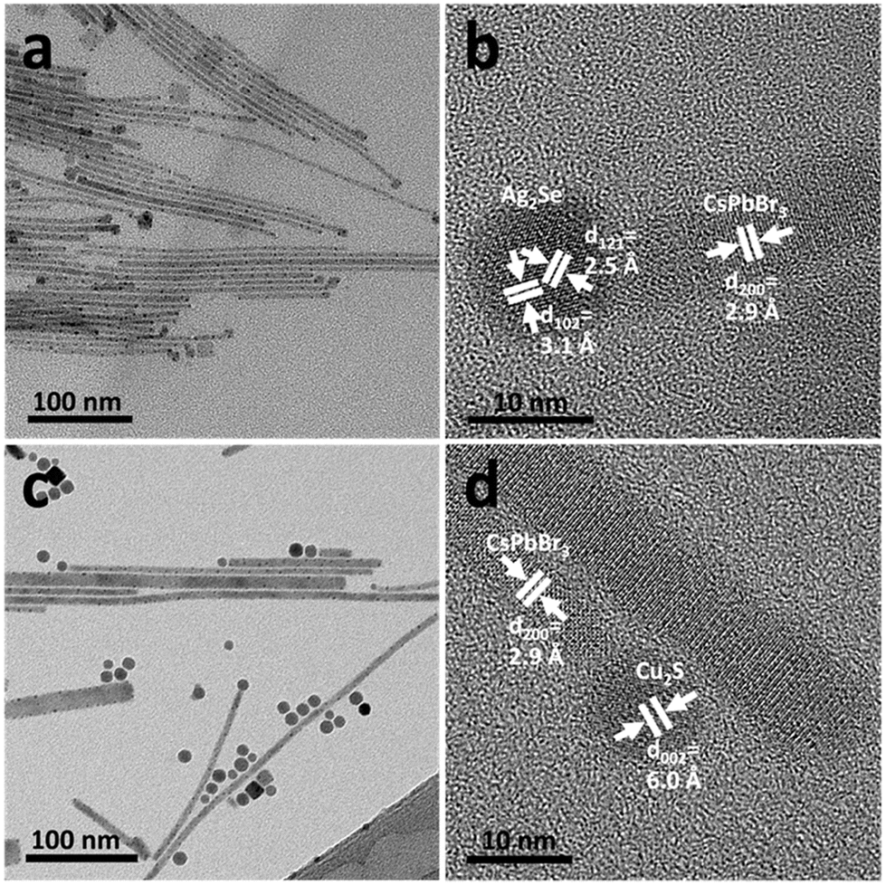 | ||
| Fig. 5 CsPbBr3 NWs synthesized with SSS catalysts. (a) TEM and (b) HRTEM images of Ag2Se-catalyzed NWs. (c) TEM and (d) HRTEM images of Cu2S-catalyzed NWs. | ||
Additionally, we have used Cu2S as the SSS catalyst. This experiment aimed to demonstrate the synthesis’ generality and show that the growth is not solely dependent on the presence of silver in the system. For the synthesis with Cu2S, we increased the reaction temperature to 220 °C to form the NWs (Fig. 5c), which is inconsistent with the simple relationship between the catalytic activity and temperature, as observed and described for the Ag2S system. The active superionic phase transition of Cu2S is Ttr, bulk = 105 °C;37 however, even at 190 °C, where the Cu2S is indeed in the active superionic phase, no NWs formed, suggesting that the phase transition is not the only factor affecting the reactivity of SSS catalysts.
The synthesis of the HP NWs using Cu2S catalyst has a lower yield compared to other two catalyst systems, possibly due to a combination of two reasons: (i) the relatively low reactivity of Cu2S, as observed in other works,19 and (ii) at higher temperatures, the self-nucleation process becomes more dominant, consuming the CsPbBr3 at the expense of the SSS process, which leads to lower NW yield. However, CsPbBr3 NWs form in the presence of a Cu2S catalyst, as shown in Fig. 5d; the darker contrast monoclinic Cu2S phase tip connects to a CsPbBr3 cubic perovskite phase NW, as expected from an SSS growth. The quantitative EDS spectra in Fig. S11† corroborate this analysis. To further prove the necessity of the superionic phase, we conducted a control experiment and replaced the catalyst with cubic CdS NPs (Fig. S12a†), keeping all other experimental conditions the same. As shown in Fig. S12b,† no NWs formed. This suggests that a requirement for a cubic phase or a chalcogenide material from a NP is not sufficient to allow CsPbBr3 NWs growth; an active superionic phase (such as Ag2S, Ag2Se, or Cu2S) is required for a successful catalyst-assisted SSS NW growth.
Conclusion
In conclusion, we have devised a novel approach to synthesize CsPbBr3 perovskite NWs using a catalyst-assisted growth mechanism. For the first time, we have synthesized CsPbBr3 perovskite NWs using superionic Ag2S NPs as a growth catalyst—a previously employed technique for 1D metal chalcogenides materials preparation. We have demonstrated the growth kinetics, highlighting the catalytic process’ speed. We have also illustrated how the phase transition of the catalyst at varying temperatures influences the final product and how versatile this method is by employing other known superionic SSS catalysts (specifically, Ag2Se and Cu2S). This technique paves a new way for forming HP NWs, demonstrating that these materials can be produced using catalyst-assisted growth methods such as solution–liquid–solid and vapor–liquid–solid.38,39 We envision that such catalyst-assisted growth methods would be beneficial for forming hybrid nanostructures that incorporate these HPs,24,34 or for fabricating arrays that can be integrated into devices.40Data availability
The data supporting this article have been included as part of the ESI. COD (XRD) card numbers, additional (S)TEM images and EDS, UV–vis and PL data.Conflicts of interest
There are no conflicts to declare.Acknowledgements
This work was supported by the Israeli Science Foundation (ISF, grant no. 1507/22). The authors thank Dr Vladimir Ezersky for helpful discussions and for high-resolution and analytical TEM. K. S. thanks the chemo-tech fellowship from the Kreitman School of Advanced Graduate Studies, Ben-Gurion University of the Negev, and the Council for Higher Education fellowship for outstanding doctoral students from the Arab community.References
- A. Kojima, K. Teshima, Y. Shirai and T. Miyasaka, J. Am. Chem. Soc., 2009, 131, 6050–6051 CrossRef CAS PubMed
.
- P. Li, X. Liu, Y. Zhang, C. Liang, G. Chen, F. Li, M. Su, G. Xing, X. Tao and Y. Song, Angew. Chem., Int. Ed., 2020, 59, 6909–6914 CrossRef CAS
- J. Xue, Z. Zhu, X. Xu, Y. Gu, S. Wang, L. Xu, Y. Zou, J. Song, H. Zeng and Q. Chen, Nano Lett., 2018, 18, 7628–7634 CrossRef CAS
- P. Docampo and T. Bein, Acc. Chem. Res., 2016, 49, 339–346 CrossRef CAS
- L. Wu, Y. Mu, X. Guo, W. Zhang, Z. Zhang, M. Zhang and T. Lu, Angew. Chem., Int. Ed., 2019, 58, 9491–9495 CrossRef CAS
- P. Chen, W. J. Ong, Z. Shi, X. Zhao and N. Li, Adv. Funct. Mater., 2020, 30, 1909667 CrossRef CAS
- M. V. Kovalenko, L. Protesescu and M. I. Bodnarchuk, Science, 2017, 358(6364), 745–750 CrossRef CAS
- Y. Tong, E. Bladt, M. F. Aygüler, A. Manzi, K. Z. Milowska, V. A. Hintermayr, P. Docampo, S. Bals, A. S. Urban, L. Polavarapu and J. Feldmann, Angew. Chem., Int. Ed., 2016, 55, 13887–13892 CrossRef CAS
- L. Protesescu, S. Yakunin, M. I. Bodnarchuk, F. Krieg, R. Caputo, C. H. Hendon, R. X. Yang, A. Walsh and M. V. Kovalenko, Nano Lett., 2015, 15, 3692–3696 CrossRef CAS
- H. Utzat, W. Sun, A. E. K. Kaplan, F. Krieg, M. Ginterseder, B. Spokoyny, N. D. Klein, K. E. Shulenberger, C. F. Perkinson, M. V. Kovalenko and M. G. Bawendi, Science, 2019, 363, 1068–1072 CrossRef CAS PubMed
- Y. Wang, X. Liu, Q. He, G. Chen, D. Xu, X. Chen, W. Zhao, J. Bao, X. Xu, J. Liu and X. Wang, Adv. Funct. Mater., 2021, 31, 202011251 Search PubMed
- D. Zhang, S. W. Eaton, Y. Yu, L. Dou and P. Yang, J. Am. Chem. Soc., 2015, 137, 9230–9233 CrossRef CAS
- D. Zhang, Y. Yu, Y. Bekenstein, A. B. Wong, A. P. Alivisatos and P. Yang, J. Am. Chem. Soc., 2016, 138, 13155–13158 CrossRef CAS PubMed
- M. Imran, F. Di Stasio, Z. Dang, C. Canale, A. H. Khan, J. Shamsi, R. Brescia, M. Prato and L. Manna, Chem. Mater., 2016, 28, 6450–6454 CrossRef CAS
- Y. Liu, M. Guo, S. Dong, X. Jiao, T. Wang and D. Chen, J. Mater. Chem. C, 2018, 6, 7797–7802 RSC
- Y. Tong, B. J. Bohn, E. Bladt, K. Wang, P. Müller-Buschbaum, S. Bals, A. S. Urban, L. Polavarapu and J. Feldmann, Angew. Chem., Int. Ed., 2017, 56, 13887–13892 CrossRef CAS PubMed
- J. Liu, K. Song, Y. Shin, X. Liu, J. Chen, K. X. Yao, J. Pan, C. Yang, J. Yin, L.-J. Xu, H. Yang, A. M. El-Zohry, B. Xin, S. Mitra, M. N. Hedhili, I. S. Roqan, O. F. Mohammed, Y. Han and O. M. Bakr, Chem. Mater., 2019, 31, 6642–6649 CrossRef CAS
- L. He, S. Pan, Z. Lin and J. Peng, ACS Appl. Nano Mater., 2019, 2, 7910–7915 CrossRef CAS
- J. Wang, K. Chen, M. Gong, B. Xu and Q. Yang, Nano Lett., 2013, 13, 3996–4000 CrossRef CAS
- Q. Li, C. Zou, L. Zhai, L. Zhang, Y. Yang, X. Chen and S. Huang, CrystEngComm, 2013, 15, 1806 RSC
- Y. Li, Z.-C. Shao, C. Zhang and S.-H. Yu, J. Phys. Chem. Lett., 2021, 12, 10695–10705 CrossRef CAS
- F. Wang, A. Dong and W. E. Buhro, Chem. Rev., 2016, 116, 10888–10933 CrossRef CAS
- Y. Sun, T. Dong, L. Yu, J. Xu and K. Chen, Adv. Mater., 2019, 32, 1903945 CrossRef
- K. Shreteh, M. Volokh, V. Ezersky and T. Mokari, Chem. Mater., 2021, 33, 4701–4708 CrossRef CAS
- N. Afik, K. Shreteh, H. Fridman, M. Volokh, V. Ezersky and T. Mokari, Chem. Mater., 2021, 33, 9326–9333 CrossRef CAS
- K. Shreteh, S. Murugesan, I. Alkrenawi, N. Afik, M. Volokh and T. Mokari, Inorg. Chem., 2024, 63, 431–440 CrossRef CAS
- D. Wang, T. Xie, Q. Peng and Y. Li, J. Am. Chem. Soc., 2008, 130, 4016–4022 CrossRef CAS PubMed
- Z. Zhuang, X. Lu, Q. Peng and Y. Li, Chem. – Eur. J., 2011, 17, 10445–10452 CrossRef CAS
- H. Fridman, M. Volokh and T. Mokari, Nanoscale, 2021, 13, 19076–19084 RSC
- S. Hoshino, Solid State Ionics, 1991, 48, 179–201 CrossRef CAS
- F. Wang and W. E. Buhro, ACS Nano, 2017, 11, 12526–12535 CrossRef CAS PubMed
- T. Zhuang, P. Yu, F. Fan, L. Wu, X. Liu and S. Yu, Small, 2014, 10, 1394–1402 CrossRef CAS PubMed
- W. Han, L. Yi, N. Zhao, A. Tang, M. Gao and Z. Tang, J. Am. Chem. Soc., 2008, 130, 13152–13161 CrossRef CAS PubMed
- Y. Li, C. Zhang, T.-T. Zhuang, Y. Lin, J. Tian, X.-Y. Qi, X. Li, R. Wang, L. Wu, G.-Q. Liu, T. Ma, Z. He, H.-B. Sun, F. Fan, H. Zhu and S.-H. Yu, J. Am. Chem. Soc., 2021, 143, 7013–7020 CrossRef CAS
- J. Liu, L. Chen, H. Yang, Z. Zhang and Y. Wang, Prog. Nat. Sci.: Mater. Int., 2019, 29, 397–401 CrossRef CAS
- K. Vighnesh, S. Wang, H. Liu and A. L. Rogach, ACS Nano, 2022, 16, 19618–19625 CrossRef CAS
- L.-W. Wang, Phys. Rev. Lett., 2012, 108, 085703 CrossRef PubMed
- T. J. Trentler, K. M. Hickman, S. C. Goel, A. M. Viano, P. C. Gibbons and W. E. Buhro, Science, 1995, 270, 1791–1794 CrossRef CAS
- Q. Gao, V. G. Dubrovskii, P. Caroff, J. Wong-Leung, L. Li, Y. Guo, L. Fu, H. H. Tan and C. Jagadish, Nano Lett., 2016, 16, 4361–4367 CrossRef CAS PubMed
- E. Oksenberg, E. Sanders, R. Popovitz-Biro, L. Houben and E. Joselevich, Nano Lett., 2018, 18, 424–433 CrossRef CAS
Footnote |
| † Electronic supplementary information (ESI) available: COD (XRD) card numbers, additional (S)TEM images and EDS, UV–vis and PL data. See DOI: https://doi.org/10.1039/d4nr03158j |
| This journal is © The Royal Society of Chemistry 2025 |