
Colloidal semiconductor quantum shells for solution-processed laser applications
Divesh
Nazar
,
Amelia Dawn
Waters
,
Maxwell Marshal
Kannen
,
Dulanjan
Harankahage
,
Jiamin
Huang
and
Mikhail
Zamkov
 *
*
The Canter for Photochemical Sciences and Department of Physics, Bowling Green State University, Bowling Green, Ohio 43403, USA. E-mail: zamkovm@bgsu.edu
First published on 7th January 2025
Abstract
Laser diodes based on solution-processed semiconductor quantum dots (QDs) present an economical and color-tunable alternative to traditional epitaxial lasers. However, their efficiency is significantly limited by non-radiative Auger recombination, a process that increases lasing thresholds and diminishes device longevity through excessive heat generation. Recent advancements indicate that these limitations can be mitigated by employing spherical quantum wells, or quantum shells (QSs), in place of conventional QDs. The unique QS geometry is designed to suppress multi-exciton Auger decay through exciton–exciton repulsion, thereby extending multi-exciton lifetimes and enhancing their radiative recombination efficiency. In this review, we examine optoelectronic characteristics of QSs and discuss their integration into photonic laser cavities. We further present experimental data demonstrating QS performance in femtosecond, quasi-continuous-wave (quasi-CW), and two-photon upconverted laser configurations, underscoring QS capability to achieve efficient lasing with reduced thresholds and lower energy losses.
Divesh Nazar obtained his BS-MS degree from Indian Institute of Science Education and Research Thiruvananthapuram, India. He is currently pursuing his PhD at Center for Photochemical Sciences, Bowling Green State University under the supervision of Dr Mikhail Zamkov. |
Amelia Waters obtained her bachelor's degree from Bowling Green State University. She is currently pursuing her PhD in Photochemistry at Bowling Green State University working under the supervision of Dr Mikhail Zamkov. |
Maxwell Kannen is a senior college student at Bowling Green State University where he's pursuing a double major in Applied Mathematics and Physics at Bowling Green State University. He's an undergraduate research assistant working on synthesizing/characterizing colloidal semiconductor nanomaterials at Zamkov lab. |
Dulanjan Harankahage earned his bachelor's degree from University of Sri Jayewardenepura, Sri Lanka. Afterwards he pursued master's degree at the department of Physics and Astronomy, Bowling Green State University and went on to continue his Ph.D. work in the photochemical sciences center at Bowling Green State University working under the supervision of Dr Mikhail Zamkov. |
Jiaming Huang obtained her B.Sc. in Jiaying University, China in 2011 and continued her MSc at Jinan University where she graduated in 2015. She's currently pursuing her PhD colloidal semiconductor nanomaterials at photochemical sciences center, Bowling Green State University. |
Prof. Mikhail Zamkov obtained his Ph.D. degrees from Kansas State University in 2003. He is now a Full Professor at Bowling Green State University. His research focuses on the electronic, chemical, and optical properties of semiconductor nanostructures and hybrid nanoscale materials prepared by means of colloidal synthesis. (https://physics.bgsu.edu/~zamkovm/). |
Introduction
The development of lasers compatible with silicon-based semiconductor systems remains a major challenge in optoelectronics.1–3 Current methods, such as wafer-bonding or the incorporation of epitaxial III–V quantum dot (QD) lasers, are not only technically complex but also expensive, which limits their scalability and widespread usage.4 A promising alternative is solution-processed materials, which offer a more affordable pathway for integrating both photonic and electronic components into silicon-based systems.5 By reducing production costs and improving scalability, this technology has the potential to accelerate advancements in photonic circuits, telecommunications, quantum computing, medical diagnostics, and wearable devices.6Colloidal semiconductor nanocrystals (NCs)7,8 show strong promise as candidates for the development of solution-processed lasers,9,10 combining the durability of traditional semiconductors with the electronic properties of molecular systems. Their emission can be continuously tuned across a wide spectral range, from ultraviolet to infrared, by selecting an appropriate nanoparticle size and composition.7,11 Compared to bulk semiconductors, NCs also offer the benefits of low optical-gain thresholds and high temperature stability of lasing characteristics.5 However, the employment of colloidal NCs in lasers is hindered by Auger recombination, a process where multiple charge carriers transfer energy non-radiatively, affecting optically active carriers like biexcitons (XX) and multiexcitons (MX).9,12,13 This issue greatly reduces the efficiency of lasing applications and shortens the device lifespan due to heat generation.
Significant progress in mitigating Auger recombination has been achieved through the development of advanced NC architectures, such as composition-graded QDs and nanoplatelets (NPLs). Graded QDs,14,15 known for their long biexciton lifetimes, have been successfully utilized in continuous-wave lasing16 and electrically pumped gain media.17–19 Meanwhile, in NPLs, the band-edge gain was shown to reach near-record values, attributed to stimulated emission from a degenerate e–h plasma.19–21 Despite these promising characteristics, the optical gain achieved in these structures remains suboptimal. Graded QDs, for example, exhibit relatively low biexciton photoluminescence quantum yields (PL QY), often below 40%, which not only limits optical gain but also increases heat generation within QD films. NPLs, despite having an over 90% biexciton PL QY in certain cases, have shorter XX emission lifetimes,22 which pose challenges for optical gain development and their ability to achieve low lasing thresholds in optical microcavity configurations.
Recent studies have introduced a novel, spherical-shell NC geometry, designed to address the challenges associated with short MX lifetimes of colloidal NCs. These so-called quantum shells (QSs) represent a spherical quantum well structure comprising a narrow-gap, quantum-confined spherical shell (e.g. CdSe) sandwiched between wider-gap, bulk-size core and outer shell components (e.g. CdS), forming a spherical quantum well structure (see Fig. 1a, d and e).23–34 Similar to nanoplatelets, QSs provide carrier confinement in only one dimension but with repulsive rather than attractive interactions between multiple excitons. The exciton repulsion minimizes carrier overlap, significantly reducing Auger recombination rates. As a result, the radiative emission from biexcitons in QSs can approach nearly 100%,29 representing a major advancement for the development of high-efficiency optical devices (see Fig. 1b and c). This review will explore the multi-exciton properties of colloidal QSs, with an emphasis on recent advancements in the development of solution-processed quantum shell lasers.
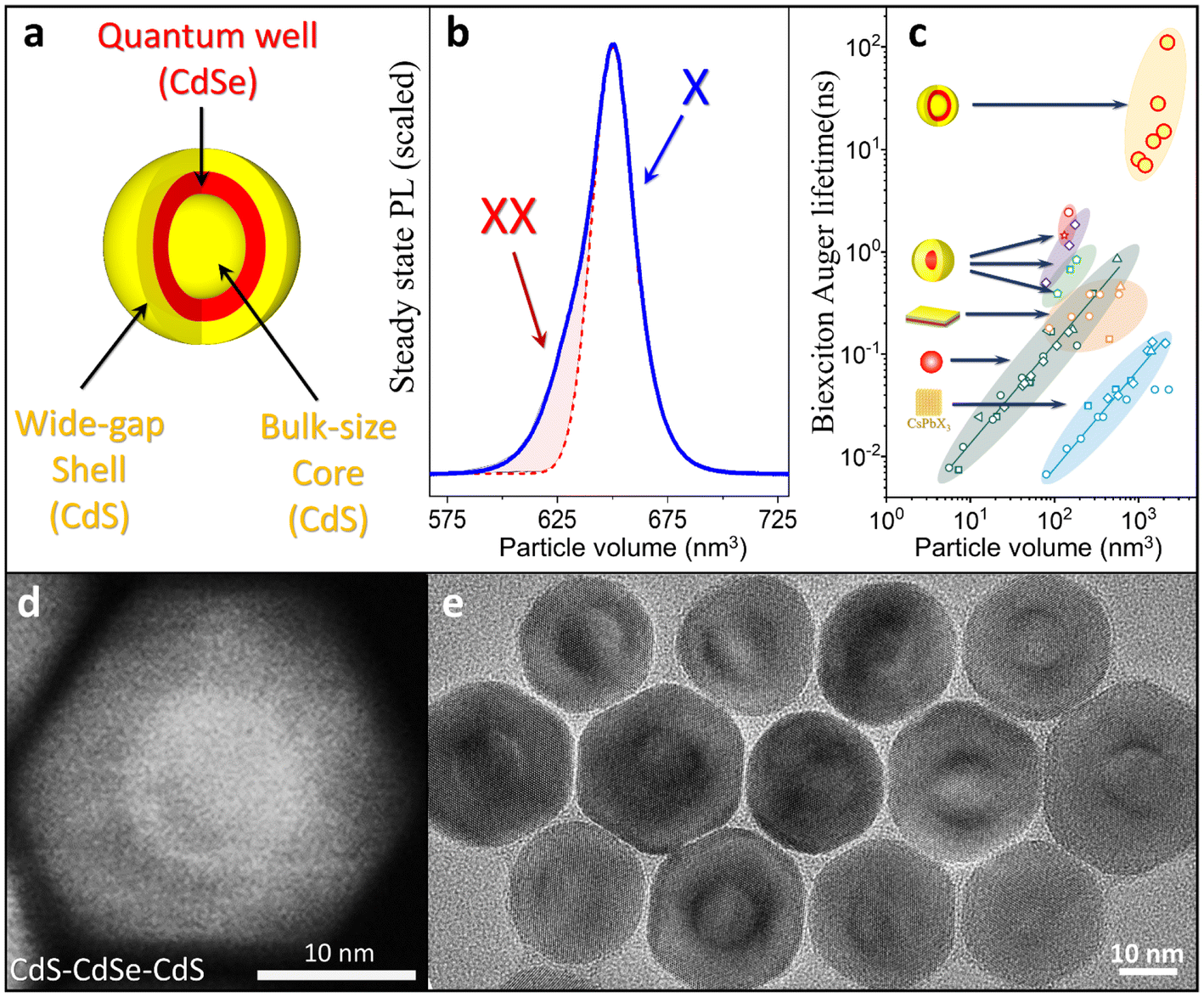 | ||
| Fig. 1 (a) The schematic geometry of a CdSbulk–CdSe–CdS QS. (b) Steady-state PL of CdS–CdSe–CdS QSs showing the contribution from biexciton emission on the high energy side of single-exciton PL peak. (c) The dependence of biexciton Auger lifetimes on particle volume for different types of colloidal NCs. (d) Characteristic high angle annular dark field (HAADF)-STEM image of a CdS–CdSe–CdS QS, illustrating the location of the CdSe shell layer. (e) Characteristic TEM image of 14 nm-core CdS–CdSe–CdS QSs. Adapted with permission from ref. 34. Copyright 2023 The Royal Society of Chemistry. Panel c adapted with permission from ref. 42. Copyright 2021. Springer Nature. | ||
Geometry of QSs
The QS geometry is based on a spherical quantum well structure confined between a core and an outer shell of a wider bandgap semiconductor. While this design shares similarities with Quantum-Dot Quantum Wells (QDQWs),35–41 it is distinguished by a relatively large diameter of its core. This feature allows QSs to maintain quantum confinement within a significantly larger nanostructure volume compared to other NC morphologies. For instance, in 14 nm-core CdS–CdSe–CdS QSs shown in Fig. 1e, the CdSe spherical layer has a diameter of approximately 17 nm. Remarkably, despite such a large size, these structures exhibit apparent quantum confinement characteristics, including spectrally tunable photoluminescence.A larger-volume core of a QS structure provides greater space for multiple excitons, effectively reducing coulombic interactions between charge carriers and significantly decreasing Auger recombination rates. Additionally, the increased total size of QSs results in a reduced surface-to-volume ratio, which in turn decreases the rate of carrier surface recombination. Consequently, the two key features of a QS geometry—enhanced exciton volume and reduced surface-to-volume ratio—work in tandem to suppress non-radiative decay processes in semiconductor colloids, namely Auger recombination and surface recombination. This makes QSs particularly beneficial for optoelectronic applications requiring exciton stability and long multi-exciton lifetimes.
Synthesis and optical properties of CdS–CdSe–CdS QSs
The synthesis of CdSe-based QSs employs growing each QS layer in separate reactions, allowing for solvent optimization tailored to specific precursor combinations. The process begins with the synthesis of large CdS core nanoparticles (5–20 nm in diameter) using an aggregative growth method, which promotes particle size focusing via coalescence.43 During this process, small nanocrystals collide and fuse due to the high surface free energy of smaller particles, leading to stable, equilibrium shapes and morphologies, as was independently observed by several groups.43–45 The proposed model explained such a fusion process as due to the formation of a eutectic mixture between CdS and CdCl2 phases,46,47 which lowers the melting point below that of the pure components, resulting in a molten phase. Evidence supporting this mechanism includes in situ observations of particle fusion during synthesis (ref. 49) and post-synthesis analysis of narrow size distributions48 that cannot be explained by conventional growth models. This thermodynamically-driven synthesis is particularly efficient for the growth of large NCs, where the nanoparticle size is determined by the growth temperature, independent of the initial size or morphology of seeding NCs. In the second step, a CdSe layer is deposited over the CdS core using a solvent mixture of octadecene and amines. The final step involves capping the CdSe shell with either a thick CdS shell or a partly alloyed CdS/ZnS composite shell. QSs capped with CdS/ZnS exhibit higher PL QY, often exceeding 90%, while those with CdS-only shells exhibit PL QYs ranging from 50% to 90%, depending on the shell thickness. Controlled shell growth at any stage of the reaction is achieved via slow precursor injection using syringe pumps, ensuring reproducible synthesis.Fig. 2 illustrates the overall growth scheme (a) and corresponding optical spectra (b–d) for the three stages of QS formation. This example highlights a medium-core structure with a CdS–CdSe–CdZnS core–shell–shell configuration, featuring a 7.2 nm CdS core. The initial coalescence of 2–3 nm CdS seeds is achieved in an oleylamine/CdCl2 mixture at temperatures above 220 °C, with the final 7.2 nm core size reached at 240 °C. The emission spectrum of the CdS core (Fig. 2b) displays a narrow linewidth, indicating a uniform size distribution, as further corroborated by the TEM image in Fig. 2e. The subsequent deposition of the CdSe shell is accompanied by the onset of PL, tunable across the 600–695 nm range (Fig. 2c). The TEM image in Fig. 2f reveals a 3.5 nm increase in particle size relative to the initial CdS NCs. In the final stage, the addition of a CdS or CdS/ZnS graded shell induces thermodynamic reshaping of the nanoparticles into hexagonal prisms (Fig. 2g). This restructuring improves QS optical properties, including a reduced emission linewidth (Fig. 2d) and an enhanced PL QY. We speculate that the structural changes during the final shell deposition are facilitated by high-temperature growth conditions (>310 °C) and the use of thiols as sulphur precursors. Similar to CdCl2, thiols act as “fluxing” agents, forming a eutectic mixture that promotes lattice reorganization and contributes to the superior optical properties of the colloidal semiconductors.49
 | ||
| Fig. 2 (a) Schematic representation of the CdS–CdSe–CdS–ZnS QS synthesis, illustrating the key steps including the CdS core growth via coalescence and the subsequent deposition of shell layers. (b–d) Absorption and emission spectra of NCs during different phases of the synthesis, showing spectral evolution from the bulk 7.2 nm CdS core – (b) to the intermediate CdS/CdSe structure – (c), and the final CdS–CdSe–CdS–ZnS QS configuration – (d), (e–g) TEM images corresponding to the same stages of the synthesis as in panels b–d, depicting the morphological changes from the initial core formation through to the fully grown QS structure. Panels (d, g) adapted with permission from ref. 28. Copyright 2023 American Chemical Society. | ||
Emission characteristics of multi-exciton states
To quantify the contribution of Auger recombination processes into the multi-exciton decay of QSs, we have measured the quantum yield of biexciton emission, QYXX. To this end, we recorded the second-order cross-correlation function, g(2)(τ), which quantifies the ratio of the peak at zero-time delay (τ = 0) to the side peaks.50 The resulting value is therefore equal to the probability of detecting two photons simultaneously during one excitation cycle. To determine g(2)(τ) experimentally, we have used fluorescence correlation spectroscopy,51 which employs a Hanbury–Brown–Twiss setup consisting of a confocal microscope and a pulsed excitation source. By collecting emissions from a large number of diffusing nanoparticles, this method provides an ensemble-average value for QYXX, enabling a reliable estimate of the Auger recombination rate.The results of the fluorescence correlation spectroscopy measurements are summarized in Fig. 3b and c. the QYXX/QYX quantum yield ratios were determined to be 57% in a medium-core (7.2 nm) and 79% in a large-core (8.7 nm) QSs.28 We note that biexciton quantum yields in zero-dimensional CdSe/CdS core/shell QDs are typically lower, with QYXX/QYX values ranging from 10% to 40%.52,53 The corresponding Auger lifetimes of XX states in QSs were then estimated to be 22 ns for the 7.2 nm core and 90 ns for the 8.7 nm core QSs, assuming quadruple scaling of the biexciton radiative rate relative to that of single excitons.28 Notably, larger-core QSs consistently exhibited higher biexciton quantum yields and longer Auger lifetimes compared to their smaller-core counterparts. It was concluded that the increased exciton volume in larger core samples was the key factor contributing to the reduced probability of non-radiative Auger recombination (see Fig. 3f).
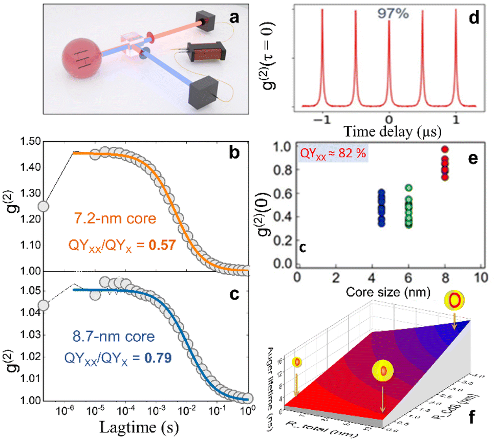 | ||
| Fig. 3 (a) Schematics of radiative XX–X cascade, second-order cross-correlation measurements. (b and c) Lagtime-dependence of the cross-correlation function, g(2) that was used to determine the ratio of biexciton to exciton QY (QYXX/QYX) for (c) – 7.2 nm core QSs and (d) – 8.7 nm core QSs. The displayed cross-correlation function represents the integrated intensity of the correlation peak, as detailed in ref. 51. (d) An example of g(2)(τ) functions for 8.0 nm core CdS/CdSe/CdS QSs. (e) Statistics of g2(τ) values for 8.0 nm core CdS/CdSe/CdS QSs. (f) Calculated Auger times as a function of overall and CdS core sizes. Panel (b, c) adapted with permission from ref. 28. Copyright 2023 American Chemical Society. Panel (d–f) adapted with permission from ref. 29. Copyright 2023 American Chemical Society. | ||
Single-particle measurements of g(2), such as those reported by A. Malko and colleagues,29 have demonstrated even higher biexciton quantum yields, with values averaging at 82% (see Fig. 3e) and individual particles achieving nearly 100% QYXX (Fig. 3d). Meanwhile, a variable-power rate scaling model, which calculates time-dependent PL intensities as a function of the average number of excitons per QS, has reported biexciton Auger lifetimes of 50 ns for 7.2 nm cores and up to 110 ns for 8.7 nm cores.28 These findings highlight the potential for further optimization of QS geometries, particularly as Auger suppression improves with increasing core size.
Unusually long Auger lifetimes in QSs provide significant benefits for advancing the practical use of colloidal semiconductors in optoelectronic applications. These are particularly beneficial in lasing systems, where Auger recombination is a primary limiting factor for achieving efficient light amplification. Suppressing Auger decay also enhances the biexciton–exciton radiative cascade, a process essential for improving the performance of high-brightness light-emitting diodes (LEDs),54–56 ionizing radiation scintillators,57,58 and other technologies that rely on multi-exciton dynamics.59 Additionally, longer Auger lifetimes reduce heat generation within nanocrystals, thus significantly improving the thermal management, operational stability, and reliability of devices exposed to high levels of electrical or optical excitation. This combination of enhanced efficiency and reduced thermal degradation, positions QSs as promising materials for the next generation optoelectronic devices.
Optical gain in colloidal QSs
The suppression of Auger recombination in QSs enables efficient light amplification across both XX and MX gain regimes. Notably, QSs also support a single-exciton optical gain mode, effectively neutralizing the Auger recombination.25 This single-exciton gain is facilitated by the splitting of X and XX energy levels, induced by the photoinduced electric field of a spatially separated electron–hole pair.60,61 Single-particle measurements of QSs at 10 K reveal a large exciton–biexciton energy separation (Fig. 4a). Previously, such X–XX energy splitting, exceeding room temperature kT, was observed only in type II heterostructured nanocrystals, where the electron–hole overlap is minimal.62 However, QSs exhibit this energy splitting despite being a type I system, with a substantial exciton–biexciton energy (ΔXX) ranging from 57 to 80 meV.34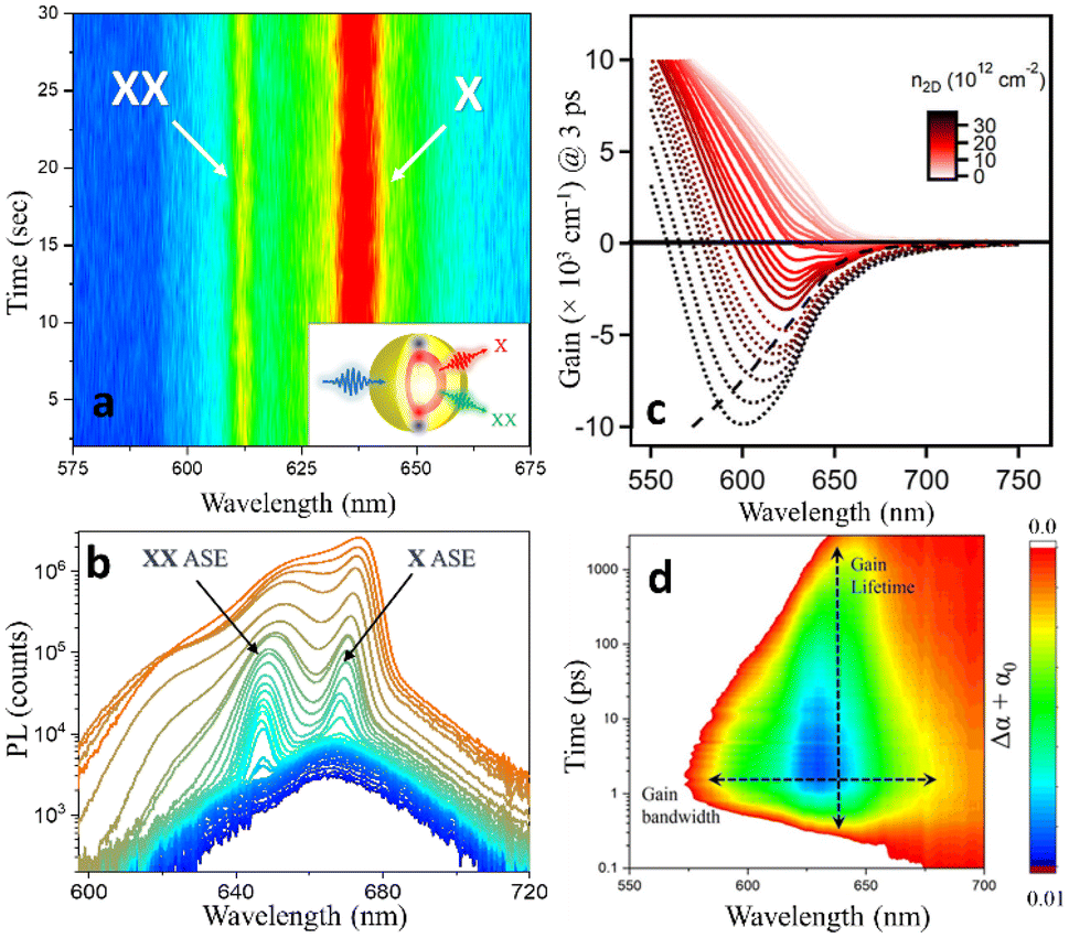 | ||
| Fig. 4 (a) Single quantum shell spectra recorded at 10 K over a 30-second period, illustrating the spectral separation between biexciton (XX) and exciton (X) emission lines. (b) Emission spectra observed from thin films of 7.2 nm-core QSs for different pump fluences. The narrow ASE peak at ∼650 nm corresponds to biexciton optical gain, while the onset of a lower-energy feature at around 670 nm, matching the spectral position of the photoluminescence peak, is attributed to a single-exciton gain mechanism. (c) Intrinsic absorption at a 3 ps time delay, demonstrating net gain (negative values) emerging from an average of approximately 3 electron–hole pairs per QS stretches from 560 to 700 nm for the highest densities used. (d) Contour plot showing the lifetime and bandwidth of optical gain in 4.5 nm-core QSs. Positive gain is achieved when the sum – (α + Δα) is greater than zero. The pump fluence for this case is 36 μJ cm−2. Panel b adapted with permission from ref. 28. Copyright 2023 American Chemical Society. Panel c adapted with permission from ref. 31. Copyright 2024 American Chemical Society. Panel d adapted with permission from ref. 25. Copyright 2022 American Chemical Society. | ||
The amplified spontaneous emission (ASE) spectra of 7.2 nm-core CdS–CdSe–CdS–ZnS QSs, shown in Fig. 4b, clearly demonstrate X–XX energy splitting. Based on the power-dependent behaviour of these features (see ref. 29), the higher-energy ASE peak was attributed to the XX state, indicating exciton–exciton repulsion within the QS. The single-exciton ASE is detected as a sharp peak on top of the broader PL band. The energy difference between the exciton and biexciton ASE features in this case was 63 meV. Importantly, biexciton ASE was observed at a low pump fluence of 5.3 μJ cm−2, highlighting the high optical gain efficiency of the QS system.
The amplified stimulated emission properties of QSs were explored through femtosecond transient absorption (TA) measurements.25 These measurements tracked absorption changes (Δα) induced by a femtosecond pump pulse, revealing a gain regime where Δα + α < 0 (see Fig. 4d). A contribution from a single-exciton gain enabled a long optical gain lifetime τgain > 6 ns, among the longest reported for colloidal NCs. Meanwhile, the suppression of non-radiative Auger decay processes allowed for optical gain across a broad spectral bandwidth (∼300 meV). This broad gain window is not typically observed in conventional core–shell QDs due to shorter MX lifetimes. We note that such a combination of a long gain lifetime and broad spectral amplification range make QSs particularly promising for in light amplification applications.
In a related study,31 optical gain in CdS–CdSe–CdS–ZnS QSs was examined using a 170 fs pump pulse at 515 nm (2.4 eV). The results revealed that at high excitation densities, the gain window extended from 550 to 680 nm without any signs of saturation (Fig. 4c). At extreme carrier densities above 1013 cm−2, the observed spectral shifts were attributed to strong band gap renormalization, a phenomenon commonly seen in both bulk and 2D semiconductors.63 A kinetic trace near the band gap at 650 nm indicated a long optical gain lifetime (τgain) of up to 6 ns. Additionally, PL spectra collected following photoexcitation exhibited features that matched those seen in the optical gain, reinforcing the consistency of these observations.
Lasing applications of colloidal QSs
Lasing applications of colloidal QSs are still in the early development stages but have already shown promising results. Recent studies have demonstrated quantum shells as a low-loss, broadband gain media in optically pumped laser cavities. These advancements include femtosecond and quasi-continuous wave (quasi-CW) lasing, which take advantage of the Auger suppression inherent in QS structures. Additionally, the upconverted lasing through two-photon excitation has been successfully achieved, opening new avenues for efficient nonlinear optical devices. The following sections provide a detailed discussion of these demonstrations.Lasing from colloidal QSs in optical nanocavities
A recent work by Malko and co-workers29 demonstrated lasing from QSs deposited onto nanopillar arrays on silicon substrates (Fig. 5a and b). Lasing was achieved with a notably low threshold pump fluence of approximately 4 μJ cm−2 (Fig. 5f), which stands as one of the lowest recorded values for colloidal NCs in photonic crystal cavities.64 One of the key advantages of using QSs for light amplification is their ability to support a wide range of emission wavelengths from a single material system. In this study, lasing was observed across a broad spectral range (see Fig. 5c–e), covering single exciton (λX ≈ 640 nm), biexciton (λXX ≈ 625 nm), and multiexciton (λMX ≈ 615–565 nm) transitions. Spectral tuning was achieved by adjusting the array period of the nanopillars while maintaining high-quality (Q) factors and mode confinement within the cavity, as demonstrated in Fig. 5g and j. Importantly, the experimental lasing emission spectrum closely aligned with theoretical model predictions, validating the design of the system.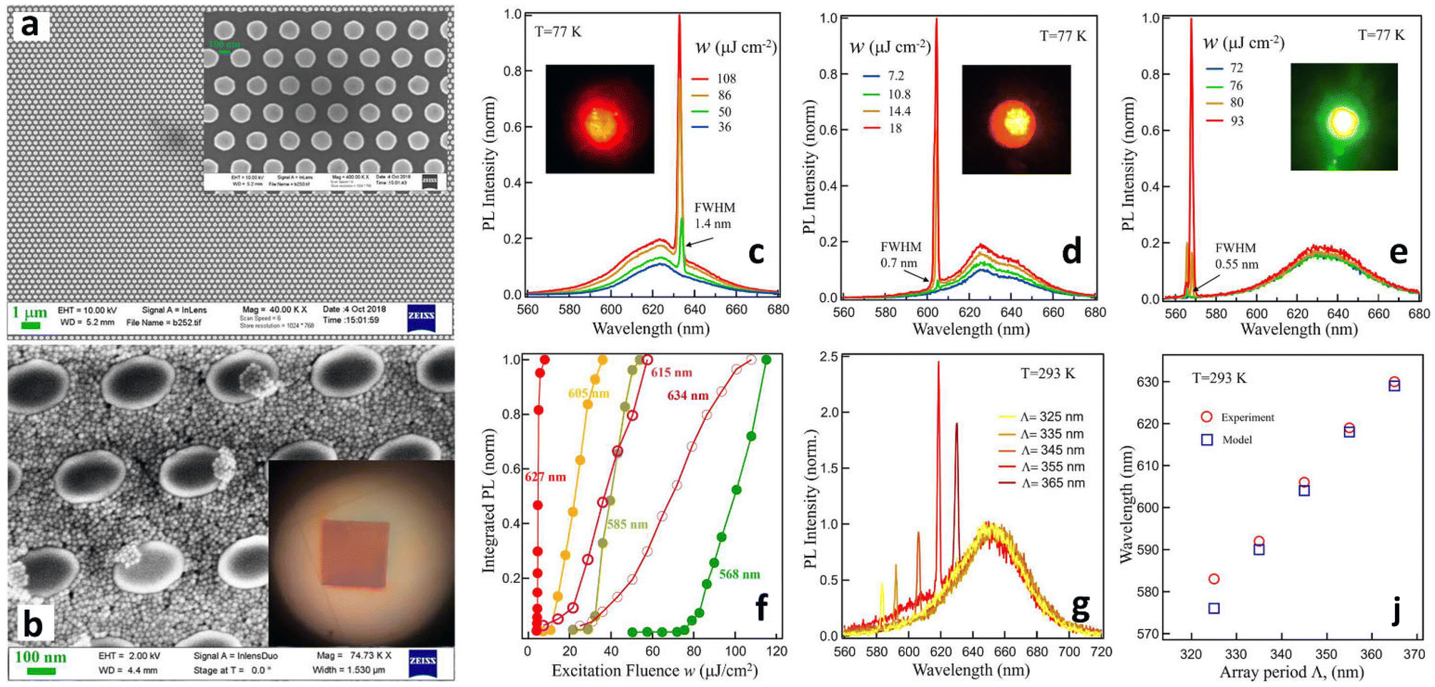 | ||
| Fig. 5 (a) Scanning Electron Microscope (SEM) image of the photonic crystal nanopillar array with a period of Λ = 335 nm. Scale bar = 1 μm. Inset: Zoomed-in view of the array. Scale bar = 100 nm. (b) SEM image of the nanopillar array after spin-coating with QS. Inset: Optical image showing the entire nanopillar array post spincoating. (c–e) Lasing emission spectra measured at T = 77 K for different array periods: (c) Λ = 365 nm, (d) Λ = 335 nm, and (e) Λ = 315 nm. Insets: Microphotographs of lasing spots. (f) Lasing thresholds plotted as a function of excitation fluence for the various lasing lines. (g) Lasing emission spectra at T = 293 K. (h) Comparison of calculated (blue) versus experimental (red) positions of the lowest energy resonance (lasing) peaks as a function of the nanopillar array periods at T = 293 K. Adapted with permission from ref. 30. Copyright 2024 American Chemical Society. | ||
The ensemble-averaged gain threshold for these devices was around 1.4 electron–hole pairs per QS, closely matching the theoretical minimum for achieving the amplified emission in these materials.27 This demonstrates the importance of Auger suppression on the efficiency of the lasing processes. By reducing non-radiative recombination pathways, the QS system leads to an efficient light amplification at a relatively low pump threshold, comparable to the best-performing colloidal nanocrystals used in distributed feedback (DFB) configurations.65,66
Quasi-CW lasing from colloidal QSs in photonic crystals
Another demonstration of QS lasing was detailed in a recent study,31 where QSs were employed to fabricate photonic crystal surface-emitting lasers (PCSELs) using a silicon nitride (SiNx-on-SiOx) photonic platform.67 This design incorporated a square lattice two-dimensional photonic crystal cavity, where periodic etching in a 170 nm thick SiNx layer created the photonic structure (see Fig. 6a). The lattice periods, ranging from 320 to 460 nm, were designed based on Bragg's Law (m·λBragg = 2neffΛ), with a second-order grating used to achieve surface emission. The cavities were subsequently coated with a layer of QSs via spin-coating, forming QS-PCSEL devices. Cross-sectional SEM imaging confirmed a 70% duty cycle and full infilling of the etched cavities (see Fig. 6a and b).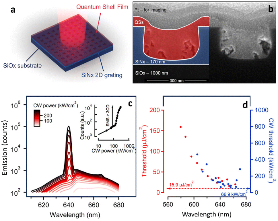 | ||
| Fig. 6 (a) Schematic of the device and (b) cross-sectional SEM image, highlighting the quantum shell layer in red and the silicon nitride (SiNx) photonic crystal surface layer in blue. (c) Emission spectra under quasi-CW excitation using 7 ns pulses at 532 nm. The inset displays the increase in peak intensity with increasing pump flux. (d) Thresholds for femtosecond (red) and quasi-CW (blue) excitation, showing a clear correlation and a minimum within the 640–660 nm spectral window. Adapted with permission from ref. 31. Copyright 2024 American Chemical Society. | ||
Optical pumping was carried out using a 100 Hz, 7 ns pulsed laser at 532 nm. The pulse duration, matching the longest QS gain lifetime (∼6 ns), allowed for a quasi-CW regime, where electron–hole pairs were created and annihilated multiple times per pulse. Quasi-CW lasing emission, observed across the 600–670 nm range, achieved a low threshold of 66.9 kW cm−2 at 660 nm, corresponding to multiple electron–hole pairs per QS. The quasi-CW lasing exhibited remarkable stability, showing no performance degradation even after one million laser excitation cycles. Such an impressive stability was attributed to the radiative recombination of the “plasma” state, giving more photons back at a high pump rate instead of heating the device through Auger processes. Notably, there is only one previous report of CW lasing in colloidal NCs.68 In that study, Klimov, Sargent, and colleagues achieved CW lasing by utilizing biaxially strained QDs resulting in a lasing threshold of approximately 7 kW cm−2. Overall, the observation of quasi-CW lasing in QSs underscores their potential for low-threshold, high-stability lasing applications, particularly using PCSELs as an efficient platform for future optoelectronic devices.
Two-photon “upconverted” lasing from colloidal QSs
Recent studies have highlighted the utility of QS materials in two-photon applications, leveraging their non-linear optical properties and strong two-photon absorption capabilities. Such properties are crucial for enhancing imaging and microscopy resolution, particularly in biological contexts,69 and are valuable for optically pumped laser systems where frequency upconversion is required.70–72 Two-photon pumped laser cavities have been successfully demonstrated using various nanomaterials, including CdSe quantum dots, nanoplatelets,73,74 and perovskites.75 In this regard, QSs (specifically CdS/CdSe/CdS) exhibit large two-photon cross sections (up to 107 GM), which makes them highly promising for imaging and tagging applications.To fabricate an optically pumped laser cavity, 8.2 nm core QS sample was deposited as a thin film via drop-casting into a laser cavity setup. The cavity, as depicted in Fig. 7a, utilized color-selective mirrors, with one mirror coated in QSs and the other incorporating a PMMA spacer. Under higher pump fluence, a distinct emission line appeared, as shown in Fig. 7c. Initially, this emission presented as a single laser line with a bandwidth of 770 μeV (0.3 nm), but multiple lasing modes emerged at higher fluence.
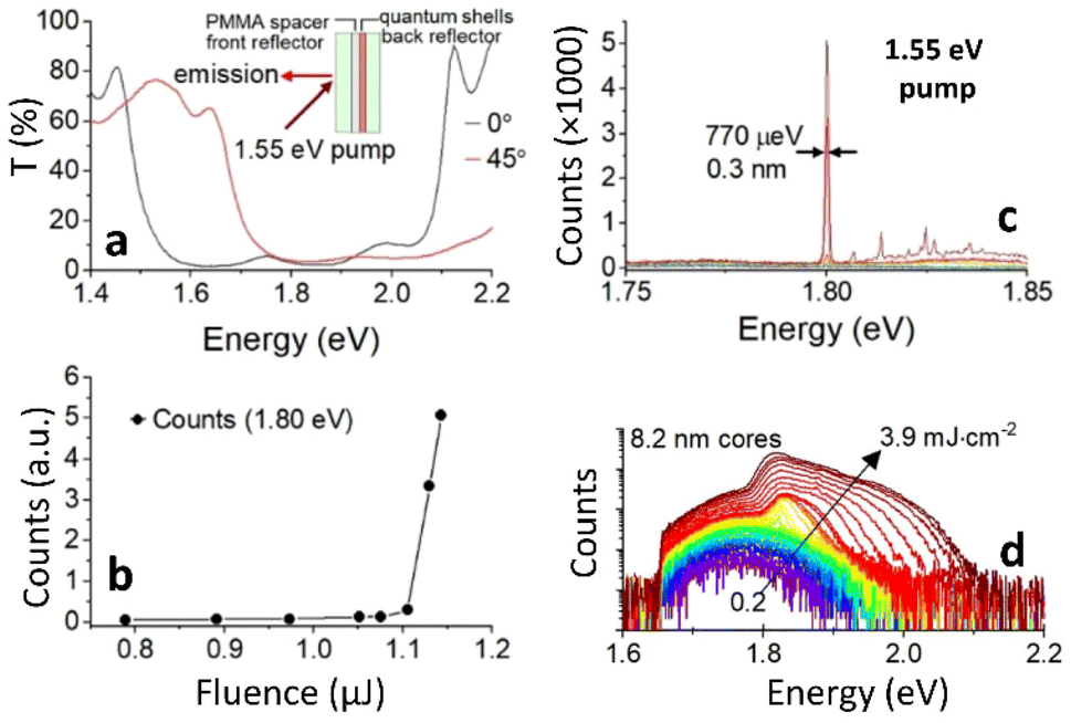 | ||
| Fig. 7 (a) Schematic illustrating the laser cavity's front window transmission for two-photon pumping of QS samples. The pump beam is incident at a 45° angle, while emission is collected normal to the surface, as shown in the inset. (b) Emission spectra from the laser cavity containing 8.2 nm core QSs, and (c) emission counts at 1.80 eV plotted as a function of 1.55 eV pump fluence. Violet spectra correspond to lower fluence, and red spectra represent higher fluence levels. (d) Amplified spontaneous emission spectra for CdS/CdSe/CdS QS thin films at varying pump fluences of 1.55 eV. A 750 nm short-pass filter was used to block pump light during measurements. Adapted with permission from ref. 32. Copyright 2023 The Royal Society of Chemistry. | ||
The laser exhibited a distinct threshold behavior, with a fluence threshold slightly above 1.1 mJ cm−2 (Fig. 7b), which just surpassed the ASE threshold for two-photon emission (Fig. 7d). This threshold is significantly lower than those previously reported for quantum dots (∼6 mJ cm−2),76 and is comparable to the lowest two-photon pumping thresholds observed in pure CdSe nanoplatelets (1.2 mJ cm−2)73 and dot-in-rod heterostructures (0.99 mJ cm−2).77 However, it remains somewhat higher than the thresholds for engineered CdSe core/shell structures (0.764 mJ cm−2)78 and perovskite nanocrystals (0.3 mJ cm−2).79 Further threshold reductions may be achievable through improvements in QS quantum yield, film uniformity, and cavity optimization.
Summary and outlook
The unique optical properties of colloidal quantum shells present a transformative opportunity for advancing lasing applications. By addressing a key limitation of colloidal nanocrystals, Auger recombination, these nanostructures offer a pathway to longer-lived optical gain, reduced heat generation, and enhanced device stability. Moreover, the slow Auger decay of multiexciton states in QSs unlocks the possibility for broader spectral amplification. As highlighted in this review, CdS–CdSe–CdS QSs have already demonstrated promising performance in both quasi-CW and two-photon upconverted laser systems, showcasing their ability to achieve efficient light amplification. The next steps in the development of QS gain media will likely focus on two critical challenges: the realization of electrically pumped laser diodes and the expansion of their spectral amplification capabilities into blue and infrared regimes.Electrically pumped laser diodes have long been a sought-after goal in the realm of colloidal nanostructures, but the path has been fraught with challenges. Achieving optical gain typically requires current densities of around 20 A cm−2,80 which leads to Auger heating and subsequent thermal degradation of the material. The QS architecture, with its intrinsic ability to suppress Auger recombination, offers a promising solution to this issue. By minimizing heat generation, QS-based devices could endure the high current densities required for lasing, a feat that parallels the exceptional stability observed in QS-based X-ray scintillators,33 underscoring the importance of reducing Auger heating in optoelectronic applications.
Another exciting frontier lies in expanding the spectral tunability of QSs to broaden their range of lasing applications. Current systems predominantly utilize CdSe quantum wells, which excel in the visible range. However, substituting these with materials like blue-emitting ZnSe or infrared-emitting HgS could push the emission spectrum into the ultraviolet and infrared regions. Such versatility would address the growing demands in fields ranging from bioimaging to optical communication and advanced sensing technologies, where precise spectral control is critical.
Data availability
No new software, experimental data, or code was generated or used for analysis in this review.Conflicts of interest
There are no conflicts to declare.Acknowledgements
This work was supported by the NSF Award #2208834. The authors acknowledge the financial support of the University of Michigan College of Engineering and NSF grant #DMR-9871177, and technical support from the Michigan Center for Materials Characterization. AW and MZ acknowledges the support by DE-SC0016872 funded by the U.S. Department of Energy, Office of Science.References
- A. V. Krishnamoorthy and K. W. Goossen, IEEE J. Quantum Electron., 1998, 4, 899–912 CAS.
- C. Grivas and M. Pollnau, Laser Photonics Rev., 2012, 6, 419–462 CrossRef.
- W. Xie, T. Stöferle, G. Rainò, T. Aubert, S. Bisschop, Y. Zhu, R. F. Mahrt, P. Geiregat, E. Brainis, Z. Hens and D. Van Thourhout, Adv. Mater., 2017, 29, 1604866 Search PubMed.
- D. Van Thourhout, T. Spuesens, S. K. Selvaraja, L. Liu, G. Roelkens, R. Kumar, G. Morthier, P. Rojo-Romeo, F. Mandorlo, P. Regreny, O. Raz, C. Kopp and L. Grenouillet, IEEE J. Quantum Electron., 2010, 16, 1363–1375 CAS.
- Y.-S. Park, J. Roh, B. T. Diroll, R. D. Schaller and V. I. Klimov, Nat. Rev. Mater., 2021, 6, 382–401 CrossRef CAS.
- C. Vannahme, S. Klinkhammer, U. Lemmer and T. Mappes, Opt. Express, 2011, 19, 8179 CrossRef CAS.
- C. B. Murray, D. J. Norris and M. G. Bawendi, J. Am. Chem. Soc., 1993, 115, 8706–8715 CrossRef CAS.
- C. R. Kagan, E. Lifshitz, E. H. Sargent and D. V. Talapin, Science, 2016, 353, 5523 CrossRef PubMed.
- V. I. Klimov, A. A. Mikhailovsky, S. Xu, A. Malko, J. A. Hollingsworth, C. A. Leatherdale, H.-J. Eisler and M. G. Bawendi, Science, 2000, 290, 314–317 CrossRef CAS PubMed.
- N. Ahn, C. Livache, V. Pinchetti and V. I. Klimov, Chem. Rev., 2023, 123, 8251–8296 Search PubMed.
- X. Peng, L. Manna, W. Yang, J. Wickham, E. Scher, A. Kadavanich and A. P. Alivisatos, Nature, 2000, 404, 59–61 CrossRef CAS PubMed.
- W. K. Bae, Y.-S. Park, J. Lim, D. Lee, L. A. Padilha, H. McDaniel, I. Robel, C. Lee, J. M. Pietryga and V. I. Klimov, Nat. Commun., 2013, 4, 2661 CrossRef PubMed.
- S. J. W. Vonk and F. T. Rabouw, J. Phys. Chem. Lett., 2023, 14, 5353–5361 CrossRef CAS PubMed.
- W. K. Bae, L. A. Padilha, Y.-S. Park, H. McDaniel, I. Robel, J. M. Pietryga and V. I. Klimov, ACS Nano, 2013, 7, 3411–3419 Search PubMed.
- Y.-S. Park, W. K. Bae, T. Baker, J. Lim and V. I. Klimov, Nano Lett., 2015, 15, 7319–7328 CrossRef CAS.
- F. Fan, O. Voznyy, R. P. Sabatini, K. T. Bicanic, M. M. Adachi, J. R. McBride, K. R. Reid, Y.-S. Park, X. Li, A. Jain, R. Quintero-Bermudez, M. Saravanapavanantham, M. Liu, M. Korkusinski, P. Hawrylak, V. I. Klimov, S. J. Rosenthal, S. Hoogland and E. H. Sargent, Nature, 2017, 544, 75–79 CrossRef CAS.
- J. Lim, Y.-S. Park and V. I. Klimov, Nat. Mater., 2018, 17, 42–49 CrossRef CAS PubMed.
- N. Ahn, C. Livache, V. Pinchetti, H. Jung, H. Jin, D. Hahm, Y.-S. Park and V. I. Klimov, Nature, 2023, 617, 79–85 CrossRef CAS.
- N. Ahn, C. Livache, V. Pinchetti and V. I. Klimov, Colloidal Semiconductor Nanocrystal Lasers and Laser Diodes, Chem. Rev., 2023, 123, 8251–8296 CrossRef CAS PubMed.
- S. Ithurria, M. D. Tessier, B. Mahler, R. P. S. M. Lobo, B. Dubertret and Al. L. Efros, Nat. Mater., 2011, 10, 936–941 CrossRef CAS PubMed.
- X. Ma, B. T. Diroll, W. Cho, I. Fedin, R. D. Schaller, D. V. Talapin, S. K. Gray, G. P. Wiederrecht and D. J. Gosztola, ACS Nano, 2017, 11, 9119–9127 CrossRef CAS PubMed.
- X. Ma, B. T. Diroll, W. Cho, I. Fedin, R. D. Schaller, D. V. Talapin, S. K. Gray, G. P. Wiederrecht and D. J. Gosztola, Size-Dependent Biexciton Quantum Yields and Carrier Dynamics of Quasi-Two-Dimensional Core/Shell Nanoplatelets, ACS Nano, 2017, 11, 9119–9127 CrossRef CAS PubMed.
- N. Razgoniaeva, P. Moroz, M. Yang, D. S. Budkina, H. Eckard, M. Augspurger, D. Khon, A. N. Tarnovsky and M. Zamkov, J. Am. Chem. Soc., 2017, 139, 7815–7822 CrossRef CAS PubMed.
- G. Nagamine, B. G. Jeong, T. A. C. Ferreira, J. H. Chang, K. Park, D. C. Lee, W. K. Bae and L. A. Padilha, ACS Photonics, 2020, 7, 2252–2264 CrossRef.
- J. Cassidy, B. T. Diroll, N. Mondal, D. B. Berkinsky, K. Zhao, D. Harankahage, D. Porotnikov, R. Gately, D. Khon, A. Proppe, M. G. Bawendi, R. D. Schaller, A. V. Malko and M. Zamkov, ACS Nano, 2022, 16, 3017–3026 CrossRef PubMed.
- A. H. Proppe, K. L. K. Lee, C. L. Cortes, M. Saif, D. B. Berkinsky, T. Sverko, W. Sun, J. Cassidy, M. Zamkov, T. Kim, E. Jang, S. K. Gray, B. A. McGuire and M. G. Bawendi, Phys. Rev. B, 2022, 106, 045425 CrossRef.
- J. Cassidy, D. Harankahage, D. Porotnikov, A. V. Malko and M. Zamkov, ACS Energy Lett., 2022, 7, 1202–1213 CrossRef.
- D. Harankahage, J. Cassidy, J. Beavon, J. Huang, N. Brown, D. B. Berkinsky, A. Marder, B. Kayira, M. Montemurri, P. Anzenbacher, R. D. Schaller, L. Sun, M. G. Bawendi, A. V. Malko, B. T. Diroll and M. Zamkov, J. Am. Chem. Soc., 2023, 145, 13326–13334 CrossRef.
- A. A. Marder, J. Cassidy, D. Harankahage, J. Beavon, L. Gutiérrez-Arzaluz, O. F. Mohammed, A. Mishra, A. C. Adams, J. D. Slinker, Z. Hu, S. Savoy, M. Zamkov and A. V. Malko, ACS Mater. Lett., 2023, 5, 1411–1419 Search PubMed.
- K. Zhao, X. Zhou, X. Li, J. Moon, J. Cassidy, D. Harankahage, Z. Hu, S. M. Savoy, Q. Gu, M. Zamkov and A. V. Malko, ACS Nano, 2024, 18, 10946–10953 CrossRef.
- I. Tanghe, K. Molkens, T. Vandekerckhove, D. Respekta, A. Waters, J. Huang, J. Beavon, D. Harankahage, C. Y. Lin, K. Chen, D. Van Thourhout, M. Zamkov and P. Geiregat, ACS Nano, 2024, 18, 14661–14671 CrossRef PubMed.
- B. T. Diroll, J. P. Cassidy, D. Harankahage, M. Hua, X.-M. Lin and M. Zamkov, Nanoscale, 2023, 15, 18415–18422 RSC.
- B. Guzelturk, B. T. Diroll, J. P. Cassidy, D. Harankahage, M. Hua, X.-M. Lin, V. Iyer, R. D. Schaller, B. J. Lawrie and M. Zamkov, Nat. Commun., 2024, 15, 4274 Search PubMed.
- J. Beavon, J. Huang, D. Harankahage, M. Montemurri, J. Cassidy and M. Zamkov, Chem. Commun., 2023, 59, 11337–11348 Search PubMed.
- E. P. Pokatilov, V. A. Fonoberov, V. M. Fomin and J. T. Devreese, Phys. Rev. B: Condens. Matter Mater. Phys., 2001, 64, 245329 Search PubMed.
- E. A. Dias, J. I. Saari, P. Tyagi and P. Kambhampati, J. Phys. Chem. C, 2012, 116, 5407–5413 CrossRef.
- M. Braun, S. Link, C. Burda and M. El-Sayed, Chem. Phys. Lett., 2002, 361, 446–452 CrossRef.
- J. Xu and M. Xiao, Appl. Phys. Lett., 2005, 87, 173117 CrossRef.
- J. Xu, M. Xiao, D. Battaglia and X. Peng, Appl. Phys. Lett., 2005, 87, 043107 CrossRef.
- D. Battaglia, J. J. Li, Y. Wang and X. Peng, Angew. Chem., Int. Ed., 2003, 42, 5035–5039 CrossRef PubMed.
- B. G. Jeong, Y.-S. Park, J. H. Chang, I. Cho, J. K. Kim, H. Kim, K. Char, J. Cho, V. I. Klimov, P. Park, D. C. Lee and W. K. Bae, ACS Nano, 2016, 10, 9297–9305 CrossRef.
- Y. S. Park, J. Roh, B. T. Diroll, R. D. Schaller and V. I. Klimov, Nat. Rev. Mater., 2021, 6, 382–401 CrossRef.
- J. Cassidy, D. Harankahage, J. Ojile, D. Porotnikov, L. Walker, M. Montemurri, B. S. L. Narvaez, D. Khon, M. D. E. Forbes and M. Zamkov, Chem. Mater., 2022, 34, 2484–2494 CrossRef.
- B. Yuan and L. Cademartiri, Growth of Colloidal Nanocrystals by Liquid–Like Coalescence, Angew. Chem., Int. Ed., 2021, 60(12), 6667–6672 CrossRef.
- E. J. Endres, J. R. B. Espano, A. Koziel, A. R. Peng, A. A. Shults and J. E. Macdonald, Controlling Phase in Colloidal Synthesis, ACS Nanosci. Au, 2024, 4(3), 158–175 CrossRef.
- M. J. Kim, J. J. Lee, S. H. Lee and S. H. Sohn, Study of CdTe/CdS Heterostructure by CdCl2 Heat Treatment via in situ High Temperature XRD, Sol. Energy Mater. Sol. Cells, 2013, 109, 209–214 CrossRef.
- B. E. McCandless, L. V. Moulton and R. W. Birkmire, Recrystallization and Sulfur Diffusion in CdCl2-Treated CdTe/CdS Thin Films, Prog. Photovoltaics: Res. Appl., 1997, 5, 249–260 CrossRef.
- J. Cassidy, C. Ellison, J. Bettinger, M. Yang, P. Moroz and M. Zamkov, Enabling Narrow Emission Linewidths in Colloidal Nanocrystals through Coalescence Growth, Chem. Mater., 2020, 32, 7524–7534 CrossRef.
- J. Cassidy, M. Yang, D. Harankahage, D. Porotnikov, P. Moroz, N. Razgoniaeva, C. Ellison, J. Bettinger, S. Ehsan, J. Sanchez, J. Madry, D. Khon and M. Zamkov, Nano Lett., 2021, 21, 7339–7346 CrossRef.
- Y.-S. Park, W. K. Bae, J. M. Pietryga and V. I. Klimov, ACS Nano, 2014, 8, 7288–7296 CrossRef PubMed.
- A. P. Beyler, T. S. Bischof, J. Cui, I. Coropceanu, D. K. Harris and M. G. Bawendi, Nano Lett., 2014, 14, 6792–6798 CrossRef.
- G. Nair, J. Zhao and M. G. Bawendi, Nano Lett., 2011, 11, 1136–1140 CrossRef PubMed.
- B. D. Mangum, S. Sampat, Y. Ghosh, J. A. Hollingsworth, H. Htoon and A. V. Malko, Nanoscale, 2014, 6, 3712 RSC.
- X. Dai, Y. Deng, X. Peng and Y. Jin, Adv. Mater., 2017, 29, 1607022 CrossRef PubMed.
- G. Azzellino, F. S. Freyria, M. Nasilowski, M. G. Bawendi and V. Bulović, Adv. Mater. Technol., 2019, 4, 1800727 CrossRef.
- J. Roh, Y.-S. Park, J. Lim and V. I. Klimov, Nat. Commun., 2020, 11, 271 CrossRef.
- Z. Meng, B. Mahler, J. Houel, F. Kulzer, G. Ledoux, A. Vasil'ev and C. Dujardin, Nanoscale, 2021, 13, 19578–19586 RSC.
- Y. Zhou, J. Chen, O. M. Bakr and O. F. Mohammed, ACS Energy Lett., 2021, 6, 739–768 CrossRef CAS.
- F. Fan, O. Voznyy, R. P. Sabatini, K. T. Bicanic, M. M. Adachi, J. R. McBride, K. R. Reid, Y.-S. Park, X. Li, A. Jain, R. Quintero-Bermudez, M. Saravanapavanantham, M. Liu, M. Korkusinski, P. Hawrylak, V. I. Klimov, S. J. Rosenthal, S. Hoogland and E. H. Sargent, Nature, 2017, 544, 75–79 CrossRef CAS PubMed.
- S. A. Ivanov, J. Nanda, A. Piryatinski, M. Achermann, L. P. Balet, I. V. Bezel, P. O. Anikeeva, S. Tretiak and V. I. Klimov, J. Phys. Chem. B, 2004, 108, 10625–10630 CrossRef.
- C. Dang, J. Lee, C. Breen, J. S. Steckel, S. Coe-Sullivan and A. Nurmikko, Nat. Nanotechnol., 2012, 7, 335–339 CrossRef.
- V. I. Klimov, S. A. Ivanov, J. Nanda, M. Achermann, I. Bezel, J. A. McGuire and A. Piryatinski, Nature, 2007, 447, 441–446 Search PubMed.
- I. Tanghe, M. Samoli, I. Wagner, S. A. Cayan, A. H. Khan, K. Chen, J. Hodgkiss, I. Moreels, D. V. Thourhout, Z. Hens and P. Geiregat, Nat. Nanotechnol., 2023, 18, 1423–1429 Search PubMed.
- M. Chen, L. Lu, H. Yu, C. Li and N. Zhao, Adv. Sci., 2021, 8, 2101560 Search PubMed.
- N. Ahn, C. Livache, V. Pinchetti and V. I. Klimov, Chem. Rev., 2023, 123, 8251–8296 Search PubMed.
- Y.-S. Park, J. Roh, B. T. Diroll, R. D. Schaller and V. I. Klimov, Nat. Rev. Mater., 2021, 6, 382–401 CrossRef.
- W. Xie, T. Stöferle, G. Rainò, T. Aubert, S. Bisschop, Y. Zhu, R. F. Mahrt, P. Geiregat, E. Brainis, Z. Hens and D. Van Thourhout, Adv. Mater., 2017, 29, 1604866 CrossRef PubMed.
- F. Fan, O. Voznyy, R. P. Sabatini, K. T. Bicanic, M. M. Adachi, J. R. McBride, K. R. Reid, Y.-S. Park, X. Li, A. Jain, R. Quintero-Bermudez, M. Saravanapavanantham, M. Liu, M. Korkusinski, P. Hawrylak, V. I. Klimov, S. J. Rosenthal, S. Hoogland and E. H. Sargent, Nature, 2017, 544, 75–79 CrossRef PubMed.
- F. Helmchen and W. Denk, Nat. Methods, 2005, 2, 932–940 CrossRef PubMed.
- G. S. He, L.-S. Tan, Q. Zheng and P. N. Prasad, Chem. Rev., 2008, 108, 1245–1330 CrossRef.
- Q. Zheng, H. Zhu, S.-C. Chen, C. Tang, E. Ma and X. Chen, Nat. Photonics, 2013, 7, 234–239 CrossRef.
- B. Guzelturk, Y. Kelestemur, K. Gungor, A. Yeltik, M. Z. Akgul, Y. Wang, R. Chen, C. Dang, H. Sun and H. V. Demir, Adv. Mater., 2015, 27, 2741–2746 CrossRef PubMed.
- M. Li, M. Zhi, H. Zhu, W.-Y. Wu, Q.-H. Xu, M. H. Jhon and Y. Chan, Nat. Commun., 2015, 6, 8513 CrossRef PubMed.
- B. Guzelturk, Y. Kelestemur, M. Olutas, S. Delikanli and H. V. Demir, ACS Nano, 2014, 8, 6599–6605 CrossRef PubMed.
- L. Xu, Y. Meng, C. Xu and P. Chen, RSC Adv., 2018, 8, 36910–36914 RSC.
- B. Guzelturk, Y. Kelestemur, M. Z. Akgul, V. K. Sharma and H. V. Demir, J. Phys. Chem. Lett., 2014, 5, 2214–2218 CrossRef CAS PubMed.
- G. Xing, Y. Liao, X. Wu, S. Chakrabortty, X. Liu, E. K. L. Yeow, Y. Chan and T. C. Sum, ACS Nano, 2012, 6, 10835–10844 CrossRef CAS PubMed.
- B. Guzelturk, Y. Kelestemur, K. Gungor, A. Yeltik, M. Z. Akgul, Y. Wang, R. Chen, C. Dang, H. Sun and H. V. Demir, Adv. Mater., 2015, 27, 2741–2746 CrossRef CAS.
- Z. Liu, Z. Hu, Z. Zhang, J. Du, J. Yang, X. Tang, W. Liu and Y. Leng, ACS Photonics, 2019, 6, 3150–3158 CrossRef CAS.
- O. V. Kozlov, Y.-S. Park, J. Roh, I. Fedin, T. Nakotte and V. I. Klimov, Sub-Single-Exciton Lasing Using Charged Quantum Dots Coupled to a Distributed Feedback Cavity, Science, 2019, 365, 672–675 CrossRef.
| This journal is © The Royal Society of Chemistry 2025 |