
 Open Access Article
 This Open Access Article is licensed under a
 Creative Commons Attribution 3.0 Unported Licence
Molecularly-anchored single PbS quantum dots as resonant tunnelling transistors†
Retno Dwi
Wulandari
 abc,
Dongbao
Yin
a,
Ricky Dwi
Septianto
bc,
Seiichiro
Izawa
a,
Yoshihiro
Iwasa
b,
Satria Zulkarnaen
Bisri
*bc and
Yutaka
Majima
*a
abc,
Dongbao
Yin
a,
Ricky Dwi
Septianto
bc,
Seiichiro
Izawa
a,
Yoshihiro
Iwasa
b,
Satria Zulkarnaen
Bisri
*bc and
Yutaka
Majima
*a
aMaterials and Structures Laboratory, Institute of Integrated Research, Institute of Science Tokyo, 4259 Nagatsuta-cho, Midori-ku, Yokohama, Kanagawa 226-8503, Japan. E-mail: majima@msl.titech.ac.jp
bRIKEN Center for Emergent Matter Science (CEMS), 2-1 Hirosawa, Wako, Saitama 351-0198, Japan
cDepartment of Applied Physics and Chemical Engineering, Tokyo University of Agriculture and Technology, 2-24-16 Nakacho, Koganei, Tokyo 184-8588, Japan. E-mail: satria-bisri@go.tuat.ac.jp
First published on 3rd February 2025
Abstract
The growing need for high-performance computing continues to drive improvement in circuit and device technologies, particularly with respect to speed and power efficiency. Device scaling remains the most effective strategy for meeting circuit performance requirements while reducing power consumption. Thanks to their solution processability, colloidal semiconductor quantum dots (QDs) are highly suitable for device miniaturisation as quantum information science platforms. Quantum mechanical effects must be carefully considered when designing nanometre-scale electronic devices (i.e., transistors) that incorporate a single QD. Here, we demonstrate a resonant tunnelling transistor (RTT) based on a single lead sulfide (PbS) QD anchored by a bidentate ligand molecule attached to heteroepitaxial spherical Au/Pt nanogap electrodes. Five negative differential resistances (NDRs) were observed at both positive and negative drain voltages in output characteristics, which could be attributed to the formation of a double-barrier “quantum well” structure with the strong Fermi level pinning of the discrete energy level of the QD to one electrode. Furthermore, these NDRs could be tuned by applying a gate electric field, which will become one of the keys for enabling quantum and neuromorphic electronics. This demonstration of single PbS-QD-based RTTs paves the way for sub-10 nm solution-processable quantum electronic devices.
Introduction
In recent years, the continuous scaling of semiconductor device technologies to improve speed and power has been the primary focus in device manufacturing, and has led to ultimately scaled feature sizes. The latest generation of core processors used in many computers utilises a tiny (10 nm) fin-field effect transistor (Fin-FET)1,2 technology, which works on the principle of a conventional FET. However, further shrinkage of the channel region in metal–oxide-semiconductor FET (MOSFETs) on bulk silicon substrates introduces short-channel effects, which challenges device performance by increasing leakage current and off-current.3 On the other hand, these binary devices (which have dominated the electronic industry and link the natural property of devices to being in the ON or OFF state with two logic levels) provide the least possible information content per interconnect.4 Multi-valued logic (MVL) has been considered to improve computation efficiency and reduce the power consumption of modern chips.5 MVL is a non-binary-valued system in which more than two levels of information content are available. Consequently, MVLs enable higher information density, allowing logic functions to be performed with fewer logic gates and interconnects.Negative differential resistance (NDR) is characterised by a decrease in drain current (ID) while the drain voltage (VD) increases. These NDR regions have been proposed to originate from resonant electron tunnelling through discrete energy levels in quantum well structures.6–9 Recently, NDR effects in semiconductors have attracted significant interest in developing high-frequency oscillators, high-speed logic, and memory devices.10–12 Importantly, multiple NDRs in resonant tunnelling transistors (RTTs) are particularly promising for proposed MVL applications due to their fast switching speed and the potential for device miniaturisation.13,14 Furthermore, the tunnelling mechanism in RTTs is advantageous because, unlike various conventional FETs, RTTs are predicted to not suffer from short-channel effects due to their tunnelling mechanism.15,16
Recent advances in the synthesis and technologies of advanced materials have restarted the interest in driving progress in the MVL field, alongside the urgency to make these technologies practical. Among all emerging materials (that also include van der Waals (vdW), organics, and oxide materials), colloidal semiconductor quantum dots (QDs) are among the best candidates for realising MVL devices. The recent development of well-defined synthetic procedures for certain QD compounds, along with their low-cost fabrication, makes colloidal QDs highly suitable to support device miniaturisation through solution processing, thereby positioning them as ideal candidates for new platforms in quantum information science.17,18
Colloidal QDs possess quantum confinement effects, which leads to the quantisation of their discrete energy levels and bandgap tunability by size.19,20 This quantum confinement effect is crucial for designing nanometre-scale electronic devices (i.e., transistors) that involve a single QD.21–23 The study of single colloidal QD devices has gained renewed attention in recent years due to their potential advanced electronic application. Recently, single PbS colloidal QDs have demonstrated significant advances, including the observation of single-electron transistor (SET) behaviour and even Kondo effects,21 highlighting their versatility in exploring quantum phenomena at the nanoscale. Additionally, using our unique electroless Au plating (ELGP) method of heteroepitaxial-spherical (HS) Au/Pt nanogap electrodes, we recently reported the coexistence of resonant tunnelling current and single-electron tunnelling current on a single cadmium sulphide (CdS) colloidal QD SET.24
HS-Au/Pt nanogap electrodes have been fabricated by combining ELGP with electron beam lithography (EBL), resulting in a fabrication yield of 90% without any short circuit.30–32 Au nanogap electrodes are commonly known to be thermally unstable owing to Rayleigh instability.25,26 Therefore, we introduced Pt as the base material for source and drain electrodes, with a 10 nm linewidth, to achieve large gate capacitance.27 Pt is a more suitable material because of its higher melting point and a surface diffusion coefficient that is 107 to 108 times smaller than that of Au.28 We then established the fabrication process of an ELGP HS-Au/Pt nanogap on a Pt-based nanogap, allowing the heteroepitaxial growth of Au on initial polycrystal Pt nanogap electrodes to decrease and control the gap separation for single QD devices29–31 (ESI Note 2†). Our ELGP is a unique method that enables the simultaneous fabrication of multiple nanogaps and precise control of the gap separation of nanogap electrodes.30,31
An essential strategy is a bottom–up approach to fabricating a high-quality single QD transistor based on the colloidal process that can be anchored between HS-Au/Pt nanogap electrodes. The HS-Au/Pt nanogap consists of one pair of Au spheres with small radii (<5 nm), so a single QD could be anchored using a thiol-based bidentate ligand to Au electrodes.24,30
The resonant tunnelling current coexists with the single-tunnelling electron tunnelling current on a single QD SET,24 so the resonant tunnelling current flows through the quantised energy levels of the QD and depends on the number of electrons on the QD. This is beneficial for implementing MVL devices. Nevertheless, challenges related to the conceptual fabrication of MVL devices require radical solutions.
Here, we demonstrate multiple NDRs in RTTs utilising a single lead sulfide (PbS) colloidal QD as its fundamental building block. PbS QDs were chosen for their well-established synthetic process and large electron Bohr radius. This provides robust and stable quantum confinement at the given QD diameters, leading to the well-defined formation of discrete energy levels. To effectively anchor the single QD between the nanogap electrodes, self-assembled monolayers (SAMs) of 1,2-ethanedithiol (EDT) and 1,4-butanedithiol (BuDT) were formed on the surface of our HS-Au/Pt nanogap electrodes. These ligands are critical for creating a strong and stable anchor between the QD and electrode, which is essential for enabling Fermi-level pinning and enhancing resonant tunnelling, ultimately leading to the observation of NDR. We discussed the properties of single PbS QD transistors, focusing on the multiple NDR features and Coulomb oscillations observed with and without dithiol anchoring. The role of dithiol anchoring was analysed, particularly in how it may help pin the QD Fermi level to the electrode as the possible mechanism of RTT operations.
Results and discussion
Device structure
A schematic illustration of a fabricated RTT structure is shown in Fig. 1a. A single PbS QD was present between HS-Au/Pt nanogap electrodes. The landing of the PbS QD on the surface of the SiO2/Si substrate allowed the 50 nm SiO2 dielectric to function as the back-gate of the RTT. We utilised a QD of diameter 8.1 nm as the quantum island with a narrow bandgap of 0.66 eV and a large Bohr exciton radius of 18 nm (Note 1, ESI, and Fig. S1 and S2†).33 This QD diameter has also been used to investigate the charge carrier transport in large-scale QD superlattice assemblies.34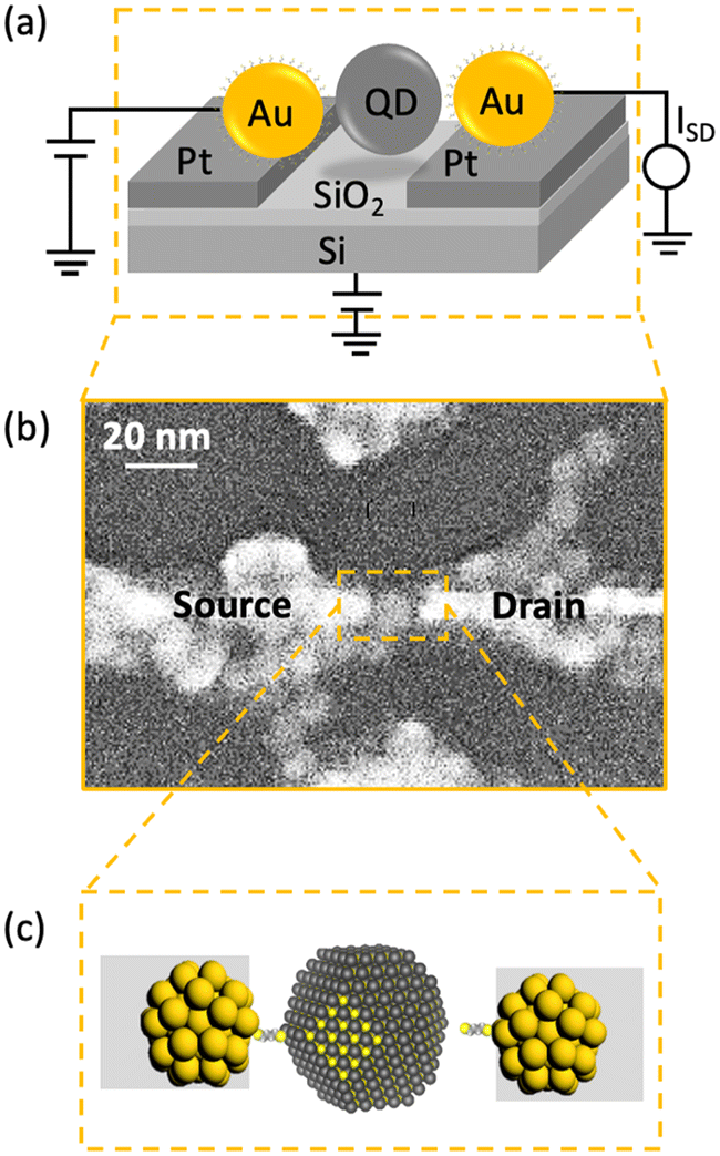 | ||
| Fig. 1 Resonant tunnelling transistor of a single PbS colloidal quantum dot. (a) Structure of a PbS QD RTT (schematic). (b) SEM image of ELGP HS-Au/Pt nanogap electrodes separated by a gap of ∼9 nm onto which PbS QDs (d ∼8.1 nm) have been one side-chemisorbed. (c) Simplified illustration of the magnified RTT with the top-view perspective. 1,2-ethanedithiol (EDT) is chemically anchored the PbS QD core to a spherical Au electrode. | ||
Appropriate selection of dithiol anchor molecules enables us to realise high-performance RTT based on a single PbS QD. It should be noted that PbS colloidal QDs are protectively capped by long and insulating native oleic acid (OAc) ligands. Ligand exchange in the solid-state is the viable way to replace these native oleic acid ligands with the desired anchoring ones.35 However, performing ligand exchange on the QD after it has landed between the nanogap electrode would be challenging due to the potential movement of the QDs during the exchange process.36
Therefore, we introduced a method that simultaneously exchanges the ligand and directly anchors the QD onto the HS-Au/Pt nanogap electrode. It was achieved by preparing EDT or BuDT SAM on the HS-Au/Pt nanogap electrode on which the QD will be anchored.37,38 The stronger affinity of the thiol-based bidentate ligands to the surface of the PbS QD than of the OAc enables the attachment of the PbS QD and replacement of the OAc.39–41 Consequently, the prepared nanogap separation should be designed to equal the sizes of the QD and the bidentate molecules. Fig. 1b shows the scanning electron microscope (SEM) image of the fabricated RTT with a PbS QD of 8.1 nm. The small gap between the QD and Au source electrode suggests anchoring by the alkane-dithiol molecule (in this case, EDT).
The two alkane-dithiol anchoring molecules with different chain lengths (BuDT and EDT) were expected to modulate the carrier transport of the RTT. The molecular lengths for EDT, BuDT, and OAc are 0.5 nm, 0.7 nm, and 2 nm, respectively, which change the distance between the QD and the Au electrode. Additionally, the ligand exchange process of oleic acid with thiol-based ligands alters the configurations of a single QD between the HS-Au/Pt nanogap electrode. The width of the tunnel barriers can be adjusted using these molecular ligands with different chain lengths, which varies the interaction between the discrete energy levels of QD and Au electrodes. The strong bonds between Au and the alkane-dithiol, as well as between the alkane-dithiol and the PbS QD, anchor the QD with the Au electrode, and Fermi-level pinning becomes strong by decreasing the chain length in the nanogap system.42–45 This combination of HS-Au/Pt nanogap electrodes and molecular anchoring resulted in a yield of working RTT of 1.3%.
Negative differential resistance in transport measurements
Low-temperature transport measurements of the transistors were performed in a cryogenic probe station at 9 K. The robustness of the ELGP HS-Au/Pt nanogap electrode allows for the application of a relatively high electrical drain bias voltage (VD) across the source and the drain electrodes, up to 3 V, without Au atom migration. To modulate the electronic state of the PbS QDs in the transistor, we utilised only the back-gate voltage through SiO2 (50 nm). Fig. 2a shows the 9 K ID–VD characteristics of the PbS QD RTT, which used a 0.7 nm BuDT ligand under the application of different back-gate voltages (VG) from −3.00 V to −2.72 V. This device exhibited decreases in its ID as the VD increased at some VD regions, alongside a generally monotonous increase in ID. Five negative differential resistance (NDR) phenomena were observed in the PbS QD RTT in both positive and negative VD regions. We also measured the ID–VD characteristics under forward and backward sweeps (Fig. S4†). Even the peak and valley VD changed slightly due to charge trapping around the QD; the same number (5) of NDR phenomena were observed on forward and backward sweeps. It should be noted that NDR phenomena are absent in conventional QD assembly FETs34,36,39,41,46 and the recently reported single PbS QD SET.21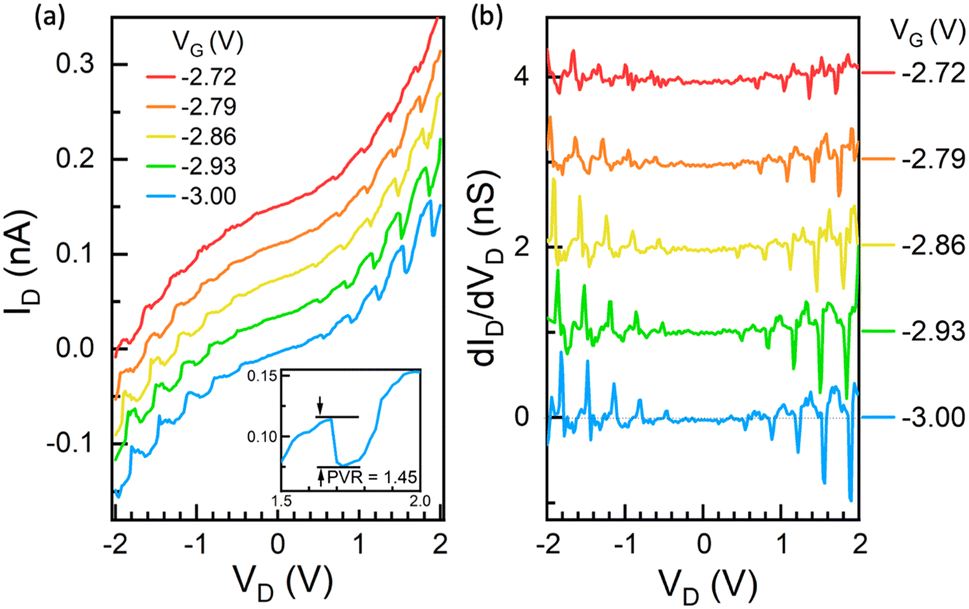 | ||
| Fig. 2 Negative differential resistance (NDR) in a single PbS QD resonant tunnelling transistor. (a) The measured current–voltage (ID–VD) characteristics of a 1,4-butane dithiol (BuDT)-anchored PbS QD transistor at T = 9 K, taken at every 70 mV step of the back-gate voltage (VG), showing multiple NDR peaks in both negative and positive drain voltage (VD) regimes. (b) The corresponding dID/dVD–VD characteristics. The VG dependence of differential conductance dID/dVD was numerically calculated based on the experimental ID–VD characteristics, showing the electronic states of PbS QD. For clarity, the ID–VD and dID/dVD–VD characteristics are offset by 37.5 pA and 1 nS, respectively. Only the bottom curves at VG = −3.0 V correspond to the actual scale. | ||
We then estimated the ratio of the current at the resonant tunnelling peak to that at the valley before the current started to increase again with voltage, commonly referred to as the peak-to-valley ratio (PVR). The latter is a widely used metric for measuring NDR performance. PVR values were calculated at five distinct NDR peaks as 1.32, 1.27, 1.35, 1.32, and 1.45 (Fig. S6†). Although smaller than that in single-molecule transistor-based47 and molecular monolayer-based48 NDR devices, which can achieve a PVR of over 30 and 100, respectively, to our knowledge, multiple (5) NDRs and this PVR value are the first ever reported for a single-QD RTT.
Due to the capability to apply a large bias voltage ranging from −2 V to 2 V, we could observe multiple periods of NDR features in both positive and negative VD regimes. Five NDR periods are available in both regimes, which can be used in five multi-logic states within this VD range.
We plotted the differential conductance dID/dVD of the QD device for different values of applied VG to highlight the peaks and valleys of NDR behaviour (Fig. 2b). The origin of the observed NDR was fundamentally tied to the discrete energy levels in the PbS QD and the alignment of these energy levels with the Fermi levels of the source/drain electrodes. The nearly periodic peak-to-peak voltages of the NDRs (approximately 290–360 mV) reflected the interplay between Coulomb blockade effects and the degeneracy of the 1S level in the PbS QD.
Unlike Cd- or Hg-chalcogenides, which exhibit single degeneracy,49 lead chalcogenides, such as PbS, have an intriguing band structure with the fundamental gap located at the L-point of the Brillouin zone.50–52 Therefore, they have four-fold valley degeneracy. The characteristics of valley degeneracy of the compound can be translated into the multiplicity of the energy levels in single QD devices. This occurrence has been observed in single Si QD devices.53–55
Therefore, the PbS QD can lead to quantum-confined levels with a four-fold34,41,56 higher multiplicity than materials like CdS QD. Eight electrons can occupy four-fold valley degeneracy. Our observation of five equally spaced resonances, corresponding to the sequential filling of the eight-fold degenerate electron level, confirmed the higher multiplicity of PbS energy levels. This high degeneracy allows for multiple NDR features as the voltage varies, reflecting the periodic alignment of these degenerate states with the electrode Fermi level, resulting in periodic NDR spacing. Our results on equally spaced peak-to-peak features are consistent with previous reports on another lead chalcogenide with four-fold degeneracy, specifically PbSe QDs.57,58 Importantly, by using ELGP HS-Au/Pt nanogap electrodes, we could apply a broader voltage range, enabling us to access more resonance peaks.
In contrast to II–VI semiconductors, the effective masses of electrons and holes are nearly equal, leading to symmetric conduction and valence bands. The two lowest levels in this structure had S and P envelope symmetry, respectively. The measured tunnelling spectrum reflected the symmetric levels scheme (Fig. 2b and Fig. S5†).
The observation of NDRs in the measured ID–VD characteristics strongly indicated that this sample operated as an RTT. To highlight the reproducibility of these features, we presented similar NDR phenomena in another transistor (Note 4, ESI†), which exhibited well-pronounced multiple NDR properties in positive and negative VD bias regimes (Fig. S7†), with PVR values of 1.39, 1.33, 1.29, 1.23, and 1.27 (Fig. S8†).
Replacing BuDT with shorter bidentate thiol ligands, such as EDT, could enhance the coupling between the Au electrodes and PbS QD. Notably, the measured ID–VD characteristics of these EDT-anchored devices also exhibited NDR properties in both positive and negative VD regions (Fig. S9†). The differential conductance as a function of gate voltage also indicated the NDR feature, with a slight shift towards positive VD as VG decreased. A comparable shift in the NDR peaks was also observed in BuDT-anchored devices (Fig. 2b), confirming that both devices underwent effective gate modulation. The observations of NDR features in these two sets of RTTs demonstrated that pinning the QD Fermi level to the electrode using strong bonding between bidentate thiol molecules and Au was crucial for achieving resonant tunnelling transport.
Measurement of Coulomb oscillation in transport
Another feature of these RTTs was the observation of Coulomb oscillation in their ID–VG characteristics. Fig. 3a shows the BuDT-anchored QD RTT ID as a function of the applied VG. Instead of a monotonous increase in the ID–VG characteristics, we observed clear Coulomb oscillations. As shown in Fig. 2a, Coulomb blockade phenomena were not observed in ID–VD characteristics. However, Coulomb oscillation behaviours were observed. Each Coulomb oscillation peak indicated a change in the number of electrons in the PbS QD, with one electron tunnelling through different energy levels. The discrete energy levels of the QD and the well-defined double barrier tunnelling junction structure of the RTT allowed observation of these Coulomb oscillations. Over a VG modulation range of 2.7 V (−5 V < VG < −2.3 V), six Coulomb oscillation peaks were observed with a peak-to-peak VG difference (ΔVG) of ∼0.5 V. In addition to BuDT, we utilised the shorter dithiol ligand, EDT, as shown in Fig. 3b. Within the same range of applied VG (2.7 V) on the EDT-anchored QD RTT, approximately six Coulomb oscillation peaks were observed, similar to the number seen in the BuDT-anchored QD RTT. This similarity could later be observed in the number of parallel lines in Fig. 4.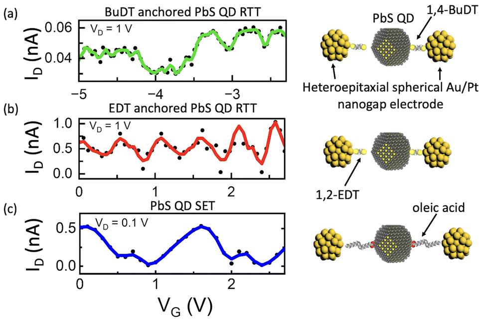 | ||
| Fig. 3 Coulomb oscillations in different PbS QD transistors. The measured drain current–gate voltage (ID–VG) characteristics of PbS QDs transistor devices with different ligand molecules. The ligand molecules have different lengths (l) and relative permittivity (εr): (a) 1,4-butanedithiol (BuDT) (l = 0.7 nm and εr = 12), (b) 1,2-ethanedithiol (EDT) (l = 0.5 nm and εr = 12), and (c) the native oleic acid (l = 2 nm and εr = 2.85). In devices (a) and (b), each ligand molecule has two thiol end moieties, which are chemically anchored to PbS QD and Au one electrode. In contrast, in device (c), oleic acid molecules bind only to the PbS QD and are merely physisorbed between the HS-Au/Pt nanogap electrodes. | ||
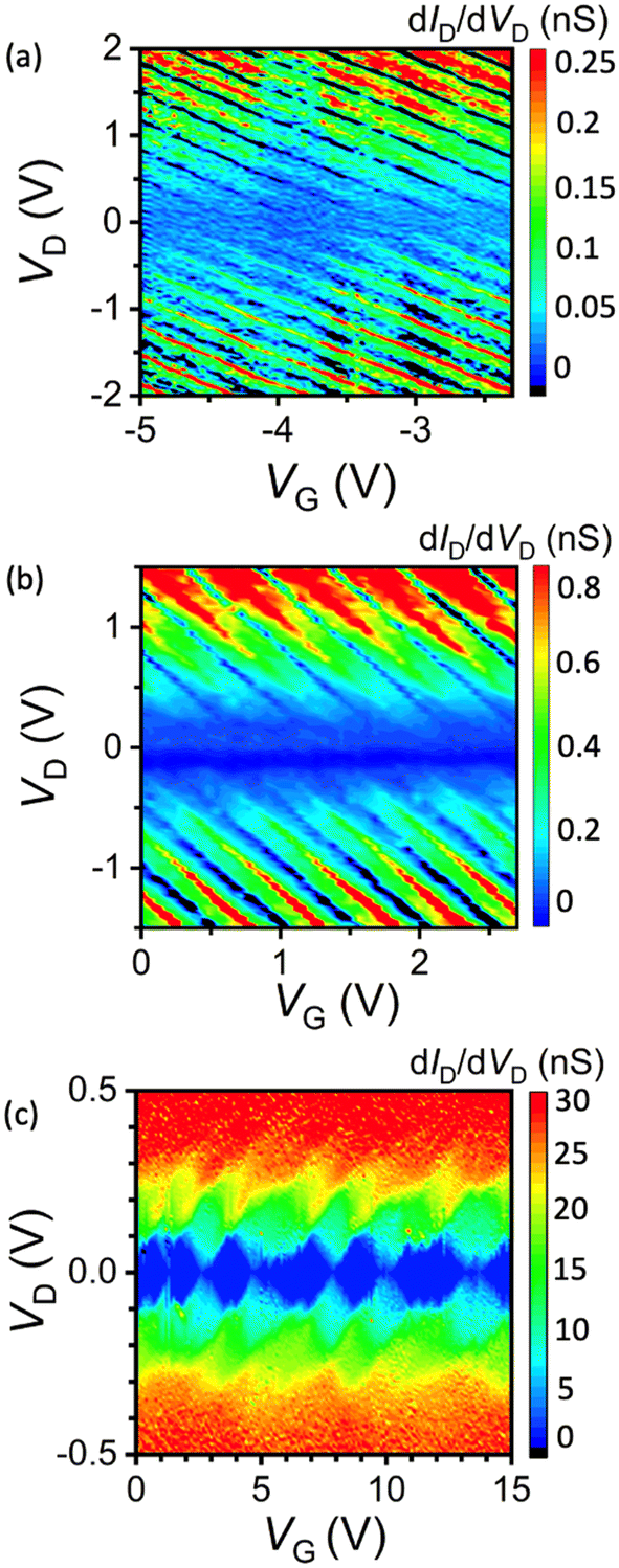 | ||
| Fig. 4 2D dID/dVD mapping of PbS QD transistors. Contour mapping stability diagrams were obtained by plotting colour maps of dID/dVD as functions of VD and VG for (a) 1,4-Butanedithiol (BuDT)-anchored PbS QD RTT, (b) 1,2-ethanedithiol (EDT)-anchored PbS QD RTT, and (c) oleic acid-capped PbS QD SET. All measurements were carried out at T = 9 K. | ||
In contrast, Fig. 3c shows the corresponding ID–VG transfer characteristics of PbS QD capped with molecules with carboxylic acid moieties, i.e., oleic acid (OAc), which exhibited a much smaller number of Coulomb oscillations. Within the similar VG range, only two peaks were observed, with a peak-to-peak VG difference of approximately 1.5 V. A similar number of Coulomb oscillation peaks was reproducibly observed in another set of OAc-capped PbS QD devices (Fig. S10†).
The number of Coulomb oscillations directly determines the number of possible logic states that can be generated. A higher number of logic states can be achieved within the same VG range if the spacing between oscillation peaks (ΔVG) is smaller. In other words, a small ΔVG is preferable for creating logic states.
Discussion
The 2D (VD and VG) differential conductance (dID/dVD) plots, so-called “stability diagrams”, provide a better representation of the electrical properties of the PbS QD RTTs and SETs. Fig. 4a shows the stability diagram of the BuDT-anchored PbS QD device. Although Coulomb diamonds were not observed, parallel conductance lines from the upper-left to lower-right were observed. In PbS QD RTTs, two tunnelling junctions were present between the HS-Au/Pt nanogap and PbS QD core. Coulomb blockade was not observed, implying the tunnelling resistance between the PbS QD core and the Au one electrode anchored by the BuDT was lower than the quantum resistance (h/e2 (= 25.8 kΩ), h = Planck constant, e = unit charge).59 With the total resistance of the BuDT-anchored PbS QD RTT exceeding 1 GΩ, the other tunnelling resistance was approximately equal to the total resistance of the PbS QD RTT. It suggests the Fermi energy levels of the PbS QD were pinned to that of the source or drain electrode at the BuDT-anchored tunnelling junction.On the larger tunnelling junction side, either at the source or the drain electrodes, a resonant tunnelling current flowed when the Fermi level of the electrode aligned with the available pinned discrete energy levels of the QD. This alignment enhanced the tunnelling current, which appeared as parallel red conductance line features corresponding to the NDR peaks.
Meanwhile, parallel black lines (dID/dVD < 0) were observed between these red parallel conductance lines, which corresponded to the NDR valleys. These valleys occur if the alignment between the Fermi level of the electrode and the pinned discrete energy level is disrupted.
The stability diagram also showed parallel red and black line patterns for the EDT-anchored PbS QD device, suggesting RTT operation (Fig. 4b). This device demonstrated wider conductance peak-to-peak VG periods and higher conductance values than those of BuDT-anchored PbS QD.
The well-defined NDRs and Coulomb oscillations observed over a broad range of VD and ID in these bidentate ligand-anchored PbS QD transistors confirmed their operation as robust RTTs. This phenomenon also provided the most plausible explanation for the multiple parallel lines in the stability diagrams (Fig. 4a and b). The strong anchoring of PbS QDs to the HS-Au/Pt electrode using bidentate molecular ligands pins the QD Fermi energy level to the electrode. Consequently, the NDRs and Coulomb oscillations arise from quantum tunnelling and the quantised electron occupancy of the QD, which contain multiple resonant states or energy levels. Under specific bias conditions, tunnelling occurs through discrete energy levels within the quantum well structure of the device, producing NDRs and Coulomb oscillation regions.
These observations are challenging to interpret within the conventional framework of single-electron transistors (SETs). Studies on single PbS QD21 or Si QD53 transistors have predominantly utilised relatively long ligands to couple the QD with the electrodes, and Coulomb staircases without NDR have been observed in ID–Vd characteristics as SET behaviour.
To investigate the dependence upon ligand length, we also attempted to fabricate a single PbS QD SET using longer ligands in conjunction with HS-Au/Pt nanogap electrodes. When native OAc capping ligands were retained without ligand exchange, the resulting PbS QD HS-Au/Pt nanogap device exhibited conventional SET behaviour. This finding aligns with prior studies, including recent work21 that established the foundation of this field. The stability diagram (Fig. 4c) showed multiple Coulomb diamonds across the applied VG range. Each diamond corresponded to a well-defined, quantised number of confined electrons in the PbS QD.
Notably, the greater number of the observed Coulomb diamonds in our study compared with that in earlier reports21,60 could be attributed to the enhanced gate capacitance provided by the robust HS-Au/Pt nanogap electrodes. This configuration enabled the application of broader ranges of drain and gate voltage, extending the accessible operating regime of the device.
The difference between what has been observed in the devices utilising bidentate thiolate ligands and the native OAc ligand is striking. As the work function decayed exponentially against the distance, short bidentate thiolate ligands (EDT: l = 0.5 nm and BuDT: l = 0.7 nm)could bind strongly and enhance the overlap of the work functions between PbS QD and the Au electrode. On the contrary, the long native OAc ligand (2.0 nm) lacked the overlap of the work functions. Furthermore, the carboxylic acid moiety of the OAc has weaker bond strength to the PbS QD than thiolate ligands.37 As a result, the PbS QD was “physisorbed” between the HS-Au/Pt nanogap electrodes. Consequently, a possible explanation of these differences is the overlap of the work functions through short and strong chemical anchoring that enhances Fermi-level pinning between the QD and the Au electrode, whereas a long OAc ligand inhibits Fermi-level pinning.
MVL aims to represent information using more than two binary states. Incorporating multiple NDR features allows for the efficient processing of a broader range of logic states, enabling more information to be carried per signal. This leads to increased data density and computational capability. Moreover, multiple NDRs in RTTs provide multiple logic states within a single device, potentially reducing the overall number of transistors and power consumption in the MVL system.61 Therefore, the pronounced multiple (5) NDR behaviour observed in our single PbS QD transistor directly supports its potential for MVL logic circuits, high-frequency oscillators, and advanced memory applications.
In addition, the NDR features observed in our devices may be relevant to memristive behaviour. Studies have demonstrated that PbS QDs exhibit promising resistive switching properties and can be utilised for data storage and computing applications.62,63 In those studies, the self-assembly of PbS QDs played a critical part in enabling memristor behaviour and enhancing the uniformity and performance of resistive switching devices. Similarly, the NDR behaviour in our device could serve as a foundation for multi-level memory devices or neuromorphic computing systems.
While we recognise that the current PVR observed in our device is relatively small, posing challenges for achieving practical MVL functionality, our study provides a foundation for further exploration of MVL concepts using NDR features in RTTs. The presence of multiple NDR peaks indicates a promising potential for MVL technology. Further optimisation, such as using a much smaller QD size or exploring alternative QD materials, might help achieve higher PVR. Additionally, the unique combination of resonant tunnelling and Coulomb oscillations demonstrated in our devices further distinguishes them from prior studies, which were largely limited to observing Coulomb blockade phenomena. These results suggest that our approach broadens the functionality of single QD transistors but also positions them as a versatile platform for integrating QDs into practical MVL architectures. Such versatility is especially valuable for next-generation nanoelectronics, where high-speed and low-power requirements are paramount.
Conclusions
In conclusion, we have demonstrated robust solution-processable RTTs based on molecularly anchored single colloidal PbS QDs and HS-Au/Pt nanogap electrodes as promising pathways for developing MVL devices and possibly neuromorphic devices.The type of ligand molecules strongly influenced the transport characteristics of the single PbS QD devices. Due to the strong Fermi level pinning between the QD and the Au electrode, short chemical anchoring of the QD using bidentate thiol ligands was the key to realising RTTs demonstrating clear NDRs and Coulomb oscillation behaviours, making them suitable for future MVL operations. The observed multiple NDR occurrences arose from the inherent properties of the used semiconducting colloidal PbS QDs, specifically their high degeneracy. In contrast, the absence of the overlap of the work functions on the long native OAc ligand led to conventional SET operation with well-defined Coulomb diamonds. The robustness and controllability of the RTT and SET operations based on single colloidal QD and HS-Au/Pt nanogap electrodes could pave the way for the future development of solution-processable MVL devices for quantum and neuromorphic electronics.
Experimental
Materials
High-quality PbS QDs were tested and procured from Quantum Solutions (https://www.quantum-solutions.com) following customisation of the synthetic protocol. PbS QDs of diameter 8.1 nm were used due to their superior assembly properties.34 Transmission electron microscopy (TEM) images of PbS QDs were obtained using a JEM-1230 apparatus (JEOL) operating at 80 kV. Before TEM measurement, the prepared QD assembly on the TEM grid was baked at 100 °C for 1 h in a nitrogen glovebox. 1,2-ethanedithiol (EDT), 1,4-butanedithiol (BuDT), and acetonitrile (anhydrous, 99%) were procured from MilliporeSigma as ligands and solvent, and were stored within nitrogen gloveboxes. Iodide tincture, L (+)-ascorbic acid, and Au sheets (99.99%) were procured to prepare the ELGP solution (ESI Note 2†). Deionised water (18.1 MΩ) was prepared and used. A highly doped Si wafer with 50 nm of thermally grown SiO2 was used as the device substrate, serving as the bottom gate structure.Preparation of ELGP HS-Au/Pt nanogap electrodes
HS-Au/Pt nanogap electrodes were prepared following established fabrication protocols.29,30 Ultrafine Pt-based nanogap electrodes were patterned on SiO2/Si substrates using electron beam lithography (EBL) using the ELS-7500EX system (Elionix). After developing the EBL resist, 3 nm of Ti and 10 nm of Pt film were deposited using an e-beam (EB) evaporator (ANELVA; Canon). Precise ultrafine Pt-based nanogap electrodes were obtained following the resist lift-off process (Fig. S3a†). We employed electroless gold plating (ELGP)30,31,64 on the formed Pt nanogap electrodes to further decrease and control the gap separation of the HS-Au/Pt nanogap electrodes with one pair of small Au spheres (radii < 5 nm). The initial ultrafine Pt-based nanogap electrodes were cleaned using an acetone/ethanol mixture and dry nitrogen flow, followed by UV-ozone cleaning to remove residual organic contaminants or resist. To prepare the ELGP solution (ESI Note 2†), an Au sheet (99.99%, 65 mg) was dissolved in 3 mL of iodine tincture (I2 and KI in ethanol). As a reducing agent, L(+)-ascorbic acid was added to the saturation limit. Immersing the cleaned Pt nanogap electrodes into a diluted ELGP solution in 8 mL of DI water allowed the heteroepitaxial spherical growth of Au at the surface of the Pt nanogap. The electroless Au plating process was stopped by rinsing the nanogap electrode using DI water and an acetone/ethanol mixture. The ELGP produced robust nanogap electrodes with the desired gap separation for a single QD device platform (Fig. S3b†). Morphological and structural analyses of the nanogap electrode were carried out using field-emission scanning electron microscopy (FE-SEM) employing the Regulus 8230 setup (Hitachi).Preparation of a single QD device
The PbS QD was anchored by molecular capturing of the QD to the HS-Au/Pt nanogap electrodes. Such molecular capture relies on the stronger interaction of the thiol moieties of the bidentate ligands on the QD surface than the carboxylic acid moieties of the native insulating oleic acid ligands. Before casting the PbS QD, the ELGP HS-Au/Pt nanogap electrodes were immersed in 1 M of anchoring ligand solution in acetonitrile to form the bidentate self-assembled monolayer (SAM). The ligand solution consisted of either 1,4-butanedithiol (BuDT, C4H10S2) or 1,2-ethanedithiol (EDT, C2H6S2). The substrate immersion ran for 24 h. One thiol moiety would bind coordinatingly45 to the spherical Au surface through a self-assembly process, leaving the other thiol moieties “dangling”. A coordinate bond was a typical Au–S covalent bond formed by sharing one pair of electrons, and both arose from the same atom. Due to thiol selectivity, bidentate thiol ligands would not attach to the SiO2 surface. After drying the substrate (90 °C, 1 h), these treated nanogap samples were immersed (24 h) into a dilute hexane solution of PbS QDs of 8.1 nm in diameter, still capped by oleic acid. Upon landing on the treated nanogap electrode, the QD selectively released the oleic acid molecule to get captured by the dangling thiol moieties of the bidentate ligands on the nanogap electrode. Afterwards, methanol was used to rinse the samples to remove excess PbS QDs, unattached ligands, and released oleic acid. The samples were also baked at 90 °C (1 h) to remove excess solvents. Through this protocol, the PbS QD was anchored coordinatingly by the bidentate thiol ligands to the HS-Au/Pt nanogap electrode, with the bidentate ligand pinning the discrete energy level of PbS QD. It should be noted that all steps of HS-Au/Pt nanogap electrode treatment and the introduction of the colloidal QDs were conducted within a dry N2-glovebox because both the bidentate ligands and the electronic properties of the PbS QDs are sensitive to oxygen and moisture.Measurement of electrical transport
The measurement of electrical transport was performed in dark, cold (9 K), and vacuum conditions (∼10−5 Pa) in a helium-refrigerated probe station (GRAIL10-LOGOS01S; Nagase) connected to a semiconductor parameter analyser (B1500A; Keysight) equipped with high-resolution source measure unit (HRSMU). We introduced the sample into the top-loading cryostat system (<5 min) after we broke the inert gas-sealed bag to minimize the potential for oxygen and moisture exposure. We started the characterization after thawing the sample at a high vacuum for 2 h to ensure the removal of oxygen or moisture adsorbates.65,66 The experimental differential conductance dID/dVD was numerically calculated based on the experimental ID–VD characteristics. Contour mapping stability diagrams were plotted by combining the measured drain current ID as a function of VD and VG.Author contributions
Y. M. and S. Z. B. conceived the research. R. D. W. performed most of the device preparations and the transport measurements. R. D. S. helped in the pre-processing of PbS quantum dots. R. D. W. and D. Y prepared heteroepitaxial spherical Au/Pt nanogap electrodes. R. D. W., S. I., Y. I., S. Z. B., and Y. M. analysed and discussed the experimental data. R. D. W., Y. I., S. Z. B., and Y. M. wrote the manuscript with inputs from the other co-authors.Data availability
Detailed material and electrode characterisations are shown in the ESI†: Molecularly anchored single PbS QD RTT.Conflicts of interest
The authors declare no conflicts of interest.Acknowledgements
This research was partly supported by CREST from the Japan Science and Technology Agency (JST) (JPMJCR22B4) (Y. M.), Grant-in-Aid for Scientific Research (C) (JP21K04815) (S. Z. B.), Scientific Research (S) (JP19H05602) (Y. I.) from the Japan Society for the Promotion of Science (JSPS), and Data Creation and Utilization Type Material Research and Development from Ministry of Education, Culture, Sports, Science and Technology (MEXT) (JPMXP1122683430) (Y. M.). Technical supports from M. Miyakawa and I. Shimada (Institute of Science Tokyo) are greatly appreciated.References
- M. L. Chen, X. Sun, H. Liu, H. Wang, Q. Zhu, S. Wang, H. Du, B. Dong, J. Zhang, Y. Sun, S. Qiu, T. Alava, S. Liu, D. M. Sun and Z. Han, Nat. Commun., 2020, 11, 1205 CrossRef CAS PubMed
.
- J. Anderson, Y. He, B. Bahr and D. Weinstein, Nat. Electron., 2022, 5, 611–619 CrossRef CAS
- A. Mallik and A. Chattopadhyay, IEEE Trans. Electron Devices, 2012, 59, 277–282 CAS
- S. L. Hurst, IEEE Trans. Comput., 1984, 33, 12 Search PubMed
- M. Andreev, S. Seo, K. S. Jung and J. H. Park, Adv. Mater., 2022, 34, 2108830 CrossRef CAS PubMed
- J. Appenzeller, Y. M. Lin, J. Knoch and P. Avouris, Phys. Rev. Lett., 2004, 93, 196805 CrossRef CAS PubMed
- Q. Zhang, W. Zhao and A. Seabaugh, IEEE Electron Device Lett., 2006, 27, 297–300 CAS
- W. Y. Choi, B. G. Park, J. D. Lee and T. J. K. Liu, IEEE Electron Device Lett., 2007, 28, 743–745 CAS
- Y. Khatami and K. Banerjee, IEEE Trans. Electron Devices, 2009, 56, 2752–2761 CAS
- T. Sugaya, K. Y. Jang, C. K. Hahn, M. Ogura, K. Komori, A. Shinoda and K. Yonei, J. Appl. Phys., 2005, 97, 034507 CrossRef
- X. Xiong, M. Huang, B. Hu, X. Li, F. Liu, S. Li, M. Tian, T. Li, J. Song and Y. Wu, Nat. Electron., 2020, 3, 106–112 CrossRef CAS
- G. A. Gibson, Adv. Funct. Mater., 2018, 28, 1704175 CrossRef
- K. J. Gan, J. J. Lu, W. K. Yeh, Y. H. Chen and Y. W. Chen, Eng. Sci. Tech. Int. J., 2016, 19, 888–893 Search PubMed
- P. Mazumder, S. Kulkarni, M. Bhattacharya, J. P. Sun and G. I. Haddad, Proc. IEEE, 1998, 86, 664–686 CrossRef
- A. S. Berhulst, W. G. Vandenberghe, K. Maex and G. Groeseneken, Appl. Phys. Lett., 2007, 91, 053102 CrossRef
- Y. R. Jhan, Y. C. Wu, H. Y. Lin and M. F. Hung, Appl. Phys. Lett., 2013, 103, 053118 CrossRef
- C. R. Kagan, L. C. Bassett, C. B. Murray and S. M. Thompson, Chem. Rev., 2021, 121, 3186–3233 CrossRef CAS PubMed
- J. Almutlaq, Y. Liu, W. J. Mir, R. P. Sabatini, D. Englund, O. M. Bakr and H. Sargent, Nat. Nanotechnol., 2024, 19, 1091–1100 CrossRef CAS PubMed
- A. I. Ekimov and A. A. Onushchenko, J. Exp. Theor. Phys. Lett., 1981, 34, 345–349 Search PubMed
- M. A. Reed, J. N. Randall, R. J. Aggarwal, R. J. Matyi, T. M. Moore and A. E. Wetsel, Phys. Rev. Lett., 1988, 60, 535–537 CrossRef CAS PubMed
- K. Shibata, M. Yoshida, K. Hirakawa, T. Otsuka, S. Z. Bisri and Y. Iwasa, Nat. Commun., 2023, 14, 7486 CrossRef CAS PubMed
- D. L. Klein, R. Roth, A. K. L. Lim, A. P. Alivisatos and P. L. McEuen, Nature, 1997, 389, 699–701 CrossRef CAS
- M. Zdrojek, M. J. Esplandiu, A. Barreiro and A. Bachtold, Phys. Rev. Lett., 2009, 102, 226804 CrossRef PubMed
- G. Ohkatsu, T. Nishinobo, M. Saruyama, T. Teranishi and Y. Majima, Nanoscale Adv., 2024, 6, 4346–4351 RSC
- F. A. Nichols, J. Mater. Sci., 1976, 11, 1077–1082 CrossRef
- S. Karim, M. E. Toimil-Molares, A. G. Balogh, W. Ensinger, T. W. Cornelius, E. U. Khan and R. Neumann, Nanotechnology, 2006, 17, 5954–5959 CrossRef CAS
- M. Rauber, F. Muench, M. E. Toimil-Molares and W. Ensinger, Nanotechnology, 2012, 23, 475710 CrossRef CAS PubMed
- C. Alonso, R. C. Salvarezza, J. M. Vara and A. J. Arvia, J. Electrochem. Soc., 1990, 137, 2161 CrossRef CAS
- Y. Y. Choi, T. Teranishi and Y. Majima, Appl. Phys. Express, 2019, 12, 025002 CrossRef
- Y. Y. Choi, A. Kwon and Y. Majima, Appl. Phys. Express, 2019, 12, 125003 CrossRef CAS
- Y. Yasutake, K. Kono, M. Kanahera, T. Teranishi, M. R. Buitelaar, C. G. Smith and Y. Majima, Appl. Phys. Lett., 2007, 91, 203107 CrossRef
- C. S. Ah, Y. J. Yun, J. S. Lee, H. J. Park, D. H. Ha and W. S. Yun, Appl. Phys. Lett., 2006, 88, 133116 CrossRef
- S. Jiao, J. Wang, Q. Shen, Y. Li and X. Zhong, J. Mater. Chem. A, 2016, 4, 7214–7221 RSC
- R. D. Septianto, R. Miranti, T. Kikitsu, T. Hikima, S. Hashizume, N. Matsushita, Y. Iwasa and S. Z. Bisri, Nat. Commun., 2023, 14, 2670 CrossRef CAS PubMed
- S. Z. Bisri, C. Piliego, M. Yarema, W. Heiss and M. A. Loi, Adv. Mater., 2013, 25, 4309–4314 CrossRef CAS PubMed
- R. D. Septianto, L. Liu, F. Iskandar, N. Matsushita, Y. Iwasa and S. Z. Bisri, NPG Asia Mater., 2020, 12, 33 CrossRef CAS
- B. Kim, S. H. Choi, X. Y. Zhu and C. D. Frisbie, J. Am. Chem. Soc., 2011, 133, 19864–19877 CrossRef CAS PubMed
- L. Yuan, C. Franco, N. Crivillers, M. Mas-Torrent, L. Cao, C. S. S. Sangeeth, C. Rovira, J. Veciana and C. A. Nijhuis, Nat. Commun., 2016, 7, 12066 CrossRef CAS PubMed
- L. Liu, S. Z. Bisri, Y. Ishida, T. Aida and Y. Iwasa, Nanoscale, 2019, 11, 20467–20474 RSC
- L. Liu, S. Z. Bisri, Y. Ishida, D. Hashizume, T. Aida and Y. Iwasa, ACS Appl. Nano. Mater., 2018, 1, 5217–5225 CrossRef CAS
- L. Liu, R. D. Septianto, S. Z. Bisri, Y. Ishida, T. Aida and Y. Iwasa, Nanoscale, 2021, 13, 14001–14007 RSC
- H. Ren, G. Zhang, N. Lin, L. Deng, Y. Luo and F. Huang, Phys. Chem. Chem. Phys., 2016, 18, 26586–26594 RSC
- S. Koley and S. Chakrabarti, Chem. – Eur. J., 2018, 24, 5876–5882 CrossRef CAS PubMed
- N. Crivillers, M. Paradinas, M. Mas-Torrent, S. T. Bromley, C. Rovira, C. Ocal and J. Veciana, Chem. Commun., 2011, 47, 4664–4666 RSC
- R. T. Tung, Phys. Rev. Lett., 2000, 84, 6078–6081 CrossRef CAS PubMed
- J. M. Fruhman, H. P. A. G. Astier, B. Ehrler, M. L. Bohm, L. F. L. Eyre, P. R. Kidambi, U. Sassi, D. D. Fazio, J. P. Griffiths, A. J. Robson, B. J. Robinson, S. Hofmann, A. C. Ferrari and C. J. B. Ford, Nat. Commun., 2021, 12, 4037 CrossRef PubMed
- K. Garg, C. Majumder, S. K. Gupta, D. K. Aswal, S. K. Nayak and S. Chattopadhyay, RSC Adv., 2015, 5, 50234–50244 RSC
- D. Yin, M. Furushima, E. Tsuchihata, S. Izawa, T. Ono, R. Shintani and Y. Majima, Adv. Electron. Mater., 2024, 10, 2400390 CrossRef
- X. Lan, M. Chen, M. H. Hudson, V. Kamysbayev, Y. Wang, P. Guyot-sionnest and D. V. Talapin, Nat. Matter., 2020, 19, 323–329 CrossRef CAS PubMed
- G. Allan and C. Delerue, Phys. Rev. B:Condens. Matter Mater. Phys., 2004, 70, 245321 CrossRef
- P. Liljeroth, P. A. Zeijlmans van Emmichoven, S. G. Hickey, H. Weller, B. Grandidier, G. Allan and D. Vanmaekelbergh, Phys. Rev. Lett., 2005, 95, 086801 CrossRef PubMed
- F. W. Wise, Acc. Chem. Res., 2000, 33, 773 CrossRef CAS PubMed
- B. Zaknoon, G. Bahir, C. Saguy, R. Edrei, A. Hoffman, R. A. Rao, R. Muralidhar and K. Chang, Nano Lett., 2008, 8, 1689–1694 CrossRef PubMed
- R. C. C. Leon, C. H. Yang, J. C. C. Hwang, J. C. Lemyre, T. Tanttu, W. Huang, K. W. Chan, K. Y. Tam, F. E. Hudson, K. M. Itoh, A. Morello, A. Laucht, M. Pioro-Ladrière, A. Saraiva and A. S. Dzurak, Nat. Commun., 2020, 11, 797 CrossRef CAS PubMed
- M. Fuechsle, S. Mahapatra, F. A. Zwanenburg, M. Friesen, M. A. Eriksson and M. Y. Simmons, Nat. Nanotechnol., 2010, 5, 502–505 CrossRef CAS PubMed
- I. Kang and F. W. Wise, J. Opt. Soc. Am. B, 1997, 14, 1632–1646 CrossRef CAS
- P. Liljeroth, L. Jdira, K. Overgaag, B. Grandidier, S. Speller and D. Vanmaekelbergh, Phys. Chem. Chem. Phys., 2006, 8, 3845–3850 RSC
- V. Notot, W. Walravens, M. Berthe, N. Peric, A. Addad, X. Wallart, C. Delerue, Z. Hens, B. Grandidier and L. Biadala, ACS Nano, 2022, 16, 3081–3091 CrossRef CAS PubMed
-
D. V. Averin and K. K. Likharev, in Mesoscopic Phenomena in Solids, ed. B. L. Altshuler, P. A. Lee and R. A. Webb, Elsevier, Amsterdam, 1991 Search PubMed
- A. Ismael, X. Wang, A. Al-Jobory, S. Ning, T. Alotaibi, B. Alanazi, H. Althobaiti, J. Wang, N. Wei, C. J. B. Ford and C. J. Lambert, J. Mater. Chem. C, 2024, 12, 14004 RSC
- L. Lee, J. Hwang, J. W. Jung, J. Kim, H. I. Lee, S. Heo, M. Yoon, S. Choi, N. V. Long, J. Park, J. W. Jeong, J. Kim, K. R. Kim, D. W. Kim, S. Im, B. H. Lee, K. Cho and M. M. Sung, Nat. Commun., 2019, 10, 1998 CrossRef PubMed
- X. Yan, Y. Pei, H. Chen, J. Zhao, Z. Zhou, H. Wang, L. Zhang, J. Wang, X. Li, C. Qin, G. Wang, Z. Xiao, Q. Zhao, K. Wang, H. Li, D. Ren, Q. Liu, H. Zhou, J. Chen and P. Zhou, Adv. Mater., 2019, 31, 1805284 CrossRef PubMed
- Y. Pei, L. Yan, Z. Wu, J. Lu, J. Zhao, J. Chen, Q. Liu and X. Yan, ACS Nano, 2021, 15, 17319–17326 CrossRef CAS PubMed
- V. V. M. Serdio, T. Muraki, S. Takeshita, S. D. E. Hurtado, S. Kano, T. Teranishi and Y. Majima, RSC Adv., 2015, 5, 22160–22167 RSC
- D. M. Balazs, M. I. Nugraha, S. Z. Bisri, M. Sytnyk, W. Heiss and M. A. Loi, Appl. Phys. Lett., 2014, 104, 112104 CrossRef
- Y. Azuma, Y. Onuma, M. Sakamoto, T. Teranishi and Y. Majima, Nanoscale, 2016, 8, 4720–4726 RSC
Footnote |
| † Electronic supplementary information (ESI) available. See DOI: https://doi.org/10.1039/d4nr04703f |
| This journal is © The Royal Society of Chemistry 2025 |