
Ultrafast electron transfer at the ZnIn2S4/MoS2 S-scheme interface for photocatalytic hydrogen evolution†
Himanshu Bhatta,
Mahammed Suleman Patel a,
Tanmay Goswamia,
Dharmendra K. Yadava,
Atal Swathi Patrab and
Hirendra N. Ghosh*b
a,
Tanmay Goswamia,
Dharmendra K. Yadava,
Atal Swathi Patrab and
Hirendra N. Ghosh*b
aInstitute of Nano Science and Technology, Knowledge City, Sector 81, SAS Nagar, Punjab-140306, India
bSchool of Chemical Sciences, National Institute of Science Education and Research (NISER), Bhubaneswar, Odisha 752050, India. E-mail: hnghosh@niser.ac.in; hnghosh2004@gmail.com
First published on 25th February 2025
Abstract
The performance of any photocatalyst relies on its solar harvesting and charge separation characteristics. Fabricating the S-scheme heterostructure is a proficient approach for designing next-generation photocatalysts with improved redox capabilities. Here, we integrated ZnIn2S4 (ZIS) and MoS2 nanosheets to develop a unique S-scheme heterostructure through an in situ hydrothermal technique. The designed ZIS/MoS2 heterostructure showcased a 2.8 times higher photocatalytic H2 evolution rate than pristine ZIS nanosheets. The steady-state optical measurements revealed enhanced visible light absorption and reduced charge recombination in the heterostructure. Transient absorption (TA) spectroscopy revealed the interfacial electron transfer from ZIS to MoS2. The X-ray photoelectron and electron/hole quenching TA spectroscopic measurements collectively confirmed the integration of both semiconductors in an S-scheme manner, facilitating enhanced H2 production in the case of the heterostructure. This study highlights the importance of in-depth spectroscopic investigations in advancing the photocatalytic performance of S-scheme heterostructure-based photocatalysts.
Introduction
The utilization of semiconductor photocatalysis for hydrogen generation is increasingly recognized as a feasible approach to meet the higher demands of current energy consumption.1–5 A significant obstacle in this domain is the inefficient spatial segregation of photogenerated electrons and holes in the photocatalysts. In this regard, the van der Waals heterostructure has been regarded as a potential candidate for overcoming this obstacle by providing vertical isolation to the charge carriers in different semiconductors.6Following the discovery of graphene and its extraordinary properties, there has been renewed interest in the world of science for two-dimensional (2D) layered materials. This group includes metal chalcogenides, transition metal oxides, and other 2D materials.7 One of the classes in this field is that of transition metal dichalcogenides or TMDCs. These are fascinating because they provide a wide range of structural and optoelectronic properties, including high carrier mobility, tunable band positions, a large number of surface-active sites, and strong light–matter interactions.8,9 These unique traits make 2D TMDCs ideal for constructing high-performance optoelectronic and photocatalytic devices.9–11 Along with the strong light–matter interaction, an efficient photocatalyst should exhibit other essential properties like enhanced solar energy absorption, appropriate redox potential, slower carrier recombination and rapid carrier transport towards the photocatalytically active sites.12,13 It is hard to have all these properties in a single 2D material. The construction of the van der Waals heterostructure with other 2D materials is one promising approach that utilizes the individual properties of its constituent materials and advances their photocatalytic performance. Recently, step scheme (S-scheme) heterojunctions, which provide enhanced photocatalytic activity by improving charge separation and retention of strong redox potentials, have gained significant attention in nanotechnology and materials science.14 The S-scheme heterojunction offers an advanced charge transfer pathway by allowing electrons in the conduction band (CB) of one semiconductor, which is an oxidation photocatalyst (OP), to recombine with holes in the valence band (VB) of another semiconductor, called a reduction photocatalyst (RP), preserving the strong redox potentials of the respective charge carriers.15,16 This unique mechanism distinguishes it from traditional type-II heterojunctions and has been proven to facilitate more efficient charge separation, leading to improved photocatalytic performance. A series of S-scheme heterostructures has been utilized in photocatalytic applications.17–22
Among the materials used for constructing S-scheme heterojunctions, ZnIn2S4 (ZIS) and molybdenum disulfide (MoS2) are two promising candidates due to their favourable band structures and photocatalytic properties.23,24 Ternary metal chalcogenides, especially II–III2–VI4 semiconductors like ZIS, are gaining recognition in photocatalysis due to their suitable band gaps, easy synthesis routes, varied catalytic functions, and cost-effectiveness. ZIS, a ternary metal chalcogenide, has gained attention for its stable physicochemical properties, tunable bandgap, and excellent visible light absorption.25,26 However, despite the high photocatalytic potential of ZIS, its performance is often limited by the fast recombination of charge carriers. On the other side, MoS2, a 2D TMDC, offers high conductivity and an optimal electronic structure for photocatalytic hydrogen evolution.27 By integrating these two semiconductors in an S-scheme heterojunction, synergistic effects can enhance light absorption, facilitate efficient charge separation, and boost overall photocatalytic performance. Previous studies on the ZIS/MoS2 heterostructure have indicated their potential in hydrogen evolution reaction (HER) application.28,29 Despite these advancements, several challenges remain, including the need for better control over the morphology of the heterojunction and the optimization of interfacial contact between the semiconductors to minimize energy losses during the charge transfer process. One promising direction for further enhancing the performance of S-scheme photocatalysts lies in using transient absorption (TA) spectroscopy to study the ultrafast dynamics of charge transfer at the semiconductor interface. Ultrafast spectroscopy can provide crucial insights into the lifetime and pathways of photogenerated charge carriers, allowing researchers to fine-tune the material's properties for maximum efficiency.30–32 To date, very limited reports are available in the existing literature, where TA spectroscopy has been to investigate the responsible photophysical processes in S-scheme heterostructures for their enhanced photocatalytic performance.33,34 Deng et al. fabricated the In2O3/Nb2O5 heterostructure and performed TA spectroscopic measurements. This study revealed the generation of strong interfacial electric fields (IEFs) at the S-scheme interface, which promoted rapid charge transfer, significantly reducing recombination rates and enhancing photocatalytic CO2 reduction.33 Similarly, Li et al. designed an S-scheme heterostructure comprising organic (g-C3N4) and inorganic (CdS) semiconductors. They explored the S-scheme charge transfer pathways responsible for the improved H2 production in the heterostructure by performing various experimental and theoretical measurements.34 To the best of our knowledge, no report in the literature discusses the ultrafast charge carrier dynamics in the S-scheme ZIS/MoS2 heterostructure. A detailed spectroscopic investigation is needed to explore the charge transfer characteristics in this unique heterojunction and its effective utilization in photocatalytic H2 production.
In this work, we have provided an in-depth discussion of the charge transfer dynamics in a novel S-scheme ZIS/MoS2 heterostructure using pump–probe TA spectroscopy. A simple and cost-effective hydrothermal synthetic route was followed to construct the heterostructure. TEM and HRTEM measurements demonstrated the formation of a van der Waal heterostructure between these two semiconductors. The ZIS/MoS2 heterostructure displayed substantially enhanced photocatalytic H2 production compared to pristine systems. Steady-state spectroscopy disclosed enhanced absorption and reduced charge recombination in the case of the heterostructure. XPS studies suggested the formation of the S-scheme interface, which exhibited the directional electric field. The underlying mechanisms of charge separation and transfer within the heterojunction were elucidated using TA spectroscopy. The ultrafast study revealed the interfacial electron transfer and confirmed the S-scheme interface. Our findings highlight the role of interface engineering and morphology control in optimizing the performance of S-scheme heterojunctions, paving the way for further progress in sustainable hydrogen production technologies.
Results and discussion
The ZIS nanosheets and ZIS/MoS2 heterostructures (ZIS/MoS2-2, ZIS/MoS2-5, ZIS/MoS2-10 and ZIS/MoS2-15) with different weight % of MoS2 (2, 5, 10 and 15 wt%) were synthesized using a robust and cost-effective hydrothermal method. The pristine MoS2 nanosheets were obtained using the liquid-exfoliation technique. We performed XRD to study the structural properties of all the pristine and heterostructures. Fig. 1a shows the XRD patterns of the as-synthesized ZIS, MoS2, ZIS/MoS2-2, ZIS/MoS2-5, ZIS/MoS2-10 and ZIS/MoS2-15 heterostructures. The XRD pattern of ZIS shows a good resemblance with the hexagonal crystal structure of ZIS (JCPDS 01-089-3963).13,29 On the other side, the MoS2 XRD pattern exhibits peaks at 2θ values of 14.5°, 32.8°, 33.6°, 35.9°, 39.6°, 44.3°, 49.9°, 58.4° and 60.5°, corresponding to the reflection planes of (002), (100), (101), (102), (103), (006), (105), (110) and (008), respectively.35,36 The presence of these peaks confirms the hexagonal phase of MoS2. In the case of heterostructures, we observed the presence of the planes related to both ZIS and MoS2. However, the intensity of the MoS2 planes increased with the increasing amount of MoS2 in heterostructures.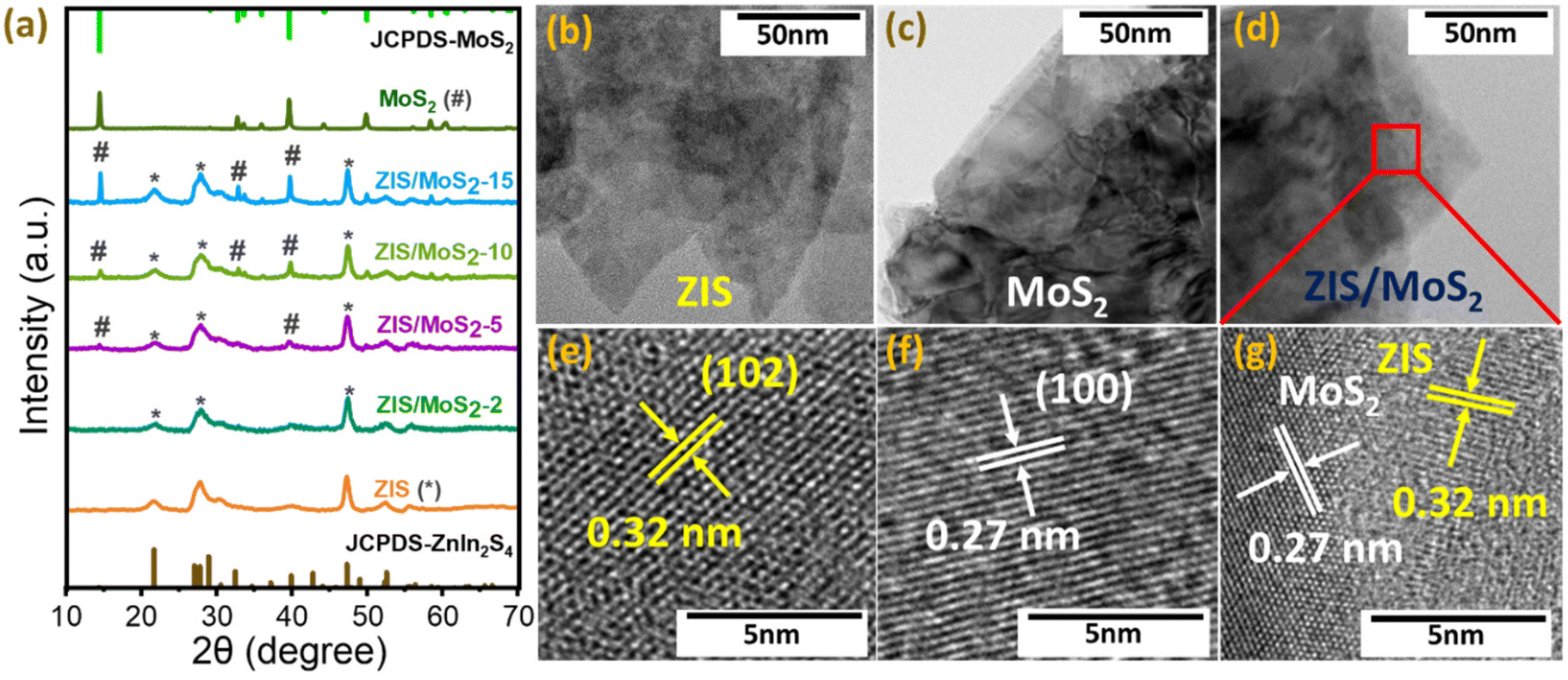 | ||
| Fig. 1 (a) XRD pattern of the as-synthesised ZIS, MoS2, ZIS/MoS2-2, ZIS/MoS2-5, ZIS/MoS2-10 and ZIS/MoS2-15 heterostructures. TEM and HRTEM images of the as-synthesized (b and e) ZIS, (c and f) MoS2, (d and g) the ZIS/MoS2-10 heterostructure. | ||
Next, we studied the surface morphology of the synthesized materials using transmission electron microscopy (TEM) and high-resolution TEM (HR-TEM). Fig. 1b and c show the TEM image of ZIS and MoS2, respectively. Both the pristine systems exhibit a nanosheet-like morphology, as also observed in the field emission scanning electron microscopy (FESEM) images of both the pristine systems (Fig. S1†). As shown in Fig. 1d, the growth of the ZIS nanosheets was observed on top of MoS2 nanosheets in ZIS/MoS2-10, which indicated the formation of the van der Waals heterostructure. Fig. 1(e–g) shows the HR-TEM images of the ZIS, MoS2, and ZIS/MoS2 heterostructure. For ZIS, the interplanar spacing was found to be 0.32 nm, corresponding to the (102) plane of hexagonal ZIS. On the other hand, the HR-TEM image of MoS2 shows the lattice fringes with a d-spacing of 0.27 nm corresponding to the (100) plane observed at a 2θ value of 32.8° in the XRD pattern of MoS2 (Fig. 1a). The HR-TEM image of the ZIS/MoS2 heterostructure (Fig. 1g) disclosed the two different lattice fringes with d-spacing of 0.32 nm and 0.27 nm, corresponding to the (102) and (100) planes of ZIS and MoS2, respectively, which portrays the clear interface between the ZIS and MoS2 nanosheets in the heterostructure.
Furthermore, all the pristine and heterostructures were utilized in the photocatalytic reaction, in which the H2 production was monitored under solar light illumination. Fig. 2a shows the photocatalytic H2 yield for all the synthesized materials. The pristine MoS2 did not show any photocatalytic activity, which was also observed earlier.28,29 The ZIS nanosheets displayed a H2 generation yield of 2276 μmol g−1 under 5 h solar irradiation, resulting in a H2 production rate of 455 μmol g−1 h−1 (Fig. 2b). This H2 production rate increased to 602 μmol g−1 h−1 when 2 wt% of MoS2 was integrated with ZIS nanosheets. The highest evolution rate was measured for the ZIS/MoS2-10 heterostructure as 1280 μmol g−1 h−1, which is nearly 2.8 times higher than that of pristine ZIS. Two other important photocatalytic parameters, solar-to-hydrogen conversion efficiency and apparent quantum efficiency (irradiation wavelength = 400 nm), were also found to be improved in the case of the ZIS/MoS2-10 heterostructure as compared to those of ZIS nanosheets. Detailed calculations are provided in the ESI.† Also, the ZIS/MoS2-10 heterostructure shows better H2 evolution performance in comparison with many previously reported heterostructure-based photocatalysts, as listed in Table S3.† However, further increment of MoS2 (15 wt%) decreased the evolution rate to 813 μmol g−1 h−1; this is possibly due to the suppression of the ZIS active sites after the introduction of excessive MoS2. After that, we also performed the recyclability and stability test for the ZIS/MoS2-10 heterostructure. Fig. S2a† shows the recycling H2 evolution data for the ZIS/MoS2-10 heterostructure. The photocatalyst was found to be stable and retained its H2 evolution performance (92%) after three cycles of 5 h reaction time. The stability of the ZIS/MoS2-10 heterostructure photocatalysts was also illustrated by XRD measurement, which was recorded after the photocatalysis (Fig. S2b†). No significant change was observed in the XRD pattern after the photocatalysis, which further confirmed the photostability of the photocatalyst.
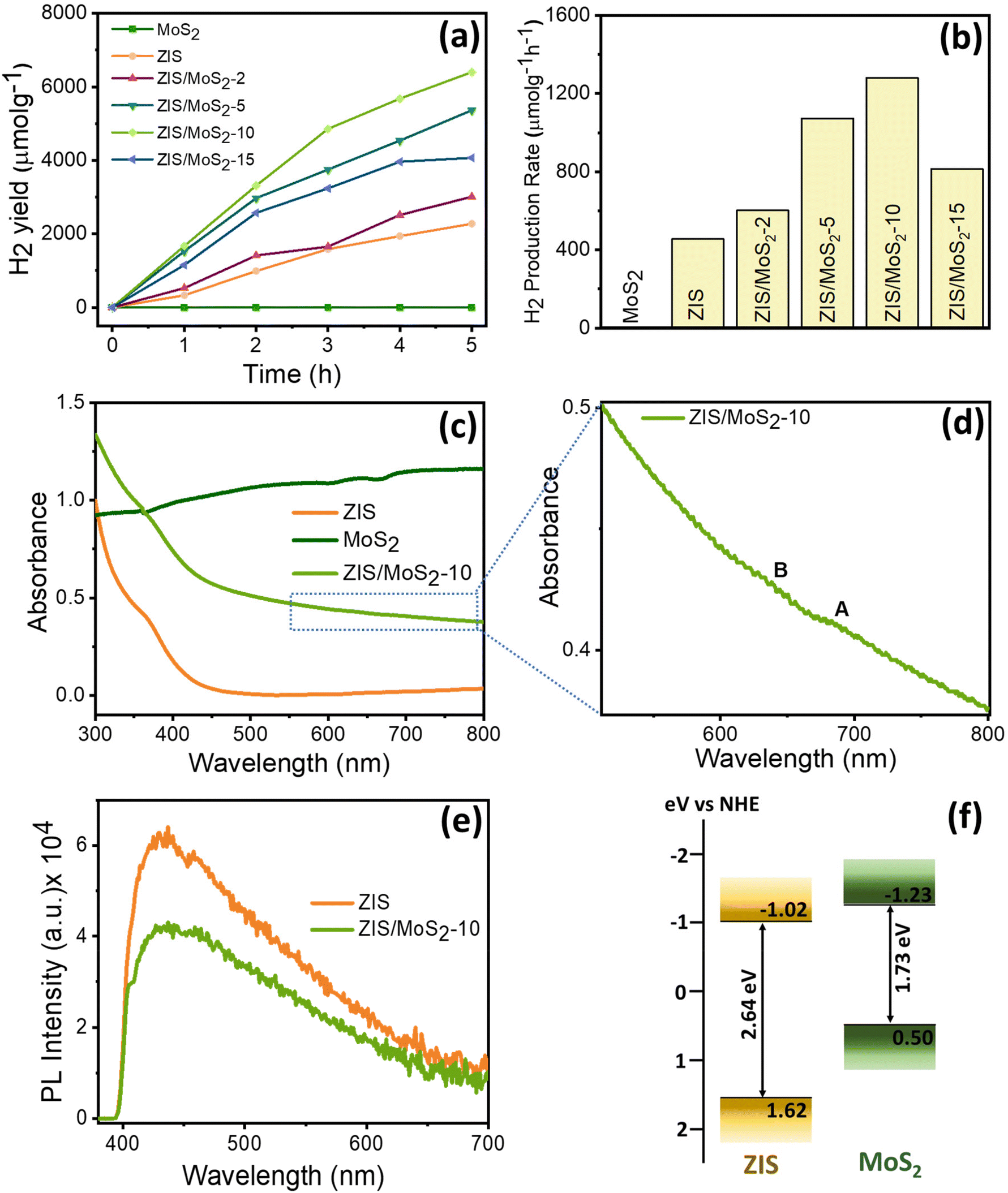 | ||
| Fig. 2 H2 production (a) yields and (b) rates of ZIS, MoS2, ZIS/MoS2-2, ZIS/MoS2-5, ZIS/MoS2-10 and ZIS/MoS2-15 heterostructures. (c) Steady-state absorption spectra of ZIS, MoS2, and ZIS/MoS2-10. (d) Enlarged view for ZIS/MoS2-10. (e) Photoluminescence spectra of ZIS and ZIS/MoS2-10 after photoexcitation at 350 nm. (f) Band position estimation for ZIS and MoS2. | ||
To investigate the reason behind the superior photocatalytic performance of the ZIS/MoS2-10 heterostructure as compared to those of their pristine systems, we conducted an in-depth spectroscopic investigation using a wide range of spectroscopic techniques, including steady-state absorption and photoluminescence (PL) spectroscopy, X-ray photoelectron spectroscopy (XPS) and femtosecond transient absorption (TA) spectroscopy. Fig. 2c displays the steady-state absorption spectra of ZIS, MoS2 and the ZIS/MoS2-10 heterostructure. The ZIS absorption spectra exhibit a peak maximum of around 390 nm, which originates from the higher energy transition.13,26 In the heterostructure, the absorption was observed to be enhanced as compared to that of pristine ZIS due to the presence of MoS2. The characteristic A and B excitonic peaks were also observed in the bare MoS2 flakes and heterostructure, as shown in Fig. 2d. A and B excitons originate from the transition between the conduction band minimum and spin-split valence band maxima at the K point in the momentum space.37,38 The enhanced visible range absorption is beneficial for the heterostructure in photocatalytic hydrogen production. The PL spectra portray the recombination characteristics of charge carriers in the bare ZIS and ZIS/MoS2-10 heterostructure after photoexcitation at 350 nm, as shown in Fig. 2e. The ZIS spectra exhibit a broad PL emission extending beyond 700 nm with a peak maximum of around 435 nm. The 435 nm peak originated from the direct recombination of the conduction band electrons and valence band holes, whereas the extended broad emission in the red region is attributed to the trap state mediated recombination.26 The PL intensity decreased in the heterostructure, which suggests the reduction in the recombination between the CB electrons and VB holes of ZIS, possibly due to the interfacial charge transfer in the heterostructure. The band gaps of ZIS and MoS2 were calculated as 2.64 and 1.73 eV, respectively (Fig. S3b and S3c†), with the help of DRS spectra, whereas the XPS VB spectra determine the respective VB of both semiconductors as 1.62 and 0.50 eV, respectively, as shown in Fig. S3a.† By combining these two pieces of information, the respective band positions were estimated and are shown in Fig. 2f. ZIS and MoS2 show a staggered type band alignment in the heterostructure.
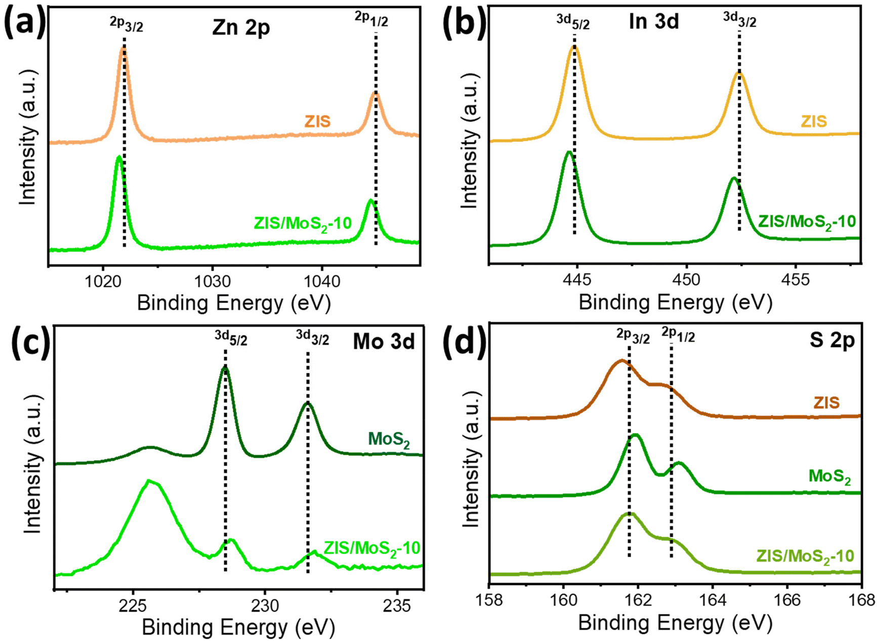
Next, we conducted XPS studies to explore the surface chemical states of the synthesized bare and heterostructures. The high-resolution XPS (HR-XPS) spectra (Fig. 3) confirm the presence of Zn, In, S, and Mo in the pristine and heterostructures. For ZIS, the HR-XPS spectrum of Zn 2p (Fig. 3a) exhibits two peaks at 1021.9 and 1045.0 eV, corresponding to 2p3/2 and 2p1/2, respectively. In Fig. 3b, two peaks at 444.9 and 452.4 eV are attributed to the 3d5/2 and 3d3/2 of In 3d.29 The S 2p spectrum for ZIS (Fig. 3d) showed two characteristic peaks at 161.6 eV (2p3/2) and 162.7 eV (2p1/2),28 whereas for MoS2, S 2p peaks were observed at 162.0 and 163.1 eV. Additionally, two peaks of Mo 3d5/2 and Mo 3d3/2 were found at 228.5 and 231.6 eV, respectively (Fig. 3c), for pristine MoS2.39 It is worth noting that the peaks related to ZIS (Zn 2p, In 3d and S 2p) were observed to be shifted to lower binding energy in the heterostructure. Conversely, Mo 3d of ZIS/MoS2-10 experienced a positive shift to higher binding than pristine MoS2. These outcomes are attributed to the electron migration from MoS2 to ZIS when they are integrated to form a heterostructure, resulting in a generation of the interfacial electric field at the interface with the direction from MoS2 to ZIS. The above results indicate a formation of the S-scheme heterojunction between both nanosheets.20,33
 | ||
| Fig. 3 High-resolution XPS spectra of (a) Zn 2p and (b) In 3d for ZIS and ZIS/MoS2-10 and (c) Mo 3d for MoS2 and ZIS/MoS2-10. (d) S 2p for ZIS, MoS2 and ZIS/MoS2-10. | ||
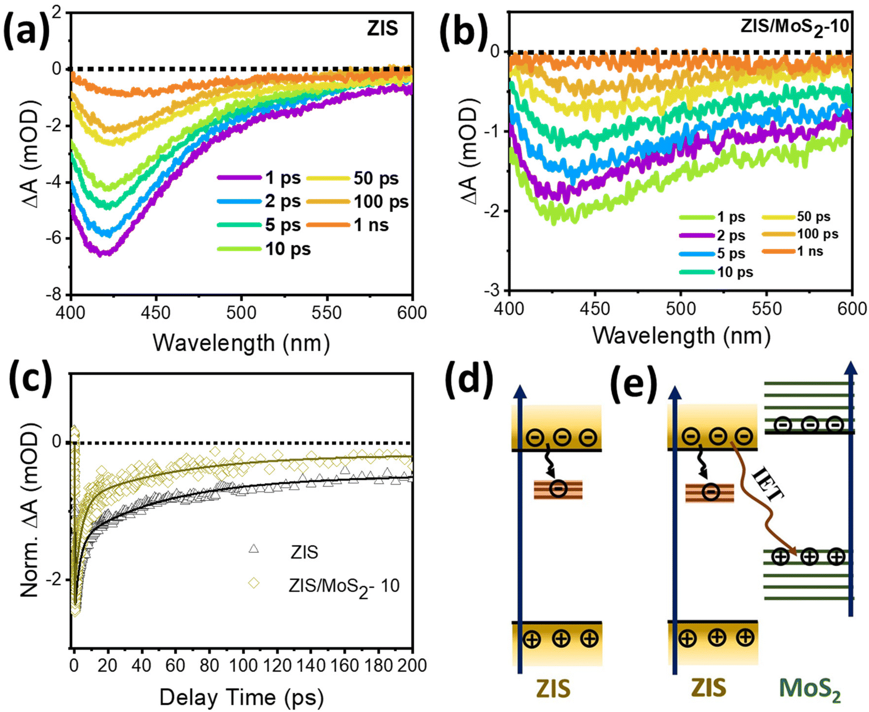
To validate the S-scheme formation and investigate the interfacial photophysical processes involved in the superior photocatalytic performance of the ZIS/MoS2 heterostructure, we employed state-of-the-art Femtosecond TA spectroscopy for pristine nanosheets and their heterostructure. Fig. 4a shows the TA spectra of ZIS as a function of different pump–probe time delays following the photoexcitation at 370 nm. The spectra exhibit a strong photo-induced bleach signal in the spectral range of 400–600 nm, with the peak maxima around 420 nm. In our previous work, we have already assigned this bleach maxima to the transition from the CBM to the VB states.13,26 In addition to a strong bleach maximum, we observed a weak and broad bleach signal in the red region of the spectra, which originated from the mid-band gap trap state transitions.26 The TA kinetics of ZIS, portrayed in Fig. 4c, reflects the time-dependent carrier population at the corresponding state monitored at the bleach maxima (∼420 nm). The TA kinetics was fitted using a multiexponential function with one growth (τg = 0.2 ps) component and three decay components (τ1 = 5.6 ps, τ2 = 52.4 ps and τ3 ≥ 1 ns), which are tabulated in Table S4.† The growth of the bleach signal signifies the time involved in the cooling of the hot carrier to the particular energy state that is being monitored. Meanwhile, the decay time constants correspond to the trapping and recombination processes. The first two decay time constants (τ1 = 5.6 ps and τ2 = 52.4 ps) were assigned to the trapping and de-trapping of the charge carriers in the mid-band gap trap states, respectively (Fig. 4d). The longest-time component (τ3 ≥ 1 ns) is attributed to the electron–hole recombination. The role of individual carriers (electrons and holes) in the relaxation dynamics of the semiconductors is usually determined with the help of electron/hole quenching experiments.33,40 In our study, we used benzoquinone (BQ) and TEOA as electron and hole quenchers, respectively, to find out the contribution of the respective charge carriers in the transient bleach signals of the pristine systems. As shown in Fig. S2a and S2b,† the comparative kinetic profiles monitored at bleach maxima of ZIS validate the domination of electrons in the ZIS bleach signal, as the bleach signal completely quenched around 100 ps with the addition of BQ, whereas the kinetics was observed to be similar in the case of TEOA.
 | ||
| Fig. 4 TA spectra of (a) ZIS nanosheets and (b) the ZIS/MoS2-10 heterostructure after photoexcitation at 370 nm. (c) Comparative TA kinetics of ZIS and ZIS/MoS2-10, monitored at 420 nm. Ultrafast photophysical processes, such as electron trapping and interfacial electron transfer (IET) processes in (d) bare ZIS and (e) the ZIS/MoS2 heterostructure. | ||
Next, we carried out our transient spectroscopic investigation for the ZIS/MoS2-10 heterostructure to understand the interfacial charge transfer phenomena. It is worth mentioning that we maintained similar experimental conditions throughout the TA measurements. The TA spectra of the heterostructure (Fig. 4b), dominated by a broad bleach signal, peaking around ∼423 nm, show a spectral similarity to the pristine ZIS nanosheets. Fig. 4c shows the comparative TA kinetics of ZIS before and after the integration of MoS2 nanosheets. The kinetic profile was observed to be accelerated in the case of ZIS/MoS2-10, with reduced decay time constants (τ1 = 2.7 ps and τ2 = 30.2 ps) as compared to that of pristine ZIS (τ1 = 5.6 ps and τ2 = 52.4 ps), which affirms the interfacial charge transfer from the ZIS to MoS2 side. This charge transfer reduced the charge recombination in the ZIS side as the contribution of the τ3 reduced by half (Table S4†) in the case of the heterostructure (25% for ZIS and 12.5% for ZIS/MoS2-10). As the bleach signal is dominantly contributed by the electrons, the faster TA kinetics can be evidently assigned to the thermodynamically feasible interfacial electron transfer (IET) from the ZIS CB to MoS2 VB, as shown schematically in Fig. 4e. This is an important characteristic evident for the S scheme interface.33,41 In the case of the S-scheme heterojunction, the generated directional electric field from MoS2 to ZIS allows electron migration in the opposite direction, i.e., from ZIS to MoS2 after the light irradiation.19
Furthermore, we conducted TA spectroscopy for another constituent of the heterostructure, i.e., MoS2, in the spectral range of 600–720 nm. Fig. 5a shows the TA spectra of pristine MoS2 nanosheets after 370 nm photoexcitation. The spectrum comprises two bleach signals with maxima positioned at ∼684 nm and ∼620 nm, assigned to the A and B excitonic peaks, respectively. The formation of these excitons in MoS2 is schematically illustrated in Fig. 5d. These excitonic features retained their spectral identity in the case of ZIS/MoS2-10, as portrayed in Fig. 5b. The TA decay kinetics of A excitons for bare MoS2 and the heterostructure (Fig. 5c) were fitted multi-exponentially in three-time constants, as listed in Table S4† (τ1 = 3.02 ps, τ2 = 69.9 ps and τ3 ≥ 1 ns for MoS2, τ1 = 0.94 ps, τ2 = 15.7 ps and τ3 ≥ 1 ns for ZIS/MoS2-10). Faster kinetics was observed for the heterostructure compared to individual MoS2 kinetics, which was expected because of the participation of MoS2 holes in the recombination processes with the interfacial transferred electrons from ZIS (Fig. 5e). The stronger influence of the TEOA (hole quencher) addition as compared to that of BQ (electron quencher) in the kinetic profile of pristine MoS2 (Fig. S4c and S4d†) also supports the above findings, which suggest the recombination of the ZIS CB electrons and MoS2 VB holes due to the IET process. The involvement of the MoS2 holes in the S-scheme recombination process suppressed the recombination on the MoS2 side, as indicated by the reduced proportion of the longest decay component related to charge recombination (τ3 ≥ 1 ns) in the heterostructure (16.7%) as compared to that of pristine MoS2 (33.4%). Consequently, the electrons of the MoS2 CB are isolated, and they actively participate in the photocatalytic H2 reduction process.
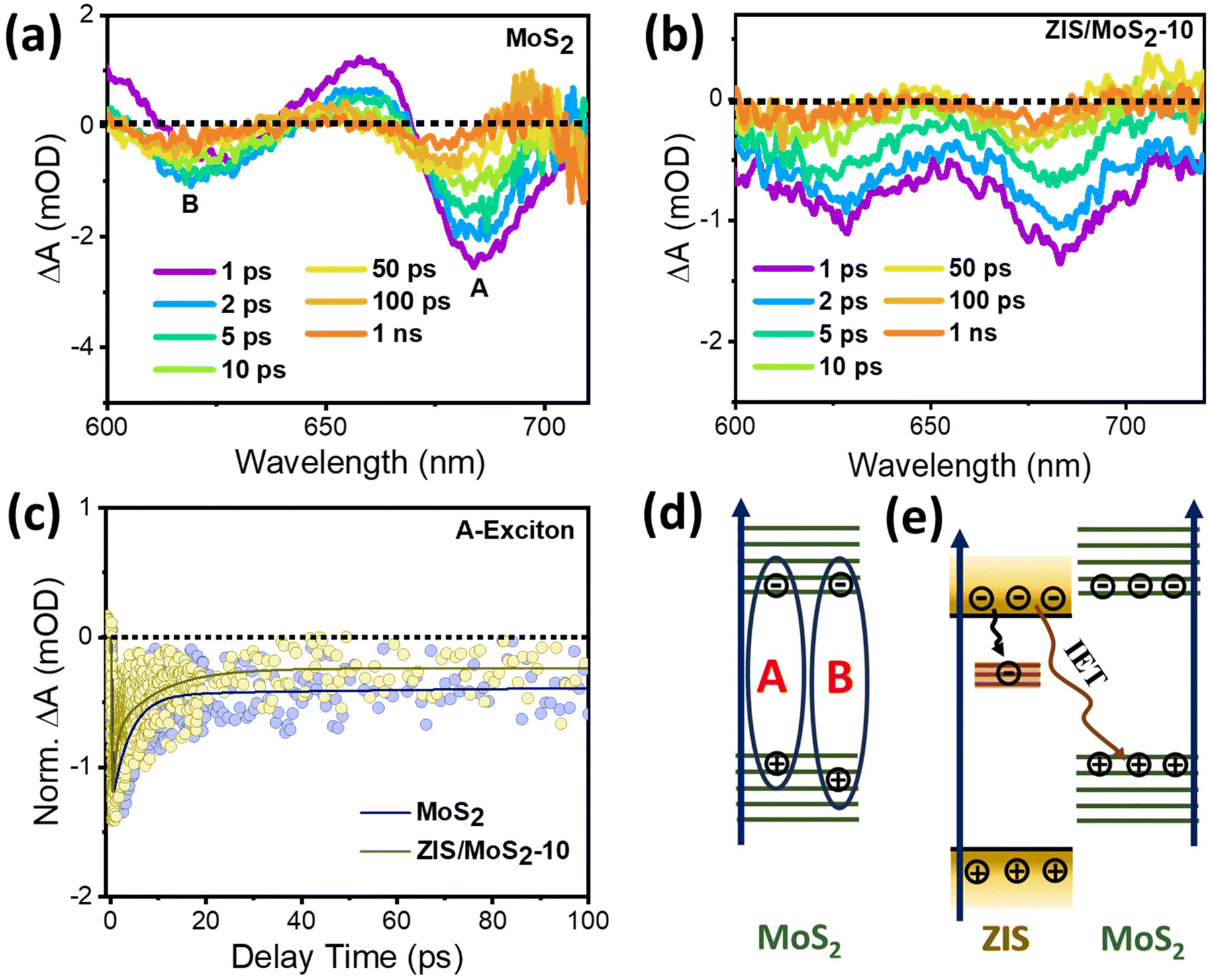 | ||
| Fig. 5 TA spectra of (a) MoS2 and (b) the ZIS/MoS2-10 heterostructure after photoexcitation at 370 nm. (c) Comparative TA kinetics of MoS2 and ZIS/MoS2-10, monitored at the A excitonic position (687 nm). Ultrafast photophysical processes like the formation of A and B excitons and IET in (d) MoS2 and (e) the ZIS/MoS2 heterostructure. | ||
Fig. 6 shows a schematic representation of the proposed photocatalytic H2 production mechanism based on the spectroscopic investigation. In the ZIS/MoS2 heterostructure, the charge carriers (electrons and holes) were generated in both the semiconductors after solar irradiation. Subsequently, the CB electrons of ZIS migrated towards the VB of MoS2 due to the generation of the interfacial electric field in the S-scheme manner (IET) and recombined with the VB holes of MoS2. This interfacial recombination isolated the CB electrons of MoS2 and VB holes of ZIS. The ZIS holes interacted with a sacrificial agent, TEOA. In contrast, the electrons of the MoS2 CB, having a higher reduction potential, efficiently participated in the photocatalytic reduction process and resulted in a higher H2 production for the ZIS/MoS2 heterostructure in comparison with both of its constituents solely.
 | ||
| Fig. 6 Schematic representation of the plausible mechanism of the photocatalytic hydrogen production in the ZIS/MoS2 heterostructure. | ||
Conclusion
In summary, we synthesized a unique S-scheme heterostructure between ZIS and MoS2 using a hydrothermal technique. The TEM measurements confirmed the formation of a van der Waals heterostructure between these two nanosheets. Under solar energy irradiation, the hydrogen evolution rate through photocatalysis in the ZIS/MoS2 heterostructure was quantified at 1280 μmol g−1 h−1, showcasing an increase of almost 2.8 times in comparison with the hydrogen evolution rate of pristine ZIS nanosheets. Steady-state absorption spectroscopy showed enhanced absorption in the visible range for the heterostructure. The lower PL intensity of ZIS/MoS2 is attributed to the lesser recombination in the heterostructure. XPS indicated the creation of a directional electric field from MoS2 to ZIS owing to the S scheme interface characteristics. We further conducted ultrafast TA measurements to investigate the interfacial charge transfer between these two 2D materials. TA study demonstrated the faster decay kinetics for the heterostructure than for both the pristine systems. The quenching experiment revealed the dominance of electrons and holes in the ZIS and MoS2 bleach signals, respectively. TA analysis concluded that the interfacial electron transfer from the conduction band of ZIS to MoS2 enhanced the S-scheme charge separation, which resulted in higher photocatalytic activity in the heterostructure. Overall, this work provides a comprehensive spectroscopic understanding of the interfacial charge carrier dynamics in a 2D/2D ZIS/MoS2 heterostructure. This detailed exploration would be beneficial in designing state-of-the-art van der Waal's heterostructure-based S-scheme photocatalysts and advancing their utilization for industrial H2 production.Data availability
The data supporting this article have been included in the ESI.† It contains synthesis techniques, instrumental details, DRS spectra, XPS valence band spectra, AQE and STH calculations, a performance comparison table, and transient absorption spectra and dynamics.Conflicts of interest
The authors declare no conflicts of interest.Acknowledgements
H. B., M. S. P. and D. K. Y. thank the Institute of Nano Science and Technology (INST), Mohali, India, for providing the research fellowship. T. G. acknowledges the CSIR (09/1129(0009)/2017-EMR-I), India, for providing fellowship during his research tenure. A. S. P. thanks NISER Bhubaneswar for the research fellowship. H. N. G. is grateful to DST, Govt. of India, for the J C Bose Fellowship (JCB/2018/000047) and SERB/DST project (CRG/2019/000938). The authors acknowledge INST, Mohali, India, for providing instrumental facilities and supporting this research work.References
- Z. Yan, K. Yin, M. Xu, N. Fang, W. Yu, Y. Chu and S. Shu, Chem. Eng. J., 2023, 472, 145066 CrossRef CAS.
- B. K. Patra, S. Khilari, D. Pradhan and N. Pradhan, Chem. Mater., 2016, 28, 4358–4366 Search PubMed.
- Y. Liu, W. Yang, Q. Chen, Z. Xie and T. Lian, J. Chem. Phys., 2023, 159, 104706 CrossRef CAS PubMed.
- Y. Magazov, V. Kudryashov, K. Moldabekov, M. Amze, A. Nurmanova, A. Aliyev and N. Nuraje, Commun. Mater., 2024, 5, 126 CrossRef CAS.
- F. Qureshi and M. Tahir, Int. J. Hydrogen Energy, 2024, 69, 760–776 CrossRef CAS.
- X. Chen, W. Pan, R. Guo, X. Hu, Z. Bi and J. Wang, J. Mater. Chem. A, 2022, 10, 7604–7625 RSC.
- M. Zeng, Y. Xiao, J. Liu, K. Yang and L. Fu, Chem. Rev., 2018, 118, 6236–6296 CrossRef CAS PubMed.
- Z. Hu, Z. Wu, C. Han, J. He, Z. Ni and W. Chen, Chem. Soc. Rev., 2018, 47, 3100–3128 RSC.
- R. Yang, Y. Fan, Y. Zhang, L. Mei, R. Zhu, J. Qin, J. Hu, Z. Chen, Y. Hau Ng, D. Voiry, S. Li, Q. Lu, Q. Wang, J. C. Yu and Z. Zeng, Angew. Chem., Int. Ed., 2023, 62, e202218016 CrossRef CAS PubMed.
- Q. H. Wang, K. Kalantar-Zadeh, A. Kis, J. N. Coleman and M. S. Strano, Nat. Nanotechnol., 2012, 7, 699–712 CrossRef CAS PubMed.
- D. Monga, S. Sharma, N. P. Shetti, S. Basu, K. R. Reddy and T. M. Aminabhavi, Mater. Today Chem., 2021, 19, 100399 CrossRef CAS.
- S. Saeed, E. M. L. D. de Jong, K. Dohnalova and T. Gregorkiewicz, Nat. Commun., 2014, 5, 4665 CrossRef CAS PubMed.
- H. Bhatt, T. Goswami, D. K. Yadav, N. Ghorai, A. Shukla, G. Kaur, A. Kaur and H. N. Ghosh, J. Phys. Chem. Lett., 2021, 12, 11865–11872 CrossRef CAS PubMed.
- B. Zhu, J. Sun, Y. Zhao, L. Zhang and J. Yu, Adv. Mater., 2024, 36, 2310600 CrossRef CAS PubMed.
- L. Zhang, J. Zhang, H. Yu and J. Yu, Adv. Mater., 2022, 34, 2107668 CrossRef CAS PubMed.
- J. Wang, R. Pan, S. Yan, R. Wang, X. Niu, Q. Hao, J. Ye, Y. Wu and H. Ying Yang, Chem. Eng. J., 2023, 463, 142489 CrossRef CAS.
- H. Tran Huu, M. D. N. Thi, V. P. Nguyen, L. N. Thi, T. T. T. Phan, Q. D. Hoang, H. H. Luc, S. J. Kim and V. Vo, Sci. Rep., 2021, 11, 14787 CrossRef CAS PubMed.
- A. Xu, Y. Zhang, H. Fan, X. Liu, F. Wang, X. Qu, L. Yang, X. Li, J. Cao and M. Wei, ACS Appl. Nano Mater., 2024, 7, 3488–3498 CrossRef CAS.
- X. Luan, Z. Yu, J. Zi, F. Gao and Z. Lian, Adv. Funct. Mater., 2023, 33, 2304259 CrossRef CAS.
- X. Hu, Y. Xu, S. Tang, W. Shi, X. Wang, Y.-X. Yu and W.-D. Zhang, Small, 2024, 20, 2306563 CrossRef CAS PubMed.
- F. Zhao, X. Yao, Y. Zhao, J. Yu, J. Dong, X. Liu, J. Cao, D. Zhang and X. Pu, J. Colloid Interface Sci., 2024, 675, 471–480 CrossRef CAS PubMed.
- Q. Liu, X. Yao, X. Zhao, F. Zhang, D. Zhang, J. Liu, P. Cai and X. Pu, Surf. Interfaces, 2024, 54, 105213 CrossRef CAS.
- N. Li, J. Ma, W. Wang, Q. Chang, L. Liu, C. Hao, H. Zhang, H. Zhang, S. Hu and S. Wang, J. Colloid Interface Sci., 2024, 676, 496–505 CrossRef CAS PubMed.
- D. Zhang, D. Zhang, F. Zhao, Y. Zhao, H. Li, J. Liu, X.-Y. Ji, X. Pu and H. Zhang, J. Mater. Chem. A, 2024, 12, 33546–33558 RSC.
- W.-K. Chong, B.-J. Ng, Y. J. Lee, L.-L. Tan, L. K. Putri, J. Low, A. R. Mohamed and S.-P. Chai, Nat. Commun., 2023, 14, 7676 CrossRef CAS PubMed.
- T. Goswami, D. K. Yadav, H. Bhatt, G. Kaur, A. Shukla, K. J. Babu and H. N. Ghosh, J. Phys. Chem. Lett., 2021, 12, 5000–5008 CrossRef CAS PubMed.
- Z. Li, X. Meng and Z. Zhang, J. Photochem. Photobiol., C, 2018, 35, 39–55 CrossRef CAS.
- Z. Zhang, L. Huang, J. Zhang, F. Wang, Y. Xie, X. Shang, Y. Gu, H. Zhao and X. Wang, Appl. Catal., B, 2018, 233, 112–119 CrossRef CAS.
- W. Li, Z. Lin and G. Yang, Nanoscale, 2017, 9, 18290–18298 RSC.
- K. L. Corp and C. W. Schlenker, J. Am. Chem. Soc., 2017, 139, 7904–7912 CrossRef CAS PubMed.
- T. Goswami, H. Bhatt, D. K. Yadav and H. N. Ghosh, J. Phys. Chem. B, 2022, 126, 572–580 CrossRef CAS PubMed.
- C. Feng, T. Bo, P. Maity, S. Zuo, W. Zhou, K.-W. Huang, O. F. Mohammed and H. Zhang, Adv. Funct. Mater., 2024, 34, 2309761 CrossRef CAS.
- X. Deng, J. Zhang, K. Qi, G. Liang, F. Xu and J. Yu, Nat. Commun., 2024, 15, 4807 CrossRef CAS PubMed.
- R. Li, H. Li, X. Zhang, B. Liu, B. Wu, B. Zhu, J. Yu, G. Liu, L. Zheng and Q. Zeng, Adv. Funct. Mater., 2024, 34, 2402797 CrossRef CAS.
- T. Goswami, H. Bhatt, D. K. Yadav, R. Saha, K. J. Babu and H. N. Ghosh, J. Chem. Phys., 2022, 156, 034704 CrossRef CAS PubMed.
- A. Kaushik, J. Singh, R. Soni and J. P. Singh, ACS Appl. Nano Mater., 2023, 6, 9236–9246 CrossRef CAS.
- L. Wang, Z. Wang, H.-Y. Wang, G. Grinblat, Y.-L. Huang, D. Wang, X.-H. Ye, X.-B. Li, Q. Bao, A.-S. Wee, S. A. Maier, Q.-D. Chen, M.-L. Zhong, C.-W. Qiu and H.-B. Sun, Nat. Commun., 2017, 8, 13906 CrossRef CAS PubMed.
- T. Goswami, H. Bhatt, K. J. Babu, G. Kaur, N. Ghorai and H. N. Ghosh, J. Phys. Chem. Lett., 2021, 12, 6526–6534 CrossRef CAS PubMed.
- W. Yan, Y. Xu, S. Hao, Z. He, L. Wang, Q. Wei, J. Xu and H. Tang, Inorg. Chem., 2022, 61, 4725–4734 CrossRef CAS PubMed.
- S. Kaniyankandy, S. N. Achary, S. Rawalekar and H. N. Ghosh, J. Phys. Chem. C, 2011, 115, 19110–19116 CrossRef CAS.
- M. Zhu, Z. Sun, M. Fujitsuka and T. Majima, Angew. Chem., Int. Ed., 2018, 57, 2160–2164 CrossRef CAS PubMed.
Footnote |
| † Electronic supplementary information (ESI) available. See DOI: https://doi.org/10.1039/d4nr05043f |
| This journal is © The Royal Society of Chemistry 2025 |