
 Open Access Article
 This Open Access Article is licensed under a Creative Commons Attribution-Non Commercial 3.0 Unported Licence
Flexible Cu(In,Ga)Se2 photovoltaics for bending applications: advances from materials to panels
Ha Kyung
Park
 and
William
Jo
*
and
William
Jo
*
Department of Physics, Ewha Womans University, Seoul, Republic of Korea. E-mail: wmjo@ewha.ac.kr
First published on 27th December 2024
Abstract
Recent efforts to achieve effective and sustainable power generation in urban environments have increasingly focused on flexible thin-film photovoltaics, owing to their versatile applications in building-integrated and mobile devices. However, addressing this challenge requires a deeper understanding of bending-induced properties and the development of sustainable device structures. Decades of extensive research on chalcopyrite [Cu(In,Ga)Se2 (CIGS)]-based photovoltaics have led to substantial advances in the development of highly reliable and efficient solar energy generation systems. Furthermore, improvements in the well-controlled and scalable manufacturing processes of flexible CIGS solar cells have brought them closer to commercialization. This review discusses key strategies for substrate selection, artificial doping, and module fabrication, focusing on the progress achieved in the transition from laboratory research to practical commercial applications. Additionally, the review provides a detailed explanation of the evaluation methods for mechanical flexibility and durability, as well as an investigation into bending-induced phenomena. The review also examines future perspectives in the development of tandem solar cells incorporating flexible frameworks.
1. Introduction
The increasing demand for effective and sustainable power generation solutions has driven the development of flexible photovoltaics with versatile applications and high throughput capabilities. Through decades of extensive research, chalcopyrite Cu(In,Ga)Se2 (CIGS) solar cells have now achieved a record efficiency of over 23%.1,2 Furthermore, recent advancements in the fabrication of flexible photovoltaic devices have increased their efficiencies to over 22%, nearly matching that of their rigid counterparts.3 Notably, the high stability and durability of CIGS solar cells, even under harsh environmental conditions, render them suitable for use in various demanding applications, including outdoor use, space missions, and portable energy applications. While the traditional Si solar panels available commercially exhibit excellent performances, flexible CIGS thin-film solar cells provide the additional advantage of being lightweight, resulting in a high power-to-weight ratio. Furthermore, the availability of a well-controlled and scalable manufacturing process for CIGS thin-film solar cells facilitates their commercialization.This review covers recent progress in the fabrication of highly efficient and reliable flexible CIGS solar cells and outlines their future prospects in advanced applications. The review begins by introducing the technologies specific to flexible CIGS solar cells, including various flexible substrates and materials for buffers and electrodes. This review also discusses manufacturing techniques for producing large-area modules and outlines the current industrial status. The flexibility of the CIGS solar cells is thoroughly discussed, along with performance evaluations based on bending tests. Bending-induced phenomena at both micro- and macroscopic scales are discussed, and the recently reported piezo-phototronic effect under mechanical stress conditions is reviewed. Finally, future outlooks are discussed, focusing on advanced applications such as bifacial and tandem solar cells.
2. Rigid and flexible CIGS thin-film solar cells
Chalcopyrite CIGS is a p-type compound well-suited as a light absorber, owing to its direct band transition and high absorption coefficient of approximately 10−5 cm−1.4,5 In particular, the bandgap of CIGS can be tuned within the range of 1.04 eV (CuInSe2) to 1.68 eV (CuGaSe2) by varying the ratio of In and Ga.4 Additionally, the high absorption efficiency of CIGS materials allows for a thin light-absorbing layer of 1–2 μm. Following several decades of research, most CIGS solar cells utilize a substrate configuration, as shown in Fig. 1a. In this structure, light entering through the transparent conductive oxide (TCO) window transmits the n-type buffer, while a built-in electric field at the CIGS/CdS pn junction drives electrons from the p-type absorber to the n-type buffer.6 Both vacuum and non-vacuum processes have been developed for fabricating the CIGS absorber layer, with the three-stage co-evaporation process being the most widely used technique, well-suited for roll-to-roll mass production.7 For the buffer layer, CdS deposited using chemical bath deposition methods has traditionally been used, while Cd-free buffers have also been developed through vacuum-based processes.7 | ||
| Fig. 1 (a) The substrate structure of CIGS solar cells, showcasing representative materials for each layer and their optimal thickness. (b) The efficiency progress of polyimide-based flexible CIGS solar cells, emphasizing key advancements. | ||
Conventional CIGS solar cells use soda-lime glass (SLG), which can introduce alkali elements improving the quality of CIGS thin films. However, it has the drawback of being significantly heavier than most flexible substrate candidates. For instance, the weight of ceramic-based flexible CIGS solar modules is only one-tenth that of conventional rigid photovoltaic modules, which typically range from 10 to 20 kg m−2.8 Namely, lightweight substrates offer a higher specific power output (kW kg−1), improving efficiency and portability compared to fragile glass substrates.9 Additionally, the biggest advantage of flexible substrates is their compatibility with roll-to-roll processes for scalable coating, which reduces production costs by enabling high throughput and minimizing material consumption.10
In 1974, CuInSe2/CdS heterojunction solar cells were first reported by Bell Laboratory,11 and subsequently, the CIGS composition with added Ga was explored.12 After the co-evaporation method enabling Ga gradient was reported, it became the most widely used technique.13 The efficiency improved with the incorporation of alkali Na elements and a thin CdS buffer,14 exceeding 20%, particularly with the use of heavy alkali elements (K, Rb, and Cs).15,16 In 2019, a 23.35% efficiency was achieved with a Cd-free Zn(O,S,OH)x/Zn0.8Mg0.2O double-buffer layer,2 and after five years, high-concentration Ag alloying recently pushed it to 23.6%, the highest efficiency reported to date.1
The efficiency improvement trends of flexible CIGS solar cells have adopted strategies similar to those used for rigid counterparts. For instance, Fig. 1b illustrates the efficiency progress of polyimide (PI)-based flexible CIGS solar cells, highlighting key advancements. In 1996, the first PI-based flexible CIGS solar cell was reported,17 and device performance was subsequently optimized through controlled Na doping.18–22 Additionally, a sharp performance improvement was achieved through precise control of the composition gradient in the CIGS absorber layer.23–25 Notably, efficiencies exceeding 20% were achieved with heavy alkali doping.26,27 More recently, the highest efficiency of 22.2%, the best among all flexible CIGS solar cells, was attained through the combined optimization of composition and alkali treatments.3
Flexible CIGS solar cells have been elevated to a performance level comparable to rigid cells, enabling their commercialization. As shown in Table 1, flexible CIGS thin-film solar panels available on the market present higher bendability (up to 360°) than their flexible monocrystalline Si counterparts, which have a bendability of 30° to 240°. (Windy Nation Inc. developed 360°-bendable monocrystalline solar panels.28) The high flexibility of flexible CIGS solar panels reduces both shipping costs (through rolled shipment of lightweight panels) and storage space (through compact rolled storage). Building on the advantages of flexible CIGS solar cells, namely their remarkable flexibility and lightweight design, these modules are widely used in applications such as transportation, carports, roofs, and energy harvesting in off grid environments.29,30 Additionally, flexible CIGS solar modules are half as thick as flexible monocrystalline silicon panels, both manufactured by Renogy.31,32 A previous study demonstrated the practical operation of flexible CIGS solar panels from Miasolé in a building-integrated photovoltaic system, highlighting efficient energy generation as well as the limitations related to installation angle dependence.33
| Company | Miasolé | BougeRV | Renogy | |
|---|---|---|---|---|
| Model | FLEX-03 W 1.0 m | Yuma 200 W CIGS (with tape) | Renogy 150 W CIGS solar panel | Flexible monocrystalline solar panel |
| Power (W) | 200 | 100 ± 5% | 150 | 100 ± 3% |
| Efficiency (%) | 18.3 | 17 | 14 | 15.70 |
| Open circuit voltage (V) | 29.2 | 30.5 ± 5% | 23.75 | 24.4 |
| Dimensions (mm) | 1010 × 1292 × 2.5 | 2089 × 660 × 1.52 | 1658 × 646 × 1.5 | 1093 × 582 × 3 |
| Thickness (mm) | 2.5 | 1.52 | 1.5 | 3 |
| Weight | 5.7 lb/2.6 kg | 8.4 lb/3.8 kg | 6.6 lb/3.0 kg | 5.3 lb/2.4 kg |
| Operating temperature (°C) | −40 to 85 | −40 to 85 | −40 to 85 | −40 to 85 |
| Bendability (°) | 360 | 360 | 360 | 240 |
| Ref. | 29 | 30 | 31 | 32 |
3. Selection of flexible materials
3.1 Flexible substrates
Various flexible substrates, such as metal foils, steels, and polymer films, have been proposed for use in flexible CIGS thin-film solar cells. The performance of flexible CIGS solar cells with various substrates is summarized in Table 2. Generally, these substrates are required to possess high flexibility in order to be suitable for large-scale production processes, such as roll-to-roll techniques.7 Furthermore, low-cost and sustainable materials are the preferred choice to enhance both commercial viability and environmental impact. To withstand the vacuum and chemical deposition processes involved in the fabrication of CIGS solar cells, the substrates must also have high chemical inertness, mechanical robustness, vacuum compatibility, and thermal stability. The surface roughness is another critical factor, as a smoother surface facilitates the deposition of Mo and CIGS layers with strong adhesion, minimizing the formation of interfacial voids.34 Furthermore, to reduce thermal stress, the coefficient of thermal expansion (CTE) of the substrate material must closely match that of the deposited layers.35Table 3 provides the CTE values for substrate and solar cell materials, along with the maximum substrate temperatures required to prevent deformation.| Substrate | Efficiency (%) | Year | Author/institute | Ref. | |
|---|---|---|---|---|---|
| Metal foils | Mo foil | 14.6 | 2010 | AIST | 36 |
| Ti foil | 17.9 | 2009 | T. Yagioka | 37 | |
| Al foil | 17.1 | 2011 | Nanosolar | 38 | |
| Cu foil | 9.91 | 2018 | J.-K. Sim | 39 | |
| Kovar | 10.6 | 2003 | K. Herz | 40 | |
| SS | 18.1 | 2023 | J. Chantana | 41 | |
| Polymer foils | PI | 20.4 | 2013 | A. Chirila | 26 |
| PTFE* | 6.6 | 2010 | T. Minemoto | 42 | |
| ETFE* | 12.8 | 2020 | N. Hamada | 43 | |
| FEP* | 11.5 | 2020 | T. Nishimura | 44 | |
| PET | 4.21 | 2011 | M. Faraj | 45 | |
| Polyamide | 13.1 | 2018 | A. Illiberi | 46 | |
| UTG | 13.23 | 2020 | D. Kim | 47 | |
| Zirconia ceramic | 18.65 | 2022 | S. Ishizuka | 8 | |
| Paper* | 5.48 | 2016 | K.-C. Tseng | 48 | |
| Materials | CTE (10−6 K−1) | Maximum Ts (°C) |
|---|---|---|
| a The temperature at which unsupported material starts to deform. | ||
| Substrates | ||
| SLG | 9 (20–300 °C) | ∼600 |
| UTG | 7.2 | ∼736a |
| Al | 22.2 | ∼600 |
| Ti | 8.6 | >600 |
| Cu | 16.6 | >600 |
| Mo | 5.4 | >600 |
| SS (SS430) | 10–11 | >600 |
| PI (Upilex S) | 12–24 | ∼450 |
| PET | 60 | ∼500 |
| ZrO2 | 5.7 | >600 |
| Solar cell layers | ||
| CIGS | 7.9–11.4 | |
| CdS | 4.5 | |
| ZnO | 3–5 | |
Metal foils, which are highly heat resistant and lightweight, were among the first candidates considered for the production of flexible substrates. Mo foils, in particular, are advantageous as they can serve as both substrate and back contact. In 2010, a research group at the National Institute of Advanced Industrial Science and Technology (AIST) achieved an efficiency of 14.6% using a Mo foil-based device.36 However, further advances in the development of Mo foil-based devices have been limited, likely owing to their higher costs compared to other metals or steel materials. Among the metal foil-based devices developed to date, the Ti foil-based devices have shown the best performance, reaching an efficiency of 17.9%, particularly when equipped with a Cd-free ZnS(O,OH) buffer layer.37 However, other metal foils such as Cu and Al present challenges associated with their high CTEs (16.6 × 10⁻⁶ and 22.2 × 10⁻⁶ K−1, respectively), which can lead to the development of substantial residual stresses after high-temperature processing. A previous study attempted to use Ni foil as a substrate, owing to its lower surface roughness compared to Ti foils.50 However, CIGS films deposited on the Ni foil exhibited lower compactness and grain sizes, along with the formation of detrimental In–Ni and Ga–Ni alloys. Furthermore, unlike SLG, metal foils lack alkali elements that can exert positive impacts such as improving the grain growth, thereby requiring additional alkali doping to maximize the performance.
Stainless steel (SS) is another commonly used flexible substrate for CIGS solar cells, largely owing to its high thermal stability and relatively low cost. Being available in the market, SS is frequently employed for fabricating flexible CIGS solar panels for commercial use. Among various formulations, Cr-free SS is cheaper but less resistant to corrosion compared to the Cr-containing SS. In the corrosion-resistant Cr-containing SS series (300 and 400 series), the CTE of the 400 series better aligns with that of CIGS films (11 × 10−6 K−1 for SS430).51 Furthermore, the 400 series is relatively cheaper than the 300 series owing to the lack of Ni. Recently, significant progress has been made in improving the efficiency of SS-based devices. For instance, in 2023, Chantana et al. achieved a new record efficiency of 18.1% for SS-based devices by optimizing the band alignment at the interface using a double buffer layer.41 This optimization improved the conduction band offsets (CBOs) at the absorber/buffer and absorber/TCO layer interfaces, suppressing the carrier recombination and enhancing the device performance. Mild steel (MS) is another candidate substrate, with lower cost and high corrosion resistance compared to SS. In 2011, a device using MS as substrate was reported to achieve an efficiency of 18.2% by incorporating a thin enamel layer.38 Notably, such enamel layers introduced on low-carbon steel not only serve as diffusion layers, but also function as alkali (Na and K) sources.52 Interestingly, these enameled steel materials have been demonstrated to be suitable for creating monolithic interconnections, as they can form insulation layers, achieving a module efficiency of 15% for 10 cells occupying an area of 48.0 cm2. Furthermore, Zortea et al., from the Swiss Federal Laboratories for Materials Science and Technology (EMPA), reported an efficiency of 18% for a device fabricated using Ni/Cr-coated MS substrates doped with heavy alkali elements (Rb).53
However, the use of SS and MS substrates presents challenges due to the diffusion of impurities, particularly Fe and Cr, during the fabrication process.54 High concentrations of these diffused impurities, particularly Fe, are detrimental as they form deep defect states in the CIGS layer, reducing the carrier lifetime.55 To mitigate this issue, various diffusion barrier layers, such as metals (Cr,56 Fe57), nitrides [AlN,58 Ti (TiN)59], and oxides (SiO2,60–63 Al2O364) are employed to block the diffusion of impurities. In addition to preventing impurity diffusion, these barriers must provide a smooth, pinhole-free surface to ensure strong adhesion. Furthermore, these barriers act as insulating layers between the metal substrate and monolithically interconnected cells, thus requiring high resistance and an optimal thickness. A simulation study showed that, while a thicker diffusion barrier can reduce residual stress, a thinner barrier is more effective at preventing the delamination of the CIGS layer from the Mo layer.65 However, the addition of barrier layers increases both the production time and cost.
Polymers are widely employed for monolithic integration into CIGS solar cells, owing to their insulating properties and lightweight characteristics, which help reduce mass production costs related to shipping and packaging. Unlike metal films, polymer films do not introduce metallic impurities that can diffuse into the CIGS layer, circumventing the need for a diffusion barrier. Furthermore, some polymers such as PI exhibit a lower CTE (12 × 10−6 K−1)66 than metal foils, which helps to reduce intrinsic stresses originating from CTE mismatches. However, polymer films generally have lower heat resistance than metal foils, and can thus deform at high temperatures. For instance, PI can withstand temperatures of up to 450 °C; hence, the processing temperature must be maintained below this limit to avoid substrate deformation. Despite this limitation, the highest efficiency of flexible CIGS solar cells has been achieved using a PI substrate.26
Other polymer films such as polytetrafluoroethylene (PTFE),42 ethylene tetrafluoroethylene (ETFE),43 and fluorinated ethylene propylene (FEP)44 films have also been investigated as alternative substrates, particularly for transferring and attaching CIGS cells through lift-off processes. While these polymer films exhibit high transparency and durability, their low thermal tolerance (approximately 260 °C for PTFE42 and 200 °C for FEP) prevents the direct deposition of CIGS absorber layers.
In addition to metals and polymers, several other flexible materials have also been investigated for use in CIGS solar cells. For instance, in 2008, the Ishizuka group at the AIST reported that flexible CIGS solar cells deposited on zirconia ceramic substrates achieved an efficiency of 17.7% in the early stages of development.67 These substrates also exhibited lower surface roughness compared to Ti foils, prompting their application in monolithic modules. Ultimately, optimizing the alkali doping enabled the development of monolithically integrated submodules using zirconia ceramic substrates, exhibiting an efficiency of 15.9% for an aperture area of 75.7 cm2.68 Further improvements, such as the incorporation of heavy alkali elements, increased the efficiency of zirconia-based CIGS solar modules to 18.65%.8 However, its brittle nature makes it unsuitable for roll-to-roll manufacturing.9 Paper substrates represent another promising option, owing to their unparalleled eco-friendliness and biodegradability compared to other flexible materials. Furthermore, these substrates are extremely cost-effective, lightweight, and easy to recycle, which helps reduce production and disposal costs. Voggu et al. used bacterial cellulose paper as a substrate for solar cells based on spray-coated CuInSe2 nanocrystals.69 These devices showed high flexibility and robustness during mechanical bending tests with an indium tin oxide (ITO) top electrode layer. Furthermore, the successful transfer of CIGS devices to paper substrates using a lift-off process has also been reported.48
3.2 Flexible materials for electrodes
Enhancing the flexibility of all layers (not only the substrate) is essential for developing flexible and robust CIGS thin-film solar cells suitable for non-flat surfaces. ITO or aluminum-doped zinc oxide (AZO) are extensively used for TCO window layers, owing to their high optical transmittance and low resistivity.70 However, their inherent brittleness and fragility limit the flexibility of the resulting solar cells, as these materials are prone to cracking or delamination under repeated bending cycles, which can degrade the panel performance. Furthermore, the wide grid patterns can block sunlight, reducing the active area available for absorption; hence, these grid areas need to be minimized. Interestingly, the incorporation of metal nanowires (NWs) can potentially minimize the grid area and simultaneously enhance the flexibility of the device.71 However, the inclusion of metal NWs into flexible devices has rarely been reported. For instance, Tsai et al. employed AZO/Ag-NW/AZO sandwich-structured electrodes, which effectively improved the charge carrier collection and extraction.72 Devices assembled with such Ag-NW sandwich-structured electrodes exhibited remarkable durability, retaining approximately 95% of their initial performance even after 1000 bending cycles. Meanwhile, other conventional devices with ITO or AZO layers only maintained approximately 57% of their initial performance. However, the overall efficiency of devices with the Ag-NW electrodes remained relatively low (6.04%). Recently, Cho et al. developed a scalable and facile electroplating method to produce metal microfibers (MFs), which could achieve high performances by carefully controlling the processing time.73 As illustrated in Fig. 2a, Ni and Cu MFs were created on a metal frame using an electroplating method and subsequently transferred onto a solar cell. These MFs proved suitable for series connections in solar cells without leading to significant performance losses, owing to their high conductivity and transparency (Fig. 2b). Furthermore, a research group at the EMPA explored the use of Ag meshes, observing an improvement in charge carrier extraction in the long-wavelength range, particularly when paired with an optimally thick TCO layer (Fig. 2c).74 To further enhance the performance, Kim et al. proposed a method to minimize optical reflection losses at metal grids by designing a microprism array on soft polydimethylsiloxane.75 Notably, this array refracted normally incident light into active areas not covered by metal grids, thereby enhancing the light absorption and increasing the photocurrent. Although metal mesh grids or NWs cannot serve as standalone electrodes without additional TCO layers, they substantially improve the mechanical durability of flexible devices, suggesting their potential for broader application in flexible CIGS solar cells. | ||
| Fig. 2 (a) Schematic illustration showing the fabrication and transfer of metal microfibers onto flexible CIGS solar cells. (b) Ni microfibers subjected to electroplating durations (tEP) of 20, 40, and 60 s. ((a) and (b) Reproduced from ref. 73 with permission from Elsevier, Copyright 2024) (c) scanning electron microscopy (SEM) images of Ag mesh grids on PET substrates before and after flash lamp annealing. (Reproduced from ref. 74 with permission from Taylor & Francis, Copyright 2018). | ||
4. Materials engineering
4.1 Fabrication and engineering of CIGS thin films
Although the manufacturing process for rigid CIGS solar cells is well established, the high temperatures required for CIGS growth limit its deposition on flexible materials with low heat resistance. This temperature constraint also affects the cost competitiveness of the resulting flexible solar cells. As illustrated in Fig. 3a, introducing Ag during grain growth is among the most common synthesis strategies facilitating low-temperature processing. Although few studies have applied Ag alloying in flexible CIGS solar cells, a thin Ag layer is commonly deposited either before or during CIGS growth to introduce Ag into the CIGS thin film.76,77 A previous study demonstrated a unique hybrid sputtering–evaporation method using rotating transfer cylinders, which could be employed in industrial applications. However, this method requires both sputtering and evaporation steps, which increase the process time (Fig. 3b).78 To further reduce production costs, a previous study employed the pulsed electrodeposition technique to synthesize a CIGS thin film, which exhibited an efficiency of 3.9%.79 Despite this low efficiency, the pulsed electrodeposition technique holds promise as an industrially viable and cost-effective production process. The sequential deposition of metallic precursors provides an alternative to co-evaporation; however, it also requires high-temperature selenization.80 Another study applied the non-vacuum aqueous spray deposition method to a flexible SS substrate. Although this method could reduce production costs, it requires a high-temperature selenization process to achieve the desired properties (Fig. 3c).81 Compared to vacuum-based processes, non-vacuum solution-based deposition techniques are cost-effective as they do not require expensive facilities and consume less power. Furthermore, an alternative non-vacuum strategy involves using the ink-printing method, which is suitable for cost-effective large-scale production within a short time frame.82 However, solution-based CIGS solar cells have demonstrated lower efficiencies, with a record efficiency of 17.3%, approximately 30% lower than that of vacuum-based cells.83 Additionally, most solution precursors rely on toxic and environmentally hazardous solvents, such as hydrazine and hydrochloric acid, which may leave impurities like carbon and chlorine. While thiol–amine mixture solvents have been proposed as a safer alternative to flammable and carcinogenic hydrazine, some thiols remain toxic, and challenges persist in achieving compactness and stoichiometric control for thick layer growth.84 | ||
| Fig. 3 (a) Structure of flexible solar cell with an Ag-alloyed CIGS absorber layer. (Reproduced from ref. 76 with permission from Springer Nature, Copyright 2023) (b) schematic illustration of hybrid sputtering–evaporation method. (Reproduced from ref. 78 with permission from Elsevier, Copyright 2018) (c) schematic illustration of aqueous spray deposition and selenization processes. (Reproduced from ref. 81 with permission from Elsevier, Copyright 2022). | ||
Similar to rigid CIGS solar cells, the effects of Ga grading in the absorber layer and the optimal value of the [Ga]/([Ga] + [In]) (GGI) ratio have been thoroughly investigated in SS-85,86 and PI-based devices.87 Optimal Ga grading enhances the carrier transport at the CIGS/buffer interfaces by creating a desirable CBO, which is crucial for both flexible and rigid devices. To regulate the Ga grading, a one-step sputtering process using a quaternary target without post-selenization has been suggested as a potential fabrication method.88 Furthermore, a recent study developed a CIGS deposition profile by moving excess Cu to the third stage, optimizing the In/Ga ratio near the surface and expanding the GGI notch region, which improved the band alignment and led to increased short-circuit current density (JSC) and fill factor (FF) values.89 However, the effectiveness of the GGI grading can be influenced by the growth temperature, which significantly affects the homogeneity and orientation of the CIGS crystal phases.90,91
4.2 Artificial alkali doping
The incorporation of alkali elements is a well-established strategy to enhance the quality of CIGS films, thereby improving the device performance. In conventional solar cells based on SLG substrates, Na naturally diffuses from the SLG during the growth process, promoting the grain growth and enhancing the p-type conductivity.92 However, most flexible substrates, such as metal and polymer foils, contain no alkali elements. Consequently, these substrates require artificial alkali doping to achieve the beneficial effects observed in SLG-based cells.Various doping methods have been developed to artificially introduce alkali elements into CIGS thin films. These elements can be incorporated by depositing an additional alkali source layer before, during, or after the evaporation process, or by introducing alkali sources into the precursor in the solution process. For the pre-deposition method, Mo:Na,93 NaF,94 and an SLG thin-film (SLGTF) layer,67 which are common alkali sources in this context, can be deposited on flexible substrates to provide the necessary alkali content. In SS-based devices, the Mo:Na layer can simultaneously serve as an alkali source and a diffusion barrier, and its effectiveness can be controlled by adjusting its thickness.95 A previous study compared the effects of introducing an alkali source before and after depositing the Mo back contact layer on a Ti foil.96 The results revealed that incorporating an NaF layer on top of the Mo layer led to improved performance, whereas using an SLGTF layer between the Mo layer and a Ti foil resulted in deformation of the CIGS film. Furthermore, the co-evaporation of alkali sources during CIGS grain growth represents a straightforward application method, particularly suitable for roll-to-roll processing.97 However, co-evaporation can be challenging in this context, as it may hinder the interdiffusion of Ga and In during crystal growth.98 To dates, post-deposition treatment (PDT) remains the most widely used doping method, as it increases the carrier concentration by passivating defects without altering the microstructure of the CIGS film. Unlike other alkali sources, an AlkF source can incorporate a wide range of alkali elements, ranging from lighter (Li, Na) to heavier (K, Rb, and Cs) ones, rendering it suitable for multiple types of alkali doping.
In addition to Na, the use of heavy alkali elements can maximize the effects of the alkali treatment and enhance the device performance, particularly through surface modification. In 2011, Chirila et al. at the EMPA fabricated highly efficient CIGS solar cells on a flexible PI substrate by NaF PDT, achieving an efficiency of 18.7%.25 Two years later, the same group obtained a record efficiency of 20.4% for PI-based flexible CIGS solar cells with an additional heavy alkali (K) treatment.26 Furthermore, Carron et al., also at the EMPA, reported improved performances using a combination of RbF treatment and NaF PDT.27 However, when incorporating both light and heavy alkali elements, their interplay increases the complexity of their lattice occupancy and interactions with other elements. As illustrated in Fig. 4, Kim et al. demonstrated that a sequence of light and heavy alkali treatments substantially affected the device performance.99 In particular, they observed that applying a lighter alkali PDT followed by a heavier one resulted in higher efficiency than the reverse sequence, even though the total amount of alkali elements at the grain boundaries (GBs) of the two sequences was comparable. Another study confirmed that a light–heavy dual-alkali treatment beginning with the lighter PDT was more effective than that the one starting with the heavier PDT. Theoretical analyses explained these findings by revealing that heavy alkali elements have lower formation energies and higher diffusion barriers compared to their light counterparts.100 Consequently, heavier atoms are more likely to accumulate at the GBs, displacing the lighter ones. This replacement of light alkali elements by heavier ones at the GB was also empirically observed through atom probe tomography, supported by theoretical calculation results demonstrating that K atoms are more likely to be found at surface defects.101 Owing to their additional benefits, light–heavy dual-alkali treatments have gained increasing attention for the treatment of non-alkali substrates in recent years.102 Another study demonstrated that the sample treated with only KF showed the best performance among those with various light–heavy alkali treatment sequences.103 Furthermore, the incorporation of Bi during the three-stage co-evaporation process has been found to promote grain growth, as the Cu–Bi–Se compound features a lower melting point than other intermediate phases, thereby lowering the fabrication temperature for SS substrates.104
 | ||
| Fig. 4 Schematic illustration of the effect of multiple light–heavy alkali treatments in CIGS thin films. (Reproduced from ref. 99 with permission from Elsevier, Copyright 2020). | ||
5. Aspects of module manufacturing
5.1 Module connection
The mature and scalable manufacturing processes of CIGS solar cells have enabled significant progress to be made toward the commercialization of flexible CIGS solar modules. These modules primarily employ two features for cell connection: grid electrode-connected and monolithically interconnected structures, as illustrated in Fig. 5a and b. The grid electrode structure connects independent cells using additional metal bus bars and electrodes (Fig. 5a). On the other hand, the monolithic series connection of single cells involves patterning a large-area single substrate to form interconnections, which requires precise and minimally damaging techniques (Fig. 5b). Compared to their heavy and fragile rigid CIGS solar modules, the flexible and lightweight CIGS modules are easier and cheaper to install on portable devices and automobiles, broadening their range of applications. Ishizuka et al. reported monolithically interconnected flexible CIGS solar minimodules with an efficiency of 18.64%, closely approaching the 20.3% efficiency of the rigid CIGS modules produced by Avancis.8 Furthermore, these lightweight flexible CIGS solar minimodules weighed only 1.3 kg m−2 (Fig. 5c). Recently, system-level simulations have been developed using electrical models that take into account temperature and irradiance conditions to evaluate the performance of CIGS photovoltaic modules.105 | ||
| Fig. 5 (a) Schematic illustrations of grid electrode-connected and monolithically interconnected module structures. (b) Photograph of CIGS solar minimodule. (c) Module performance with and without heat–light soaking. (Reproduced from ref. 8 with permission from Springer Nature, Copyright 2022). | ||
5.2 Laser scribing for module connection
Various etching methods have been proposed to fabricate monolithically interconnected CIGS solar modules. While photolithography provides sharp and distinct patterning edges that clearly define the cell area, it is relatively expensive and time-consuming. In contrast, mechanical etching through laser scribing offers a fast and cost-effective alternative. However, laser scribing can cause mechanical or thermal damage to the cells, leading to substantial cell-to-module losses. Hence, extensive research has focused on optimizing the scribing conditions to minimize dead zones and reduce efficiency loss. For this purpose, Hwang et al. thoroughly investigated the optimal conditions for P1, P2, and P3 scribing in PI-based flexible monolithic modules.106 Generally, reducing the laser pulse energy and scribing speed is crucial to prevent delamination (Fig. 6a). For P1 and P2 scribing, a laser beam size exceeding 50 μm should be avoided to prevent the deformation of the Mo and/or PI substrate. Furthermore, a low beam energy and scanning speed must be used in the process (Fig. 6b). For P3 scribing, a low laser power and a high processing speed are essential, while a laser focusing exceeding approximately 34 μm helps to suppress the melting of the underlying CIGS layer. Another study identified the optimal laser scribing conditions for glass/PI/ITO structures, suggesting potential applications in PI-based flexible devices.107 Furthermore, a previous work investigated a two-step scribing–cutting strategy using an ultraviolet nanosecond laser for cells with SS substrates. This method combines laser scribing for electrical isolation with laser cutting for thermal isolation.108 | ||
| Fig. 6 (a) Schematic illustrations of P1 laser scribing mechanisms for SLG and PI substrate samples. (b) Optical images of P1-scribed samples for ITO and PI substrates. Both samples were coated with a 1-μm-thick Mo layer. (Reproduced from ref. 106 with permission from Springer Nature, Copyright 2016). | ||
5.3 Lifecycle environment impacts
In terms of environmental impact, CIGS thin-film photovoltaics are more carbon-neutral, with a footprint of 12–20 g CO2 per kW h compared to 50–60 g CO2 per kW h for monocrystalline silicon.109 Beyond their carbon footprint, innovative strategies have been pursued to address disposal-related environmental concerns, including the adoption of non-toxic buffers and eco-friendly, biodegradable substrates. For instance, various compositions and deposition conditions of Cd-free Zn(O,S,OH) buffer layers, a promising candidate for non-toxic buffer layers, have been investigated to enhance interfacial properties.110–112 In particular, recent research has focused on the application of ZnxMg1−xO buffer layers to determine the optimal composition ratio and achieve a beneficial CBO for non-toxic flexible CIGS solar cells.113–116 Additionally, extending their lifespan remains critical for mitigating environmental challenges related to end-of-life management. Previous studies by Coyle et al. investigate the effects of moisture penetration and temperature on degradation mechanisms for life prediction of flexible CIGS solar cells by modeling outdoor exposure.117,118 Module lifespan, defined as the time until 20% efficiency degradation, is significantly influenced by climatic conditions, necessitating the use of moisture barriers or encapsulation. Furthermore, various recycling methods for CIGS solar cells have been developed to reduce waste and efficiently process end-of-life products, including pyrometallurgy and hydrometallurgy technologies. A recent study demonstrated efficient recovery of Ag and In from stainless-steel-based flexible CIGS solar cells with an Ag conductive grid, achieved through mild leaching with nitric acid at room temperature.119 However, research on their disposal and recycling remains limited because the service life of commercial flexible CIGS photovoltaic products, which exceeds 20 years, has not yet concluded.120 Therefore, effective recycling methods should be further developed, along with the use of sustainable, non-toxic materials, and strategies to reduce material consumption.6. Flexibility
Flexible CIGS thin-film solar panels are widely used for installations on curved surfaces, such as vehicles, building roofs, and portable devices for off-grid power generation. As a result, a high flexibility is essential to maximize their applicability on surfaces with high curvature. Furthermore, the mechanical durability is a critical aspect of flexible CIGS solar cells, essential for minimizing performance degradation and ensuring long-term reliability without significant failure. To evaluate the flexibility and durability of flexible devices, quantitative parameters and test conditions should be investigated, and failure mechanisms should also be thoroughly analyzed.6.1 Bending test setup
Numerous studies subjected solar cells to repeated bending tests to evaluate their stability and durability. The bending test is conducted either manually or using a bending apparatus, by repeatedly bending the sample to a specified radius or angle and returning it to a flat state for a set number of cycles. Performance changes and reproducibility can be assessed by measuring photovoltaic parameters at regular intervals after repeated bending. When using bending setups, three main types of configurations can be employed: (1) a rod with a specific radius, (2) a two-stage system with movable stages, and (3) foldable stages.121 In particular, a two-stage system can either have both stages movable or one side fixed with the other side movable (Fig. 7a–d). In all setups, the device should be positioned to ensure that strain is applied uniformly across it. For large-scale solar modules, mechanical bending tests can be performed using a test unit that coils and uncoils the panel in both clockwise and counterclockwise directions (Fig. 7e and f).122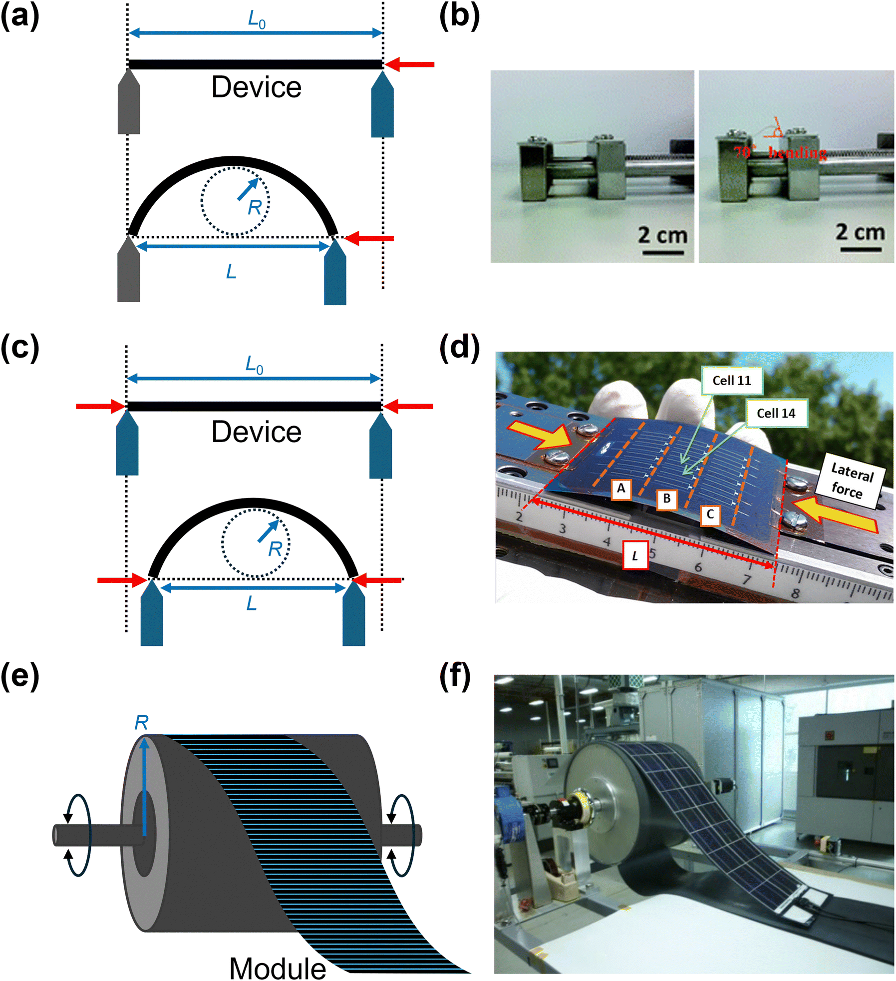 | ||
| Fig. 7 Schematic diagram and corresponding photographs of cyclic mechanical bending tests. (a) and (b) Two-stage bending system with one fixed stage and a movable stage on the opposite side, utilizing a specific bending angle. ((b) Adapted from ref. 72 with permission from Royal Society of Chemistry, Copyright 2016) (c) and (d) dual movable-stage system designed to track changes in the device's length under applied lateral force. Photograph presents a bent 100-μm-thick UTG-based flexible CIGS solar cell. ((d) Reproduced from ref. 49 with permission from Elsevier, Copyright 2015) (e) and (f) bending test unit for large-scale modules featuring coiling and uncoiling actions. ((f) Reproduced from ref. 122 with permission from EU PVSEC, Copyright 2010). | ||
6.2 Bending parameters and stress
Film-substrate system. The bending radius (R) is the most appropriate quantitative parameters to describe the flexibility of CIGS thin-film solar cells. Furthermore, the mechanical stress applied to the bent film can be estimated using this parameter. The bending radius is defined as:
 | (1) |
 | (2) |
Flexible electronic devices can be classified in the following terminologies, depending on the strain level:123
(i) ε < 2% (flexible electronics): devices with sufficiently thin (100 μm) substrate thickness, allowing them to be bent to a radius down to 10 mm, but unable to be stretched.
(ii) 2% < ε < 10% (compliant electronics): devices that can be bent to a radius of few millimeters and allow some in-plane loading with thicker substrates.
(iii) 10% < ε (stretchable electronics): devices that can be adapted to a wide range of surfaces exhibiting two-dimensional curvatures with a bending radius of few millimeters.
Multilayer system. In multilayer stacking structures, such as those of solar cell devices, the bending mechanism is more complex, as the mechanical properties of each layer should be taken into account. As shown in Fig. 8a, the position of the neutral plane znp is defined as:124
 | (3) |
 is the plane-strain modulus of the k-th layer
  . The strain induced by bending can be obtained by dividing the distance from the neutral plane z − znp by the bending radius R, which is the distance from the center of curvature to the neutral plane (Fig. 8b):
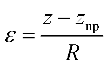 | (4) |
 | ||
| Fig. 8 (a) Schematic illustration of multilayer structure with n layers, where the k-th layer has a thickness tk, a Young's modulus Ek, and a Poisson's ratio vk at the middle position zk. (b) Bent state of multilayer structure with bending radius R. ((a) and (b) Reproduced from ref. 124 with permission from Elsevier, Copyright 2017) (c) mechanical bending in film-substrate system with deflection δ. (Reproduced from ref. 125 with permission from American Chemical Society, Copyright 2012). | ||
Furthermore, eqn (4) could be simplified by assuming that the thickness of the complete device (td) is largely dependent on the thickness of the substrate:
 | (5) |
Such approximation is often useful in rough practical evaluations; however, it should be noted that the mechanical properties of each layer might be significantly influenced by the fabrication process.
Stoney's formula. The Stoney's formula describes the residual stress in the film, under the assumption that the strain may be due to physical effects such as thermal expansion, epitaxial mismatch, and phase transformation. Furthermore, this formula also involves the following assumptions: (1) the substrate is thinner than the bending radius and the film is much thinner than the substrate (tf ≪ ts ≪ R); (2) the residual stress is homogeneous and uniform across the film thickness. As shown in Fig. 8c, the stress applied to the flexible electronics could be estimated based on the positional deflection caused by mechanical bending deformation. The film stress σf in a film–substrate system can be obtained by Stoney's formula as follows:126
 | (6) |
 | (7) |
 | (8) |
The CIGS solar cell is a multilayer stacked system; therefore, this method is typically used for analyzing the residual stress of the CIGS and Mo film or flexible substrate and its associated bending, rather than for assessing the device bending.
 | ||
| Fig. 9 (a) Photographs illustrating the application of a mechanical bending force to flexible CIGS solar cells at the specific bending angle and (b) bending angles increasing from 0° to 120° in a system with one side fixed and the other side movable. (c) and (d) Changes in device efficiency as a function of (c) bending angle and (d) number of bending cycles, with a bending angle of 70°. (Reproduced from ref. 72 with permission from Royal Society of Chemistry, Copyright 2016). | ||
6.3 Bending-induced phenomena
 | (9) |
 | (10) |
Positive and negative values of ε11 represents the tensile and compressive in-plane strain, respectively. Strain in crystals can alter the electronic band structure and, in turn, affect the electrical and optical properties. Although stress-induced changes in material properties can substantially affect the overall device performance, microscopic-scale changes in CIGS materials under mechanical bending have rarely been reported.
Park et al. explored the interplay between mechanicals stress and charge carrier distribution, both experimentally and theoretically, in devices with PI substrates.128 In their study, an atomic structure model was built by facing (1 1 2) facets at the GBs, which is the most frequently observed structure, as shown in Fig. 10. Under concave bending, axial compressive stress induced expansion of the GBs in the vertical direction of the axial stress. Conversely, axial tensile stress induced contraction of GBs under convex bending. The deformation of the crystal structure at GBs altered the defect formation energy, facilitating the generation of additional charges under concave bending, while hindering it under convex bending. Furthermore, alkali treatment reduced the intrinsic tensile stress. However, the residual stress originating from the CTE mismatch between the PI/Mo and CIGS layers could not be compensated by the external stress.129
 | ||
| Fig. 10 Deformation of atomic structure of (1 1 2) GBs under compressive and tensile mechanical stress. (Reproduced from ref. 128 with permission from Springer Nature, Copyright 2024). | ||
 | ||
| Fig. 11 (a) CIGS microstructure changes induced by various levels of mechanical stress. (b) Failure mechanism of CIGS thin-film solar cells under mechanical stress. (Reproduced from ref. 130 with permission from Elsevier, Copyright 2020). | ||
Macroscopic damages, such as delamination and cracks, could occur during mechanical bending, resulting in severe device failure. Thermal stress, intrinsic stress, and adhesion determined by the CTE of the materials or the fabrication process could affect the mechanical robustness of CIGS solar cells. In particular, in the delamination case, the adhesion between the CIGS absorber, back electrode, and substrate affects the robustness in the bent state. Kamikawa et al. from the AIST demonstrated that the Ar pressure (PAr) during the sputtering of Mo back contact on a PI flexible substrate largely influenced the intrinsic stress.132 As shown in Fig. 12, a large tensile stress was induced by a high PAr (larger than 0.5 Pa) and then released by the formation of cracks, markedly increasing the sheet resistance and reducing the FF value. This crack formation did not occur in Mo deposited on a SLG substrate, even at high PAr. Because PI films have a higher CTE than Mo, the PI substrate contracts more than Mo during the cooling process, causing compressive stress in the latter. Therefore, reducing the CTE of the PI substrate via physical or chemical modification strategies (such as post-treatment or chemical copolymerization) could effectively reduce the intrinsic stress and thus hinder potential macroscopic failure, while also achieving improved thermal stability.133
 | ||
| Fig. 12 (a) and (b) Photographs of Mo-coated Upilex®-50S and Upilex®-25SV5 PI substrate, on which Mo was deposited at Ar pressures of 0.1 and 0.3 Pa, respectively. (c) Estimated σMo values for various Ar pressures during sputtering. Plan-view SEM images of Mo layer deposited on PI substrate at Ar pressures of (d) and (e) 0.1 Pa and (f) and (g) 1.0 Pa. (Reproduced from ref. 132 with permission from Elsevier, Copyright 2022). | ||
 | ||
| Fig. 13 (a) and (b) Schematic illustration of piezo-phototronic effect in flexible CIGS solar cells and band diagrams under (a) compressive and (b) tensile strain. (c) and (d) Band diagram of flexible CIGS solar cells under (c) compressive and (d) tensile strain. (e) and (f) Changes in (e) VOC and JSC as well as (f) power conversion efficiency and FF in response to external compressive and tensile strains. (Reproduced from ref. 138 with permission from Elsevier, Copyright 2018). | ||
7. Advanced applications
7.1 Flexible bifacial CIGS solar cells
A recent approach for enhancing the efficiency of CIGS thin-film solar cells involves a bifacial configuration, which is particularly effective in various illumination conditions, such as those encountered in building-integrated photovoltaics (BIPVs) or installations on transportation vehicles and rooftops. Bifacial configurations maximize the energy yields of CIGS solar cells by collecting additional sunlight from the rear side, in addition to the front side. Such bifacial configurations can be achieved either by replacing the opaque metal back contact with a transparent layer or by forming double p–n junctions at the front and back of a central contact layer, which can be configured symmetrically or asymmetrically.139 These double-junction bifacial solar cells can potentially provide longer lifetimes by utilizing their front and rear sides for direct illumination. However, the requirement to deposit a double layer increases the production costs, which could limit their commercial viability.To enable light absorption from the rear side, the conventional opaque Mo metal back contact must be replaced with a TCO, such as ITO, fluorine-doped tin oxide, and AZO. However, unlike the interfacial MoSe2 layer that forms without significant issues at the CIGS/Mo back contact, a highly resistive GaOx thin layer often forms at the CIGS/TCO contact interface and acts as a detrimental hole barrier. Kim et al. demonstrated that the formation of this detrimental GaOx layer could be suppressed through the artificial incorporation of Na, which helps to enlarge the sizes of CIGS grains.47 The resulting devices were flexible and semitransparent, featuring an ultrathin CIGS layer (500 ± 20 nm) deposited on a 200-nm-thick UTG substrate, which provided increased transparency and average transmittance compared to ITO-coated SLG. Additionally, forming an ohmic-like contact at the CIGS/TCO back contact layer further enhanced the performance and long-term stability compared to the non-ohmic contact configuration.140,141
Recently, Yang et al. from the EMPA reported highly efficient bifacial CIGS solar cells, with efficiencies of 19.77% and 10.89% for front and rear-end illumination, respectively, which were achieved by lowering the growth temperature through Ag alloying (Fig. 14a).142 Notably, alloying with Ag reduces the melting point, allowing the growth temperature to be lowered from 453 to 303 °C. This low-temperature process enhances the Ga back gradient, which suppresses the back-interface recombination and minimizes the Ga interdiffusion toward the back contact, thereby preventing the formation of a GaOx layer at the CIGS/ITO interface. Furthermore, optical transfer matrix simulations showed that a high GGI and a wider bandgap at the back side facilitated the absorption of photons with wavelengths of 850 nm and promoted the transport of photogenerated carriers toward the absorber bulk. A theoretical study demonstrated that optimal bandgap grading, with a narrower bandgap at the front and a wider one at the rear of the CIGS layer, maximizes performance under both front and rear illumination by enhancing the electric field for efficient carrier transport.143 Taking advantage of the low-temperature process, a flexible bifacial CIGS solar cell was fabricated on an ITO-coated PI substrate, achieving efficiencies of 15.36% and 6.61% for front and rear-end illumination, respectively (Fig. 14b). The flexible PI substrate used in this study exhibited near-infrared transparency, suggesting the possibility of improving the JSC by replacing it with an even thinner and more transparent PI substrate.
 | ||
| Fig. 14 (a) Device structure of a bifacial CIGS solar cell fabricated on a glass substrate. (b) J–V curves of flexible bifacial CIGS device under front and rear illumination, with a simplified scheme of the device architecture. (Reproduced and adapted from ref. 142 with permission from Springer Nature, Copyright 2022). | ||
The lift-off process is another approach used to fabricate bifacial flexible CIGS solar cells by transferring the complete CIGS solar cell structure onto flexible substrates through mechanical cleaving. Unlike the bifacial configuration using a TCO back contact, the primary advantage of the lift-off process is that it allows the device to be fabricated using high-temperature growth conditions, which are typically used for conventional devices, as the initial deposition occurs on a rigid SLG substrate. In 1999, Tiwari et al. reported the application of the lift-off process on flexible CIGS thin-film solar cells.144 Specifically, they used a wet process to detach the flexible CIGS devices from the glass by dissolving the NaCl buffer layer between the glass and a spin-coated PI polymer substrate. More recently, Tseng et al. demonstrated a chemical–mechanical polishing lift-off transfer process that combined chemical and mechanical etching.48
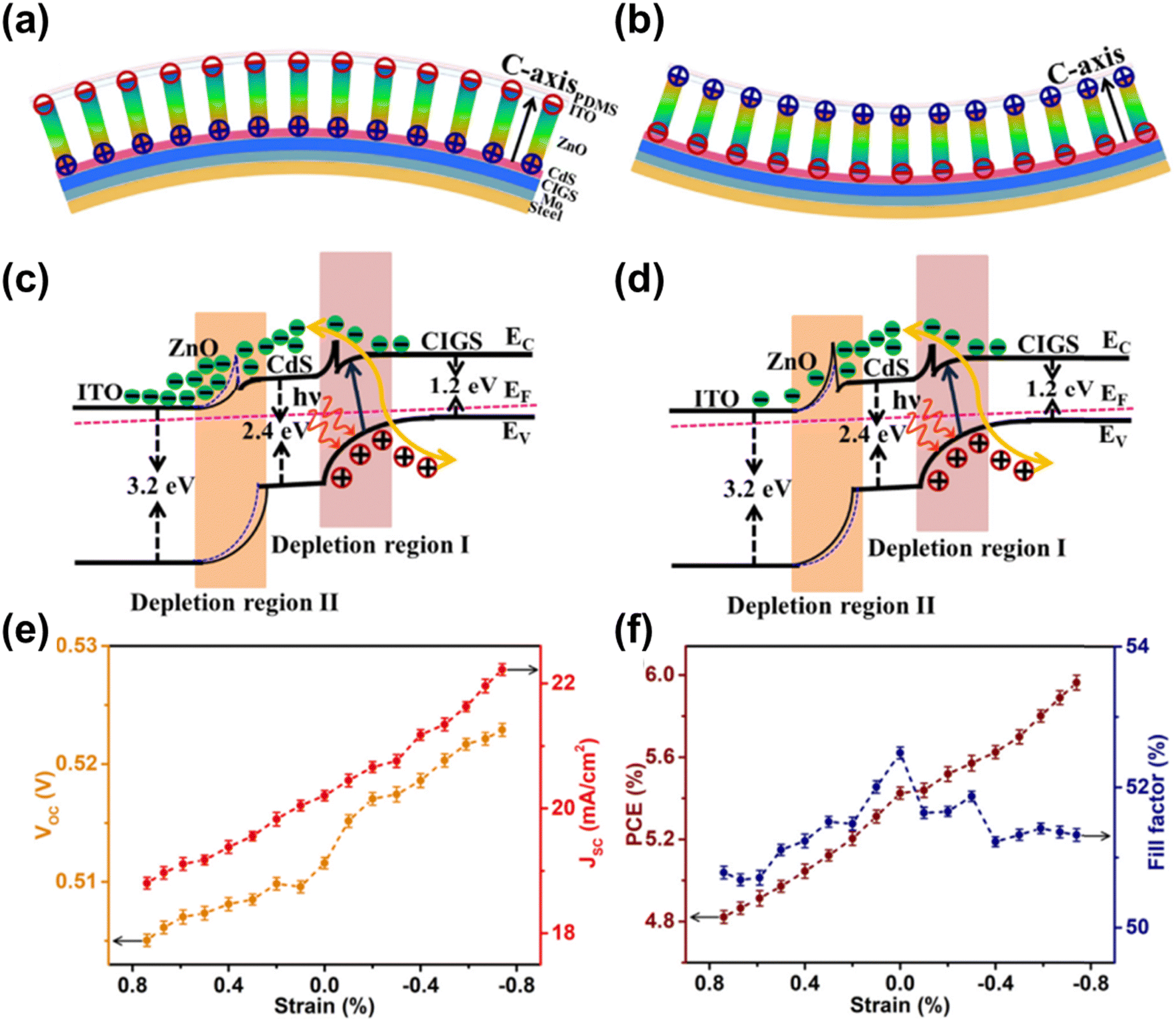
The most actively investigated lift-off method involves transferring a CIGS film to a flexible substrate through mechanical cleaving, which was mainly explored by a research group at Ritsumeikan University. As illustrated in Fig. 15a, flexible polymer films such as ETFE or FEP are attached to a full-substrate-type CIGS solar cell using epoxy glue. The device is then scribed using a blade to detach it from the Mo/SLG substrate. This method results in a high external quantum efficiency uniformity, with no cracks on the front and rear sides, as shown in Fig. 15b. The detachment relies on the van der Waals forces acting between the atomic layers of MoSe2, which form between the CIGS and the Mo back contact, enabling the cleavage of the CIGS layer from the Mo. To ensure a clear and stable cleavage with minimal damage, Nishimura et al. targeted the cleavage of weak chemical bonds in MoSe2 by controlling the orientation of the MoSe2 layer.44 Their results demonstrated that the CIGS lift-off cells maintained 95% of their initial efficiency when the c-axis of the MoSe2 layer was oriented perpendicular to the Mo surface (Fig. 15c). This remarkable performance was attributed to the clean cleavage of the CIGS devices, with almost no cracks or contamination. Furthermore, minimizing the presence of MoSe2 through the lift-off process could help to reduce the rollover effect in J–V curves.145 Additionally, the introduction of an ultrathin Au layer with a thickness of 5 nm between the CIGS and AZO transparent back contact formed an ohmic contact, thereby lowering the shunt resistance.43 This bilayer back contact, comprising ultrathin Au and AZO, was deposited using a low-temperature process, which prevented the formation of undesirable Ga2O3 compounds at the interface.
 | ||
| Fig. 15 (a) Schematic illustration of lift-off process for superstrate flexible CIGS solar cells using an ETFE film. (Adapted from ref. 43 with permission from Elsevier, Copyright 2020) (b) mapping of local external quantum efficiency at 780 nm wavelength for substrate-type CIGS solar cells with an ETFE film, before and after the lift-off process. (Reproduced from ref. 146 with permission from Elsevier, Copyright 2018) (c) J–V curves of flexible bifacial CIGS solar cells under front and rear illumination. (Reproduced from ref. 44 with permission from American Chemical Society, Copyright 2020). | ||
However, unlike the bifacial configuration using a TCO back contact, scaling up the lift-off process from the laboratory to the industrial scale is challenging. This is because the method involves additional time-consuming mechanical steps, rendering it unsuitable for mass production or roll-to-roll processing. Furthermore, issues such as unavoidable mechanical damage, cracks, and poor adhesion between the transferred layers and flexible substrates must be addressed to improve the viability of this technique for large-scale applications.
7.2 Flexible CIGS/perovskite tandem solar cells
Tandem solar cells comprise multiple junctions and combine more than two solar cells with different bandgaps, enabling the absorption of a wide range of wavelengths. In these configurations, wide-bandgap materials are used in the top cells to absorb light at shorter wavelengths, while narrow-bandgap materials are employed in the bottom cells to absorb longer wavelengths. In tandem solar cells, CIGS can be an ideal candidate material for the bottom cell when paired with a perovskite top cell, owing to its broad light absorption range and tunable bandgap, which provides high tunability in optical absorption. Perovskite materials, known for their excellent light absorption, have driven rapid advances in optoelectronic devices over the past decade. However, perovskites are highly susceptible to degradation by oxygen and moisture, which can substantially reduce their stability. Consequently, the stability of CIGS is crucial for ensuring the overall stability and longevity of tandem solar cells.As illustrated in Fig. 16a, the two-terminal (2T) structure combines two cells connected by a conductive interface layer, whereas the four-terminal (4T) configuration involves the mechanical stacking of two independent cells. To date, the most advanced CIGS–perovskite tandem cells on rigid substrates have achieved efficiencies of 29.9% and 24.2% for the 4T147 and 2T148 configurations, respectively. However, only few studies have explored flexible CIGS–perovskite tandem solar cells, owing to the high technological demands of both types of cells, as well as the complexities involved in cell connection techniques, as illustrated in Fig. 16b. In particular, 2T configurations are rarely reported, owing to the difficult selection of a suitable interconnecting layer that is compatible with both cells. In contrast, advances in 4T devices have exhibited a steady progress. A summary of the efficiency improvements of flexible CIGS/perovskite tandem solar cell is presented in Table 4. The reported bandgap ranges for perovskite top and CIGS bottom cells are 1.60–1.75 eV and 1.07–1.15 eV, respectively.
 | ||
| Fig. 16 (a) Schematic illustration of 2T and 4T configurations of CIGS–perovskite tandem solar cells. (b) Diagram showing recent improvements in the efficiency of 2T and 4T flexible CIGS–perovskite tandem solar cells. | ||
| Year | Effa (%) | Cell | Material | E g (eV) | Substrate | V OC (V) | J SC (mA cm−2) | FF (%) | Eff (%) | Ref. | |
|---|---|---|---|---|---|---|---|---|---|---|---|
| a Efficiency. b The performance of the CIGS bottom cells refers to the filtered devices. c Monolithic minimodules. | |||||||||||
| 2T | 2019 | 13.2 | Top | MAPbI3 | 1.60 | PI | 1.751 | 16.3 | 46.6 | 149 | |
| Bottomb | CIGS | 1.15 | |||||||||
| 2023 | 23.6 | Top | Perovskite | — | — | — | — | — | — | 150 | |
| Bottom | CIGS | — | |||||||||
| 2024 | 18.1c | Top | (FAPbI3)0.83(MAPbBr3)0.17 | — | SS | 1.645 | 17.7 | 62 | — | 151 | |
| Bottom | CIGS | — | |||||||||
| 4T | 2017 | 18.2 | Top | MAPbI3 | 1.60 | Flexible foil | 1.08 | 16.1 | 68.5 | 12.2 | 152 |
| Bottom | CIGS | 1.10 | PI | 0.63 | 12.6 | 77.3 | 6.0 | ||||
| 2018 | 19.6 | Top | MAPbI3 | 1.60 | Flexible foil | 1.06 | 18.7 | 68.9 | 14.0 | 153 | |
| Bottom | CIGS | — | PI | 0.65 | 12.0 | 71.6 | 5.6 | ||||
| 2020 | 21.1 | Top | FA0.8Cs0.2Pb(I0.7Br0.3) | 1.75 | PET | 1.19 | 16.4 | 77.5 | 15.0 | 154 | |
| Bottom | CIGS | — | SS | 0.63 | 12.8 | 75.5 | 6.0 | ||||
| 2023 | 21.6 | Top | Perovskite | — | PEN | 1.02 | 20.5 | 73.7 | 15.6 | 155 | |
| Bottom | CIGS | — | PI | 0.66 | 12.4 | 76.7 | 6.3 | ||||
| 2024 | 26.57 | Top | Cs0.05(FA0.77MA0.23)0.95Pb(I0.77Br0.23)3 | 1.67 | PEN | 1.18 | 18.73 | 80.14 | 17.75 | 156 | |
| Bottom | CIGS | 1.07 | PI | 0.61 | 20.02 | 72.23 | 8.82 | ||||
| 2022 | 18.4c | Top | Perovskite | — | PEN | 3.32 | 4.73 | 69.2 | 10.9 | 157 | |
| Bottom | CIGS | — | PI | 3.53 | 3.18 | 66.9 | 7.5 | ||||
In 2017, a research group at the EMPA first reported a proof-of-concept study of a 4T flexible CIGS–perovskite tandem cell, achieving an efficiency of 18.2% using vacuum-assisted deposition for the perovskite layer.152 A year later, they achieved an increased efficiency of 19.6% by replacing the AZO conducting layer with InZnO.153 In both cases, they employed a two-step hybrid method, involving the thermal evaporation of the PbI2 source followed by the solution coating of methylammonium iodide (MAI). This approach provided precise control of the layer thickness, which contributed to achieving an optimal JSC match between the cells. To date, most advances in flexible tandem cells have been achieved by optimizing the fabrication or passivation processes of perovskite top cells or interconnecting layers. This is because the fabrication methods for CIGS bottom cells are already well-optimized and commercially accessible. For instance, Li et al. developed semitransparent 4T CIGS–perovskite solar cells by integrating perovskite top cells with flexible CIGS bottom solar cells commercially available from MiaSole.154 On the other hand, a research group at Wuhan University focused on achieving an optimal GGI double grading in tandem configurations.155 Furthermore, they enhanced the growth of CIGS thin films by incorporating Na and Rb, while Ag alloying further improved the crystallinity.
Two years after the first report of the flexible 4T tandem device, in 2019 Fu et al. at the EMPA reported the development of a 2T flexible CIGS–perovskite solar cell using a PI substrate.149 Owing to the challenges associated with the selection of a suitable interconnecting layer for flexible substrates, only a limited number of flexible 2T tandem devices have been reported to date. The highest efficiency achieved for a flexible 2T device was 23.6%, as presented at the PSCO 2023 6th International Conference on Perovskite Solar Cells and Optoelectronic, although detailed experimental data and device information were not provided.
In terms of scaling up, a flexible 4T CIGS–perovskite tandem minimodule achieved an efficiency of 18.4% on an aperture area of 2.03 cm2.157 This minimodule employed a monolithically integrated configuration and achieved a cell-to-module loss of less than 10% through optimized laser scribing, even on a soft polyethylene naphthalate (PEN) substrate. A recent study reported a flexible monolithic minimodule for a 2T tandem device with an efficiency of 18.1%.151
To date, the highest efficiency in flexible CIGS–perovskite tandem solar cells has been achieved using a 4T configuration. Recently, researchers at Wuhan University set a new record efficiency of 26.57% for fully flexible CIGS–perovskite tandem solar cells (Fig. 17).156 This breakthrough was primarily attributed to a dual-passivation strategy that passivated both the grains and interfaces of wide-bandgap perovskite solar cells. Although the study examined the mechanical durability through bending tests, these experiments were only conducted on flexible perovskite cells. Despite their significant commercialization potential, the mechanical stability and bending resistance of flexible CIGS–perovskite tandem cells remain underexplored. Thus, further investigations of their mechanical stability and durability are essential to ensure their reliability in practical applications.
 | ||
| Fig. 17 (a) Schematic illustration of 4T perovskite–CIGS tandem solar cells. (b) J–V curves of flexible CIGS, filtered CIGS, and perovskite devices. (c) External quantum efficiency curves of flexible perovskite and filtered CIGS solar cells, also showing integrated JSC values. (Reproduced from ref. 156 with permission from Wiley, Copyright 2024). | ||
7.3 Other applications
In addition to solar energy harvesting, flexible CIGS solar cells also have promising potential in space applications such as powering low-orbit satellites, owing to their light weight, flexibility, and high radiation resistance. CIGS cells provide superior radiation resistance compared to conventional crystalline Si cells, making them ideal for use in high-altitude or space environments.158 Their high specific power is another attractive feature for space applications.9 For instance, Banik et al. reported that a thin Si oxycarbonitride (SiCNO) coating on flexible CIGS solar cells serves as an effective passive radiative cooler, substantially increasing the heat emission into space with minimal spectral losses.159 Furthermore, the performance of flexible CIGS solar cells has been tested under the low-intensity and low-temperature conditions typical of various planetary environments, including Earth, Mars, Jupiter, and Saturn.160 These investigations showed that, as the temperature decreased, the VOC and FF values increased for both relaxed and metastable states, because defect states in the bandgap were not activated at these temperatures. However, proton irradiation can deteriorate the performance of flexible devices by creating defect states, particularly under low-intensity and low-temperature conditions. These findings highlight the potential of flexible CIGS solar cells as power sources in harsh aerospace environments. Furthermore, flexible CIGS solar cells have been investigated for medical applications, such as skin dosimeters for electron radiotherapy, exhibiting small error margins even under concave and convex bending conditions.1618. Future perspectives
CIGS solar cells have reached a market share that rivals that of Si-based cells. To remain competitive in the solar cell market, transitioning to high-efficiency and lightweight flexible devices with lower production costs is a crucial target. Among various flexible substrates proposed to date, PI and SS are the most commonly used at both laboratory and industrial scales. To date, PI-based devices have demonstrated the best performance, while most commercially available flexible CIGS solar panels have adopted SS due to its high heat resistance. Therefore, lowering the growth temperature is critical for expanding the use of PI substrates, which is suitable for low-cost, lightweight monolithic module manufacturing. Additionally, precise composition control, such as adjusting Ga grading, boosts efficiency by maximizing carrier collection. Furthermore, flexible substrates lack alkali elements, unlike SLG, the artificial incorporation of these elements is essential. The AlkF PDT method has proven to be particularly effective for this purpose. Notably, the use of multiple types of alkali further enhanced the performance, particularly in PI-based flexible devices. Scalable fabrication processes for CIGS solar cells are well established, enabling larger module areas and the use of monolithic integration techniques, such as optimized laser scribing. To enhance their flexibility and robustness, mechanical bending-induced failure has been thoroughly studied, revealing that both microscopic and macroscopic deformations can lead to performance decreases. In particular, optimizing the CTE difference between the CIGS, back contact, and substrates is critical to minimizing microscopic damage.Among advanced applications, highly efficient flexible bifacial devices exhibited versatile properties for indoor and outdoor power generation, particularly in building-integrated photovoltaics. The stable and tunable bandgap characteristics of CIGS solar cells make them suitable for use in the bottom cells of tandem solar devices, combined with wide-bandgap perovskite top cells. The 2T and 4T configurations of such flexible tandem cells achieved efficiencies of 23.6% and 26.57%, respectively. In particular, the performance of CIGS/perovskite tandem cells was improved through optimal GGI double grading, Na and Rb incorporation for thin-film growth, and Ag alloying for enhanced crystallinity. Developing tandem solar cells on flexible substrates requires advanced fabrication techniques, along with the optimization of the top and bottom cells as well as the interconnecting layer. Therefore, extensive research is required to further improve the performance and mechanical durability of such cells, particularly the 2T tandem configurations. Despite these challenges, flexible CIGS–perovskite tandem solar cells hold significant promise as a solution for lightweight and portable energy systems.
Data availability
No primary research results, software or code have been included and no new data were generated or analysed as part of this review.Conflicts of interest
There are no conflicts to declare.Acknowledgements
This research was supported by the National Research Foundation of Korea (NRF) under grants NRF-2018R1A6A1A03025340 and RS-2024-00355905. Additionally, it received funding from the Technology Development Program for the solving of climate change (grant NRF-2022M3J1A1064229) The first author, H. K. P., also gratefully acknowledges fellowship support from the Hyundai Motor Chung Mong-Koo Foundation.References
- J. Keller, K. Kiselman, O. Donzel-Gargand, N. M. Martin, M. Babucci, O. Lundberg, E. Wallin, L. Stolt and M. Edoff, Nat. Energy, 2024, 9, 467–478 CrossRef CAS.
- M. Nakamura, K. Yamaguchi, Y. Kimoto, Y. Yasaki, T. Kato and H. Sugimoto, IEEE J. Photovolt., 2019, 9, 1863–1867 Search PubMed.
- https://www.pv-magazine.com/2022/10/11/swiss-scientists-achieve-22-2-efficiency-forflexible-cigs-solar-cell/ .
- S.-H. Wei and A. Zunger, J. Appl. Phys., 1995, 78, 3846–3856 CrossRef CAS.
- N. Khoshsirat, N. A. Md Yunus, M. N. Hamidon, S. Shafie and N. Amin, Optik, 2015, 126, 681–686 CrossRef CAS.
- J. Ramanujam and U. P. Singh, Energy Environ. Sci., 2017, 10, 1306–1319 RSC.
- T. Feurer, P. Reinhard, E. Avancini, B. Bissig, J. Löckinger, P. Fuchs, R. Carron, T. P. Weiss, J. Perrenoud, S. Stutterheim, S. Buecheler and A. N. Tiwari, Prog. Photovoltaics Res. Appl., 2016, 25, 645–667 CrossRef.
- S. Ishizuka, Y. Kamikawa and J. Nishinaga, npj Flexible Electron., 2022, 6, 90 CrossRef CAS.
- J. Ramanujam, D. M. Bishop, T. K. Todorov, O. Gunawan, J. Rath, R. Nekovei, E. Artegiani and A. Romeo, Prog. Mater. Sci., 2020, 110, 100619 CrossRef CAS.
- N. Mufti, T. Amrillah, A. Taufiq, Sunaryono, Aripriharta, M. Diantoro, Zulhadjri and H. Nur, Sol. Energy, 2020, 207, 1146–1157 CrossRef CAS.
- S. Wagner, J. L. Shay, P. Migilorato and H. M. Kasper, Appl. Phys. Lett., 1974, 25, 434–435 CrossRef CAS.
- W. E. Devaney, W. S. Chen, J. M. Stewart and R. A. Mickelsen, IEEE Trans. Electron Devices, 1990, 37, 428–433 CrossRef CAS.
- A. M. Gabor, J. R. Tuttle, D. S. Albin, M. A. Contreras, R. Noufi and A. M. Hermann, Appl. Phys. Lett., 1994, 65, 198–200 CrossRef CAS.
- C. Zhao, S. Yu, W. Tang, X. Yuan, H. Zhou, T. Qi, X. Zheng, D. Ning, M. Ma, J. Zhu, J. Zhang, C. Yang and W. Li, Mater. Rep.: Energy, 2023, 3, 100214 CAS.
- P. Jackson, D. Hariskos, R. Wuerz, W. Wischmann and M. Powalla, Phys. Status Solidi RRL, 2014, 8, 219–222 CrossRef CAS.
- P. Jackson, R. Wuerz, D. Hariskos, E. Lotter, W. Witte and M. Powalla, Phys. Status Solidi RRL, 2016, 10, 583–586 CrossRef CAS.
- D. M. Basol, V. K. Kapur, C. R. Leidhom, A. Halani and K. Gledhill, Sol. Energy Mater. Sol. Cells, 1996, 43, 93–98 CrossRef.
- A. N. Tiwari, M. Krejci, F.-J. Haug and H. Zogg, Prog. Photovoltaics Res. Appl., 1999, 7, 393–397 CrossRef CAS.
- D. Rudmann, D. Brémaud, H. Zogg and A. N. Tiwari, J. Appl. Phys., 2005, 97, 084903 CrossRef.
- S. Ishizuka, H. Hommoto, N. Kido, K. Hashimoto, A. Yamada and S. Niki, Appl. Phys. Express, 2008, 1, 124105 Search PubMed.
- R. Caballero, C. A. Kaufmann, T. Eisenbarth, T. Unold, S. Schorr, R. Hesse, R. Klenk and H. W. Schock, Phys. Status Solidi A, 2009, 206, 1049–1053 CrossRef CAS.
- R. Caballero, C. A. Kaufmann, T. Eisenbarth, T. Unold, R. Klenk and H. W. Schock, Prog. Photovoltaics Res. Appl., 2011, 19, 547–551 CrossRef CAS.
- T. Nakada, T. Kuraishi, T. Inoue and T. Mise, 2010 35th IEEE Photovoltaic Specialists Conference DOI:10.1109/PVSC.2010.5615947.
- A. Chirilă, D. Guettler, P. Bloesch, S. Nishiwaki, S. Seyrling, S. Buecheler, R. Verma, F. Pianezzi, Y. E. Romanyuk, G. Bilger, R. Ziltener, D. Brémaud and A. N. Tiwari, 2010 35th IEEE Photovoltaic Specialists Conference DOI:10.1109/PVSC.2010.5616887.
- A. Chirila, S. Buecheler, F. Pianezzi, P. Bloesch, C. Gretener, A. R. Uhl, C. Fella, L. Kranz, J. Perrenoud, S. Seyrling, R. Verma, S. Nishiwaki, Y. E. Romanyuk, G. Bilger and A. N. Tiwari, Nat. Mater., 2011, 10, 857–861 CrossRef CAS PubMed.
- A. Chirila, P. Reinhard, F. Pianezzi, P. Bloesch, A. R. Uhl, C. Fella, L. Kranz, D. Keller, C. Gretener, H. Hagendorfer, D. Jaeger, R. Erni, S. Nishiwaki, S. Buecheler and A. N. Tiwari, Nat. Mater., 2013, 12, 1107–1111 CrossRef CAS PubMed.
- R. Carron, S. Nishiwaki, T. Feurer, R. Hertwig, E. Avancini, J. Löckinger, S. C. Yang, S. Buecheler and A. N. Tiwari, Adv. Energy Mater., 2019, 9, 1900408 CrossRef.
- https://www.windynation.com/products/100-watt-flex-panel .
- https://miasole.com/products/ .
- https://www.bougerv.com/products/200w-flexible-solar-panel .
- https://www.renogy.com/renogy-150-watt-cigs-monocrystalline-solar-panel/ .
- https://www.renogy.com/100-watt-12-volt-flexible-monocrystalline-solar-panel/ .
- R. Lee, H. Lee, D. Kim and J. Yoon, Energy Sci. Eng., 2021, 10, 292–307 CrossRef.
- W. K. Batchelor, I. L. Repins, J. Schaefer and M. E. Beck, Sol. Energy Mater. Sol. Cells, 2004, 83, 67–80 CrossRef CAS.
- F. Kessler and D. Rudmann, Sol. Energy, 2004, 77, 685–695 CrossRef CAS.
- S. Niki, M. Contreras, I. Repins, M. Powalla, K. Kushiya, S. Ishizuka and K. Matsubara, Prog. Photovoltaics Res. Appl., 2010, 18, 453–466 CrossRef CAS.
- T. Yagioka and T. Nakada, Appl. Phys. Express, 2009, 2, 072201 CrossRef.
- P. Reinhard, A. Chirilă, P. Blösch, F. Pianezzi, S. Nishiwaki, S. Buechelers and A. N. Tiwari, IEEE 38th Photovoltaic Specialists Conference (PVSC) PART 2, 2012 DOI:10.1109/PVSC-Vol2.2012.6656789.
- J.-K. Sim, S. Kang, R. Nandi, J.-Y. Jo, K.-U. Jeong and C.-R. Lee, Sol. Energy, 2018, 162, 357–363 CrossRef CAS.
- K. Herz, A. Eicke, F. Kessler, R. Wächter and M. Powalla, Thin Solid Films, 2003, 431–432, 392–397 CrossRef CAS.
- J. Chantana, B. Ergashev, Y. Kawano and T. Minemoto, Sol. Energy Mater. Sol. Cells, 2023, 263, 112589 CrossRef CAS.
- T. Minemoto, Y. Abe, T. Anegawa, S. Osada and H. Takakura, Jpn. J. Appl. Phys., 2010, 49, 04DP06 CrossRef.
- N. Hamada, T. Nishimura, J. Chantana, Y. Kawano, T. Masuda and T. Minemoto, Sol. Energy, 2020, 199, 819–825 CrossRef CAS.
- T. Nishimura, N. Hamada, J. Chantana, A. Mavlonov, Y. Kawano, T. Masuda and T. Minemoto, ACS Appl. Energy Mater., 2020, 3, 9504–9508 CrossRef CAS.
- M. G. Faraj, K. Ibrahim and A. Salhin, Int. J. Polym. Mater., 2011, 60, 817–824 CrossRef CAS.
- A. Illiberi, C. Frijters, M. Ruth, D. Bremaud, P. Poodt, F. Roozeboom and P. J. Bolt, J. Vac. Sci. Technol., 2018, 36, 051511 CrossRef.
- D. Kim, S. S. Shin, S. M. Lee, J. S. Cho, J. H. Yun, H. S. Lee and J. H. Park, Adv. Funct. Mater., 2020, 30, 2001775 CrossRef CAS.
- K. C. Tseng, Y. T. Yen, S. R. Thomas, H. W. Tsai, C. H. Hsu, W. C. Tsai, C. H. Shen, J. M. Shieh, Z. M. Wang and Y. L. Chueh, Nanoscale, 2016, 8, 5181–5188 RSC.
- A. Gerthoffer, F. Roux, F. Emieux, P. Faucherand, H. Fournier, L. Grenet and S. Perraud, Thin Solid Films, 2015, 592, 99–104 CrossRef CAS.
- J. Chen, H. Shen, Z. Zhai, Y. Li and Y. Lin, J. Mater. Sci.: Mater. Electron., 2019, 30, 11754–11763 CrossRef CAS.
- Y.-C. Wang, T.-T. Wu and Y.-L. Chueh, Mater. Chem. Phys., 2019, 234, 329–344 CrossRef CAS.
- R. Wuerz, A. Eicke, F. Kessler, S. Paetel, S. Efimenko and C. Schlegel, Sol. Energy Mater. Sol. Cells, 2012, 100, 132–137 CrossRef CAS.
- L. Zortea, S. Nishiwaki, T. P. Weiss, S. Haass, J. Perrenoud, L. Greuter, T. Feurer, G. Palaniswamy, S. Buecheler and A. N. Tiwari, Sol. Energy, 2018, 175, 25–30 CrossRef CAS.
- S. Hamtaei, G. Brammertz, J. Poortmans and B. Vermang, npj Flexible Electron., 2023, 7, 36 CrossRef CAS.
- J. Chantana, S. Teraji, T. Watanabe and T. Minemoto, Sol. Energy, 2018, 173, 126–131 CrossRef CAS.
- T. Eisenbarth, R. Caballero, C. A. Kaufmann, A. Eicke and T. Unold, Prog. Photovoltaics Res. Appl., 2012, 20, 568–574 CrossRef CAS.
- Y. Kawano, J. Chantana, T. Nishimura, A. Mavlonov and T. Minemoto, Sol. Energy, 2020, 204, 231–237 CrossRef CAS.
- B. Li, J. Li, L. Wu, W. Liu, Y. Sun and Y. Zhang, J. Alloys Compd., 2015, 627, 1–6 CrossRef CAS.
- W.-S. Liu, H.-C. Hu, N.-W. Pu and S.-C. Liang, J. Alloys Compd., 2015, 631, 146–152 CrossRef CAS.
- P. Misra, S. R. Atchuta, S. Mandati, B. V. Sarada, T. N. Rao and S. Sakthivel, Sol. Energy, 2021, 214, 471–477 CrossRef CAS.
- R. Wuerz, A. Eicke, M. Frankenfeld, F. Kessler, M. Powalla, P. Rogin and O. Yazdani-Assl, Thin Solid Films, 2009, 517, 2415–2418 CrossRef CAS.
- Y. D. Liu, Y. Q. Cao, J. L. Tang, J. Yu and B. Lin, Energy Technol., 2024, 12, 2300871 CrossRef CAS.
- C. Zhang, T. Qi, W. Wang, C. Zhao, S. Xu, M. Ma, Y. Feng, W. Li, M. Chen, C. Yang and W. Li, Sol. Energy, 2021, 230, 1033–1039 CrossRef CAS.
- W. Thongkham, A. Pankiew, K. Yoodee and S. Chatraphorn, Sol. Energy, 2013, 92, 189–195 CrossRef CAS.
- H. Kim and S. P. Cias, Sol. Energy Mater. Sol. Cells, 2024, 272, 112888 CrossRef CAS.
- P. Blösch, D. Güttler, A. Chirila and A. N. Tiwari, Thin Solid Films, 2011, 519, 7453–7457 CrossRef.
- S. Ishizuka, A. Yamada, K. Matsubara, P. Fons, K. Sakurai and S. Niki, Appl. Phys. Lett., 2008, 93, 124105 CrossRef.
- S. Ishizuka, T. Yoshiyama, K. Mizukoshi, A. Yamada and S. Niki, Sol. Energy Mater. Sol. Cells, 2010, 94, 2052–2056 CrossRef CAS.
- V. R. Voggu, J. Sham, S. Pfeffer, J. Pate, L. Fillip, T. B. Harvey, R. M. Brown and B. A. Korgel, ACS Energy Lett., 2017, 2, 574–581 CrossRef CAS.
- S. Calnan and A. N. Tiwari, Thin Solid Films, 2010, 518, 1839–1849 CrossRef CAS.
- C. H. Chung, T. B. Song, B. Bob, R. Zhu, H. S. Duan and Y. Yang, Adv. Mater., 2012, 24, 5499–5504 CrossRef CAS PubMed.
- W.-C. Tsai, S. R. Thomas, C.-H. Hsu, Y.-C. Huang, J.-Y. Tseng, T.-T. Wu, C.-H. Chang, Z. M. Wang, J.-M. Shieh, C.-H. Shen and Y.-L. Chueh, J. Mater. Chem. A, 2016, 4, 6980–6988 RSC.
- D.-H. Cho, W.-J. Lee, T.-H. Hwang, J. Huh, S. S. Yoon and Y.-D. Chung, J. Power Sources, 2024, 603, 234443 CrossRef CAS.
- Y. Liu, S. Zeder, S. Lin, R. Carron, G. Grossmann, S. Bolat, S. Nishiwaki, F. Clemens, T. Graule, A. N. Tiwari, H. Wu and Y. E. Romanyuk, Sci. Technol. Adv. Mater., 2019, 20, 26–34 CrossRef CAS PubMed.
- S.-T. Kim, H.-J. Jeong, S. K. Lee, J.-S. Yoo and J.-H. Jang, 47th IEEE Photovoltaic Specialists Conference (PVSC), 2020 DOI:10.1109/PVSC45281.2020.9300839.
- T. S. Lopes, J. P. Teixeira, M. A. Curado, B. R. Ferreira, A. J. N. Oliveira, J. M. V. Cunha, M. Monteiro, A. Violas, J. R. S. Barbosa, P. C. Sousa, I. Çaha, J. Borme, K. Oliveira, J. Ring, W. C. Chen, Y. Zhou, K. Takei, E. Niemi, F. L. Deepak, M. Edoff, G. Brammertz, P. A. Fernandes, B. Vermang and P. M. P. Salomé, npj Flexible Electron., 2023, 7, 4 CrossRef CAS.
- A. M. Amare, I. Hwang, I. Jeong, J. H. Park, J. G. An, S. Song, Y.-J. Eo, A. Cho, J.-S. Cho, S. K. Ahn, J. Yoo, S. J. Ahn, J. Gwak, H.-W. Park, J. H. Yun, K. Kim and D. Shin, Curr. Photovoltaics Res., 2023, 11, 8–12, DOI:10.21218/CPR.2023.11.1.008.
- M. Acciarri, A. Le Donne, S. Marchionna, M. Meschia, J. Parravicini, A. Gasparotto and S. Binetti, Sol. Energy, 2018, 175, 16–24 CrossRef CAS.
- S. Mandati, P. Misra, D. Boosagulla, N. R. Tata and S. V. Bulusu, Ind. Eng. Chem. Res., 2021, 60, 2197–2205 CrossRef CAS.
- G. Regmi, S. Rijal and S. Velumani, Curr. Appl. Phys., 2024, 57, 49–58 CrossRef.
- D.-Y. Jung, Y.-R. Jeong, M. S. Mina, S.-E. Lee, E. Enkhbayar and J. Kim, Curr. Appl. Phys., 2022, 41, 66–72 CrossRef.
- S. C. Chen, N. Z. She, K. H. Wu, Y. Z. Chen, W. S. Lin, J. X. Li, F. I. Lai, J. Y. Juang, C. W. Luo, L. T. Cheng, T. P. Hsieh, H. C. Kuo and Y. L. Chueh, ACS Appl. Mater. Interfaces, 2017, 9, 14006–14012 CrossRef CAS PubMed.
- T. Zhang, Y. Yang, D. Liu, S. C. Tse, W. Cao, Z. Feng, S. Chen and L. Qian, Energy Environ. Sci., 2016, 9, 3674–3681 RSC.
- G. Albalawneh and M. Ramli, ECS J. Solid State Sci. Technol., 2020, 9, 0161013 Search PubMed.
- J. Chantana, T. Watanabe, S. Teraji and T. Minemoto, Sol. Energy Mater. Sol. Cells, 2016, 157, 750–756 CrossRef CAS.
- Y. Kawano, J. Chantana, T. Nishimura, A. Mavlonov and T. Minemoto, J. Alloys Compd., 2022, 899, 163276 CrossRef CAS.
- H. K. Park, Y. Cho, K. Kim, I. Jeong, J. Gwak, J. H. Yun and W. Jo, ACS Appl. Mater. Interfaces, 2022, 14, 34697–34705 CrossRef CAS PubMed.
- Y. H. Wang, P. H. Ho, W. C. Huang, L. H. Tu, H. F. Chang, C. H. Cai and C. H. Lai, ACS Appl. Mater. Interfaces, 2020, 12, 28320–28328 CrossRef CAS PubMed.
- H. Yan, W. Wang, J. Luo, Z. Chi, J. Gong, J. Li and X. Xiao, ACS Appl. Mater. Interfaces, 2024, 16, 54171–54177 CrossRef PubMed.
- S. Kim, H. Yoo, T. R. Rana, T. Enkhbat, G. Han, J. Kim, S. Song, K. Kim, J. Gwak, Y. J. Eo and J. H. Yun, Adv. Energy Mater., 2018, 8, 1801501 CrossRef.
- K. Kim, J. Kim, M. G. Gang, S.-H. Kim, S. Song, Y. Cho, D. Shin, Y.-J. Eo, I. Jeong, S. K. Ahn, A. Cho, J. Kim, S. Yoon, P.-P. Choi, W. Jo, J. H. Kim, J. Gwak and J. H. Yun, Sol. Energy Mater. Sol. Cells, 2019, 195, 280–290 CrossRef CAS.
- Y. Wang, S. Lv and Z. Li, J. Mater. Sci. Technol., 2022, 96, 179–189 CrossRef CAS.
- P. Blösch, S. Nishiwaki, A. Chirilă, L. Kranz, C. Fella, F. Pianezzi, C. Adelhelm, E. Franzke, S. Buecheler and A. N. Tiwari, Thin Solid Films, 2013, 535, 214–219 CrossRef.
- R. Caballero, C. A. Kaufmann, T. Eisenbarth, M. Cancela, R. Hesse, T. Unold, A. Eicke, R. Klenk and H. W. Schock, Thin Solid Films, 2009, 517, 2187–2190 CrossRef CAS.
- S.-T. Kim, H.-J. Jeong, Y.-C. Kim, V. Bhatt, M. Kumar, J.-H. Yun and J.-H. Jang, Energy Rep., 2021, 7, 2255–2261 CrossRef.
- X. Ma, Y. Ma, S. Yang, C. Yang, T. Lin, K. Wang and X. Xiao, Sol. Energy, 2018, 173, 1080–1086 CrossRef CAS.
- F. Kessler, D. Herrmann and M. Powalla, Thin Solid Films, 2005, 480–481, 491–498 CrossRef CAS.
- D. Colombara, K. Conley, M. Malitckaya, H.-P. Komsa and M. J. Puska, J. Mater. Chem. A, 2020, 8, 6471–6479 RSC.
- K. Kim, I. Jeong, Y. Cho, D. Shin, S. Song, S. K. Ahn, Y.-J. Eo, A. Cho, C. Jung, W. Jo, J. H. Kim, P.-P. Choi, J. Gwak and J. H. Yun, Nano Energy, 2020, 67, 10421 Search PubMed.
- R. Wuerz, W. Hempel and P. Jackson, J. Appl. Phys., 2018, 124, 165305 CrossRef.
- K. Kim, C. Jung, K. Yim, I. Jeong, D. Shin, I. Hwang, S. Song, S. K. Ahn, Y. J. Eo, A. Cho, J. S. Cho, J. H. Park, P. P. Choi, J. H. Yun and J. Gwak, ACS Appl. Mater. Interfaces, 2022, 14, 52825–52837 CrossRef CAS PubMed.
- W. Wang, C. Zhang, B. Hu, W. Su, S. Xu, M. Ma, Y. Feng, W. Li, M. Chen, C. Yang and W. Li, Mater. Lett., 2021, 302, 130410 CrossRef CAS.
- A. Sadono, T. Ogihara, M. Hino, K. Yamamoto, K. Nakada and A. Yamada, Jpn. J. Appl. Phys., 2017, 56, 08MC15 CrossRef.
- Y. Kawano, J. Chantana, T. Nishimura, A. Mavlonov and T. Minemoto, Sol. Energy, 2020, 208, 20–30 CrossRef CAS.
- S. Ramesh, A. Tuomiranta, A. Hajjiah, M. Meuris, B. Vermang and J. Poortmans, npj Flexible Electron., 2022, 6, 87 CrossRef CAS.
- D. J. Hwang, S. Kuk, Z. Wang, S. Fu, T. Zhang, G. Kim, W. M. Kim and J.-H. Jeong, Appl. Phys. A, 2016, 123, 55 CrossRef.
- S. Jeong, S. S. Ham, E. P. Choi, D. J. Hwang, H. Yu, W. M. Kim, G. Y. Kim and J.-H. Jeong, ACS Appl. Energy Mater., 2023, 6, 3745–3755 CrossRef CAS.
- T. Yang, K. Li, X. Li, J. Li, J. Hou, X. Fan, H. Guo, R. Wang, J. Wu, A. Deng and K. Tang, Sol. Energy, 2023, 255, 12–25 CrossRef CAS.
- CIGS White Paper 2019. https://cigs-pv.net.
- T.-H. Yeh, C.-H. Hsu, W.-H. Ho, S.-Y. Wei, C.-H. Cai and C.-H. Lai, Green Chem., 2016, 18, 5212–5218 RSC.
- W. H. Ho, C. H. Hsu, T. H. Yeh, Y. H. Chang, S. Y. Wei, T. Y. Lin and C. H. Lai, ACS Appl. Mater. Interfaces, 2016, 8, 6709–6717 CrossRef CAS PubMed.
- S. Teraji, J. Chantana, T. Watanabe and T. Minemoto, J. Alloys Compd., 2018, 756, 111–116 CrossRef CAS.
- J. Chantana, Y. Kawano, A. Mavlonov and T. Minemoto, Prog. Photovoltaics Res. Appl., 2022, 31, 161–172 CrossRef.
- J. Chantana, Y. Kawano, T. Nishimura, A. Mavlonov, T. Negami and T. Minemoto, ACS Appl. Electron. Mater., 2022, 4, 2077–2085 CrossRef CAS.
- J. Chantana, Y. Kawano, T. Nishimura, A. Mavlonov, T. Negami and T. Minemoto, ACS Appl. Energy Mater., 2022, 5, 2270–2278 CrossRef CAS.
- J. Chantana, Y. Kawano, A. Mavlonov and T. Minemoto, ACS Appl. Energy Mater., 2022, 5, 14262–14270 CrossRef CAS.
- D. J. Coyle, Prog. Photovoltaics Res. Appl., 2011, 21, 156–172 CrossRef.
- D. J. Coyle, H. A. Blaydes, R. S. Northey, J. E. Pickett, K. R. Nagarkar, R. A. Zhao and J. O. Gardner, Prog. Photovoltaics Res. Appl., 2011, 21, 173–186 CrossRef.
- I. Teknetzi, S. Holgersson and B. Ebin, Sol. Energy Mater. Sol. Cells, 2023, 252, 112178 CrossRef CAS.
- X. Li, B. Ma, C. Wang, D. Hu, Y. Lü and Y. Chen, Int. J. Miner., Metall. Mater., 2023, 30, 989–1002 CrossRef CAS.
- K. Fukuda, L. Sun, B. Du, M. Takakuwa, J. Wang, T. Someya, L. F. Marsal, Y. Zhou, Y. Chen, H. Chen, S. R. P. Silva, D. Baran, L. A. Castriotta, T. M. Brown, C. Yang, W. Li, A. W. Y. Ho-Baillie, T. Österberg, N. P. Padture, K. Forberich, C. J. Brabec and O. Almora, Nat. Energy, 2024, 9, 1335–1343 CrossRef.
- M. Pinarbasi, S. Aksu, J. Freitag, T. Boone, H. Zolla, J. Vasquez, D. Nayak, E. Lee, T. Wang, J. Abushama and B. Metin, Proc. 25th European Photovoltaic Solar Energy Conference and Exhibition.
- S. Logothetidis, Handbook of Flexible Organic Electronics: Materials, Manufacturing and Applications, Elsevier, Cambridge, 2014 Search PubMed.
- A. Gerthoffer, C. Poulain, F. Roux, F. Emieux, L. Grenet and S. Perraud, Sol. Energy Mater. Sol. Cells, 2017, 166, 254–261 CrossRef CAS.
- M. Koo, K. I. Park, S. H. Lee, M. Suh, D. Y. Jeon, J. W. Choi, K. Kang and K. J. Lee, Nano Lett., 2012, 12, 4810–4816 CrossRef CAS PubMed.
- L. B. Freund and S. Suresh, Thin Film Materials: Stress, Defect Formation and Surface Evolution, Cambridge University Press, 2003 Search PubMed.
- C.-R. Li, Y.-F. Li, B. Yao, G. Yang, Z.-H. Ding, R. Deng and L. Liu, Phys. Lett. A, 2013, 377, 2398–2402 CrossRef CAS.
- H. K. Park, K. Yim, J. Lee, Y. Cho, I. Jeong, D. Shin, J. Gwak, A. Walsh, K. Kim and W. Jo, npj Flexible Electron., 2024, 8, 58 CrossRef CAS.
- Y.-C. Lin, X.-Y. Peng, L.-C. Wang, Y.-L. Lin, C.-H. Wu and S.-C. Liang, J. Mater. Sci.: Mater. Electron., 2013, 25, 461–465 CrossRef.
- C. Yang, K. Song, X. Xu, G. Yao and Z. Wu, Sol. Energy, 2020, 195, 121–128 CrossRef CAS.
- J. Chen, H. Shen, Z. Zhai, F. Liu, Z. Zhu and M. Luo, Mater. Lett., 2020, 271, 127749 CrossRef CAS.
- Y. Kamikawa, T. Masuda, J. Nishinaga and S. Ishizuka, Sol. Energy, 2022, 241, 327–334 CrossRef CAS.
- S. Shi, L. Yao, P. Ma, Y. Jiao, X. Zheng, D. Ning, M. Chen, F. Sui, H. Liu, C. Yang and W. Li, Mater. Today Energy, 2021, 20, 100640 CrossRef CAS.
- Z. L. Wang and J. Song, Science, 2006, 312, 242–246 CrossRef CAS PubMed.
- S. Qiao, J. Liu, X. Niu, B. Liang, G. Fu, Z. Li, S. Wang, K. Ren and C. Pan, Adv. Funct. Mater., 2018, 28, 1707311 CrossRef.
- J. Liu, J. Chen, Z. Zhang, S. Wang and S. Qiao, Nano Energy, 2023, 109, 108254 CrossRef CAS.
- L. Zhu, P. Lin, B. Chen, L. Wang, L. Chen, D. Li and Z. L. Wang, Nano Res., 2018, 11, 3877–3885 CrossRef CAS.
- S. Qiao, J. Liu, G. Fu, K. Ren, Z. Li, S. Wang and C. Pan, Nano Energy, 2018, 49, 508–514 CrossRef CAS.
- F. Ahmad, P. B. Monk and A. Lakhtakia, J. Phys.: Energy, 2024, 6, 025012 CAS.
- A. Mavlonov, T. Nishimura, J. Chantana, Y. Kawano and T. Minemoto, Appl. Phys. Lett., 2021, 119, 103903 CrossRef CAS.
- A. Mavlonov, T. Nishimura, J. Chantana, Y. Kawano, T. Masuda and T. Minemoto, Sol. Energy, 2020, 211, 1311–1317 CrossRef CAS.
- S.-C. Yang, T.-Y. Lin, M. Ochoa, H. Lai, R. Kothandaraman, F. Fu, A. N. Tiwari and R. Carron, Nat. Energy, 2022, 8, 40–51 CrossRef.
- T. Nishimura, J. Chantana, A. Mavlonov, Y. Kawano, T. Masuda and T. Minemoto, Sol. Energy, 2021, 218, 76–84 CrossRef CAS.
- A. N. Tiwari, M. Krejci, F. J. Haug and H. Zogg, Prog. Photovoltaics Res. Appl., 1999, 7, 393–397 CrossRef CAS.
- A. Mavlonov, J. Chantana, T. Nishimura, Y. Kawano, M. Inoue, N. Hamada, T. Masuda and T. Minemoto, Sol. Energy, 2020, 211, 725–731 CrossRef CAS.
- J. Chantana, S. Hirai, M. Inoue, T. Masuda and T. Minemoto, Thin Solid Films, 2018, 662, 110–115 CrossRef CAS.
- H. Liang, J. Feng, C. D. Rodríguez-Gallegos, M. Krause, X. Wang, E. Alvianto, R. Guo, H. Liu, R. K. Kothandaraman, R. Carron, A. N. Tiwari, I. M. Peters, F. Fu and Y. Hou, Joule, 2023, 7, 2859–2872 CrossRef CAS.
- M. Jošt, E. Köhnen, A. Al-Ashouri, T. Bertram, Š. Tomšič, A. Magomedov, E. Kasparavicius, T. Kodalle, B. Lipovšek, V. Getautis, R. Schlatmann, C. A. Kaufmann, S. Albrecht and M. Topič, ACS Energy Lett., 2022, 7, 1298–1307 CrossRef.
- F. Fu, S. Nishiwaki, J. Werner, T. Feurer, S. Pisoni, Q. Jeangros, S. Buecheler, C. Ballif and A. N. Tiwari, arXiv, 2019, preprint, arXiv:1907.10330 DOI:10.48550/arXiv.1907.10330.
- L. Zeng, L. Tang, Z. Luo, J. Gong, J. Li and X. Xiao, Sol. RRL, 2024, 8, 2301059 CrossRef CAS.
- J. Zheng, C. Xue, G. Wang, M. A. Mahmud, Z. Sun, C. Liao, J. Yi, J. Qu, L. Yang, L. Wang, S. Bremner, J. M. Cairney, J. Zhang and A. W. Y. Ho-Baillie, ACS Energy Lett., 2024, 9, 1545–1547 CrossRef CAS.
- S. Pisoni, F. Fu, T. Feurer, M. Makha, B. Bissig, S. Nishiwaki, A. N. Tiwari and S. Buecheler, J. Mater. Chem. A, 2017, 5, 13639–13647 RSC.
- S. Pisoni, R. Carron, T. Moser, T. Feurer, F. Fu, S. Nishiwaki, A. N. Tiwari and S. Buecheler, NPG Asia Mater., 2018, 10, 1076–1085 CrossRef CAS.
- S. Li, C. Wang, D. Zhao, Y. An, Y. Zhao, X. Zhao and X. Li, Nano Energy, 2020, 78, 105378 CrossRef CAS.
- J. Luo, L. Tang, S. Wang, H. Yan, W. Wang, Z. Chi, J. Gong, J. Li and X. Xiao, Chem. Eng. J., 2023, 455, 140960 CrossRef CAS.
- L. Tang, L. Zeng, J. Luo, W. Wang, Z. Xue, Z. Luo, H. Yan, J. Gong, S. Wang, J. Li and X. Xiao, Adv. Mater., 2024, 36, e2402480 CrossRef PubMed.
- R. K. Kothandaraman, H. Lai, A. Aribia, S. Nishiwaki, S. Siegrist, M. Krause, Y. Zwirner, G. T. Sevilla, K. Artuk, C. M. Wolff, R. Carron, A. N. Tiwari and F. Fu, Sol. RRL, 2022, 6, 2200392 CrossRef CAS.
- F. Lang, M. Jost, K. Frohna, E. Kohnen, A. Al-Ashouri, A. R. Bowman, T. Bertram, A. B. Morales-Vilches, D. Koushik, E. M. Tennyson, K. Galkowski, G. Landi, M. Creatore, B. Stannowski, C. A. Kaufmann, J. Bundesmann, J. Rappich, B. Rech, A. Denker, S. Albrecht, H. C. Neitzert, N. H. Nickel and S. D. Stranks, Joule, 2020, 4, 1054–1069 CrossRef CAS PubMed.
- U. Banik, K. Sasaki, N. Reininghaus, K. Gehrke, M. Vehse, M. Sznajder, T. Sproewitz and C. Agert, Sol. Energy Mater. Sol. Cells, 2020, 209, 110456 CrossRef CAS.
- H. Afshari, B. K. Durant, C. R. Brown, K. Hossain, D. Poplavskyy, B. Rout and I. R. Sellers, Sol. Energy Mater. Sol. Cells, 2020, 212, 110571 CrossRef CAS.
- D. S. Shin, T. H. Kim, J. E. Rah, S. B. Lee, Y. K. Lim, J. Jeong, H. Kim, D. Shin and J. Son, Med. Phys., 2023, 50, 2402–2416 CrossRef CAS PubMed.
| This journal is © The Royal Society of Chemistry 2025 |