
 Open Access Article
 This Open Access Article is licensed under a Creative Commons Attribution-Non Commercial 3.0 Unported Licence
Advancements and hurdles in contact engineering for miniaturized sub-micrometer oxide semiconductor devices
Joo Hee
Jeong†
a,
Jeong Eun
Oh†
b,
Dongseon
Kim
c,
Daewon
Ha
d and
Jae Kyeong
Jeong
 *abc
*abc
aDepartment of Display Science and Engineering, Hanyang University, Seoul 04763, Republic of Korea. E-mail: jkjeong1@hanyang.ac.kr
bDepartment of Electronic Engineering, Hanyang University, Seoul 04763, Republic of Korea
cDepartment of Nanoscale Semiconductor Engineering, Hanyang University, Seoul 04763, Republic of Korea
dSemiconductor Research and Development Center, Samsung Electronics, Hwaseong, Republic of Korea
First published on 3rd February 2025
Abstract
With conventional silicon-based devices approaching their physical scaling limits, alternative channel materials, such as transition metal dichalcogenides and oxide semiconductors (OSs), have emerged as promising candidates for extending Moore's law and advancing performance, power efficiency, area scaling, and cost-effectiveness. Among these, OSs stand out as particularly promising, having already been established as the industry standard for high-end active-matrix organic light-emitting diodes due to their moderate mobility, extremely low off-current, steep subthreshold swing, excellent uniformity, and compatibility with low-temperature fabrication processes. However, to enable the deployment of OSs in more demanding applications, such as 3D dynamic random-access memory and other advanced electronic systems, further improvements are necessary, particularly in terms of enhancing on-current and hydrogen stability and reducing contact resistance (RC). In this work, we review strategies to optimize electrical contact properties to improve the device performance of OSs and examine the underlying mechanism of RC from a device physics perspective.
1. Introduction
Since the Hosono group's discovery of amorphous indium gallium zinc oxide (a-IGZO) in 2004, amorphous oxide semiconductors (AOSs) have garnered significant attention as channel materials in thin-film transistors (TFTs).1 In 2013, LG Display pioneered the mass production of active-matrix organic light-emitting diode (AMOLED) televisions by using an IGZO-based backplane on 8th-generation glass substrates, setting a new industry standard for large-sized displays.2,3 The success of IGZO electronics is largely attributed to its reasonable electron mobility, extremely low off-current, excellent large-area uniformity, compatibility with low-temperature processing, and reliable electrical stability.4–6 As the semiconductor industry grapples with the physical limitations of further miniaturization, which is critical for improving performance, power efficiency, area scaling, and cost-effectiveness (often referred to as PPAC), AOSs have emerged as potential alternative channel materials. In particular, oxide semiconductors (OSs) have attracted considerable attention as channel materials for next-generation vertical channel transistors (VCTs), 2T0C and 3D dynamic random-access memory (DRAM) due to their aforementioned unique properties.7–10 Their wide bandgap (EG) enables promising solutions to the scaling and leakage challenges encountered in DRAM devices.11,12 From a processing perspective, the atomic layer deposition (ALD) of the OS channel layer offers excellent conformality on complex nanoscale structures, presenting a compelling alternative to the conventional sputtering deposition method commonly used in display devices. This growing interest in AOSs is evidenced by the rising number of research papers on oxide semiconductor (OS) devices that are presented at major semiconductor conferences, such as the IEEE International Electron Device Meeting (IEDM) and the Symposium on VLSI Technology and Circuits, increasing from just 2 papers in 2016 to 40 in 2023.8,13,14Scaling AOS-based devices poses several challenges, including short channel effects (SCEs) such as drain-induced barrier lowering, hot carrier effects, high-temperature process compatibility, threshold voltage (VTH) control, hydrogen-related reliability, and contract resistance (RC). Notably, as the channel length decreases, the influence of RC and channel shortening at the metal–semiconductor (M–S) interface becomes increasingly pronounced, emerging as a critical barrier to device performance. RC has long been a critical issue in the semiconductor industry because it limits further miniaturization and degrades the performance of nanoscale devices.15–18 While substantial efforts have successfully reduced RC in Si-based devices, AOSs, which have predominantly been utilized in the display industry, have faced less pressure to optimize electrical contact properties due to their comparatively less stringent scaling requirement, attributed to the larger contact hole sizes (≥10−8 cm2) relative to those (approximately 10−12 cm2) in the semiconductor industry.19 Consequently, the RC in AOS TFTs remains approximately four orders of magnitude higher than in Si-based metal oxide semiconductor field-effect transistors. However, as advancements in high-resolution technology and DRAM drive the need for further scaling and enhancing of device performance, reducing RC in AOSs is becoming an increasingly critical factor.20,21 While this review primarily focuses on reducing RC by optimizing ohmic contacts, the development of Schottky barrier (SB) TFTs, which operate in the deep subthreshold regime, has also been studied for enabling low-power operation in wearable devices and sensor circuitries.22,23
Although numerous comprehensive review articles on AOSs exist, the majority have predominantly focused on optimizing high performance and stability.2,5,11,24–27 In this work, we shift the emphasis towards understanding the origin of RC at the M–S interface and provide a classification of the latest methods for reducing RC in AOS TFTs. Additionally, we compare the material properties and the enhancement strategies of AOSs with those of Si-based devices. In Section 2, we discuss the charge carrier injection mechanisms at the M–S junction and the methodologies employed to extract electrical contact properties. Section 3 covers recent advancements in reducing RC in OS TFTs, broadly categorizing the approaches into band alignment and carrier density strategies, with a detailed view of leading studies on carrier density optimization. Finally, we propose potential strategies to further decrease RC in future AOS-based devices.
2. Metal–semiconductor junction
2.1 Junction classification: formation of a Schottky barrier
M–S junctions typically exhibit an energy mismatch at the interface, leading to the formation of a Schottky barrier as a result of the difference in Fermi energy (EF) between the metal and the semiconductor. In an ideal case in which surface interactions are negligible, the SB height (ΦB) is determined solely by the metal work function (ΦM) and the electron affinity of the semiconductor (χ), with ΦB expressed as ΦB = ΦM − χ.28,29 Based on the relationship between the metal and semiconductor work functions, M–S junctions can be classified as either ohmic contacts (when ΦM < ΦS) or Schottky contacts (when ΦM > ΦS).In practice, however, modifying ΦB by using different metals is challenging. Experimental studies indicate that for most common semiconductors, the ΦB at the M–S interface is relatively independent of the metal's work function, a phenomenon known as Fermi-level pinning (FLP). FLP at the charge neutral level (CNL) arises from several factors, including native point defects, interface trap states (Dit), and metal-induced gap states (MIGS).30–33 Among these, MIGS are the most significant contributor to FLP, originating from the penetration of the metal's electron wave function into the semiconductor and forming tailing states within the semiconductor's EG.34,35 Furthermore, the extent of FLP is influenced by the EG, with semiconductors that have a narrower EG exhibiting stronger FLP due to the slower decay of the penetrated wave function.36
This behavior is quantitatively described by the pinning factor (S), defined as S = dΦB/dΦM. When S = 1, known as the Schottky–Mott limit, the ΦB is free of FLP and depends solely on the ΦM, reflecting an ideal M–S junction. In contrast, when S = 0, ΦB becomes independent of ΦM, with the EF fully pinned at a fixed energy level, which is referred to as the CNL and is defined as the Bardeen limit (Fig. 1(c)). In reality, most semiconductors exhibit behavior between these two extremes, with smaller S values indicating stronger pinning. Studies have shown a correlation between S and electronegativity difference (ΔX), where ionic materials tend to exhibit S values near 1, while covalent materials are positioned closer to S = 0 (Fig. 1(d)).37 This discrepancy arises because ionic materials have minimal surface energy changes, while covalent materials experience significant surface energy perturbation due to dangling bonds, resulting in stronger FLP and lower S values. It is noted that Schottky contacts can be employed selectively based on the specific device applications. Promising Schottky contact between oxide channel (e.g., ZnO, IGZO) and metals (e.g., Ag, Pt, Pd) can be achieved through low-temperature processing, making them suitable for use as a gate stack in MESFET.21,22,38–40 However, their application in DRAM access transistors, which require a high thermal budget, remains challenging due to significant leakage currents and adverse interface deterioration.
 | ||
| Fig. 1 (a) Energy band diagram illustrating Schottky and Ohmic contact in an ideal case. (b) Energy band diagram showing the effect of Fermi-level pinning (FLP) due to metal-induced gap states (MIGS, right), with a schematic of the charge neutral level as the branch point of the MIGS (left). (c) Schematic ΦB–ΦM plot indicating the degree of FLP at the metal–semiconductor interface. (d) Collected data showing the dependence of the pinning factor (S) on the electronegativity difference. | ||
2.2 Charge injection mechanism
The effective ΦB at the M–S interface is a key determinant of current flow, with charge injection influenced by factors such as doping density (Ne), temperature, and applied voltage. The Ne directly affects the barrier width (xd), which is described by the equation xd = (2ksε0ΦM/qNe)−1/2. Ne plays a crucial role in determining the current transport mechanism, which can be classified into thermionic emission (TE), thermionic-field emission (TFE), and field emission (FE) (Fig. 2(a)).41 In lightly doped semiconductors, current predominantly flows via TE, where carriers are thermally excited and overcome the SB due to the wide xd. As xd increases, the barrier width narrows, and tunneling begins to play a role in the conduction mechanism. In a semiconductor with an intermediate Ne, thermally excited carriers partially tunnel through the SB, a process known as TFE. When xd becomes sufficiently narrow due to high doping levels, carrier injection occurs through direct tunneling, forming an ohmic contact, a process referred to as FE, though this is rarely observed. The distinction between these charge injection mechanisms is governed by the comparison of thermal energy of kBT to the characteristic energy E00, defined by the equation E00 = (Ne/εSm*)1/2qh/4π. According to conventional demarcation points, current transport is dominated by TE when E00 ≤ 0.5kT, by TFE when 0.5kT < E00 < 5kT, and by FE when 5kT ≤ E00 (Fig. 2(b)).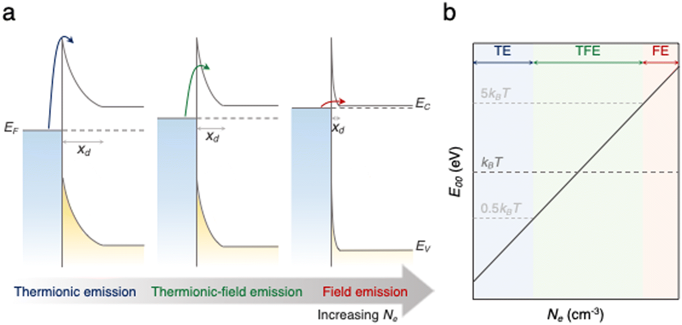 | ||
| Fig. 2 (a) Schematic representation of the carrier transport at the metal–semiconductor interface as doping concentration increases. (b) E00 as a function of doping density, illustrating the three charge injection modes: thermionic emission (TE) when E00 ≤ 0.5kT, thermionic-field emission (TFE) when 0.5kT < E00 < 5kT, and field emission (FE) when 5kT ≤ E00. | ||
2.3 Extraction method: the gated transmission line method
The RC in AOS TFTs is closely associated with the voltage required for charge transport across M–S interfaces at both the source-channel and channel-drain junctions. The applied voltage (Vapp) is distributed between the contact and channel regions, as expressed by the equation Vapp = 2ΔVSD + ΔVCh = ID(2RC + Rch) (Fig. 3(a)). Here, ΔVSD represents the voltage drop at the source and drain (S/D) and the channel interface, which primarily comes from the RC that results from the energy barrier impeding carrier injection at the M–S junction. Given the significant impact RC has on the electrical properties of AOS-based devices, accurate measurement of RC is essential for evaluating contact enhancement strategies (Section 3). | ||
| Fig. 3 (a) Schematic representation of a device illustrating the resistor network RT = Rch + 2RC, along with a voltage profile indicating the voltage drop across the drain–channel–source region. (b) Energy band diagram showing the barrier decreasing as VG increases, with a plot demonstrating the VG dependence of RC for high VG and low ΦB. (c), (d) Schematic graphs for a transmission line method (TLM) of RT as a function of L. | ||
Both Rch and RC exhibit gate bias (VG) dependency due to the shift in the Fermi level within the semiconductor and the gate-field-induced reduction of the barrier height and width at the M–S interface (Fig. 3(b)). To accurately characterize RC, the gated transmission line method (g-TLM), also known as the gated transfer length model, is commonly employed. This method analyzes current–voltage (I–V) characteristics at different gate voltages (VG ≫ VT) in the linear region (VD → 0) using a set of devices with varying channel lengths (L), resulting in a family of TLM curves. The I–V characteristics in the linear region are described by the equation:28
 | (1) |
 | (2) |
Taking RC into account, the total device resistance (RT) is given by:
 | (3) |
Because Rc remains constant while Rch varies linearly with L, plotting RT against L at a fixed VG yields a straight line. If no intersection occurs (Fig. 3(c)), ΔL = 0 and RC become dependent on VGS due to its correlation with carrier density. Here RC and Rsh, where Rch = RshL/W, can be extracted as a function of VG. Alternatively, if an intersection occurs, ΔL ≠ 0, the convergence point indicates 2ΔL and 2RC, in accordance with eqn (3). The value of ΔL generally arises from the diffusion of oxygen vacancies (VO), which is more pronounced in the OSs with a higher concentration of VO.43 This diffusion leads to a reduction in SB width, thereby facilitating carrier injection and rendering electron injection independent of VG.
3. Improvement method
When silicon is directly interfaced with metals, a Schottky junction forms due to Fermi level pinning, which arises from MIGS and the thermal instability caused by metal–silicon interdiffusion.44 To overcome this issue, a silicide coupling layer is often introduced at the interface, creating an ohmic contact that reduces RC while enhancing both the thermal and structural stability of the junction (Fig. 4(a)). Extensive research on improving the electrical contact properties of Si-based devices has focused on the use of different silicides, such as TiSi2, NiSi, and CoSi2, to optimize these properties.45–49 | ||
| Fig. 4 Schematic illustrations of (a) silicon and (b) OS transistors. A number of different silicides are used to decrease the contact resistance in silicon transistors. In OS transistors, several methods are used, such as formation of a conduction region or insertion of an interlayer between the OS and the source or drain. | ||
In indium-based OSs, such as a-IGZO, IZTO, and IGO, recent research efforts have focused on reducing the effective ΦB at the metal–OS interfaces. The indium-based channels generally have relatively high work functions, typically exceeding 4 eV.50–52 Despite efforts to pair these semiconductors with metals with similarly high ΦM, achieving a low ΦB remains a significant challenge. To overcome this, two primary approaches have been explored: (1) the formation of an n+-doped conduction region at the M–S interface, and (2) the insertion of interlayers (ILs) to modify the interface (Fig. 4(b)). The anticipated advantages and limitations of these methods are outlined in Table 1, with their corresponding electrical properties detailed in Table 2. A comprehensive discussion of both strategies is provided in the following section.
| Approach | Pros. | Cons. | |
|---|---|---|---|
| Conductive region formation | Metal-induced | No additional processing required | Formation of unwanted MOx interfacial layers |
| Doping | Broadly investigated | Deterioration of the OS surface | |
| Temporal instability | |||
| Limited process margin | |||
| OS engineering | No additional processing required | Alteration of overall electrical properties | |
| Interlayer insertion | n+ layer | Without deterioration of the OS surface | Requires additional processing steps |
| DB layer | Prevents intermixing at the interface | Limitation in further improvement |
| Approach | OS | Deposition method | W/L (μm) | R c W (Ω cm) | ρ C (Ω cm2) | μ FE (cm2 V−1 s−1) | Ref. |
|---|---|---|---|---|---|---|---|
| W/L: width and length of the channel; ρC: specific contact resistivity. | |||||||
| Metal-induced | IGZO | SPT | 16/8 | — | 5.2 × 10⁻⁴ | 16.1 | 53 |
| IGZO | SPT | 2.4/0.8 | 2.7 | — | 8.5 | 54 | |
| Doping | IGZO | SPT | 3/5 | 10.2 | — | 17.2 | 55 |
| IGZO | SPT | — | — | 1.3 × 10⁻⁶ | — | 56 | |
| ZnO | ALD | 15/2 | 0.3 | — | 39.2 | 57 | |
| IGZTO | SPT | 10/10 | 11.3 | — | 27.2 | 58 | |
| OS engineering | In2O3 | ALD | —/0.04 | 0.002 | 1.3 × 10⁻⁹ | — | 59 |
| IGZO | ALD | 24/24 | 1.8 | — | 36.9 | 60 | |
| n+ layer | IGZO | SPT | 300/500 | 510.0 | — | 12.0 | 61 |
| IGZO | ALD | 60/30 | 0.1 | 4.2 × 10⁻⁷ | 45.3 | 62 | |
| DB layer | IGZO | SPT | 625/95 | 18.0 | — | 11.5 | 63 |
| IGZO | SPT | 1000/150 | 104.5 | — | 14.8 | 64 | |
3.1. Conductive region formation
Al-induced method. In a study by Yang et al., self-aligned top-gate a-IGZO TFTs were fabricated, focusing on the Al-induced doping effect to create conductive S/D regions.65 Post-deposition annealing (PDA) at 200 °C after Al deposition significantly increased VO at the Al/a-IGZO interface. X-ray photoelectron spectroscopy (XPS) of the O1s spectra revealed an increase in VO from 27% to 58% after the 200 °C PDA. Additionally, a shift in the In 3d XPS peaks indicated the reduction of In according to the reaction: 2Al + In2O3 → Al2O3 + 2In (Gibbs free energy (ΔG) = −752.6 kJ mol−1). The resulting I–V characteristics of the Al-treated TFTs showed enhanced drain current in the on-state region, without current crowding at low VD, indicating good ohmic contact with a low RCW of 10 Ω cm, while the untreated TFTs exhibited significantly suppressed drain current (Fig. 5(a)).
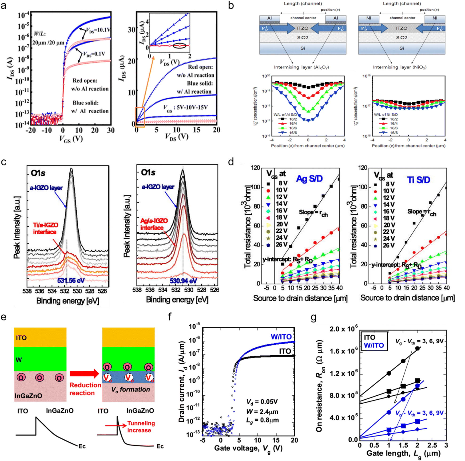 | ||
| Fig. 5 (a) The I–V characteristics with and without an Al reaction. (b) Schematic illustration comparing the diffusion extent of V+O when using Al and Ni electrodes (top images), along with a simulation of V+O concentration in the ITZO layer (bottom images). (c) O1s XPS analysis from Ti/a-IGZO and Ag/a-IGZO interfaces from the TFT devices. (d) RT plotted with respect to a-IGZO TFT channel length for different VG with Ag and Ti electrodes. (e) Schematic illustration of the interfacial reaction between W and IGZO. (f) ID–VG characteristics of IGZO TFTs using ITO and W/ITO. (g) On resistance of IGZO TFTs using ITO and W/ITO. | ||
However, the strong reducing power of Al can lead to excessive conductivity in the channel region, potentially degrading the transfer characteristics.66 Park et al. suggested that Ni electrodes would be more suitable S/D electrodes for high-density applications, where precise contact properties are crucial.53 Thermally deposited Ni and Al electrodes were compared in terms of contact performance (Fig. 5(b) images shown top). Technology computer-aid design simulations showed that the Ni electrodes exhibited superior electrical properties compared to the Al electrodes, which was attributed to two factors: (1) a reduced generation and diffusion of V+O, which acts as a shallow donor, and (2) a lower metal intermixing at the M–S junctions in Ni-based devices (Fig. 5(b) images shown below).
Ti-induced method. Ti, known for its strong reducing power, can generate VO and form TiO2 at the interface with indium-based channels.67 In a study by Choi et al., using Ti as S/D electrodes in a-IGZO TFTs significantly lowered the resistance compared to Ag S/D electrodes.68 Analysis with XPS revealed the formation of a TiOx layer and VO at the Ti/a-IGZO interface, facilitated by the lower formation enthalpy of TiOx compared to that of In2O3, Ga2O3, and ZnO (Fig. 5(c)). In contrast, no VO generation was observed at the Ag/a-IGZO interface, resulting in higher RC. Consequently, the specific contact resistivity (ρC) of the Ti electrode was approximately one-third that of the Ag electrodes (Fig. 5(d)). However, the use of Ti electrodes can lead to V+O formation and metal diffusion after thermal treatment, potentially reducing the effective channel length. This limits Ti's suitability for applications requiring aggressive scaling. Thus, Ti is often used in its metal–nitride form or combined with other materials.69
W-induced method. To mitigate the effective channel length shortening caused by VO and metal diffusion during high temperature annealing, Kataoka et al. explored the use of indium tin oxide (ITO), which exhibits lower reactivity with IGZO.54 However, the use of ITO alone resulted in a lower on-current compared to Ti electrodes due to a higher RC. To address this, a 2 nm thick W layer was introduced to form a W/ITO electrode. XPS depth profile analysis revealed W–O bonds at the W/IGZO interface, indicating the formation of WO3, which was absent in the W/ITO interface. Additionally, Ga 2p spectra indicated a reduction reaction between W and IGZO, leading to VO formation and thinning of the depletion layer, thereby increasing the tunneling current (Fig. 5(e) and (f)). The RCW values of the ITO and W/ITO were measured to be 1.8 × 10⁵ and 2.7 × 10⁴ Ω μm, respectively, with the W/ITO electrode exhibiting the lowest RC (Fig. 5(g)). Other studies have also investigated the use of metals with strong reducing power to form an n+ region at the OS interface while minimizing channel shortening.70,71
Ion implantation. Several studies have explored the formation of n+ regions using B ion implantation.72,73 Kang et al. investigated the effect of varying implantation energy during B+ ion implantation on the RC of self-aligned coplanar a-IGZO TFTs (Fig. 6(a)).55 B acts as an n-type dopant in metal oxide TFTs and is also well known for its stability at high temperature, due to the strong B–O bond. Ion implantation was performed at 30, 35, and 40 keV to compare the effects of implantation energy on device characteristics (Fig. 6(b)). With increasing implantation energy, device mobility improved and the RcW decreased. However, the lateral spread (ΔL) of the implanted ions increased, likely due to enhanced B ion diffusion at higher energies. The ΔG of B2O3 (−1,192.9 kJ mol−1) was significantly lower than that of In2O3 (−830.7 kJ mol−1), Ga2O3 (−998.3 kJ mol−1), and ZnO (−348.1 kJ mol−1), which facilitated the formation of stable B–O bonds. This stability, in conjunction with oxygen interstitials, led to the creation of VO sites during ion bombardment, ultimately increasing the carrier concentration (ne).
 | ||
| Fig. 6 (a) Schematic illustration of the reaction of B ions implanted in the IGZO surface. (b) The I–V characteristics at different B implantation energies. (c) Illustration of S/D series resistance Rch + RSD at the gate edges in TFTs. (d) Measurements of the S/D series resistances in Ne+ (left) or B+ (right) implanted TFTs as a function of gate length (Lg) for VG of 15, 17, and 20 V. | ||
Moreover, Ui et al. compared the effects of Ne+ and B+ ion implantation in a-IGZO TFTs.74 Although Ne+ ions are larger, they exhibited greater diffusion within a-IGZO during annealing, resulting in a smaller ΔL for B+ implantation (Fig. 6(c) and (d)). This behavior was attributed to the stronger B–O bonding, which restricted diffusion. These findings underscore the importance of considering ion size, bonding energy, and implantation energy when optimizing ion implantation for contact region doping. Other ions, such as F and N, have also been investigated for similar doping applications.75–77
Plasma treatment. Plasma treatment, particularly using H and Ar plasma, has been extensively studied as an effective method for lowering the RC in OS TFTs.78–84 In an investigation by Park et al., H plasma treatment with a variety of conditions was analyzed using TLM extraction to assess its impact on RC (Fig. 7(a)).56 The findings indicated that H treatment reduces the potential barrier width by increasing ne, although weak M–OH bonds are partially diffused during the process. It was observed that RC varied with plasma power and temperature, as shown in Fig. 8(b). The study emphasized that optimizing plasma power and process temperature is critical. Higher RF power introduces excessive H into a-IGZO, forming unstable bonds that lead to device instability. Proper thermal processing can mitigate this instability. Ahmad et al. investigated the relationship between ρC, hydrogen doping, and diffusion at the channel-S/D interface, noting changes in work function with increasing hydrogen plasma treatment time (Fig. 7(b)).85 However, the high diffusivity and reactivity of H imposed limitations on process temperature and conditions.86 Consequently, alternative approaches focused on inert gases, such as Ar and Ne, for plasma treatments.
 | ||
| Fig. 7 (a) Schematic illustration of hydrogen plasma treatment on TFTs (left) and ρC as a function of process temperature and plasma power. (b) The schematic energy diagram of the work function at the Mo/IGZO interface. (c) The energy band diagrams of a Ti electrode and an OS layer, before (left) and after (right) contact. The effective potential barrier width is reduced with an Ar plasma process. (d) Top-down and cross-section SEM images of TFT (left) and the transfer characteristics of TFTs with and without Ar plasma treatment. (e) The illustration of the different mechanisms of Ar+ and N+ plasma treatments. (f) Width-normalized RT as a function L for TFTs fabricated with Ar (left) and N (right) plasma treatment. (g) Model of F doping showing VO passivated by F or F substitution for O. When F concentration increases, resistivity decreases. | ||
 | ||
| Fig. 8 (a) Schematic of the energy band diagram for contact structures of ITO and IGZO with low In concentration (left) and high In concentration (right). (b) Linear fit obtained from the TLM analysis for low In concentration (device A) and high In concentration (device B). (c) Schematic of the band diagram of IGZO and IZO. (d) Comparison of S/D RC between IZO FETs and IGZO FETs. (e) Channel thickness dependence of ρC and current transfer length (left), and transfer characteristics for different channel thicknesses (right). (f) ρC with channel thicknesses (TITO) of 5 and 10 nm (left) and RSD for different TITO (right). | ||
In the work by Lu et al., Ar plasma treatment was shown to affect contact properties, with prolonged treatment time promoting VO formation, thereby reducing the barrier width, enhancing tunneling, and subsequently decreasing RC (Fig. 7(c)).57 This impact was significant in short-channel devices. For example, Zhang et al. demonstrated effective RC reduction in a 302 nm self-aligned bottom-gate a-IGZO TFT, and attributed the improvement to increased VO and carrier density (Fig. 7(d)).87 The improved I–V transfer characteristics showed enhanced on-current and notable reliability, indicating that Ar plasma treatment is a promising technique for nanoscale AOS technologies, including micro-displays, flexible integrated circuits, and advanced optoelectronic applications.
Due to the relatively large mass of Ar ions, which can etch OS films, treatment with a nitrogen (N) plasma has also been investigated as a lower impact alternative.58 The N plasma treatment has resulted in reduced RCW and ΔL compared to an Ar plasma, which could be attributed to N's smaller ion mass and reduced collateral effects (Fig. 7(e) and (f)). Additionally, F plasma treatment has been explored as a technique to reduce RC.88,89 F ions, due to their similar ion radius to O, effectively passivate VO sites (Fig. 7(g)). The robust metal–F bonds exhibit higher bond energy than metal–O bonds, maintaining enhanced stability even after annealing at 600 °C. Furthermore, the influence of a mixture of gases, such as CF4 + O2 or Ar + O2, on RC has also been investigated, providing additional feasibility for the use of plasma treatments to optimize device performance.90–92
In a complementary study, Saito et al. found that IZO exhibited superior mobility and lower RC than IGZO TFTs.59 A measurement of ΦB based on a TE model indicated an ΦB of 0.46 eV for IGZO and 0.37 eV for IZO, highlighting a lower barrier in IZO. Moreover, Fowler–Nordheim tunneling current models revealed a 0.13 eV larger band offset at the IZO/SiO2 interface compared to IGZO, consistent with the ΦB difference (Fig. 8(c)). These findings underscored the critical role of metal composition in modulating ΦB and RC, with IZO TFTs showing approximately 75% lower S/D resistance compared to IGZO TFTs (Fig. 8(d)).
Channel thickness also influences carrier density, which in turn affects RC. Niu et al. have observed that increasing carrier density in In2O3 results in ρC (Fig. 8(e)), and have proposed an optimal channel thickness for achieving target carrier density essential for next-generation, high-performance ultra-scaled back end of the line electronics.60 However, while higher carrier density can decrease RC, it may shift the material's behavior toward metallicity, necessitating careful optimization to balance a low RC with semiconducting properties (Fig. 8(f)).96
As channel dimensions scale downward, thermal electron injection over the SB can lead to a significant increase in RC. Recent research has therefore focused on optimizing channel thickness to modulate carrier density and exploring structural modifications to improve contact properties, with the ultimate goal of developing TFTs that combine high on-current and stable VT.97,98
3.2. Interlayer insertion
Homogeneous layer. The ne in sputter-derived OS layers can be modulated by controlling the oxygen partial pressure (PO2), power, and cation composition during the deposition process. Kim et al. investigated the modulation of the contact barrier in a-IGZO TFTs by varying the PO2 in a homogenous IL, as shown in Fig. 9(a).61 The deposition ratio of O2/(O2 + Ar) was adjusted to 1% (type 1), 0% (type 2), and 20% (type 3) for the sputtered a-IGZO IL, using the same target as the channel layer. The type 2 device exhibited an improved μFE of 12.03 cm2 V−1 s−1, a negative VT shift of −4.1 V, and a 2.3-fold reduction in RCW compared to the type 1 device, which had a μFE of 9.95 cm2 V−1 s−1, a VT of 5.8 V, and an RCW of 575 Ω cm (Fig. 9(c) and (d)). The increase in PO2 from 0% to 1% and 20% resulted in a significant reduction in VO from 39.1% to 21.9% and 12.6%, respectively, driven by the reaction 1/2O2 + V2+O + 2e− → OO (Fig. 9(b)). Consequently, the higher ne observed in the type 2 IGZO IL can be attributed to the presence of intrinsic VO defects, which act as donors and effectively form a highly doped layer, thereby enhancing ohmic contact properties.
 | ||
| Fig. 9 (a) Energy band alignment of the contact region for a-IGZO TFTs without an interlayer (IL) and with a low resistivity IL. (b) O 1s XPS spectra of IGZO thin films with oxygen ratios of 0% and 1% during deposition. (c) RTW as a function of L for three device types: type 1 without an IL; type 2 with an n+-IGZO IL; type 3 with an n−-IGZO IL. (d) Transfer characteristics of the three a-IGZO TFT types. (e) Contact scheme-dependent ρC and RCW in a-IGZO TFTs with different ILs. (f) Hall effect measurements of the IGTO/IGZO thin-film stacks with IGTO thickness (tIGTO) values of 0, 5, 8, and 12 nm. (g) GIXRD pattern of the IGTO thin films with varying tIGTO. (h) Device schematic of the proposed a-IGZO TFT structure with a cross-sectional HRTEM image. (i) RT–L plots as a function of VG in a-IGZO TLM devices with different ILs. (j) Schematic energy band diagrams at the contact region. (k) Transfer characteristics at VD of 0.1 V with different ILs. | ||
Heterogeneous layer. Many studies have focused on identifying the optimal conditions for IL to achieve superior electrical contact properties. Recently, Jeong et al. proposed a multi-stack IL structure composed of an oxygen-scavenging TiN layer and an n+ IGTO layer, highlighting the thickness dependence of the IGTO layer (tIGTO) on the RC of a-IGZO devices.103 IGZO TFTs with a TiN/IGTO (3/8 nm) IL had the lowest RCW of 0.7 Ω cm, which was significantly lower than the control device, which had an RCW of 6.9 Ω cm. The observed performance degradation when tIGTO > 8 nm, as shown in Fig. 6(e), was attributed to changes in crystallinity. Despite the high ne in 12 nm thick IGTO (Fig. 9(f)), crystallization-induced deterioration at the M–S interface caused an increase in RCW to 1.3 Ω cm. Additionally, Jeong et al. reported on an ALD-based ultrathin IL method (Fig. 9(h)).62 The optimized doping ratio of an Al-doped ZnO IL was achieved by adjusting the number of Al2O3 injection cycles during the ALD process, resulting in the lowest RCW of 0.13 Ω cm at an Al2O3
![[thin space (1/6-em)]](https://www.rsc.org/images/entities/char_2009.gif) :ZnO ratio of 2:8 (Fig. 9(i)). This substantial improvement was corroborated by a schematic energy band diagram, based on UPS and ellipsometry analysis, which indicated a reduction in ΦB due to the IL's high ne. This enhanced electrical contact contributed to an increase in μFE from 38.8 to 45.3 cm2 V−1 s−1, as shown in Fig. 9(k).
:ZnO ratio of 2:8 (Fig. 9(i)). This substantial improvement was corroborated by a schematic energy band diagram, based on UPS and ellipsometry analysis, which indicated a reduction in ΦB due to the IL's high ne. This enhanced electrical contact contributed to an increase in μFE from 38.8 to 45.3 cm2 V−1 s−1, as shown in Fig. 9(k).
 | ||
| Fig. 10 (a) Transfer and output characteristics of a-IGZO TFTs with different S/D electrodes: Cu, CuCa, and CuCa/CuCaOx. (b) Elemental depth profiling results for the a-IGZO devices with different S/D electrodes. (c) Cross-sectional TEM images of the channel and electrode stacks. (d) Concept of the synergistic effect in Cu/MoTi/IGZO stacks, combining diffusion blocking against Cu migration and forming a good n+ layer. (e) Cross-sectional TEM images of Cu/IGZO, Cu/Mo/IGZO, Cu/Ti/IGZO, and Cu/MoTi/IGZO stacks. (f) Elemental depth profiles from EDS analysis of Cu and O for different stacks. | ||
4. Suggestion
As the semiconductor industry progresses toward higher integration for PPAC, reducing device dimensions has become essential. This has spurred interest in short-channel and 3D structures such as VCTs, gate-all-around (GAA), and channel-all around (CAA) designs. However, research aimed at minimizing ΔL to mitigate SCEs while suppressing performance degradation caused by RC remains relatively limited. To enable the application of OS in 3D architectures, further investigations into RC reduction strategies and geometrical effects on RC are imperative. Contact geometry plays a pivotal role in influencing local current density through variations in the electric field. While electric field concentration near edge contact can enhance charge transport and reduce RC, it can also cause localized temperature rises along the current paths, resulting in increased RC.105,106 Therefore, optimizing contact geometry to manage field concentration is essential for improving device performance. In this context, studies have explored strategies to mitigate current crowding effects on RC by modulating contract area and channel edge design. For instance, in transition-metal dichalcogenides (TMDs), minimized contact areas are often employed, whereas OSs have been investigated with an emphasis on increasing contact areas.107–111 Specifically, integrating OS into DRAM architectures with nanometer-scale contact holes (∼1 × 10⁻¹² cm2) requires achieving a specific contact resistivity (ρC = RC·AC) below 10−6 Ω cm2 to avoid performance degradation and ensure reliable device operation. Meeting this target necessitates further research into scaling-friendly contact engineering approaches tailored to ultra-scaled and 3D device architectures.5. Conclusion
OSs are emerging as promising candidates for next-generation channel materials, with the potential to address the scaling limitations inherent in conventional silicon-based devices. This review focuses on key strategies for reducing RC in OS-based TFTs, which remains a critical challenge for further miniaturization and performance enhancement. While various methods – such as conductive region formation and interlayer insertion – have been explored to reduce RC in OS TFTs, the majority of studies have focused on devices with relatively long channel length (>1 μm). The effectiveness of these strategies for sub-micrometer or even sub-100-nanometer channel lengths is highly dependent on the fabrication process, structure, and thermal budget. This remains an open question and warrants further investigation. In particular, the formation of an n+ conduction region and interlayer insertion have demonstrated effectiveness in lowering the effective potential barrier between metal and semiconductor and enhancing carrier injection. As OS technologies advance into more sophisticated applications, such as DRAM, reducing RC will be vital to meet the performance demands of future semiconductor devices. Continued innovation in contact engineering will be vital for unlocking the full potential of OSs in high-performance, scalable electronics, paving the way for their integration into future device architectures.Data availability
The datasets used and/or analyzed during the current study are available from the corresponding author on reasonable request.Conflicts of interest
There are no conflicts to declare.Acknowledgements
This work was supported by the National Research Foundation (NRF) grant funded by the Korean government (NRF-2022M3H4A6A01035636, and 2022M3H4A1A04068923) and Samsung Electronics Co., Ltd (IO240814-10715-01, and IO201210-08034-01).References
- K. Nomura, H. Ohta, A. Takagi, T. Kamiya, M. Hirano and H. Hosono, Nature, 2004, 432, 488–492 CrossRef CAS PubMed
.
- T. Kim, C. H. Choi, J. S. Hur, D. Ha, B. J. Kuh, Y. Kim, M. H. Cho, S. Kim and J. K. Jeong, Adv. Mater., 2023, 35, 2204663 CrossRef CAS PubMed
- J. F. Wager, Inf. Disp., 2016, 32, 16–21 Search PubMed
- T. Kamiya and H. Hosono, NPG Asia Mater., 2010, 2, 15–22 CrossRef
- H. Hosono, Nat. Electron, 2018, 1, 428 CrossRef
- B. He, G. He, L. Zhu, J. Cui, E. Fortunato and R. Martins, Adv. Funct. Mater., 2024, 34, 2310264 CrossRef CAS
- J. E. Yang, Y. Jang, N. R. Han, H. J. Sung, J. K. Kim, Y. Cha, K. H. Lee, K. Jung, M. Jung, W. Lee, M. H. Cho and S. Kim, 2024 IEEE Symposium on VLSI Technology and Circuits (VLSI, Technology and Circuits), 2024, pp. 1–2, DOI:10.1109/VLSITechnologyandCir46783.2024.10631550.
- D. Ha, W. Lee, M. H. Cho, M. Terai, S. W. Yoo, H. Kim, Y. Lee, S. Uhm, M. Ryum, C. Sung, Y. Song, K. Lee, S. W. Park, K. S. Lee, Y. S. Tak, E. Hwang, J. Chea, C. Im, S. Byeon, M. Hong, K. Sim, W. J. Jung, H. Ryu, M. J. Hong, S. Park, J. Park, Y. Choi, S. Lee, G. Woo, J. Lee, D. S. Kim, B. J. Kuhm, Y. G. Shin and J. Song, 2023 International Electron Devices Meeting (IEDM), IEEE, 2023, pp. 1–4.
- A. Belmonte, H. Oh, N. Rassoul, G. L. Donadio, J. Mitard, H. Dekkers, R. Delhougne, S. Subhechha, A. Chasin, M. J. van Setten, L. Kljucar, M. Mao, H. Puliyalil, M. Pak, L. Teugels, D. Tsvetanova, K. Banerjee, L. Souriau, Z. Tokei, L. Goux and G. S. Kar, 2020 IEEE International Electron Devices Meeting (IEDM), 2020, p. 28 Search PubMed.
- S. Ryu, M. Kang and S. Kim, Adv. Mater. Technol., 2024, 9, 2302209 CrossRef CAS
- A. R. Choi, D. H. Lim, S. Y. Shin, H. J. Kang, D. Kim, J. Y. Kim, Y. Ahn, S. W. Ryu and I. K. Oh, Chem. Mater., 2024, 36, 2194–2219 CrossRef CAS
- J. S. Hur, S. Lee, J. Moon, H. G. Jung, J. Jeon, S. H. Yoon, J. H. Park and J. K. Jeong, Nanoscale Horiz., 2024, 9, 934–945 RSC
- J. C. Chiu, E. Sarkar, Y. M. Liu, Y. C. Chen, Y. C. Fan and C. W. Liu, 2023 IEEE Symposium on VLSI Technology and Circuits (VLSI, Technology and Circuits), 2023, pp. 1–2.
- Q. Li, W. Zhao, Q. Hu, C. Gu, S. Zhu, H. Liu, R. Huang and Y. Wu, 2023 International Electron Devices Meeting (IEDM), 2023, pp. 1–4 Search PubMed.
- S. Jeon, K. H. Lee, S. H. Lee, S. I. Cho, C. S. Hwang, J. B. Ko and S. H. K. Park, J. Mater. Chem. C, 2023, 11, 14177–14186 RSC
- J. Raja, K. Jang, C. P. T. Nhuyen, N. Balaji, S. Chatterjee and J. Yi, IEEE Electron Device Lett., 2014, 35, 756–758 CAS
- J. Lee, S. Byeon, S. Kim, S. W. Yoo, W. Lee, S. Hong, M. H. Cho, S. J. Kim, D. Ha and D. S. Kim, IEEE Electron Device Lett., 2024, 45, 1655–1668 Search PubMed
- P. Barquinha, A. M. Vilà, G. Gonçalves, L. Pereira, R. Martins, J. R. Morante and E. Fortunato, IEEE Trans. Electron Devices, 2008, 55, 954–960 CAS
- H. Tang, A. Dayeh, S. T. Picraux, J. Y. Huang, and K. N. Tu, Nano Lett., 2012, 12, 3979–3985 CrossRef PubMed
- H. Tang, H. Dekkers, N. Rassoul, S. Sutar, S. Subhechha, V. Afanas’ev, J. Van Houdt, R. Delhougne, G. S. Kar and A. Belmonte, IEEE Trans. Electron Devices, 2024, 71, 567–573 CAS
- Z. Wu, J. Niu, C. Lu, Z. Bai, K. Chen, Z. Wu, W. Lu, M. Liu, F. Liao, D. Geng, N. Lu, G. Yang and L. Li, IEEE Electron Device Lett., 2024, 45, 408–411 CAS
- S. Lee and A. Nathan, Science, 2016, 354, 302–304 CrossRef CAS PubMed
- A. Barua, K. D. Leedy and R. Jha, Solid State Electron. Lett., 2020, 2, 59–66 CrossRef
- M. H. Cho, M. J. Kim, H. Seul, P. S. Yun, J. U. Bae, K. S. Park and J. K. Jeong, J. Inf. Disp., 2019, 20, 73–80 CrossRef CAS
- E. Fortunato, P. Barquinha and R. Martins, Adv. Mater., 2012, 24, 2945–5986 CrossRef CAS
- A. Olziersky, P. Barquinha, A. Vilà, C. Magaña, E. Fortunato, J. R. Morante and R. Martins, Mater. Chem. Phys., 2011, 131, 512–518 CrossRef CAS
- P. Barquinha, L. Pereira, G. Gonçalves, R. Martins and E. Fortunato, Electrochem. Solid-State Lett., 2008, 11, 248–251 CrossRef
-
B. G. Streetman and S. Banerjee, Solid State Electronic Devices, 2000, vol. 4 Search PubMed
-
S. M. Sze, Y. Li and K. K. Ng, Physics of semiconductor devices, John wiley & sons, 2021 Search PubMed
- L. J. Brillson, Y. Dong, F. Tuomisto, B. G. Svensson, A. Y. Kuznetsov, D. Doutt, H. L. Mosbacker, G. Cantwell, J. Zhang, J. J. Song, Z. Q. Fang and D. C. Look, J. Vac. Sci. Technol., B, 2012, 30, 050801 CrossRef
- S. Yogev, R. Matsubara, M. Nakamura, U. Zschieschang, H. Klauk and Y. Rosenwaks, Phys. Rev. Lett., 2013, 110, 036803 CrossRef CAS PubMed
- L. J. Brillson, J. Vac. Sci. Technol., A, 2007, 25, 943–949 CrossRef CAS
- J. Robertson, J. Vac. Sci. Technol., A, 2013, 31, 050821 CrossRef
- J. Tersoff, Phys. Rev. Lett., 1984, 52, 465 CrossRef CAS
- J. Robertson and L. Lin, Microelectron. Eng., 2011, 88, 373–376 CrossRef CAS
- T. Nishimura, K. Kita and A. Toriumi, Appl. Phys. Lett., 2007, 91, 123123 CrossRef
- S. Kurtin, T. C. McGill and C. A. Mead, Phys. Rev. Lett., 1969, 22, 1433 Search PubMed
- M. Lorenz, A. Lajn, H. Frenzel, M. Grundmann, P. Barquinha, R. Martins and E. Fortunato, Appl. Phys. Lett., 2010, 97, 243506 CrossRef
- H. Frenzel, A. Lajn, M. Brandt, H. V. Wenckstern, G. Biehne, H. Hochmuth, M. Lorenz and M. Grundmann, Appl. Phys. Lett., 2008, 92, 192108 CrossRef
- H. Frenzel, A. Lajn, H. V. Wenckstern, G. Biehne, H. Hochmuth and M. Grundmann, Thin Solid Films, 2009, 518, 1119–1123 CrossRef CAS
-
D. K. Schroder, Semiconductor Material and Device Characterization, John Wiley & Sons, 2015, 978-0-471-73906-7 Search PubMed
- J. G. J. Chern, P. Chang, R. F. Motta and N. Godinho, IEEE Electron Device Lett., 1980, 1, 170–173 Search PubMed
- N. On, B. K. Kim, S. Lee, E. H. Kim, J. H. Lim and J. K. Jeong, IEEE Trans. Electron Devices, 2020, 67, 5544–5551 CAS
- L. Lin, Y. Guo and J. Robertson, Appl. Phys. Lett., 2012, 101, 052110 CrossRef
- M. S. Kim, S. H. Hwang, S. H. Kim, J. H. Kim, E. Park, K. H. Han and H. Y. Yu, IEEE Electron Device Lett., 2023, 44, 1040–1043 CAS
- H. Jeon, B. Jung, Y. D. Kim, W. Yang and R. J. Nemanich, J. Appl. Phys., 2000, 88, 2467–2471 CrossRef CAS
- A. Newman, A. Campos, D. Pujol, P. Fornara, M. Gregoire and D. Mangelinck, Mater. Sci. Semicond. Process., 2023, 162, 107488 CrossRef CAS
- W. Tang, S. T. Picraux, J. Y. Huang, A. M. Gusak, K.-N. Tu and S. A. Dayeh, Nano Lett., 2013, 13, 2748–2753 CrossRef CAS PubMed
- X. Chen, F. Du, C. Wang, H. Xu, Y. Zhang, F. Hou, X. Yang, Y. Wu, C. Tsai, Z. Chen, Y. Guo, Z. Liu and X. Wu, IEEE Trans. Electron Devices, 2021, 68, 1378–1381 CAS
- M. H. Cho, C. H. Choi, M. J. Kim, J. S. Hur, T. Kim and J. K. Jeong, ACS Appl. Mater. Interfaces, 2023, 15, 19137–19151 CrossRef CAS PubMed
- H. J. Yang, H. J. Seul, M. J. Kim, Y. Kim, H. C. Cho, M. H. Cho, Y. H. Song, H. Yang and J. K. Jeong, ACS Appl. Mater. Interfaces, 2020, 12, 52937–52951 CrossRef CAS PubMed
- H. J. Seul, J. H. Cho, J. S. Hur, M. H. Cho, M. H. Cho, M. T. Ryu and J. K. Jeong, J. Alloys Compd., 2022, 903, 163876 CrossRef CAS
- J. Park, M. Shin and J. Yi, Mater. Sci. Semicond. Process., 2020, 120, 105253 CrossRef CAS
- J. Kataoka, N. Saito, T. Ueda, T. Tezuka, T. Sawabe and K. Ikeda, Jpn. J. Appl. Phys., 2019, 58, SBBJ03 CrossRef CAS
- S. H. Kang, I. S. Lee, K. Kwak, K. T. Min, N. B. Choi, H. W. Hwang, H. C. Choi and H. J. Kim, ACS Appl. Electron. Mater., 2022, 4, 2372–2379 CrossRef CAS
- H. Park, J. Yun, S. Park, I. Ahn, G. Shin, S. Seong, H. J. Song and Y. Chung, ACS Appl. Electron. Mater., 2022, 4, 1769–1775 Search PubMed
- J. Lu, W. Wang, J. Liang, J. Lan, L. Lin, F. Zhou, K. Chen, G. Zhang, M. Shen and Y. Li, IEEE Electron Device Lett., 2022, 43, 890–893 CAS
- H. Tsuji, T. Takei, M. Ochi, M. Miyakawa, K. Nishiyama, Y. Nakajima and M. Nakata, IEEE J. Electron Devices Soc., 2022, 10, 229–234 CAS
- C. Niu, Z. Lin, V. Askarpour, Z. Zhang, P. Tan, M. Si, Z. Shang, Y. Zhang, H. Wang, M. S. Lundstrom, J. Maassen and P. D. Ye, IEEE Trans. Electron Devices, 2024, 71, 3403–3410 CAS
- D. H. Lee, Y. H. Kwon, N. J. Seong, K. J. Choi, G. Kim and S. M. Yoon, ACS Appl. Electron. Mater., 2022, 4, 6215–6228 CrossRef CAS
- T. Kim, Y. Kim, J. Ahn and E. K. Kim, ACS Appl. Electron. Mater., 2023, 5, 3772–3779 CrossRef CAS
- J. H. Jeong, S. H. Yoon, S. H. Lee, B. J. Kuh, T. Kim and J. K. Jeong, IEEE Electron Device Lett., 2024, 45, 849–852 CAS
- S. Hu, K. Lu, H. Ning, Z. Fang, X. Liu and W. Xie, IEEE Electron Device Lett., 2018, 39, 504–507 CAS
- J. L. Kim, C. K. Lee, M. J. Kim, S. H. Lee and J. K. Jeong, Thin Solid Films, 2021, 731, 138759 CrossRef CAS
- H. Yang, X. Zhou, H. Fu, B. Chang, Y. Min, H. Peng, L. Lu and S. Zhang, ACS Appl. Mater. Interfaces, 2021, 13, 11442–11448 CrossRef CAS PubMed
- T. Mudgal, N. Walsh, R. G. Manley and K. D. Hirschman, ECS Trans., 2014, 61, 405–417 CrossRef CAS
- H. Ji, A. Y. Hwang, C. K. Lee, P. S. Yun, J. U. Bae, K.-S. Park and J. K. Jeong, IEEE Trans. Electron Devices, 2015, 62, 1195–1199 CAS
- K.-H. Choi and H.-K. Kim, Appl. Phys. Lett., 2013, 102, 052103 CrossRef
- J. Lee, S. Byeon, S. Kim, S. W. Yoo, W. Lee, S. Hong, M. Hee Cho, S. Jin Kim, D. Ha and D. Sin Kim, IEEE Electron Device Lett., 2024, 45, 1665–1668 CAS
- Y. B. Li and T. P. Chen, ECS J. Solid State Sci. Technol., 2023, 12, 095003 CrossRef CAS
- D. Luo, H. Xu, M. Zhao, M. Li, M. Xu, J. Zou, H. Tao, L. Wang and J. Peng, ACS Appl. Mater. Interfaces, 2015, 7, 3633–3640 CrossRef CAS PubMed
- R. R. Chowdhury, M. S. Kabir, R. G. Manley and K. D. Hirschman, ECS Trans., 2019, 92, 135–142 CrossRef CAS
- M. S. Kabir, R. R. Chowdhury, R. G. Manley and K. D. Hirschman, ECS Trans., 2020, 98, 81–88 CrossRef CAS
- T. Ui, K. Yasuta, Y. Yamane and J. Tatemichi, ECS Trans., 2022, 109, 67–78 CrossRef CAS
- L. X. Qian, W. M. Tang and P. T. Lai, ECS Solid State Lett., 2014, 3, 87–90 CrossRef
- B. H. Lee, D. Y. Lee, J. Y. Lee, S. Park, S. Kim and S. Y. Lee, Solid-State Electron., 2019, 158, 59–63 CrossRef CAS
- S. H. Moon, Y. H. Kwon, N. J. Seong, K. J. Choi and S. M. Yoon, IEEE Electron Device Lett., 2023, 44, 1128–1131 CAS
- Y. Magari, H. Makino and M. Furuta, ECS J. Solid State Sci. Technol., 2017, 6, Q101–Q107 CrossRef CAS
- B. Du Ahn, H. S. Shin, H. J. Kim, J. S. Park and J. K. Jeong, Appl. Phys. Lett., 2008, 93, 203506 CrossRef
- X. D. Huang, J. Q. Song and P. T. Lai, IEEE Electron Device Lett., 2016, 37, 1574–1577 CAS
- J. S. Park, J. K. Jeong, Y. G. Mo, H. D. Kim and S. I. Kim, Appl. Phys. Lett., 2007, 90, 262106 CrossRef
- S. H. Yang, J. Y. Kim, M. J. Park, K. H. Choi, J. S. Kwak, H. K. Kim and J. M. Lee, Surf. Coat. Technol., 2012, 206, 5067–5071 CrossRef CAS
- J. H. Kang, E. Namkyu Cho, C. Eun Kim, M. J. Lee, S. Jeong Lee, J. M. Myoung and I. Yun, Appl. Phys. Lett., 2013, 102, 222103 CrossRef
- J. K. Lee, S. An and S. Y. Lee, IEEE Electron Device Lett., 2023, 44, 1845–1848 CAS
- D. Ahmad, J. Xu, J. Luo, N. Zhou, J. Gao and Y. Lu, Appl. Surf. Sci., 2024, 672, 160891 CrossRef CAS
- H. Jeong, B. Lee, Y. Lee, J. Lee, M. Yang, I. Kang, M. Mativenga and J. Jang, Appl. Phys. Lett., 2014, 104, 022115 CrossRef
- Y. Zhang, J. Li, Y. Zhang, H. Yang, Y. Guan, M. Chan, L. Lu and S. Zhang, IEEE Electron Device Lett., 2023, 44, 1300–1303 CAS
- J. G. Um and J. Jang, Appl. Phys. Lett., 2018, 112, 162104 CrossRef
- J. K. Um, S. Lee, S. Jin, M. Mativenga, S. Y. Oh, C. H. Lee and J. Jang, IEEE Trans. Electron Devices, 2015, 62, 2212–2218 Search PubMed
- H. Jang, S. J. Lee, Y. Porte and J. M. Myoung, Semicond. Sci. Technol., 2018, 33, 035011 CrossRef
- S. Knobelspies, A. Takabayashi, A. Daus, G. Cantarella, N. Münzenrieder and G. Tröster, Solid-State Electron., 2018, 150, 23–27 CrossRef CAS
- W. S. Liu, C. H. Hsu, Y. Jiang, Y. C. Lai and H. C. Kuo, Semicond. Sci. Technol., 2021, 36, 045007 CrossRef CAS
- J. W. Kim, T. J. Jung and S. M. Yoon, J. Alloys Compd., 2019, 771, 658–663 CrossRef CAS
- S. H. Bae, H. J. Ryoo, J. H. Yang, Y. H. Kim, C. S. Hwang and S. M. Yoon, IEEE Trans. Electron Devices, 2021, 68, 6159–6165 CAS
- N. Saito, T. Sawabe, J. Kataoka, T. Ueda, T. Tezuka and K. Ikeda, Jpn. J. Appl. Phys., 2019, 58, SBBJ07 CrossRef CAS
- Y. Kang, K. Han, Y. Chen and X. Gong, 2023 IEEE Symposium on VLSI Technology and Circuits (VLSI Technology and Circuits). IEEE, 2023, 1–2.
- S. H. Noh, H. E. Kim, J. H. Yang, Y. H. Kim, Y. H. Kwon, N. J. Seong, C. S. Hwang, K. J. Choi and S. M. Yoon, IEEE Trans. Electron Devices, 2022, 69, 5542–5548 CAS
- J. Zhang, Z. Lin, Z. Zhang, K. Xu, H. Dou, B. Yang, A. Charnas, D. Zheng, X. Zhang, H. Wang and P. D. Ye, IEEE Trans. Electron Devices, 2023, 70, 6651–6657 CAS
- C. Hung, S. Wang, C. Lin, C. Wu, Y. Chen, P. Liu, Y. Tu and T. Lin, Jpn. J. Appl. Phys., 2016, 55, 06GG05 CrossRef
- M. Liu, H. Kim, X. Wang, H. W. Song, K. No and S. Lee, ACS Appl. Electron. Mater., 2021, 3, 2703–2711 CrossRef CAS
- S. Choi, IEEE Electron Device Lett., 2020, 42, 168–171 Search PubMed
- Q. Li, C. Gu, S. Zhu, Q. Hu, W. Zhao and X. Li, IEDM, 2022, 2–7.
- J. H. Jeong, S. W. Seo, D. Kim, S. H. Yoon, S. H. Lee, B. J. Kuh, T. Kim and J. K. Jeong, Sci. Rep., 2024, 14, 10953 CrossRef CAS PubMed
- C. K. Lee, D. Y. In, D. J. Oh, S. H. Lee, J. W. Lee and J. K. Jeong, IEEE Trans. Electron Devices, 2018, 65, 1383–1390 CAS
- V. P. Madangarli, G. Gradinaru, G. Korony, T. S. Sudarshan, G. M. Loubriel, F. J. Zutavern and P. E. Patterson, Sandia National Labs, 1994, https://www.osti.gov/servlets/purl/10163562..
- V. P. Madangarli, G. Korony, G. Gradinaru and T. S. Sudarshan, IEEE Trans. Electron Devices, 1996, 43, 793–799 CrossRef CAS
- J. T. Smith, A. D. Franklin, D. B. Farmer and C. D. Dimitrako-poulos, ACS Nano, 2013, 7, 3661–3667 CrossRef CAS PubMed
- H. Y. Park, W. S. Jung, D. H. Kang, J. Jeon, G. Yoo, Y. Park, J. Lee, Y. H. Jang, J. Lee, S. Park, H. Y. Yu, B. Shin, S. Lee and J. H. Park, Adv. Mater., 2015, 28, 864–870 CrossRef PubMed
- V. Passi, A. Gahoi, E. G. Marin, T. Cusati, A. Fortunelli, G. Iannaccone, G. Fiori and M. C. Lemme, Adv. Mater. Interfaces, 2019, 6, 1801285 CrossRef
- W. Park, S. F. Shaikh, J. W. Min, S. K. Lee, B. H. Lee and M. M. Hussain, Nanotechnology, 2018, 29, 325202 CrossRef PubMed
- J. S. Kim, M. K. Joo, M. X. Piao, S. E. Ahn, Y. H. Choi, J. Na, M. Shin, M. J. Han, H. K. Jang and G. T. Kim, Thin Solid Films, 2014, 558, 279–282 CrossRef CAS
Footnote |
| † J. H. Jeong and J. E. Oh contributed to this work equally. |
| This journal is © The Royal Society of Chemistry 2025 |