 Open Access Article
Creative Commons Attribution 3.0 Unported Licence
n-Type doped transparent conducting binary oxides: an overview
Sebastian C.
Dixon
a,
David O.
Scanlon
bc,
Claire J.
Carmalt
a and
Ivan P.
Parkin
*a
aMaterials Chemistry Research Centre, Department of Chemistry, University College London, 20 Gordon Street, London WC1H 0AJ, UK. E-mail: i.p.parkin@ucl.ac.uk; Fax: +44 (0)20 7679 7463; Tel: +44 (0)20 7679 4669
bKathleen Lonsdale Materials Chemistry, Department of Chemistry, University College London, 20 Gordon Street, London WC1H 0AJ, UK
cDiamond House, Harwell Science and Innovation Campus, Diamond Light Source Ltd., Didcot, Oxfordshire OX11 0DE, UK
First published on 29th June 2016
Abstract
This article focuses on n-type doped transparent conducting binary oxides – namely, those with the general formula MxOy:D, where MxOy is the host oxide material and D is the dopant element. Such materials are of great industrial importance in modern materials chemistry. In particular, there is a focus on the search for alternatives to indium-based materials, prompted by indium's problematic supply risk as well as a number of functional factors. The important relationship between computational study and experimental observation is explored, and an extensive comparison is made between the electrical properties of a number of the most interesting experimentally-prepared materials. In writing this article, we aim to provide both an accessible tutorial of the physical descriptions of transparent conducting oxides, and an up-to-date overview of the field, with a brief history, some key accomplishments from the past few decades, the current state of the field as well as postulation on some likely future developments.
1 Introduction
1.1 Transparent conducting oxides
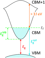
TCOs have been developed to sidestep this conundrum by doping the material in order to facilitate the creation of charge carriers. In a more sophisticated description of the band model, there is an important distinction between the fundamental band gap such as that described above (i.e. the energy separation of the bulk HOMO and LUMO), and the optical band gap, which corresponds to the lowest-energy allowed optical transition. For a TCO to be useful, it is this optical band gap which becomes important for the transparency of the material, which means that in an n-type TCO, electrons can be injected from a nearby defect donor level directly into the conduction band in order to permit conductivity. In n-type TCOs, lattice defects in a metal oxide crystal, such as oxygen vacancies, proton interstitials and certain substitutional defects, effectively create an excess of electrons close to the defect site. If there is sufficient orbital overlap, it permits delocalisation of electrons from the defect sites such that electronic states at the CBM become filled, i.e. the Fermi level shifts above the CBM (see Fig. 1). This leads to an effect known as the Moss–Burstein shift, which effectively widens the optical band gap from simply:3
| Eg = ECBM − EVBM | (1) |
| Eoptg = EMBg + Eg = EF − EVBM | (2) |
| EMBg = EF − ECBM | (3) |
The band structure is a key aspect in designing a TCO; the optical band gap is just one such consideration. Other factors include the separation of the CBM of the host material from the vacuum level, i.e. the CBM depth or electron affinity (EA), which affects the ‘dopability’ of the TCO. A higher value of EA indicates greater ease of introducing charge carriers, i.e. a greater dopability.4,5 A large separation (Eg > 3.1 eV) between the Fermi level in the CB and the next electronic energy level (‘CBM + 1’ here) helps to prevent excitation of electrons to higher states within the conduction band, which might otherwise produce unwanted optical absorption.6 This effect is often referred to as free carrier absorption (FCA). These factors are clearly visible in Fig. 2, in which the doping by Sn of In2O3 raises the Fermi level above the CBM (i.e. the conduction band becomes partially filled), while the separation of the CBM from the CBM + 1 level appears to be around 3 eV after doping (noting also that the fundamental band gaps tend to be underestimated by the density functional theory).
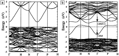 | ||
| Fig. 2 Band structures of (a) undoped and (b) Sn-doped In2O3. The Fermi level is set at E = 0 eV. The Brillouin zone centre is denoted by Γ, while H, N and P denote points at the Brillouin surface along high symmetry k-vectors in the reciprocal crystal lattice. The energy lines represent allowed electronic states at given k-points. Adapted with permission from Freeman et al.6 Copyright 2011 Cambridge University Press. | ||
The conductivity of a TCO is related to the number of charge carriers and their ability to move through its crystal lattice, i.e. their mobility. The mobility of electrons within an n-type TCO is inversely proportional to their effective mass. This is a quantity used to express the mass that the electrons appear to have when moving within a periodic solid, in which their mobility is affected by their response to local forces within the crystal, expressed relative to their true mass (me). The key factor here is the orbital overlap between the metal cation in a host lattice and the oxygen, since it has been shown computationally that the CB in TCOs has significant oxygen character. It has been observed that metal-oxide structures with predominant s-character of the cation at the CBM are correlated with the lowest electron effective masses, suggesting that the degree of cation-oxide orbital hybridisation is a key factor.7 It is therefore likely that for this reason, TCOs based on an e.g. TiO2 host structure (where the CBM has 3d-character) are generally observed to have higher effective masses than SnO2-hosted TCOs.8,9 The calculated CB with a lower effective mass is described as having higher dispersity, and appears visually as having higher curvature at the band edges.2,10 This relationship can be easily demonstrated; to a parabolic approximation, the energy E(k) of the CB at wavevector k close to the Brillouin zone centre can be expressed as:
 | (4) |
 | (5) |
| σ = neμ | (6) |
 | (7) |
| α = σn | (8) |
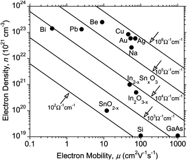 | ||
| Fig. 3 Boltzmann relation of electron density, mobility and hence, conductivity. The latter is displayed as straight-line contours. Adapted with permission from Edwards et al.10 Copyright 2004 Royal Society of Chemistry. | ||
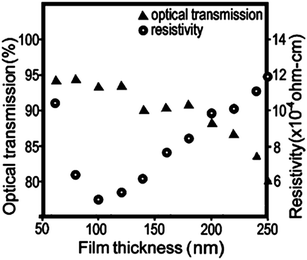 | ||
| Fig. 4 Effect on optical transmission and resistivity of increasing thickness of ITO film on PET substrate. Adapted with permission from Wong et al.12 Copyright 2004 Elsevier. | ||
The demand for TCOs has soared in recent years due to them being key components in liquid crystal displays, touch-screen technology and photovoltaic cells, usually as electrodes.13 Other applications amongst a growing number include antireflective coatings,14 waveguides in plasmonic devices,15 organic light-emitting devices12 and ‘lab-on-a-chip’ or bioanalytical devices.16 The current highest dollar-value market for TCOs is as transparent electrodes in flat-panel displays (FPDs), a market valued at US$ 97 Bn in 2014 and forecasted to reach US$ 135 Bn by 2020.17 Meanwhile, low-emissivity (‘low-e’) TCO window coatings account for the greatest amount of TCO deposited annually.18 Current European and US legislation requires that all new buildings must feature solar control window coatings, which has assisted such products as fluorine-doped tin oxide (FTO) coatings on glass to contribute to a multi-billion dollar market for low-e glass coatings.19 Ongoing social and technological development such as the increasing adoption of renewable energy sources and the continual growth of emerging economies therefore means that demand for TCOs is set to increase further and faster still.20
Later, in 1947, American inventor Harold McMaster patented a transparent conductive SnO2 coating which could be applied to glass via chemical vapour deposition (CVD) from stannous chloride, which became useful for planes when de-icing their windows at high altitude.23 Such TCO materials depend on oxygen vacancies and metal atom interstitials to lend conductivity, which are therefore not in practical use in modern TCOs due to the instability of such defects on longer timescales (i.e. gradual oxidation and interstitial migration). In 1954, Rupprecht discovered tin-doped indium oxide (ITO), a binary TCO material which to this day remains one of the most important and best-performing TCO materials on the market.24
In the decades that followed, countless transparent conducting oxide materials emerged from this fascinating field; in particular, while zinc oxide had long been known to be an intrinsic n-type semiconductor, its potential as a transparent conductor came to be recognised in research pioneered in the later 1970's to early 1980's by a fast-growing number of research groups, perhaps the most prolific of which being that of Minami et al.25 Work quickly moved on from intrinsically-doped ZnO, in which conductivity is owed to defects such as oxygen vacancies and hydrogen or zinc interstitials, to extrinsically-doped materials such as indium-doped zinc oxide (IZO).26 It was not long before the field exploded with many more n-type doped binary oxide systems for transparent conducting applications. Many of the most notable developments of this now expansive field shall be explored herein.
The relatively small concentration of dopant in the host material (typically 1–5 at%) is optimised by the trade-off between dopant carrier concentration versus increasing electron scattering effects at the dopant sites. This means that since free carrier densities in TCOs are low relative to metals, the mobility of the electrons within the TCO becomes the crucial factor in determining the conductivity of the material.29 It is also for this reason that TCO preparation methods which do not involve crystalline growth ultimately yield films with a high electrical resistance, i.e. that there is an abundance of physical boundaries which charge carriers must overcome and therefore their mobility is low. For example, indium-tin-oxide (ITO) thin films printed from a dispersion of 25 nm ITO nanoparticles, while achieving good optical transmittance at 84%, were only able to reach a minimum resistivity of 1.5 × 10⁻² Ω cm.28 Compare this with a typical polycrystalline ITO film grown by DC magnetron sputtering at 200 °C, which has a transmittance over 92% in the visible region and a much lower resistivity of 1.5 × 10⁻⁴ Ω cm.27 The reason for the discrepancy becomes more apparent in the scanning electron micrographs displayed in Fig. 5; it is evident that the polycrystalline film contains large (200–400 nm) well-oriented domains, while the inkjet-printed film of annealed nanoparticles contains a randomly-aligned physical boundary at the edge of each nanoparticle (i.e. every 25 nm). Therefore, due to the resistance faced by charge carriers at these physical boundaries, it would be expected that their mobility, and consequently the conductivity of the material, would be hampered in the annealed inkjet-printed film. As such, in choosing a synthetic procedure for a TCO product it is important to weigh the benefits of the technique against its cost, simplicity and safety, and the desired properties of the TCO material.
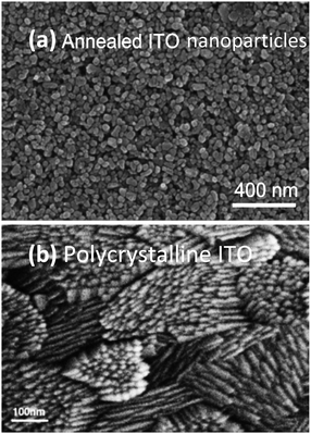 | ||
| Fig. 5 Scanning electron micrographs from (a) an ITO thin film inkjet-printed from 25 nm nanoparticles and annealed at 450 °C,28 and; (b) conventional DC magnetron sputtered polycrystalline ITO film deposited at 200 °C.27 Adapted with permission from Jeong et al. and Betz et al.27,28 Copyright (a) 2010 and (b) 2006 Elsevier. | ||
It is possible to tune the physical properties of the TCO in order to suit the application. For the PV heterojunction, to facilitate efficient charge transfer from the photo-absorbing layer to the TCO, there must also be optimal overlap of the energy levels of both layers, as determined by the TCO work function – this can be tuned by adjusting the relative concentration of components within a multi-component TCO.30 For instance, it was recently demonstrated by computation that the band gap of SnO2, which is sufficiently wide for visible transparency, can be controllably narrowed by alloying with isoelectronic PbO2, which has a narrow band gap but a large CBM to CBM + 1 gap and low electron effective mass. The properties of the alloying materials can combine to compliment one another, and in doing so, the CBM is lowered (i.e. the electron affinity is increased) to facilitate band alignment and Ohmic contact with other materials, while the Fermi level becomes positioned above the CBM to enable TCO functionality. The authors invite experimental verification.2
1.2 Indium-tin-oxide and the search for an alternative
Limited global supply has led to competition over the control of the resource and therefore limited availability of indium. The EU in particular is entirely dependent on imports for its indium supply, meaning that TCO manufacture within the EU, as well other indium-dependent low-carbon technologies such as nuclear control rod manufacture, suffers severely from the indium supply risk (see Fig. 6).20
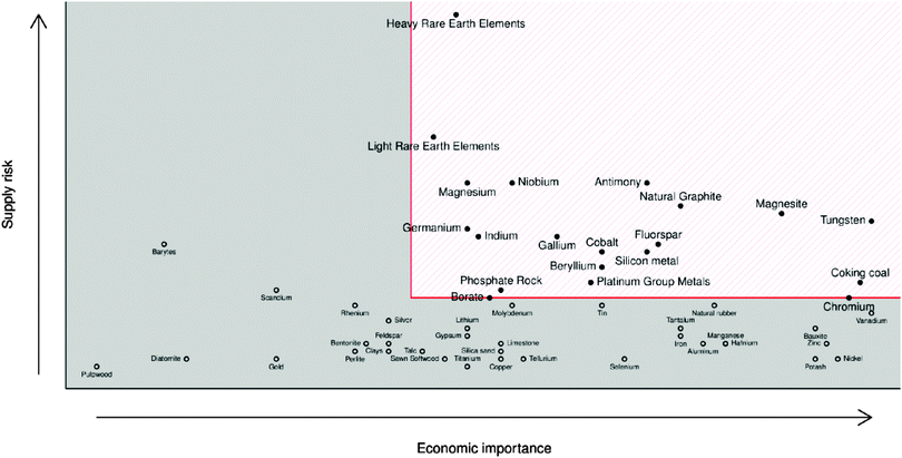 | ||
| Fig. 6 European Commission report for raw material criticality (2013 data, revised & published 2014).69 Adapted with permission from the European Commission. Copyright 2014 European Commission, DG Internal Market, Industry, Entrepreneurship and SMEs (DG GROW). | ||
Therefore, investigation into alternatives to the highly successful ITO as a TCO material has become necessary, in order to find cheaper, more capable, more earth-abundant materials. The search for a viable alternative seeks to optimise a number of figures of merit such as optical transmission, haze, resistivity, charge carrier concentration and mobility, etchability, ‘green’ processability and affordability. This wide range of desirable properties has led to some TCOs becoming preferable over others depending on the context of application, for example etchability in transparent circuitry or band alignment of a new TCO with other existing materials within an established device, with no single TCO formula therefore being universally ideal.7
2 n-Type doping of binary oxides
2.1 Background
As it stands, the industry standard TCOs used are largely limited to the post-transition metal oxides ZnO, In2O3 and SnO2, and subsequent mixtures of these such as tin- or zinc-doped indium oxide (ITO and IZO).18 The excellent metal-oxide orbital overlap in these structures gives rise to low electron effective masses (see Fig. 8) and therefore high electron mobilities. This, together with their deep CBMs (high dopability) and wide band gaps (see Fig. 7),2 is what makes these three important host structures for TCOs. Doped zinc oxide and tin oxide TCO materials have received particular attention in recent years on account of the indium supply risk,69 often with such dopants as to yield n-type TCOs (e.g. SnO2:F,36,37 SnO2:Sb,29,56–58 ZnO:F,40,41 ZnO:B,44–46 ZnO:Ga,48,49 ZnO:Al,47,70etc.). In particular, the heavy focus on n-type doping of SnO2 is probably owing in part to doubts within the community as to whether efficient p-type doped SnO2 can ever be realised.4 Much research has gone into investigating a number of dopant elements; in n-type TCOs, these are usually substitutional dopant atoms which are selected in such a way that excess electrons become available at the dopant site. A comparison of a number of experimentally-prepared n-type doped TCOs is given in Table 1, and can be referred to as a summary of the materials reviewed here. While the traditional ‘look-and-see’ approach of doping aliovalent atoms into crystal sites (e.g. Al3+ on a Zn2+ site or F− on an O2− site in ZnO) has been reasonably effective in the past for screening TCO materials, the seemingly endless range of possible permutations of metal-oxide host structures and dopants has more recently been narrowed significantly with the aid of high-throughput computational analysis.7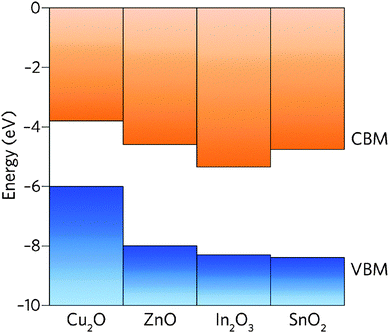 | ||
| Fig. 7 Calculated band gaps of common TCO host structures. The vacuum level is set at E = 0 eV. Adapted from Ganose.2 | ||
| Dopant class | Species | Type | Epitaxially-grown films | Polycrystalline films | ||||||||
|---|---|---|---|---|---|---|---|---|---|---|---|---|
| ρ/10−4 Ω cm | T/% | Preparation method | Ref. | ρ/10−4 Ω cm | T/% | Preparation method | Ref. | |||||
| Halides | SnO2:F (DC-MS) | n | 70.0 | 85 | dc-MS | 36 | (Mientus, 1998) | |||||
| SnO2:F (AACVD) | n | 2.2 | 80 | AACVD | 37 | (Bhachu, 2011) | ||||||
| SnO2:F (APCVD) | n | 5.2 | 80 | Commercial APCVD | 37 | (Bhachu, 2011) | ||||||
| TiO2:F | n | 16 | 95 | PLD | 38 | (Mohri, 2012) | 2.2 × 10³ | 40 | APCVD | 39 | (Kafizas, 2014) | |
| ZnO:F (PLD) | n | 4.8 | 90 | PLD | 40 | (Cao, 2011) | ||||||
| ZnO:F (APCVD) | n | 4.0 | 90 | APCVD | 41 | (Hu, 1991) | ||||||
| ZnO:Cl | n | 6.1 | 92 | PLD | 42 | (Lee, 2013) | 122.0 | 88 | ALD | 43 | (Choi, 2015) | |
| Gp XIII | ZnO:B (RF-MS) | n | 56.5 | 90 | rf-MS | 44 | (Wong, 2015) | |||||
| ZnO:B (Spr. Pyr.) | n | 45.0 | 95 | Spray pyrolysis | 45 | (Pawar, 2009) | ||||||
| ZnO:B (AACVD) | n | 15.0 | 90 | AACVD | 46 | (Shirahata, 2015) | ||||||
| ZnO:Al | n | 0.85 | 88 | PLD | 47 | (Agura, 2003) | 2.0 | 80 | rf-MS | (Minami, 1984) | ||
| ZnO:Ga | n | 0.51 | 85 | Buffer-assisted PLD | 48 | (Ajimsha, 2015) | 2.7 | 85 | rf-MS | 49 | (Assunção, 2003) | |
| ITO | n | 0.77 | 85 | PLD | 50 | (Ohta, 2000) | 1.5 | 92 | dc-MS | 27 | (Betz, 2006) | |
| Gp III | ZnO:Sc | n | 1.91 | 92 | Sol–gel | 51 | (Sharma, 2010) | 3.1 | 85 | dc-MS | 52 | (Minami, 2000) |
| ZnO:Y | n | 7.9 | 85 | dc-MS | 52 | (Minami, 2000) | ||||||
| Gp XV | SnO2:N | p | 9.1 | 80 | rf-MS | 33 | (Fang, 2015) | |||||
| SnO2:P | n | 7.0 | 83 | APCVD | 53 | (Upadhyay, 1989) | ||||||
| TiO2:P | n | 1.7 × 10⁴ | 70 | APCVD | 54 | (Sotelo-Vazquez, 2015) | ||||||
| SnO2:As | n | 460.0 | 80 | Vacuum thermal evaporation | 55 | (Dakhel, 2012) | ||||||
| SnO2:Sb (RF-MS) | n | 6.7 | — | Plasma-assisted MBE | 56 | (White, 2009) | 20.0 | 85 | rf-MS | 57 | (Ma, 2003) | |
| SnO2:Sb (APCVD) | n | 15.0 | 80 | APCVD | 58 | (Kane, 1976) | ||||||
| SnO2:Sb (Spr. Pyr.) | n | 9.0 | 80 | Spray pyrolysis | 29 | (Shanthi, 1999) | ||||||
| ZnO:Sb (p-type) | p (Sb III) | 2000 | — | MBE | 59 | (Xiu, 2005) | 1.9 × 10⁷ | — | APCVD | 60 | (Liang, 2015) | |
| ZnO:Sb (n-type) | n (Sb V) | 4.2 × 10³ | — | APCVD | 60 | (Liang, 2015) | ||||||
| Gp V | TiO2:V (p-type) | p | 8.0 × 10⁸ | 81 | Reactive-MS | 61 | (Sieradzka, 2009) | |||||
| TiO2:V (n-type) | n | 6.0 × 10⁶ | 81 | Reactive-MS | 61 | (Sieradzka, 2009) | ||||||
| TiO2:Nb | n | 2.3 | 95 | PLD | 62 | (Furubayashi, 2005) | 4.6 | 70 | PLD | 63 | (Hitosugi, 2007) | |
| TiO2:Ta | n | 2.5 | 95 | PLD | 64 | (Hitosugi, 2005) | 8.7 | 80 | PLD | 65 | (Wu, 2011) | |
| Other | Graphene | n | 18.2 | 65 | Mechanical exfoliation and reduction | 66 | (Wang, 2008) | |||||
| Carbon nanonets | p | 1.5 | 70 | Vacuum membrane deposition | 67 | (Wu, 2004) | ||||||
Computational simulations of hypothetical TCO materials have enabled screening of a wide range of possible materials and their properties, enabling us, with more power than ever before, to narrow the search of the many possible combinations of metal-oxide host and p-type or n-type dopants and their concentrations. It is possible to model the band structures, electron effective masses and mobilities in this way. Perhaps unfortunately, in one particular landmark high-throughput computational study, one of the most effective TCO materials amongst thousands of alternatives was found to remain the tin-doped indium oxide (ITO), the present industry standard TCO, though there are of course errors associated with computational modelling techniques; in particular, that Generalised Gradient Approximation (GGA) functionals in density functional theory (DFT) are known to strongly underestimate band gaps, and electron effective masses are generally underestimated within DFT itself. Still, the error appears to be systematic, meaning this remains a useful tool for comparative screening of materials at the early stages.7
2.2 Group IIIA- and IIIB-doped ZnO
GZOs have attracted particular attention due to the close matching of Ga3+ and Zn2+ ionic radii, while Ga also effects a lower electron effective mass in the TCO (see Fig. 8); both of these factors are therefore more likely to result in higher electron mobilities in n-type GZO TCOs. However, while GZO and AZO films are competitive with each other in terms of TCO properties, the affordability and natural abundance of Al makes this a particularly attractive dopant material in TCO production, whereas in 2014 the supply risk of Ga was closely comparable with that of In (see Fig. 6).69
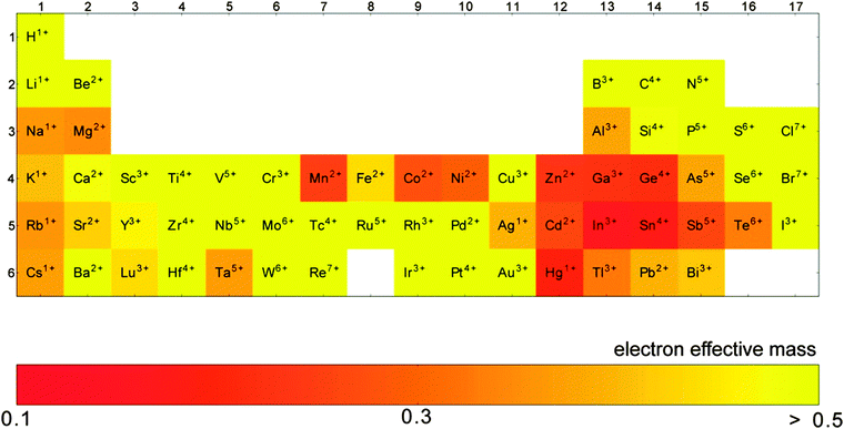 | ||
| Fig. 8 Computation of the elements which exhibit the lowest electron effective masses in their respective binary oxides. Adapted with permission from Hautier et al.7 Copyright 2014 American Chemical Society. | ||
AZOs have been synthesised by a number of means including atmospheric-pressure (thermal) chemical vapour deposition,72 RF and DC magnetron sputtering,78,79 atomic layer deposition,80 pulsed laser deposition,81 sol–gel82 and spray pyrolysis techniques.71 AZOs, like any trivalent-doped n-type ZnO TCO, work by substituting an Al3+ ion into a Zn2+ site, leaving an excess electron at the substituted site and therefore leading to n-type conductivity. In principle, the conductivity of the doped films can therefore be improved by increasing the dopant concentration (and therefore the free carrier concentration). However, the trouble with minimising resistivity by ramping up the carrier concentration is that having a carrier concentration anywhere over ca. 2 × 1021 cm−3 causes a shift of the plasma edge in the absorption spectrum from the infrared into the visible region, resulting in coloured films in extreme cases,31 while also reducing the free carrier relaxation time due to an increase in the concentration of scattering sites. The negative impact on resistivity and optical transmission of increasing the dopant concentration beyond its optimum is similar to that of increasing film thickness (Fig. 4), since an increased number of scattering sites and charge carriers leads to decreased mobility and a more pronounced free carrier absorption (FCA) effect.
Perhaps the upper limit of a TCO's potential optoelectronic properties can be represented by the monocrystalline film, in which the major obstacle to carrier mobility is simply the dopant concentration rather than the grain boundaries, the latter being the case with the more practical polycrystalline films. A comparison of the conductivities of epitaxially-grown monocrystalline TCOs is given in Fig. 9, while the polycrystalline films are compared in Fig. 10. Monocrystalline AZO grown epitaxially using pulsed laser deposition (PLD) exhibits a resistivity of ρ = 8.5 × 10⁻⁵ Ω cm;47 polycrystalline AZO has been deposited by RF magnetron sputtering (rf-MS) with around ρ = 2 × 10⁻⁴ Ω cm.70 Commercial polycrystalline ITO grown by DC magnetron sputtering (dc-MS) typically exhibits ρ = 1.5 × 10⁻⁴ Ω cm,27 so from this point of view, AZO appears to be a very competitive alternative. However, an issue encountered in the past with magnetron sputtering deposition of electrically conductive doped ZnO films has been the relative sensitivity of Zn to the strength of the oxidising environment in which the films are deposited, on account of the increased chemical activity of Zn in such environments as compared with deposition of In or Sn oxides. The result is an uneven distribution of electrical conductivity in large-area AZO films, which places limitations on their utility.76
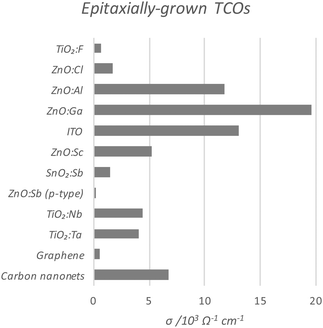 | ||
| Fig. 9 Comparison of conductivities of epitaxially-grown monocrystalline transparent conducting oxides, as compared with current conventional carbon-based TCMs. The full data set with author references is given in Table 1. | ||
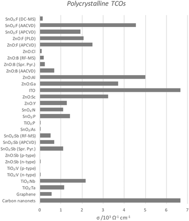 | ||
| Fig. 10 Comparison of conductivities of polycrystalline TCOs deposited by various means, as also compared with current carbon TCMs. The full data set with author references is given in Table 1. Abbreviations: aerosol-assisted or atmospheric pressure chemical vapour deposition (AA- or AP-CVD), radiofrequency or direct current magnetron sputtering (RF- or DC-MS), spray pyrolysis (Spr. Pyr.). | ||
It is important to note that, while epitaxial methods for growing films on crystalline substrates are useful for demonstrating the upper limits of the properties of a particular TCO material, most industrial deposition techniques are more likely to yield polycrystalline films, in particular atmospheric-pressure (thermal) chemical vapour deposition (APCVD) and dc-MS. By its nature, PLD is generally not easily scalable for industrial large-area film deposition where hundreds of square metres rather than a few square centimetres need to be covered at an appreciable rate of film growth.83 Therefore, while epitaxial PLD films may be representative of the ideal case for a film, providing an upper limit to the properties achievable for a given TCO formula, it is perhaps more useful for us to compare the properties of TCOs deposited by scalable methods such as APCVD or magnetron sputtering.
| Class | Element | O.S. | C.N. | Ionic radius/Å |
|---|---|---|---|---|
| Host | O | −2 | 2/3/4 | 1.4 |
| Sn | +4 | 6 | 0.69 | |
| Zn | +2 | 4 | 0.60 | |
| Ti | +4 | 6 | 0.61 | |
| Halides | F | −1 | 2/3/4 | 1.3 |
| Cl | −1 | 4 | 1.81 | |
| Gp XIII | B | +3 | 4 | 0.12 |
| Al | +3 | 4 | 0.39 | |
| Ga | +3 | 4 | 0.47 | |
| In | +3 | 6 | 0.79 | |
| Gp III | Sc | +3 | 6 | 0.73 |
| Y | +3 | 6 | 0.89 | |
| Gp XV | N | −3 | 4 | 1.32 |
| P | +5 | 4 | 0.17 | |
| As | +5 | 6 | 0.50 | |
| Sb | +3 | 4 | 0.77 | |
| Sb | +5 | 6 | 0.61 | |
| Gp V | V | +3 | 6 | 0.64 |
| V | +5 | 6 | 0.54 | |
| Nb | +5 | 6 | 0.64 | |
| Ta | +5 | 6 | 0.64 | |
2.3 Group VA- and VB-doped TiO2 and SnO2
Recent work has found that substitution of Ti atoms in the anatase TiO2 tetragonal cell with group VB metal atoms such as Nb or Ta transforms the intrinsically semiconducting TiO2 into an effective TCO with previously recorded resistivities reaching as low as ρ = 2–3 × 10⁻⁴ Ω cm for both the Ta- and Nb-doped anatase films epitaxially grown by PLD,62 while the best apparent polycrystalline films synthesised have ρ = 4.6 × 10⁻⁴ Ω cm and 8.7 × 10⁻⁴ Ω cm for TiO2:Nb and TiO2:Ta respectively.63,65 Computational studies have disagreed on which of Ta or Nb shows more promise as a dopant in anatase TiO2, since while the two have similar ionic radii (see Table 2), the studies differ on the discussion of Ta doping. On the one hand, Ta is reported to effect a greater local distortion of the crystal lattice than Nb, potentially impeding both charge carrier mobility and crystal growth; on the other hand, Ta is also reported to have both higher solubility in anatase than Nb and a lower effective mass band structure (see Fig. 8), which leads to increased mobilities.9,86 In any case, in spite of TiO2:(Nb,Ta) having very similar properties in the epitaxial films, experimental results consistently indicate that the Nb-doped TiO2 are the better-performing of the polycrystalline films; the fact that TiO2:Nb accounts for a significantly greater portion of recent research than its Ta-doped counterpart is reflective of this.84 However, while Nb is considered by the European Commission to have a critical supply risk (greater even than In), Ta was removed in 2013 from the category due to a reduction in the supply risk, on account of increased global supply from Australia and, more recently, Brazil.69
The earliest examples of studies detailing the syntheses of TiO2:Ta and TiO2:Nb are a pair of 2005 papers in which the films were grown epitaxially on SrTiO3 (001) and LaAlO3 (001) crystalline substrates by PLD.62,64 These films formed a new class of TCO whose conductivity was dependent on d-electrons, in contrast to typical TCO materials in which s- or p-electrons are more commonly responsible for conductivity,64 due to TiO2 being the only widely investigated transition-metal-oxide (i.e. d-block) host material for TCOs. It is thought that the spins associated with d-electrons may lead to new applications for this class of TCOs in spintronic devices.87
One issue with Ti1−xNbxO2 is the strong optical absorption in the red proportional to dopant concentrations over approximately x = 0.03. The result is strongly blue-coloured films.62,88,89 The origin of this effect is the narrow band gap between the occupied CBM and CBM + 1 in the doped films, which is evident in Fig. 11, giving rise to a pronounced free carrier absorption (FCA) effect.89 Unfortunately, in order that polycrystalline Ti1−xNbxO2 should have competitive resistivities (i.e., ρ < 10−3 Ω cm), it is necessary to have x ≥ 0.06, which gives rise to a significant blue colouration effect.63,88 This is a desirable property in certain applications such as some window coatings, however it does preclude the use of TiO2:Nb TCOs in applications where transmission of a full visible spectrum is required e.g. mainstream flat panel displays (FPDs). In general, TiO2-based TCOs tend to possess a high refractive index, which has also been linked to colouration due to intrinsic interference effects.87 On the other hand, a reduced optical band gap appears to be preferable in photocatalytic applications, in which the absorption of light both in the UV and in the visible promotes catalytic efficiency. Certain circumstances may therefore call for a film which is at once transparent, conducting and photocatalytically active. Indeed, much research presently investigates the doping of TiO2 in order to increase photocatalytic activity by absorption of visible light.90,91
 | ||
| Fig. 11 Calculated electronic band structures of (a) TiO2 and (b) TiO2:Nb. The Brillouin zone centre is denoted by Γ, while X, R, Z, M and A denote points at the Brillouin surface along high symmetry k-vectors in the reciprocal crystal lattice. The lines represent allowed electronic energy states at given k-points. Adapted with permission from Hitosugi et al.89 Copyright 2008 The Japan Society of Applied Physics. | ||
In the case of Ta-doped SnO2, while the low electron effective masses in the SnO2 host are attractive (see Fig. 8), the ability to tailor conductivity of SnO2:Ta by varying dopant levels is restricted somewhat by the thermodynamic competition of the pseudo-binary phase SnO2:TaO2 with the ternary phase SnTa2O6, as well as the trapping of electrons at Ta5+ sites due to local Jahn–Teller distortion, also associated with high dopant levels. A combination of these two key factors places an upper limit on the conductivity of SnO2:Ta, with a maximum conductivity predicted using first-principles computation at a dopant concentration of approximately 1 at% Ta. The same is also true of Nb-doped SnO2, where the optimal doping level lies around 2 at% Nb.92
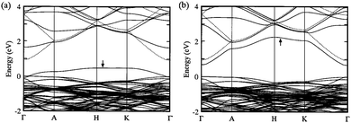 | ||
| Fig. 12 Calculated band structure for ZnO supercells with (a) oxygen vacancy and (b) zinc interstitial. Note the direct competition of (a) p-type and (b) n-type conductivity between the two defect species. The valence band maximum is defined at zero energy. The highest occupied state is indicated by an arrow in each. Adapted with permission from Oba et al.99 Copyright 2001 AIP Publishing LLC. | ||
Perhaps more electrically competitive is the arsenic-doped SnO2:As, which was deposited in the late 1980s via APCVD to yield films which claimed ρ = 1.5 × 10⁻⁴ Ω cm,98 although efforts since then have been unable to achieve such low resistivity.55 Around the same time, that group found that SnO2:P deposited in a similar manner was capable of ρ = 7.0 × 10⁻⁴ Ω cm.53
A recent computational study has found that of the group VA dopants (P, As, Sb, Bi) in SnO2, only P and Sb are effective n-type donors due to the change in oxidation state from V to III of As and Bi substituted sites as the Fermi level approaches the CBM.8,100 However, another experimental study has shown that P can also exhibit multiple oxidation states (namely P5+ and P3−) in a TiO2:P TCO depending on the conditions of the deposition, and that P3− incorporation is overall detrimental to its electronic and photocatalytic properties.54
2.4 Halide dopants
Unlike cation dopants which substitute metal ion sites, halide dopants substitute at the oxygen sites and are therefore more widely dopable into metal-oxide TCO hosts to produce n-type SnO2:F, ZnO:F and TiO2:F.37,38,41 The most widespread TCO material containing a halide dopant is fluorine-doped tin oxide (FTO), which is widely produced industrially as an important low-emissivity window coating due to its reflectivity in the infrared region (see Fig. 13). Of the halides, F− is the most effective dopant for TCOs due to its excellent matching of the O2− ionic radius (see Table 2). For this reason, larger halide dopants such as Cl− are less stable substitutional defects in a metal oxide crystal on account of the exertion of strain on the local environment – such strains restrict charge carrier mobility and phonon propagation, as well as encouraging unstable interstitial Cl− and thermal ion migration.43 FTO is therefore the favoured halide-doped TCO, with excellent thermal and chemical stability, transmissivity in the visible exceeding 85%, excellent IR reflectivity as well as being inexpensive and chemically robust.36,37,104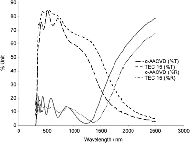 | ||
| Fig. 13 Optical transmittance (%T) and reflectance (%R) spectra of SnO2:F lab-grown by combinatorial aerosol-assisted chemical vapour deposition (c-AACVD) as compared with an industrial SnO2:F product (TEC 15, Pilkington NSG). Adapted with permission from Bhachu et al.37 Copyright 2011 Wiley. | ||
The most electrically conducting FTO thin film deposited by magnetron sputtering methods has achieved 7.0 × 10⁻³ Ω cm,36 though in more recent years, aerosol-assisted chemical vapour deposition methods have reached resistivities an order of magnitude lower, down to 2.2 × 10⁻⁴ Ω cm.37 Currently one of the best-performing mass-produced FTO thin films on the market, as delivered by on-line atmospheric-pressure CVD (APCVD), is TEC-8 (Pilkington NSG) with ρ = 5.2 × 10⁻⁴ Ω cm.37 The generation of aerosols in AACVD as a means of precursor transport has shown much promise in recent years as an alternative to ‘traditional’ thermal- or AP-CVD, which requires that the precursor has sufficient vapour pressure in order to be transported in the vapour phase.105,106 By instead generating an aerosol from the precursor, the vapour pressure requirement is sidestepped as well as producing some interesting morphologies, and therefore properties, in the deposited films.37 FTO studies in recent years have therefore investigated alternatives to the commercial APCVD process such as AACVD37 and also spray pyrolysis,104 both of which have produced highly competitive FTO films.
More recently, F-doped anatase TiO2 has also attracted some attention, whose mediocre electronic properties (ρ = 1.6 × 10⁻³ Ω cm in the epitaxial film,38ρ = 2.2 × 10⁻¹ Ω cm in the polycrystalline film39) are compensated by its exhibition of promising photocatalytic behaviour.90,91 The resistivity of these films is several times higher than Nb- or Ta-doped anatase, and has been attributed to a combination of the low doping efficiency of F in anatase (20–30% for F compared with 70–100% for Nb and Ta in anatase) and the high effective mass of free electrons in an F-doped crystal. It has been postulated that the fluoride sites act to trap the electrons, limiting their mobility.38 On the other hand, the F dopant also serves to narrow the optical band gap by stabilisation of Ti3+ and VO sites, producing a donor level at the CBM and limiting electron–hole recombination. This facilitates a broader optical absorption profile, so that the films are able to utilise the visible portion of the spectrum for indoor photocatalytic applications. As such, the TiO2:F films have been found to perform significantly better than pure anatase in a photocatalytic test (photoinduced degradation of methylene blue dye).90
Also interesting are F-doped ZnO films (FZO), which were successfully deposited by APCVD in the early 1990s with excellent optoelectronic properties (ρ = 4.0 × 10⁻⁴ Ω cm, mobilities up to μ = 40 cm2 V−1 s−1, 90% visible transmittance, 85% IR reflectance and up to 90% quantum efficiency in a-Si solar cells).41 The lack of interest into FZOs since then could be due to the far more widespread research into AZOs, which are more competitive as earth-abundant n-type ZnO-based TCOs. On the other hand, recent authors have noted that the shortage in FZO study is in part due to difficulties with finding suitable precursors for FZO deposition.107
2.5 Carbon competitors
Transparent electrode materials other than TCOs have also arisen in recent years; for instance, atom-thick graphene layers have been used for their similarly excellent optical transmission properties (∼2.3% visible light absorbed per graphene layer), their exceedingly high electron mobilities coupled with low carrier concentration (∼103–104 cm2 V−1 s−1 and ∼1013 cm−2 respectively)108 and their mechanical flexibility. Graphene electrodes are operable in a solar cell device under bending at 138°, compared with maximum operable bending angle of 60° in the more brittle indium tin oxide (ITO) TCO cell.35 However, for the sheet resistance of graphene to be competitive with ITO, at least four monolayers of graphene are required, which results in a significant loss of optical transmission in the graphene (typically about 10% less transmittance than ITO).109 Furthermore, optical transmission in the graphene drops off dramatically at light incidence angles greater than about 30°, which is a concern not only for information displays but also for the efficiency of graphene-based organic photovoltaic devices (OPVs), where ITO remains the most effective electrode material, which suffers virtually no drop-off in transmission from an increased incidence angle.109 A further issue arises in graphene-based OPVs on account of its hydrophobicity; this makes aqueous solution processing problematic, particularly in binding the graphene to the hole-transporting layer (HTL) material poly(3,4-ethylenedioxythiophene):poly(styrene sulfonate) (PEDOT:PSS) which consequently impacts the power conversion efficiency (PCE) of the OPV.110 As such, graphene OPVs can only achieve a maximum PCE of approximately 60% that of ITO-based OPVs. Nevertheless, some work has gone towards resolving this issue by doping the graphene electrode111 as well as trialling alternative HTL materials.112 Carbon nanonet thin films, on the other hand, comprise stacks of randomly oriented single-walled carbon nanotubes (SWCNTs) to a thickness of approximately 50 nm, which have demonstrated, like graphene TCMs, excellent transmission in the infra-red, while ITO and other TCOs are often reflective in this region; on the other hand, this IR transmissivity comes at the expense of the visible region of the spectrum, in which the carbon-based TCMs have only ∼70% transmittance, compared with 80–95% visible transmittance in TCOs. Therefore, as it stands, it appears that the carbon-based films might be useful in more niche situations than the TCOs, such as flexible electronics or military applications.673 Transparent electrodes in application
Myriad modern devices adopt transparent conducting oxide thin films, in virtually every and any optoelectronic context from solar power generation to information displays. In many of these cases, ITO seems to be the most prevalent TCO material adopted, which is problematic for the reasons discussed thus far, with indium's high supply risk at the fore. It has become generally desirable to move away from ITO and begin adopting alternative TCO materials. However, new demand for TCO development is arising in the field of transparent electronics, in which alternatives to ITO are not only desirable from a cost perspective, but also preferable from the technical perspective.3.1 Transparent information displays
Development in the fields of both transparent conducting thin films and active matrix organic light emitting diode (AMOLED) displays has resulted in their joining to form a new and exciting kind of product: transparent AMOLED displays. While transparent OLED (TOLED) displays have been in development since the mid-1990s,113 early devices were comprised of a high work function TCO anode (usually ITO) with a low work function metal cathode (e.g. Ca, Au or Ag–Mg) sandwiching an organic semiconductor layer with hole (HTL) and electron (ETL) transport layers in the intermediate (see Fig. 14). However, the adoption of even a thin metallic cathode layer sets an upper limit to the optical transparency of only around 50%.114 While prototype transparent televisions have now been developed and showcased by tech giants such as Samsung, these seem to adopt twin ITO electrodes,115 wherein the challenge remains to find a cathode material with comparable optical transmittance and electrical resistivity to ITO but a lower work function for more efficient electron injection. Work is ongoing to meet this challenge; for instance, it has been observed both experimentally116 and computationally117 that extrinsic doping of zinc oxide with e.g. Al or Ga, such that the surface charge carrier density is increased, will effectively lower its work function at the interface. Likewise, recent work has also sought to raise the work function of the ITO anode, in order to improve band alignment with the HTL layer and thus overall improve device efficiency.118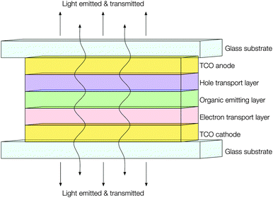 | ||
| Fig. 14 Schematic illustrating the construction of a transparent AMOLED device adopting TCOs for both electrodes. | ||
Aside from this, the usual means of depositing an ITO cathode industrially via sputtering is damaging to the underlying organic layers of the OLED device;119 this issue has thus far been addressed by deposition of additional protective buffer layers via e.g. thermal evaporation prior to the sputtering stage,115 however this perhaps adds needless complication and expense when an alternative deposition means (e.g. chemical vapour deposition) for the TCO cathode can be sought. Indeed, it has been seen that with many TCO films including ZnO:B, SnO2:Sb and SnO2:F, the chemical vapour deposition route will actually often produce films with superior optoelectronic properties to those obtained via sputtering.36,37,44,46,57,58
Much has been learned in recent years through computational modelling and experimental verification regarding the tuneability of the work function of doped transparent conducting oxide materials,2,117,118 and it is anticipated that the continuing relationship between computational and experimental methods will deliver tangible development to this rapidly evolving field.
3.2 Transparent photovoltaic cells
The design of a conventional photovoltaic (PV) cell bears much resemblance to that of an AMOLED device; that is, that a TCO anode is deposited upon a glass substrate, followed by an HTL (e.g. poly(3,4-ethylenedioxythiophene) polystyrene sulfonate, ‘PEDOT:PSS’). Upon the HTL is deposited the photoactive layer, which is at last bound directly to a reflective metallic cathode; where a low-work function metallic cathode is used, there is sometimes no need for an intermediary ETL.120 Again, ITO is the most commonly adopted TCO anode material in a PV cell, and therefore PV design is yet another technology which stands to benefit from shifting away from ITO towards more affordable and earth-abundant TCO electrodes. But as AMOLED displays now strive for transparency, so too does the conventional PV cell.By combining solar energy generation with, for example, architectural glass applications, there suddenly arises the exciting new prospect of self-sustaining cities designed and built to meet their own energy demands, or mobile phones which charge themselves in open daylight. True, efficiency in a transparent PV device as compared with an opaque one will inevitably suffer due to the sacrifice of the visible portion of the spectrum (and therefore the increased dependence on incident UV intensity); however, should these become cheap enough to manufacture, they should be able in principle to become far more pervasive than their opaque analogues due to their ability to be installed almost anywhere and on any device.
Similar technical obstacles face transparent PVs as do TOLEDs – that is, that the metallic cathode ought to be replaced with a highly optically transmissive material with a sufficiently low work function and resistivity so as to facilitate electron injection and distribution (see Fig. 15). Currently transparent PVs appear to be adopting thin metal films for this purpose, which limits their transparency and therefore their utility.121 This is just one issue amongst many more which may be tackled by the continued development of n-type doped TCO electrodes, which serves to illustrate the unique utility and value of these ubiquitous and powerful materials.
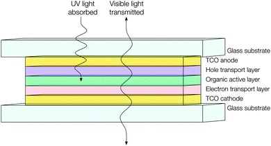 | ||
| Fig. 15 Schematic of a hypothetical transparent organic photovoltaic device adopting TCO materials for both electrodes. | ||
4 Summary
In this state-of-the-art review, both prominent and lesser-known doped binary oxide systems have been reviewed for their utility as transparent conducting electrodes and other important roles. Such materials are of great importance to modern technology, and play a particularly significant role in the global economy. As such, these materials have been considered from both a functional and economic standpoint, given that both factors have equal weight as stimuli for further research. Given the multi-functional roles of these materials, there are a number of factors to be optimised depending on the application; for this reason, there is no ‘catch-all’ material, and the individual benefits and shortfalls of each material have been discussed, while a more general visual review of about thirty materials compares their resistivities and visible transmittances. The mechanism for the functionality of these materials has been discussed, with regard to the chemical and physical factors which combine to produce the observed phenomena, with particular focus on the now-indispensable dialogue between experimental and computational study. A number of systems have been identified from both computational and experimental studies with potential for further investigation, as well as placing a brief spotlight on some ongoing technological challenges which may yet be solved by further development of transparent conducting oxide thin films.Acknowledgements
Mr Alex Ganose is thanked for his assistance with producing Fig. 1. NSG Pilkington Glass and the EPSRC are thanked for their funding through the Molecular Modelling and Material Science (M3S) Doctoral Training Centre at UCL (EP/G036675) and for grants EP/L017709, EP/K001515 and EP/N01572X.Notes and references
- K. Hayashi, S. Matsuishi, T. Kamiya, M. Hirano and H. Hosono, Nature, 2002, 419, 462–465 CrossRef CAS PubMed
.
- A. M. Ganose and D. O. Scanlon, J. Mater. Chem. C, 2016, 4, 1467–1475 RSC
.
- E. Burstein, Phys. Rev., 1954, 93, 632–633 CrossRef CAS
.
- D. O. Scanlon and G. W. Watson, J. Mater. Chem., 2012, 22, 25236 RSC
.
- A. Walsh, J. Buckeridge, C. R. A. Catlow, A. J. Jackson, T. W. Keal, M. Miskufova, P. Sherwood, S. A. Shevlin, M. B. Watkins, S. M. Woodley and A. A. Sokol, Chem. Mater., 2013, 25, 2924–2926 CrossRef CAS
.
- A. J. Freeman, K. R. Poeppelmeier, T. O. Mason, R. P. H. Chang and T. J. Marks, MRS Bull., 2000, 25, 45–51 CrossRef CAS
.
- G. Hautier, A. Miglio, D. Waroquiers, G.-M. Rignanese and X. Gonze, Chem. Mater., 2014, 26, 5447–5458 CrossRef CAS
.
- D. Cheng, M. Zhang, J. Chen, C. Yang, X. Zeng and D. Cao, J. Phys. Chem. C, 2014, 118, 2037–2043 CAS
.
- H. Anh Huy, B. Aradi, T. Frauenheim and P. Deák, J. Appl. Phys., 2012, 112, 016103 CrossRef
.
- P. P. Edwards, A. Porch, M. O. Jones, D. V Morgan and R. M. Perks, Dalton Trans., 2004, 2995 RSC
.
- H. Peelaers, E. Kioupakis and C. G. Van de Walle, Appl. Phys. Lett., 2012, 100, 011914 CrossRef
.
- F. L. Wong, M. K. Fung, S. W. Tong, C. S. Lee and S. T. Lee, Thin Solid Films, 2004, 466, 225–230 CrossRef CAS
.
- D. S. Ginley and C. Bright, MRS Bull., 2000, 25, 15–18 CrossRef CAS
.
- J. Cai and L. Qi, Mater. Horiz., 2015, 2, 37–53 RSC
.
- Y. Lin, X. Zhang, S. Bai and A. Hu, J. Mater. Chem. C, 2015, 3, 6046–6052 RSC
.
- R. B. Fair, Microfluid. Nanofluid., 2007, 3, 245–281 CrossRef CAS
.
- Future Market Insights, Flat Panel Display Market: Global Industry Analysis and Opportunity Assessment 2014–2020, 2015.
-
C. I. Bright, in 50 Years of Vacuum Coating Technology and the Growth of the Society of Vacuum Coaters, ed. D. M. Mattox and V. H. Mattox, Society of Vacuum Coaters, 2007, p. 38 Search PubMed
.
-
T. M. Letcher and J. L. Scott, Materials for a Sustainable Future, Royal Society of Chemistry, 2012 Search PubMed
.
-
R. L. Moss, E. Tzimas, H. Kara, P. Willis and J. Kooroshy, Critical Metals in Strategic Energy Technologies, 2011 Search PubMed
.
- M. Grundmann, Phys. Status Solidi, 2015, 212, 1409–1426 CrossRef CAS
.
- A. Wang, J. R. Babcock, N. L. Edleman, A. W. Metz, M. A. Lane, R. Asahi, V. P. Dravid, C. R. Kannewurf, A. J. Freeman and T. J. Marks, Proc. Natl. Acad. Sci. U. S. A., 2001, 98, 7113–7116 CrossRef CAS PubMed
.
-
H. Mcmaster, US Pat., 2429420, 1947 Search PubMed
.
- G. Rupprecht, Z. Phys., 1954, 139, 504–517 CrossRef CAS
.
- T. Minami, Appl. Phys. Lett., 1982, 41, 958 CrossRef CAS
.
- S. Major, A. Banerjee and K. L. Chopra, Thin Solid Films, 1983, 108, 333–340 CrossRef CAS
.
- U. Betz, M. Kharrazi Olsson, J. Marthy, M. F. Escolá and F. Atamny, Surf. Coat. Technol., 2006, 200, 5751–5759 CrossRef CAS
.
- J.-A. Jeong, J. Lee, H. Kim, H.-K. Kim and S.-I. Na, Sol. Energy Mater. Sol. Cells, 2010, 94, 1840–1844 CrossRef CAS
.
- S. Shanthi, C. Subramanian and P. Ramasamy, J. Cryst. Growth, 1999, 197, 858–864 CrossRef CAS
.
-
D. S. Ginley, H. Hosono and D. C. Paine, Handbook of Transparent Conductors, 2010 Search PubMed
.
- C. Guillén and J. Herrero, Thin Solid Films, 2011, 520, 1–17 CrossRef
.
- H. Kim, J. S. Horwitz, G. P. Kushto, Z. H. Kafafi and D. B. Chrisey, Appl. Phys. Lett., 2001, 79, 284 CrossRef CAS
.
- F. Fang, Y. Zhang, X. Wu, Q. Shao and Z. Xie, Mater. Res. Bull., 2015, 68, 240–244 CrossRef CAS
.
- Y. F. Lan, W. C. Peng, Y. H. Lo and J. L. He, Org. Electron., 2010, 11, 670–676 CrossRef CAS
.
- L. Gomez De Arco, Y. Zhang, C. W. Schlenker, K. Ryu, M. E. Thompson and C. Zhou, ACS Nano, 2010, 4, 2865–2873 CrossRef CAS PubMed
.
- R. Mientus and K. Ellmer, Surf. Coat. Technol., 1998, 98, 1267–1271 CrossRef CAS
.
- D. S. Bhachu, M. R. Waugh, K. Zeissler, W. R. Branford and I. P. Parkin, Chem. – Eur. J., 2011, 17, 11613–11621 CrossRef CAS PubMed
.
- S. Mohri, Y. Hirose, S. Nakao, N. Yamada, T. Shimada and T. Hasegawa, J. Appl. Phys., 2012, 111, 093528 CrossRef
.
- A. Kafizas, N. Noor, P. Carmichael, D. O. Scanlon, C. J. Carmalt and I. P. Parkin, Adv. Funct. Mater., 2014, 24, 1758–1771 CrossRef CAS
.
- L. Cao, L. Zhu, J. Jiang, R. Zhao, Z. Ye and B. Zhao, Sol. Energy Mater. Sol. Cells, 2011, 95, 894–898 CrossRef CAS
.
- J. Hu and R. G. Gordon, Sol. Cells, 1991, 30, 437–450 CrossRef CAS
.
- J. Lee, N. G. Subramaniam, J. Lee, J. Lee and T. Kang, Phys. Status Solidi, 2013, 210, 2638–2643 CrossRef CAS
.
- Y.-J. Choi, K.-M. Kang, H.-S. Lee and H.-H. Park, J. Mater. Chem. C, 2015, 3, 8336–8343 RSC
.
- L.-H. Wong and Y.-S. Lai, Thin Solid Films, 2015, 583, 205–211 CrossRef CAS
.
- B. N. Pawar, G. Cai, D. Ham, R. S. Mane, T. Ganesh, A. Ghule, R. Sharma, K. D. Jadhava and S.-H. Han, Sol. Energy Mater. Sol. Cells, 2009, 93, 524–527 CrossRef CAS
.
- T. Shirahata, T. Kawaharamura, S. Fujita and H. Orita, Thin Solid Films, 2015, 597, 30–38 CrossRef CAS
.
- H. Agura, A. Suzuki, T. Matsushita, T. Aoki and M. Okuda, Thin Solid Films, 2003, 445, 263–267 CrossRef CAS
.
- R. S. Ajimsha, A. K. Das, P. Misra, M. P. Joshi, L. M. Kukreja, R. Kumar, T. K. Sharma and S. M. Oak, J. Alloys Compd., 2015, 638, 55–58 CrossRef CAS
.
- V. Assunção, E. Fortunato, A. Marques, A. Gonçalves, I. Ferreira, H. Águas and R. Martins, Thin Solid Films, 2003, 442, 102–106 CrossRef
.
- H. Ohta, M. Orita, M. Hirano, H. Tanji, H. Kawazoe and H. Hosono, Appl. Phys. Lett., 2000, 76, 2740 CrossRef CAS
.
- R. Sharma, K. Sehrawat and R. M. Mehra, Curr. Appl. Phys., 2010, 10, 164–170 CrossRef
.
- T. Minami, T. Yamamoto and T. Miyata, Thin Solid Films, 2000, 366, 63–68 CrossRef CAS
.
- J. P. Upadhyay, S. R. Vishwakarma and H. C. Prasad, Thin Solid Films, 1989, 169, 195–204 CrossRef CAS
.
- C. Sotelo-Vazquez, N. Noor, A. Kafizas, R. Quesada-Cabrera, D. O. Scanlon, A. Taylor, J. R. Durrant and I. P. Parkin, Chem. Mater., 2015, 27, 3234–3242 CrossRef CAS
.
- A. A. Dakhel, Sol. Energy, 2012, 86, 126–131 CrossRef CAS
.
- M. E. White, O. Bierwagen, M. Y. Tsai and J. S. Speck, J. Appl. Phys., 2009, 106, 093704 CrossRef
.
- J. Ma, X. Hao, S. Huang, J. Huang, Y. Yang and H. Ma, Appl. Surf. Sci., 2003, 214, 208–213 CrossRef CAS
.
- J. Kane, J. Electrochem. Soc., 1976, 123, 270 CrossRef CAS
.
- F. X. Xiu, Z. Yang, L. J. Mandalapu, D. T. Zhao, J. L. Liu and W. P. Beyermann, Appl. Phys. Lett., 2005, 87, 152101 CrossRef
.
- H. Liang, Y. Chen, X. Xia, Q. Feng, Y. Liu, R. Shen, Y. Luo and G. Du, Thin Solid Films, 2015, 589, 199–202 CrossRef CAS
.
- K. Sieradzka, J. Domaradzki, E. Prociow, M. Mazur and M. Lapinski, Acta Phys. Pol., A, 2009, 116, S-33–S-35 CrossRef CAS
.
- Y. Furubayashi, T. Hitosugi, Y. Yamamoto, K. Inaba, G. Kinoda, Y. Hirose, T. Shimada and T. Hasegawa, Appl. Phys. Lett., 2005, 86, 252101 CrossRef
.
- T. Hitosugi, A. Ueda, S. Nakao, N. Yamada, Y. Furubayashi, Y. Hirose, T. Shimada and T. Hasegawa, Appl. Phys. Lett., 2007, 90, 212106 CrossRef
.
- T. Hitosugi, Y. Furubayashi, A. Ueda, K. Itabashi, K. Inaba, Y. Hirose, G. Kinoda, Y. Yamamoto, T. Shimada and T. Hasegawa, Jpn. J. Appl. Phys., 2005, 44, L1063–L1065 CrossRef CAS
.
- B.-B. Wu, F.-M. Pan and Y.-E. Yang, Chin. Phys. Lett., 2011, 28, 118102 CrossRef
.
- X. Wang, L. Zhi and K. Müllen, Nano Lett., 2008, 8, 323–327 CrossRef CAS PubMed
.
- Z. Wu, Z. Chen, X. Du, J. M. Logan, J. Sippel, M. Nikolou, K. Kamaras, J. R. Reynolds, D. B. Tanner, A. F. Hebard and A. G. Rinzler, Science, 2004, 305, 1273–1276 CrossRef CAS PubMed
.
- H. Liu, V. Avrutin, N. Izyumskaya, Ü. Özgür and H. Morkoç, Superlattices Microstruct., 2010, 48, 458–484 CrossRef CAS
.
- European Commission, Report on critical raw materials for the EU, Report of the Ad hoc Working Group on defining critical raw materials, 2014.
- T. Minami, H. Nanto and S. Takata, Jpn. J. Appl. Phys., 1984, 23, L280–L282 CrossRef
.
- R. Pandey, S. Yuldashev, H. D. Nguyen, H. C. Jeon and T. W. Kang, Curr. Appl. Phys., 2012, 12, S56–S58 CrossRef
.
- J. Hu and R. G. Gordon, J. Appl. Phys., 1992, 71, 880 CrossRef CAS
.
-
D. Lide, CRC handbook of chemistry and physics: a ready-reference book of chemical and physical data, Taylor & Francis, Boca Raton, 2008 Search PubMed
.
- M. N. Islam, T. B. Ghosh, K. L. Chopra and H. N. Acharya, Thin Solid Films, 1996, 280, 20–25 CrossRef CAS
.
- J. J. Lander, J. Phys. Chem. Solids, 1960, 15, 324–334 CrossRef CAS
.
- T. Minami, MRS Bull., 2000, 25, 38–44 CrossRef CAS
.
- M. Hiramatsu, J. Vac. Sci. Technol., A, 1998, 16, 669 CAS
.
- Y. Igasaki and H. Saito, J. Appl. Phys., 1991, 70, 3613 CrossRef CAS
.
- T. Minami, K. Oohashi, S. Takata, T. Mouri and N. Ogawa, Thin Solid Films, 1990, 193–194, 721–729 CrossRef CAS
.
- Y. Geng, L. Guo, S.-S. Xu, Q.-Q. Sun, S.-J. Ding, H.-L. Lu and D. W. Zhang, J. Phys. Chem. C, 2011, 115, 12317–12321 CAS
.
- H. Kim, J. Horwitz, S. Qadri and D. Chrisey, Thin Solid Films, 2002, 420–421, 107–111 CrossRef CAS
.
- F. Eskandari, M. Ranjbar, P. Kameli and H. Salamati, J. Alloys Compd., 2015, 649, 35–45 CrossRef CAS
.
- S. Boughaba, G. Sproule, J. McCaffrey, M. Islam and M. Graham, Thin Solid Films, 2000, 358, 104–113 CrossRef CAS
.
- P. Mazzolini, P. Gondoni, V. Russo, D. Chrastina, C. S. Casari and A. L. Bassi, J. Phys. Chem. C, 2015, 119, 6988–6997 CAS
.
- R. D. Shannon and C. T. Prewitt, Acta Crystallogr., Sect. B: Struct. Crystallogr. Cryst. Chem., 1969, 25, 925–946 CrossRef CAS
.
- D. Chen, G. Xu, L. Miao, S. Nakao and P. Jin, Surf. Coat. Technol., 2011, 206, 1020–1023 CrossRef CAS
.
- T. Hitosugi, N. Yamada, S. Nakao, Y. Hirose and T. Hasegawa, Phys. Status Solidi, 2010, 207, 1529–1537 CrossRef CAS
.
- D. S. Bhachu, S. Sathasivam, G. Sankar, D. O. Scanlon, G. Cibin, C. J. Carmalt, I. P. Parkin, G. W. Watson, S. M. Bawaked, A. Y. Obaid, S. Al-Thabaiti and S. N. Basahel, Adv. Funct. Mater., 2014, 24, 5075–5085 CrossRef CAS
.
- T. Hitosugi, H. Kamisaka, K. Yamashita, H. Nogawa, Y. Furubayashi, S. Nakao, N. Yamada, A. Chikamatsu, H. Kumigashira, M. Oshima, Y. Hirose, T. Shimada and T. Hasegawa, Appl. Phys. Express, 2008, 1, 111203 CrossRef
.
- W. Yu, X. Liu, L. Pan, J. Li, J. Liu, J. Zhang, P. Li, C. Chen and Z. Sun, Appl. Surf. Sci., 2014, 319, 107–112 CrossRef CAS
.
- J. Xu, Y. Ao, D. Fu and C. Yuan, Appl. Surf. Sci., 2008, 254, 3033–3038 CrossRef CAS
.
- M. Worsdale, A. Rabis, E. Fabbri, T. J. Schmidt and D. Kramer, ECS Trans., 2015, 69, 1167–1178 CrossRef
.
- E. Shanthi, V. Dutta, A. Banerjee and K. L. Chopra, J. Appl. Phys., 1980, 51, 6243 CrossRef CAS
.
- N. Noor, C. K. T. Chew, D. S. Bhachu, M. R. Waugh, C. J. Carmalt and I. P. Parkin, J. Mater. Chem. C, 2015, 3, 9359–9368 RSC
.
- Y. Sawada, C. Kobayashi, S. Seki and H. Funakubo, Thin Solid Films, 2002, 409, 46–50 CrossRef CAS
.
- X.-Y. Gao, S.-Y. Wang, J. Li, Y.-X. Zheng, R.-J. Zhang, P. Zhou, Y.-M. Yang and L.-Y. Chen, Thin Solid Films, 2004, 455–456, 438–442 CrossRef CAS
.
- Q. Wan and T. H. Wang, Chem. Commun., 2005, 3841–3843 RSC
.
- S. R. Vishwakarma, J. P. Upadhyay and H. C. Prasad, Thin Solid Films, 1989, 176, 99–110 CrossRef CAS
.
- F. Oba, S. R. Nishitani, S. Isotani, H. Adachi and I. Tanaka, J. Appl. Phys., 2001, 90, 824 CrossRef CAS
.
- H. Peng, J. D. Perkins and S. Lany, Chem. Mater., 2014, 26, 4876–4881 CrossRef CAS
.
- X. Ding, F. Fang and J. Jiang, Surf. Coat. Technol., 2013, 231, 67–70 CrossRef CAS
.
- L. L. Kerr, X. Li, M. Canepa and A. J. Sommer, Thin Solid Films, 2007, 515, 5282–5286 CrossRef CAS
.
- S. S. Pan, S. Wang, Y. X. Zhang, Y. Y. Luo, F. Y. Kong, S. C. Xu, J. M. Xu and G. H. Li, Appl. Phys. A: Mater. Sci. Process., 2012, 109, 267–271 CrossRef CAS
.
- C.-C. Lin, M.-C. Chiang and Y.-W. Chen, Thin Solid Films, 2009, 518, 1241–1244 CrossRef CAS
.
- C. E. Knapp and C. J. Carmalt, Chem. Soc. Rev., 2016, 45, 1036–1064 RSC
.
- P. Marchand, I. A. Hassan, I. P. Parkin and C. J. Carmalt, Dalton Trans., 2013, 42, 9406–9422 RSC
.
- S. D. Cosham, G. Kociok-Köhn, A. L. Johnson, J. A. Hamilton, M. S. Hill, K. C. Molloy and R. Castaing, Eur. J. Inorg. Chem., 2015, 4362–4372 CrossRef CAS
.
- S. J. Kim, K. Choi, B. Lee, Y. Kim and B. H. Hong, Annu. Rev. Mater. Res., 2015, 45, 63–84 CrossRef CAS
.
- W. Shing Koh, C. How Gan, W. Kee Phua, Y. A. Akimov and P. Bai, IEEE J. Sel. Top. Quantum Electron., 2014, 20, 36–42 CrossRef
.
- M. Kemerink, S. Timpanaro, M. M. de Kok, E. A. Meulenkamp and F. J. Touwslager, J. Phys. Chem. B, 2004, 108, 18820–18825 CrossRef CAS
.
- H. Park, J. A. Rowehl, K. K. Kim, V. Bulovic and J. Kong, Nanotechnology, 2010, 21, 505204 CrossRef PubMed
.
- H. Park and J. Kong, Adv. Energy Mater., 2014, 4 DOI:10.1002/aenm.201301280
.
- G. Gu, V. Bulović, P. E. Burrows, S. R. Forrest and M. E. Thompson, Appl. Phys. Lett., 1996, 68, 2606 CrossRef CAS
.
- X. Zhou, M. Pfeiffer, J. S. Huang, J. Blochwitz-Nimoth, D. S. Qin, A. Werner, J. Drechsel, B. Maennig and K. Leo, Appl. Phys. Lett., 2002, 81, 922 CrossRef CAS
.
-
H. S. Seo, US Pat., US8227797 B2, 2012 Search PubMed
.
- V. Bhosle, J. T. Prater, F. Yang, D. Burk, S. R. Forrest and J. Narayan, J. Appl. Phys., 2007, 102, 023501 CrossRef
.
- H. Li, L. K. Schirra, J. Shim, H. Cheun, B. Kippelen, O. L. A. Monti and J.-L. Bredas, Chem. Mater., 2012, 24, 3044–3055 CrossRef CAS
.
- M. Morales-Masis, F. Dauzou, Q. Jeangros, A. Dabirian, H. Lifka, R. Gierth, M. Ruske, D. Moet, A. Hessler-Wyser and C. Ballif, Adv. Funct. Mater., 2016, 26, 384–392 CrossRef CAS
.
- L.-S. Hung and J. Madathil, Thin Solid Films, 2002, 410, 101–106 CrossRef CAS
.
-
K. Lee and A. Heeger, US Pat., US20060211272 A1, 2006 Search PubMed
.
-
V. Shrotriya and G. Li, US Pat., US20090229667 A1, 2009 Search PubMed
.
| This journal is © The Royal Society of Chemistry 2016 |

