Morphological evolution of individual microrods to self-assembled 3D hierarchical flower architectures of CuBixIn1−xSe2 for photo response applications†
Priyanka
Priyadarshini
 a,
Subrata
Senapati
 *a,
Ashutosh
Mohapatra
a,
Monalisa
Pradhan
b,
Devarajan
Alagarasan
c and
Ramakanta
Naik
 *a
*a
aInstitute of Chemical Technology, Indian Oil Odisha Campus, Bhubaneswar, 751013, India. E-mail: ramakanta.naik@gmail.com; subrata.uu@gmail.com
bDepartment of Physics, School of Applied Science, KIIT Deemed to be University, Bhubaneswar, 751024, India
cDepartment of Physics, Nitte Meenakshi Institute of Technology, Yelahanka, Bengaluru, 560064, India
First published on 15th January 2024
Abstract
CuInSe2 and CuInGaSe2 are extremely promising materials for solar cell applications, wherein bandgap shrinkage is highly desirable for manufacturing transparent/semitransparent layers. In this work, this shrinkage was achieved by replacing In with Bi, and the change in current–voltage responses for photodetector applications was further studied. CuBixIn1−xSe2 microrod (MR) flowers (x = 0, 0.2, 0.4, 0.6, and 0.8) were synthesized via microwave synthesis using different Bi/In concentrations. The variation in the composition of Bi/In caused alteration in structural, morphological, and optical behaviors. CuInSe2 showed a polycrystalline nature, while Bi incorporation led to the appearance of a Bi2Se3 phase. Raman peaks corresponding to different vibrational bonds shifted with change in Bi/In content, indicating that the composition variation induced structural transformation inside the matrix. Morphological analysis showed a transition from MRs to MR-based flowers with the introduction of bismuth. Optical absorption was enhanced with an increase in Bi content due to a change in the MR size, forming a flower-like architecture. This reduced the optical bandgap by increasing defects and disorders in the forbidden gap. At 532 nm excitation, broad photoluminescence band emission was observed for all samples. Each spectrum showed three deconvoluted peaks, which were attributed to a transition among localized states over the forbidden gap region. The MRs demonstrated good photo response towards white light. Their photocurrent reduced from the μA to the nA range with varying compositions. The observed optical and electrical properties of the MRs are most suitable for various optoelectronic device applications.
1. Introduction
As a I–III–VI2 material, CuInSe2 (CIS) has been used as a commercial product for solar cell applications and is well known as an effective light absorber. High-potential solar energy conversion by this semiconductor is attributed to its desirable band gap (1.04 eV), positioning at the red edge of the solar spectrum, large Bohr exciton radius (10.6 nm), high absorption coefficient (>104 cm−1), higher radiation stability (compared to CdTe), defect tolerance, and other properties.1,2 To further improve their efficiency for other multifunctional applications, CIS semiconductors have been extensively studied owing to their size-tunable properties and stoichiometric variation, which is used for shifting absorption properties and optical band energy between visible and IR spectral ranges. For example, Zn alloying in CIS redshifts direct optical band energy, enhancing absorbance and enabling broad orange-red emission over the infrared (IR) range.3 Similarly, core/shell quantum dots CIS/Zn(S,Se) and corresponding inverts exhibited efficiencies suitable for photovoltaic (PV) applications due to local excitation and charge transfer excitation.4 Composition variation is one of the promising approaches for achieving controllable properties, greater efficiencies, and stability. In this regard, CuInxGa1−xSe2 (CIGS), CuIn1−xFexSe2 (CIFS), and CuIn1−xAlxSe2 (CIAS) are well-known alternative semiconductors containing Ga, Fe, and Al, respectively, in place of In to enhance PV efficiency and different property tuning.5–7 Various studies related to composition variation have been conducted. For example, a gradient structure was designed to enhance the performance of a device featuring a heavy metal–based heterostructure composed of CuInSe2/(CuInSexS1−x)5/CuInS2 core/shell quantum dots (QDs). This elaborate heterostructure serves as a sensitizer for TiO2 photoanodes. The resulting gradient alloyed multi core/shell-based photoanode demonstrated remarkable improvements, increasing photocurrent by over 200% and 73%, compared to simple core and single core/shell QDs respectively.8 Similarly, Cu-doped Zn–In–Se colloidal QDs uniformly anchored onto a TiO2 mesoporous photoanode demonstrated the highest photocurrent density of 11.23 mA cm−2 at 0.8 V for 5% doped Cu. The efficacy of power conversion efficiency was highly dependent on doping composition. It demonstrated the possibilities for use as efficient light harvesters in photoelectrochemical devices to produce high-efficiency, low-cost, and environmentally friendly solar-powered chemical fuels.9 Cu2ZnSnSxSe4−x (CZTSSe) nanosheets as efficient counter electrodes (CEs) for dye-sensitized solar cells. These nanosheet CEs demonstrated excellent electrocatalytic activity and stability for triiodide/iodide electrolyte reduction, with a higher reproducibility and efficiency of 5.73% (FTO and Pt-based CEs) and 4.60% (FTO and Pt-free CE).10 Considering this compositional dependence approach, Bi as a trivalent cation is chosen as a replacement for In, which is known for improving the absorbance performance and physiochemical properties. Doping of such type of heavy ion elements with a bigger radius results in lattice mismatch and increases structural disorders.11,12 Bi-doped CuGaS2 nanomaterial synthesized by a solvothermal method resulted in improved optical absorbance and lower bandgap energy. This characteristic makes it a promising candidate for application as an absorber layer in solar cells13 and also exhibits good photocatalytic activity over visible light, expanding their potential use as photocatalysts.14 In a similar way, the incorporation of Bi into PbS nanomaterials led to improvements in dielectric parameters and AC conductivity, showcasing variations with changes in frequency and temperature. This enhancement broadens the potential applications of the synthesized materials in optoelectronics.15 Bi doping in SnO2 nanomaterials modified the morphology and reduced the optical bandgap, greatly aiding oxygen absorption in gas sensor applications.16 The introduction of Bi dopants into ZnTe nanosheets demonstrated effectiveness for biological applications via displaying efficient antibacterial activity against pathogenic bacteria including Staphylococcus aureus and Pseudomonas aeruginosa.17 Another notable outcome was observed with Bi alloying in a Se–Te nanocomposite, leading to enhanced thermal conductivity and a reduction in the Seebeck coefficient. The doped sample is a superior thermoelectric material to the undoped counterpart.18 Furthermore, Bi2Se3 has always been known as a topological insulator for its improved absorption capabilities.11 Thus, the current study focuses the impact on various characteristics of the Bi alloyed CuBixIn1−xSe2 (CBIS) semiconducting material.Apart from variation in stoichiometry composition and introduction of impurities, the optical, morphology, and electronic characteristics of the semiconductors are greatly influenced by the method of preparation and condition of the same. Various chemical synthesis approaches such as the solvothermal method,19 hydrothermal method,20 colloidal synthesis,21 hot injection method,3 and microwave synthesis22 have been deployed for the preparation of CIS. Among these, the microwave-assisted synthesis is a simple technique that offers fast and effective material processing with greater reproducibility. The ability of microwaves to react with the molecules directly and generate thermal energy in a quick time span is beneficial for the synthesis. This approach also includes rapid and uniform heating, higher yield and shorter preparation time, and lower processing cost. Thus, the application of microwave heating in synthesis chemistry is still a growing research area due to its greater reaction rate and lower reaction time than those of other conventional heating methods.23,24 Furthermore, microwave heating reduces the thermal stress and temperature gradient more efficiently in heated materials than other heating processes, encouraging the current study. Several microwave synthesis approaches of CIS have been studied using liquid polyol (tri-ethylene glycol and tetra ethylene glycol) and other absorbing chemicals (tri-n-octylphosphine and oleic acid) as a solvent.25,26 However, water as a solvent in the CIS microwave synthesis approach has yet to be investigated. Thus, here the CBIS semiconducting material was synthesized by using water as a solvent by the microwave-assisted synthesis method. Furthermore, due to their distinct physiochemical properties, different dimensional semiconductor microstructures in the form of wires, rods, belts, tubes, and so on have gained considerable interest. These photoactive semiconductors with microstructures provide high surface area, dense packing, and effective light scattering to improve energy generation.12,27 Thus, the current study focuses on the structural, optical, and photodetector response and morphological alteration due to Bi alloyed CBIS 3D hierarchical microrod (MR)-based flower (MF) architecture synthesized by a water-dispersed microwave-assisted synthesis method. CIS and CIGS exhibit high efficiency and long-term stability as primary applicants for PV and photodetector (PD) applications. Various studies on the current voltage response of CIS, CIGS, and CIAS have been investigated.28,29 Therefore, to know the applicability of CBIS in PD and PV applications, we also included an investigation into the current–voltage response of CBIS MFs.
The present work demonstrates the microwave-assisted synthesis of CBIS MF structures with different Bi concentrations (x = 0, 0.2, 0.4, 0.6, and 0.8) in place of indium. Along with various property change discussions, this work explored the photocurrent response of CBIS by taking glass as a substrate, i.e., a glass/CBIS heterojunction under both light and dark conditions. Additionally, the observation of high absorbance and low optical band gap of CIS with composition variational nature between Bi and In affects the crystal arrangement. The as-prepared CBIS MRs and MFs showed polycrystalline nature confirmed by X-ray diffraction (XRD) with the appearance of a ternary CIS phase and binary CuSe, InSe, and Bi2Se3 phases. The compositional variation clearly transits the MRs to self-assembled 3D hierarchical MR-based flower architectures, which were observed from the surface morphological study conducted using a field emission scanning electron microscope (FESEM) and the corresponding bonding rearrangements observed from the Raman and X-ray photoelectron spectroscopy (XPS) study. With the increase in the Bi concentration, the optical absorption of the CBIS sample enhanced, causing a gradual reduction in the material band gap. This behavior also satisfies the photoluminescence (PL) response by red-shifting the peak position. The PL measurements were carried out for CBIS samples at 532 nm excitation, showing broad emission peaks consisting of three component peaks corresponding to the transition among localized states, forming band tail states associated with defects and disorders. Furthermore, both endothermic and exothermic peaks in the sample's thermal studies indicated an association with different bond dissociations within the system.
2. Experimental details
2.1. Chemicals
The synthesis of CBIS MFs is accomplished by using indium acetate (In(OAc)3; Sigma-Aldrich, 99.99%), bismuth nitrate pentahydrate (Bi (NO3)3·5H2O; Sigma-Aldrich, >99.9%), cupric acetate monohydrate (Cu (OAc)2·H2O; Loba Scientific, >99.5%), and sodium selenite (NaSeO3; Loba Scientific, 99%) as precursors. Hydrazine hydrate (N2H4·H2O) (SRL, >80%) and deionized water were used for the preparation of the precursor solution. The chemicals were used without further purification, and deionized water was used throughout the experimental process.2.2. CIS MR synthesis
The synthesis of the CIS MRs was carries out by a microwave-assisted technique. The detailed experimental procedure is as follows. First, a precursor was prepared by taking an appropriate amount of In(OAc)3, and Cu (OAc)2 in a beaker filled with 50 ml deionized water to attain a molar ratio of Cu2+ to In3+ as 1. Then, hydrazine hydrate was added, which acts as a reducing agent to reduce the elements into their ionized form and carryout the growth process. A brownish solution color solution was obtained after stirring at room temperature for 30 min. The second Se2− precursor was prepared in another beaker by taking the required sodium selenite dissolved in a beaker with distilled water and hydrazine hydrate. The molar ratio of Se2− and Cu2+/In3+ was maintained as 2/1 and stirred at room temperature for 30 min to obtain a transparent solution. Afterward, both solutions were mixed immediately and turned dark brown in color, which was further subjected to steady stirring for another 20 mins in order to achieve a homogeneous solution. Then, the solution was transferred to a microwave oven for 10 minutes at 540 W power and then allowed to cool at room temperature. A black powdery precipitate was obtained after washing several times with deionized water and ethanol. Then, the powder was dried in an oven at 60 °C overnight and ground with the help of a mortar and pestle.2.3. Synthesis of CBIS MFs
The CBIS MFs were synthesized by taking the same Cu and Se contents, only adding up (Bi(NO3)3·5H2O) and changing the In(OAc)3 content in molar ratios of 0/1, 0.2/0.8, 0.4/0.6, 0.6/0.4, and 0.8/0.2. The synthesis process and growth process of CBIS are presented in Scheme 1. Here, CBIS-0, CBIS-1, CBIS-2, CBIS-3, and CBIS-4 correspond to CIS, CuBi0.2In0.8Se2, CuBi0.4In0.6Se2, CuBi0.6In0.4Se2, and CuBi0.8In0.2Se2, respectively. The reproducibility is a key factor used to test the properties and performance versatility of materials. To investigate the reproducibility of the synthesized materials, another set of five samples were prepared under the above-mentioned conditions.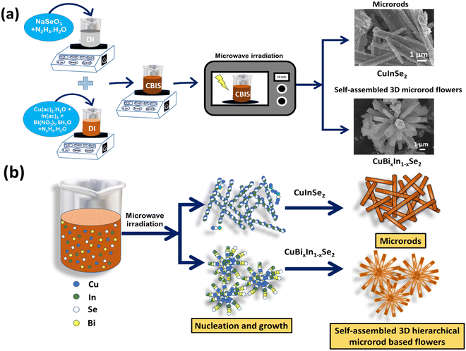 | ||
| Scheme 1 (a) Synthesis procedure and (b) possible growth process of microwave-assisted preparation of CBIS MFs. | ||
2.4. Characterizations
An XRD (Bruker D8 Advance diffractometer) was utilized for structural analysis using Cu Kα (λ = 1.54 Å) as an incident ray operating at 30 kV and 40 mA over the angular range 10°–70°. For surface morphological analysis, FESEM (JEOL, JSM-7601FPLUS) and transmission electron microscopy (TEM) (JEOL, TEM-7601FPLUS) instruments were used. The confirmation of elemental constituents and its mapping were carried out using an energy-dispersive X-ray spectroscopy (EDX) unit attached to the FESEM system. The Raman measurement was carried out using a Renishaw inVia Raman microscope (Model RE 04). Room-temperature PL measurements were carried out using a fluorometer attached to a Raman spectrometer at 532 nm excitation. An XPS (Axis Ultra Kratos Analytical, UK) instrument was used to analyze the change related to chemical structure–related modifications. The core-level XPS spectra were recorded with Al Kα X-rays (1486.6 eV) using a vacuum of 2 × 10⁻⁹ torr. Quantitative analysis of elements present in the sample was performed using an inductively coupled plasma mass spectrometer (ICP-MS) (Model-PerkinElmer optima 21000V). The optical study of the sample was measured from the absorbance data acquired using a UV-Vis-NIR spectrophotometer (Model – JASCO-660) at a wavelength in the range of 400–900 nm. The thermal behaviour of the sample was studied by differential scanning calorimetry (DSC) measurement (Model – DSC7020 (HITACHI)). The accuracy of heat flow is ± 0.01 mW and the heating rate is 10 °C min−1.2.5. Photo response measurement
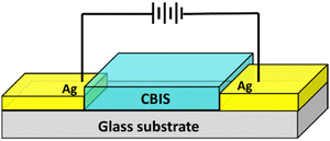
The photo response study of the CBIS samples was done by a drop casting technique using CBIS powder dispersed in 3 ml ethanol on a glass substrate on an area of 5 × 5 mm2. The cross-section SEM of the prepared film is presented in Fig. S1 (ESI†). The thickness of the film was found to be ∼54 μm. The deposited sample was mounted on a sample holder at room temperature. For conducting contact, a slight amount of silver paste was used in the two parallel edges of the deposited film presented in Scheme 2. The photo response measurement of the sample under dark and light conditions was taken under a 9 W white bulb over the sample. The current values over different voltages were measured using a Keithley 2450 Source Measure Unit in the voltage range of −10 V to 10 V with a step size of 0.03. For each sample, different measurements were carried out several times to confirm the reproducibility of the devices. Moreover, three different sets of drop-casted films were prepared and I–V measurement was repeated for each of the five cases.3. Results and discussion
3.1. MR/MF formation
CIS MRs and CBIS MFs were synthesized by a microwave-assisted synthesis method. This synthesis approach provides the advantages of shortening reaction time, improvement in product purity, and better control over size. Here, the transition from MRs to 3D MR-based flower architecture for different samples is observed in Scheme 1. The main reason includes microwave irradiation, concentration change, and usage of reducing agents during the process, which act as critical factors for the transformation. Microwave irradiation enables extremely rapid heating of dipoles and ions, compared to other conventional thermal techniques of heat transfer. During the process, microwave irradiation modulates functionality behaviors and dynamic reactions in the desired direction for nano/micro particle synthesis.30 Thus, this might be a possible reason for transformation. Various studies on size and morphology variation have been conducted by microwave-assisted synthesis methods.31,32In the current study, first using hydrazine hydrate as a reducing agent, Cu, Se, and In were converted into their ionic forms such as Cu2+, Se2−, and In3+ (in Scheme 1), and then the microwave-assisted heating reaction of Cu, In, and Se led to the formation of MRs. Further, providing the same heating condition through microwave, replacing Bi with Cu, In, and Se using the same reducing agent and varying the composition led to the formation of self-assembled MR-based flower architectures. Here, the formed MRs might act as nucleation centers for the formation of such 3D MFs. Furthermore, with the increase in Bi concentration, the synthesized product varies from CIS to CBIS, and its morphology varies from MRs to MFs. The greater atomic radius of Bi than that of others might be responsible for the increase in the size by forming these 3D hierarchical MFs. In another way, such transition in morphology primarily relies on the reducing agent used throughout the synthesis process. These reducing agents control the growth and bring many alterations in the material's morphological structure. In the current study, the conversion of MRs into 3D MFs might depend on the reaction during the synthesis process. The reactions among Cu, In, and Bi–hydrazine hydrate complexes, and the Se ions with the same are the prime reasons for the modification. Hydrazine hydrate as a reducing agent not only reduces the elements to their ionic forms but also integrates within the lattice to form a composite structure. This led to both single-structural evolution and multi-structure assembly and concurrent structural evolution.33,34 Thus, with hydrazine reduction, the microstructures significantly reconstruct themselves to form a flower structure by preserving the dimensional footprint while adding a fraction of volume.
3.2. Characterizations
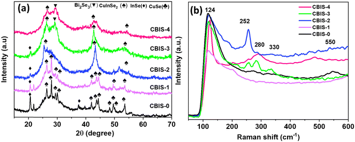
The structural change resulting from the compositional variation in CBIS MFs was analyzed from the XRD study. Fig. 1(a) depicts the XRD pattern for the respective samples, which revealed the polycrystalline nature with four distinct phases. The XRD pattern matching the respective ICSD data pattern is presented in Fig. S2 (ESI†). The peaks appearing at 26.50° (1 1 2), 41.67° (1 0 5), 41.87° (2 1 3), 44.10° (2 0 4), 47.69° (3 0 1), 48.78° (3 1 0), and 52.34° (3 1 2) present the CIS tetragonal phase (ICSD: 01-087-2265), which slightly loses its intensity with the increase in the Bi content. Similarly, the peak appeared at 21.23° (4 0 0) and 45.27° (0 0 2), corresponding to the InSe phase (ICSD: 00-012-0118) with a hexagonal crystal system. The InSe peak disappeared with both the increase in the Bi content and the decrease in In content. Additionally, the orthorhombic CuSe crystal structured pattern (ICSD: 00-027-0184) was observed at 27.86° (1 1 2), 29.80° (0 2 3), 30.97° (0 0 6), 45.18° (1 1 7), 49.67° (0 2 8), 49.85° (1 1 8), 55.90° (1 3 6), and 56.34° (2 0 6) respectively. The variation in Bi/In composition reduces the peak intensity of CuSe and InSe phases while increasing the broad hump intensity. With the increase in the Bi content, the appearance of a small peak at 29.28° (0 1 5) corresponding to the rhombohedral Bi2Se3 phase (ICSD: 00-033-0214) was observed, respectively. Incorporating bismuth with a larger atomic radius instead of indium causes a lattice mismatch within the matrix. This causes more defects and disorder within the system, as evidenced from the XRD spectral analysis, which led to a reduction in the optical band energy of the system. Additionally, the XRD pattern of reproduced samples is presented in Fig. S3(a) (ESI†), which showed a consistent pattern for all samples.The Raman spectra of the investigated samples are shown in Fig. 1(b). The spectra revealed four distinct peaks with different intensities at 124 cm−1, 252 cm−1, 280 cm−1, 330 cm−1, and 550 cm−1. The peak at 124 cm−1 could be attributed to the CIS system's single phase.35 The 252 cm−1 vibrational peak might be due to the CuSe longitudinal optic (LO) phonon mode due to Cu–Se vibrations.36 The 280 cm−1 vibrational peak corresponds to Cu2Se, respectively.37 The 330 cm−1 is assigned to the vibration of the BiO6 unit.38 The peak at 550 cm−1 corresponds to the Se chain that appeared due to second-order Raman scattering.39 The change in ternary phase intensity could be attributed to chemical bonding rearrangements caused by the change in composition, which alters the material's optical behaviour. The peak intensity variation as a function of Bi/In concentration indicates structural rearrangement within the matrix. Furthermore, it can be observed that with the increase in Bi content replacing In led to the formation of weaker and homopolar bonds, which satisfies the XRD study as it indicated the increment defects inside the system. These defects related to weaker bonds created localized states over the band gap region resulting in bandgap shrinkage.
The FESEM images of the as-prepared samples are shown in Fig. 2 and Fig. S4 (in ESI†). Fig. 2 shows the FESEM images of the CBIS-0 and CBIS-2 samples, which confirm the presence of MRs in the former and the formation of self-assembled 3D hierarchical MFs in the latter over three different magnification ranges. The clean proper MRs formed for the CBIS-0 sample with a diameter of 1.15 μm are shown in Fig. 2(a)–(c), whereas the 3D MFs formed by self-assembling MRs for the CBIS-2 sample are observed in Fig. 2(d)–(f). The small dot-like particles over the rods are precursors. The FESEM pictures of CBIS-1. CBIS-3 and CBIS-4 samples with different magnification ranges are presented in Fig. S4 (ESI†), which showed the formation of MFs with different magnifications. This dimension of MFs remains consistent with the Bi/In content change.
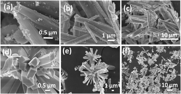 | ||
| Fig. 2 FESEM images of (a)–(c) CBIS-0 and (d)–(f) CBIS-2 samples under three different magnifications. | ||
Fig. 3 shows the mapping images and EDX spectra of the CBIS-2 sample. The EDX spectrum in Fig. 3(a) demonstrates the compositional analysis of the respective sample, confirming the presence of Cu, In, Se, and Bi elements in the material. The EDX spectra were recorded over various regions and confirmed uniformity over elemental composition. Fig. 3(b)–(f) show the elemental mapping images of the CBIS-2 sample, which includes Cu, In, Se, Bi, and elements, and the combined mapping image is shown in Fig. 3(f). The mapping images demonstrated the uniform distribution of elements throughout the prepared sample. For a better study of the elemental distribution, elemental mapping and EDX were performed in a specific region of the rods. The EDX spectra of other samples are shown in Fig. S5 (in ESI†), confirming the respective element's appearance. The elemental composition percentage is presented in Table S1 (ESI†), which showed ∼3% error in composition.
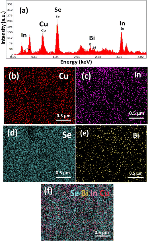 | ||
| Fig. 3 (a) EDX spectra and elemental mapping corresponding to (b) Cu, (c) In, (d) Se, and (e) Bi, and (f) merged mapping of the CBIS-2 MFs (Fig. 2(d)). | ||
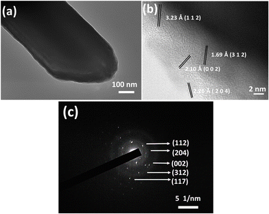
To get a clear picture of the morphology and crystalline property, the CBIS-2 sample was subjected to TEM imaging, and the results are presented in Fig. 4. Fig. 4(a) confirms the formation of a MR, whereas the appearance of a single rod with no flower structure is due to the dissociation of the rod flower during sonication. The high-resolution image (HRTEM) in Fig. 4(b) confirms the polycrystalline nature. The diffraction fringes observed having lattice spacings are ∼3.23 Å, 2.26 Å, are 1.69 Å, corresponding to the (1 1 2), (2 0 4), and (3 1 2) planes of the CIS phase, and ∼2.10 Å presents the InSe (0 0 2) plane respectively. In Fig. 4(c), the selected area electron diffraction (SAED) showed the existence of different fringes that represent different planes of CIS, InSe, and CuSe. The observed fringes corresponding to [1 1 2]. [2 0 4], and [3 1 2] represent the CIS tetragonal phase. Furthermore, the [0 0 2] and [1 1 7] planes correspond to the hexagonal phase of InSe and the orthorhombic crystal structure of CuSe. The observed diffraction fringes are also confirmed by the XRD and Raman study.
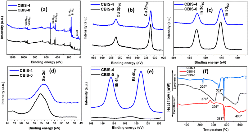
XPS measurement was carried out for the elemental composition analysis and determining the elemental binding states of MFs. The XPS study was carried out for CBIS samples and the corresponding spectra are presented in Fig. 5. The XPS survey spectrum in Fig. 5(a) of samples confirms the presence of Cu, In, Se, and Bi elements by peaks representing Cu 2p, In 3d, Se 3d, and Bi 4f. Copper showed valence state +1 by forming the CIS phase in Fig. 5(b) and exhibited two high-resolution peaks corresponding to Cu 2p1/2 and Cu 2p3/2 at 932.32 and 950.89 eV, respectively.3,40 No significant peak shifting and satellite peaks were observed in the Cu peak position. Fig. 5(b) presents the high-resolution spectra of In 3d with a peak positioned at 451. 62 eV and 443.87 eV corresponding to 3d5/2 and 3d3/2 core shells. It confirms the exhibition of In valence state +3, and no significant shifting was observed.41,42 However, both high-resolution spectra of In showed reduced intensity in CBIS-4 compared to CBIS-0, which might be due to the significant change in the stoichiometry that occurred, which led to bonding rearrangements. Similarly, the Se 3d spectrum in Fig. 5(d) showed a broad peak at 54.34 eV, confirming the valence state −2.43 it can be observed that with Bi addition, slight shifting is observed towards a lower binding energy (∼0.2 eV), which might be due to the bonding arrangement with Bi addition. Fig. 5(e) presents the spin–orbit splitting of 4f Bi into 4f7/2 and 4f5/2, positioned at 157.43 eV and 163.60 eV. The absence of Bi peaks in the primary sample CBIS-0 and the presence of the same in the CBIS-4 sample confirm the Bi content variation.44 Doping led to significant defect redistribution. Thus, it can be observed that with Bi addition, the peak intensity is reduced, possibly due to the creation of defects and disorder inside the system. In other words, since the XPS signal is extremely surface sensitive and decays exponentially with depth, the reduction in intensity suggests that the doping causes vacancies and interstitials due to lattice mismatch, which reduced intensity.45,46 Furthermore, the XPS elemental composition of CBIS-0 and CBIS-4 samples is depicted in Table S1 (ESI†), confirming the presence of the respective elements. To provide additional clarity on the chemical composition of CBIS, quantitative elemental analysis of one sample (CBIS-4) was conducted using ICP-MS, and the results are presented in Table S1 (ESI†). The elemental concentrations obtained from EDX, XPS, and ICP-MS were found to be closely aligned with each other. However, in CBIS-4, the ICP-MS data for Se concentration showed a slight reduction compared to other two, attributed to the H2Se loss during sample preparation.
The DSC experiments were performed for three samples, CBIS-0, CBIS-2, and CBIS-4, presented in Fig. 5(f) to analyse the change in thermal response. The samples were performed DSC study in scanning rates of 10 °C min−1, which yielded endothermic and exothermic peaks for the samples. The experiments were done in the temperature range of 30–550 °C. Table 1 summarizes the peaks and the change in the amount of heat flows. The sample CBIS-0 comprised three endothermic peaks at 309 °C, and 378 °C presenting the decomposition of Cu11In9 and CuSe.47 The primary peak at 309 °C is associated with the peritectic decomposition of Cu11In9,48 whereas the peak at 378 °C corresponds to CuSe partial decomposition (2CuSe → βCu2−xSe + Seliq).47,48 An endothermic peak near 493 °C cannot be accounted for with any phase transitions in the system. According to the In–Se binary system, a possible reaction due to In3Se4 occurs near 500 °C, and the XRD analysis fails to support this hypothesis.47,49 The 276 °C exothermic peak might be associated with the formation of In4Se3 and InSe. Assigning them to one reaction is difficult since various reactions occur simultaneously.48 The above-mentioned peaks with pronounced intensity also appeared in the CBIS-2 and CBIS-4 samples. However, in the case of CBIS-4, the 309 °C peak merged with an additional endothermic peak at 332 °C, corresponding to the decomposition of CuSe2 (CuSe2 → CuSe + Seliq).47,48 Peak at 220 °C appeared in the CBIS-4 sample and is absent in other samples most probably due to the melting of elemental selenium trapped within CIS. The absence of a selenium melting peak might be due to easier partial consumption due to the formation of CuSe. Therefore, the more easily accessible the Se element, the easier it is to form CuSe.47
| Sample | Endothermic | Exothermic | ||
|---|---|---|---|---|
| Temperature (°C) | Enthalpy (J g−1) | Temperature (°C) | Enthalpy (J g−1) | |
| CBIS-0 | 309 | 15.88 | 276 | −12.95 |
| 378 | ||||
| 493 | ||||
| CBIS-2 | 310 | 20.96 | — | — |
| 378 | ||||
| 490 | ||||
| CBIS-4 | 309 | 27.68 | — | — |
| 332 | ||||
| 378 | ||||
| 492 | ||||
3.3. Optical properties
The absorbance behaviour of CBIS MFs with different Bi/In contents is shown in Fig. 6(a). The absorbance increases as the Bi content increases in place of In. This behaviour is due to the greater atomic radius of Bi, which led to densification inside the matrix, thereby increasing the absorbance. The absorbance of the second set CBIS samples is presented in Fig. S3(b) (ESI†), showing a consistent nature for all samples. The CBIS MFs have a high absorbance over the visible region, indicating their potential for photovoltaic applications.34 The optical bandgap of the studied samples was estimated by taking the absorption coefficient, presented as, , where ‘d’ presents the sample's thickness (d = 1 cm cuvette thickness), and ‘T’ presents the sample's transmittance observed over varying wavelength ranges. The material's optical bandgap (Eg) of a semiconductor is an important optical parameter that explains the photon energy required to excite an electron from the valence band to the conduction band. It is a fundamental characteristic that deliberates the material's electronic structure with the corresponding potential device applications in different fields such as optoelectronics and solar cells. In particular, the small bandgap is desired for enhancing the PV solar cell efficiency. However, the PV absorption capacity directly correlates with the electronic structure of materials and is considered the major aspect of calculating the optical Eg.50 In the high absorption regime (α ≥ 104 cm−1) of the amorphous materials, the absorption edge follows the Tauc relation:51
| αhν = B(hν − Eg)1/2 | (1) |
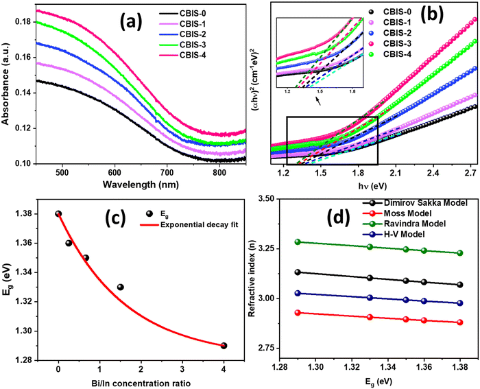 | ||
| Fig. 6 (a) Absorbance, (b) (αhν)2vs. hν variation, (c) variation in Eg with the Bi/In concentration ratio, and (d) refractive indices using different models of different CBIS MFs. | ||
| Optical constants | CBIS-0 | CBIS-1 | CBIS-2 | CBIS-3 | CBIS-4 | |
|---|---|---|---|---|---|---|
| Optical bandgap (eV) | 1.38 | 1.36 | 1.35 | 1.33 | 1.29 | |
| linear refractive index (n) | D–S model | 3.069 | 3.082 | 3.089 | 3.103 | 3.132 |
| Ravindra model | 3.228 | 3.240 | 3.247 | 3.259 | 3.284 | |
| H–V model | 2.977 | 2.988 | 2.993 | 3.004 | 3.027 | |
| Moss model | 2.880 | 2.890 | 2.896 | 2.907 | 2.929 | |
The refractive index, ‘n’, is the most significant parameter that plays an important role in optical Investigation. This parameter can be estimated and correlated using various well-known models using the material's energy gap. The ‘n’ of all synthesized samples was determined using the Eg values from the ‘Dimitrov and Sakka empirical formula’:57
 | (2) |
The estimated values of static linear refractive index for the films considering bandgap values are shown in Table 1. The estimated values showed an enhancement with the increase in the Bi content.
Furthermore, according to Ravindra et al.,58 ‘n’ was also calculated using the following relation:
| n = 4.084 − 0.62 Eg | (3) |
According to Herve and Vandamme,59 ‘n’ is related to Eg by following the formula which is consistent over 2.00 eV < Eg < 4.00 eV, given as follows:
 | (4) |
Table 2 shows the calculated refractive indices using the four above-mentioned models. In this case, the calculated energy bandgap values range from 1.39 to 1.29 eV, indicating that the estimated refractive index values based on these models are valid. It should be noted that ‘n’ for all models exhibits the same pattern of refractive index with Eg. ‘n’ clearly increases as the Bi content increases. This behavior predicts an increase in absorption capability, which increases electronic polarizability. Fig. 6(d) shows the variation in refractive index using various models for all samples. These four model's estimated refractive indices show the same pattern and are close to each other.
The PL emission (λex = 532 nm) spectra for all synthesized CBIS MFs with different Bi contents are presented in Fig. 7. A broad PL spectrum in the 550–950 nm range is observed for each case, with the main peak centered at 650–750 nm. It was clearly demonstrated that as the Bi content increased, the emission band shifted towards a higher wavelength region. This might be due to the enhancement of MR size and thickness by forming a flower cluster. This behavior also satisfies the decrease in bandgap and the increase in absorbance with the Bi content. The emission FWHM became narrower with the Bi content, which was also reflected in the other optical characteristics. However, the intensity of CBIS-4 decreased significantly, showcasing an abrupt pattern as the wavelength shifted. It is possibly due to the high Bi content, which increases the density of localized states over the bandgap region by creating more defects and disorder inside the matrix.61 Elaborately, the addition of Bi into CIS creates additional donor/acceptor levels over the forbidden gap region depending on the substitution of ‘Bi’ at the ‘In’ lattice site or interstitial sites. This led to multiple allowed transitions, as observed from PL analysis.
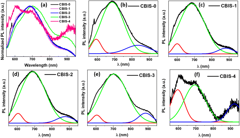 | ||
| Fig. 7 (a) Normalized PL spectra and (b)–(f) deconvoluted PL spectra of all CBIS MFs at 532 nm excitation. | ||
In Fig. 7(b)–(f), each spectrum's deconvolution showed a contribution from three Gaussian peaks. These three deconvoluted spectra at 610, 725, and 800 nm represent different emissive states. On the basis of stoichiometry, the relevant transitions corresponding to these deconvoluted peaks could be due to band-to-band and donor–acceptor-pair transitions. The visible emission was primarily caused by surface defects associated with Cu, In, and Se interstitial and vacancy sites.61,62 Surface states primarily determine the intensity of visible emission. The intense visible peak in the PL spectrum at room temperature indicates that the matrix has a large surface area and a large number of surface states.63
3.4. Photo response
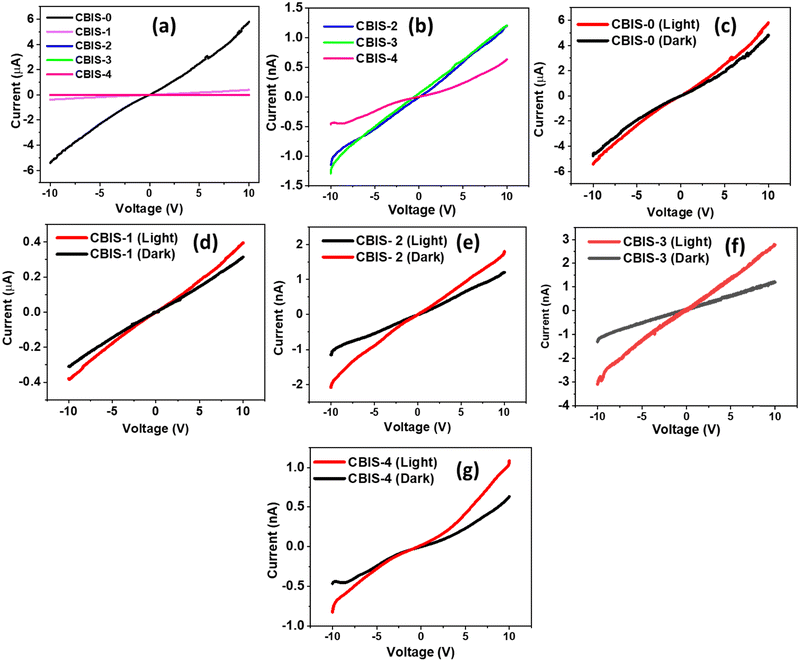
The current–voltage measurement of all CBIS samples were done by illuminating a 9 W white LED bulb and varying the dc voltage at room temperature. The I–V characteristics of devices based on all CBIS samples were obtained under both dark and illumination conditions, and the same is shown in Fig. 8. Measurements were carried out multiple times and, there is no significant difference in the observed data. Hence, one set of the data is provided in Fig. 8. It shows the qualitative features of the room-temperature dark current (ID) and light current (IL) of all CBIS samples (in Fig. 8(b)–(f)) with different Bi/In contents. In this figure, the current increased with the increase in voltage confirming ohmic nature.64,65 It is quite obvious from the observation that the photocurrent of the device based on the synthesized CBIS materials is significantly improved under illumination conditions from dark conditions.29,66,67 The maximum photocurrent under dark and light conditions for all samples is presented in Table 3, respectively. It is clearly observed from the table that the photocurrent gradually reduced with the increase in Bi content, replacing In content simultaneously. Such behaviour might be due to the increase in the defect's concentration and densification inside the material with Bi addition, which inhibited the electron flow and thereby reduced the photocurrent. The observed photocurrent in CBIS-0 (CuInSe2) case is ∼μA range, which satisfies other studies.68,69 It clearly illustrated the photocurrent for the CBIS-0 sample showed in the μA range, whereas the change in the Bi/In concentration led to a reduction in the photocurrent value to nA range (very less). Such behavior might be contributed from the increment in structural defects such as point defects (interstitial and vacancy). These structural defects might produce trap centers, which greatly affect the recombination of carriers. In other words, substituting Bi3+ into the CIS lattice results in the formation of acceptor energy levels over the forbidden gap. The free electrons available and generated due to illumination might get trapped at BiIn sites or recombine with holes available in the valence band, resulting in reduced carrier concentration, thereby reducing the photocurrent value.70,71 Thus, with the increase in Bi doping content, the photocurrent reduced from μA to nA range. This behavior is also correlated with the increase in resistance due to doping. Additionally, the morphological transition from MRs to 3D micro rod flower-like architects, causing a lower surface area-to-volume ratio, reduces the surface effects. Thus, it led to a reduction in the photocurrent response of the material with doping.56 There is no significant change observed in the I–V data of the second set of CBIS samples (Fig. S6(a)–(e), ESI†). This shows high reproducibility of the CBIS materials under both light and dark conditions, emphasizing the suitability for device applications.| Sample | Maximum photocurrent (Imax) in amp. at +10 V | Resistance (Ω) | |
|---|---|---|---|
| Light | Dark | ||
| CBIS-0 | 5.823 × 10⁻⁶ | 4.741 × 10⁻⁶ | 0.328 × 10⁷ |
| CBIS-1 | 3.953 × 10⁻⁷ | 3.186 × 10⁻⁷ | 0.231 × 10⁸ |
| CBIS-2 | 1.803 × 10⁻⁹ | 1.211 × 10⁻⁹ | 0.572 × 10¹⁰ |
| CBIS-3 | 2.814 × 10⁻⁹ | 1.271 × 10⁻⁹ | 0.352 × 10¹⁰ |
| CBIS-4 | 1.060 × 10⁻⁹ | 6.368 × 10⁻¹⁰ | 0.764 × 10¹⁰ |
Fig. 9 displays the current–time characteristics of three synthesized samples (CBIS-0, CBIS-2, and CBIS-4). A constant voltage of 7.5 V was applied across all cases to observe significant changes between light and dark conditions, each lasting for a 300-second interval. As shown in the figure, when the light was turned on, the photocurrent sharply increased due to the increase in carrier drift velocity. Fig. 9(a) and (b) illustrate the I–T response of CBIS-0 under white light in both light and dark conditions, showing an increase in photocurrent during illumination and a decrease in the darkness. The corresponding Ion and Ioff values are presented in Table S2 (ESI†). The Ion value under light conditions reaches 5.77 μA, while in the absence of light, If reduced to 5.03 μA (rise time) and 5.18 μA (fall time). The inconsistency in the peak photocurrent values for these materials is attributed to a higher concentration of defects and disorders. Nevertheless, a consistent bending at the transition is observed in each case, indicating the suitability of the devices for dynamic applications. Similar patterns are observed for CBIS-2 (Fig. 9(c) and (d)) and CBIS-4 (Fig. 9(e) and (f)). The results affirm a decrease in photocurrent from μA to nA with the increase in Bi concentration. Under the light condition, Ion reaches 1.57 nA (CBIS-2) and 0.99 nA (CBIS-4), while in the absence of light, Ioff decreases to 0.51 nA (CBIS-2) and 0.59 nA (CBIS-4) (rise time), and 0.59 nA (CBIS-2) and 0.92 nA (CBIS-4) (fall time). The I–T results for all three devices exhibit a sharp increase with light, attributed to continuous carrier generation under irradiation. Upon turning off the light, a slight abrupt decay in photocurrent is observed, attributed to recombination between trap carriers and injected free carriers. Additionally, distinct transient photocurrent characteristics are linked to non-radiative pathways and variations in carrier transport ability.72
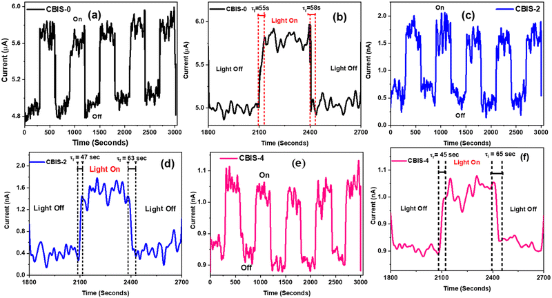 | ||
| Fig. 9 Current vs. time response and transient switching photo response curve of (a) and (b) CBIS-0, (c) and (d) CBIS-2, and (e) and (f) CBIS-4 samples. | ||
In the absence of illumination, the current is reduced to attain the initial value of current showing persistent nature. The rise response time, denoted by τr, represents the duration for the photocurrent to reach its peak (0–80%), while the fall time, denoted by τf, signifies the time taken for the reduction from the peak (100–20%).73 Specifically, τr reflects the time taken by the device to detect and respond to incident light, and τf indicates how quickly the device returns to its original state after the light source is turned off. The variations in both τr and τf are presented in Table S2 (ESI†) and illustrated in Fig. S7(a) (ESI†). For CBIS-0, the rise and decay times are 55 s and 58 s, respectively. In the case of CBIS-2, these times are 47 s and 63 s, and for CBIS-4, they are 45 s and 65 s. The longer response times may be attributed to increased defects and disorder within the system, probably a result of thermal effects. The carrier concentration is temperature dependent, and as the temperature rises, the current slightly varies with higher values due to increased carrier concentrations.74 The observed pattern illustrates a rapid rise and slow fall in current with each light cycle. The abrupt increase from the dark current level and subsequent gradual rise with illumination indicate the generation of free carriers from absorbed light energy. Notably, it is evident that τr decreases and τf increases with the increase in Bi concentration. Such behavior might be due to the defects and impurities inside the channel, which induced an extra energy level, affecting the relaxation behavior. Additionally, for better understanding, the Ion/Ioff ratio at rise and decay time is plotted in Fig. S7(b) (ESI†). The Ion/Ioff ratio variation during the rise time is more pronounced than during the fall time for all samples, with CBIS-2 exhibiting the highest variation, indicating superior responsivity to detector applications.75
Additionally, to demonstrate their stability over time, the time-dependent response of all three sample-based PDs was measured under white light at a bias voltage of 7.5 V. Fig. S8 (ESI†) presents the photocurrent stability under both light and dark conditions over 3000 seconds. The results confirmed that the response of these materials remains constant with tiny fluctuations. Nonetheless, these materials exhibited excellent stability at room temperature under light and dark conditions.
Furthermore, the resistance of all samples was calculated by using the inverse slope of the I–V curve,76,77 which is presented in Fig. S9 (ESI†). The resistance of the film is strongly dependent on the Bi/In composition variation. The calculated values of resistance enhanced with the Bi concentration in the CBIS matrix. The calculated values of resistance form the inverse slope of I–V plot are presented in Table 3. With the increase in Bi content, the resistance enhanced from 0.3264 × 10⁷ Ω to 0.7646 × 10¹⁰ Ω. Such increment in resistance might be due to impurities, which cause trap states, increase recombination and reduce mobility.78
4. Conclusion
BixCuIn1−xSe2 MFs have been prepared by a microwave-assisted synthesis method with non-toxic precursor chemicals. The polycrystalline nature was confirmed by an XRD study. XPS and the Raman study observed the structural alteration induced by compositional variation among Bi/In. The morphological study showed the transition from microrods to self-assembled 3D hierarchical MR-based flower architectures with uniformity over the shape and size of the structure formed. Moreover, the change in Bi/In composition in the host lattice results in the formation of the more localised states, which is represented by the defects and disorder with a lower band energy within the forbidden gap. The incorporation of bismuth led to enhancement in absorption capability over the visible range. The PL reflected the same response by shifting towards a higher wavelength over the visible range. Each broad spectrum is contributed from three deconvoluted peaks corresponding to the transition among localized states. The compositional change led to endothermic and exothermic processes inside the system. The current–voltage response showed a reduction in photocurrent from the μA range to the nA range with composition variation. Additionally, the photocurrent response with time showed good stability, which facilitates their application in photodetection.Conflicts of interest
There are no conflicts to declare.Acknowledgements
The author Dr R. Naik thanks the central instrumentation facility of ICT-IOC for different characterizations and Science and Engineering Research Board, Govt. of India for financial support (CRG/2022/003084-G).References
- B. M. Palve, C. V. Jagtap, V. S. Kadam, C. D. Lokhande and H. M. Pathan, Eng. Sci., 2020, 12, 52–76 CAS.
- W. Lian, D. Tu, P. Hu, X. Song, Z. Gong, T. Chen, J. Song, Z. Chen and X. Chen, Nanotoday, 2020, 35, 100943 CrossRef CAS.
- P. Priyadarshini, S. Senapati, S. Bisoyi, S. Samal and R. Naik, J. Alloys Compd., 2023, 945, 169222 CrossRef CAS.
- K. Jain, S. Kishor, K. S. Singh, M. Odelius and L. M. Ramaniah, J. Phys. Chem. C, 2021, 125(49), 27046–27057 CrossRef CAS.
- B. F. Goncalves, A. P. Lagrow, S. Pyrlin, B. O. Baird, G. Botelho, L. S. A. Marques, M. M. D. Ramos, K. Kovnir, S. L. Mendez and Y. V. Kolenko, Nanomaterials, 2021, 11(5), 1148 CrossRef CAS PubMed.
- K. Benameur, Y. Mouchaal, K. Benchouk, A. Laafer and R. Barille, Inorg. Chem. Commun., 2022, 136, 109165 CrossRef CAS.
- I. N. Odin, M. V. Gapanovich, M. V. Chukichev and G. F. Novikov, Mendeleev Commun., 2020, 30, 666–668 CrossRef CAS.
- F. Li, M. Zhang, D. Benetti, L. Shi, L. V. Besteiro, H. Zhang, J. Liu, G. S. Selopal, S. Sun, Z. Wang, Q. Wei and F. Rosei, Appl. Catal., 2021, 280, 119402 CrossRef CAS.
- B. Luo, J. Liu, H. Guo, X. Li, R. Song, K. Shen, Z. M. Wang, D. Jing, G. S. Selopal and F. Rosei, Nano Energy, 2021, 88, 106220 CrossRef CAS.
- M. Mohammadnezhad, M. Liu, G. S. Selopal, F. N. Parda, Z. M. Wang, B. Stansfield, H. Zhao, C. Y. Lai, D. R. Radu and F. Rosei, Electrochim. Acta, 2020, 340, 135954 CrossRef CAS.
- J. Kazmi, P. C. Ooi, B. T. Goh, M. K. Lee, M. F. Mohd, R. Wee, S. S. A. Karim, S. R. A. Raza and M. A. Mohamed, RSC Adv., 2020, 10, 23297–23311 RSC.
- M. Jafarzadeh, C. S. Sipaut, J. Dayou and R. F. Mansa, Renewable Sustainable Energy Rev., 2016, 64, 543–568 CrossRef CAS.
- M. A. S. Andrade Jr. and L. H. Mascara, MRS Commun., 2018, 8, 504–508 CrossRef.
- M. A. S. Andrade Jr. and L. H. Mascara, Chemosphere, 2018, 212, 79–86 CrossRef PubMed.
- M. Shkir, K. V. Chandekar, A. Khan, A. M. El-Toni and S. Alfaify, Mater. Sci. Semicond. Process., 2020, 107, 104807 CrossRef CAS.
- L. P. Chikhale, J. Y. Patil, F. I. Shaikh, A. V. Rajgure, R. C. Pawar, I. S. Mulla and S. S. Suryavanshi, Mater. Sci. Semicond. Process., 2014, 27, 121–129 CrossRef CAS.
- S. Das, P. Priyadarshini, S. Senapati, S. Bisoyi, S. K. Samal and R. Naik, J. Alloys Compd., 2023, 960, 170999 CrossRef CAS.
- S. Paul and S. K. Pradhan, Mater. Today: Proc., 2022, 66, 1269–1274 Search PubMed.
- Y. Zhang, Y. Yang, Z. Hou, X. Jiang, L. Zhang, Y. Yang and Y. Wang, AIP Adv., 2020, 10, 035313 CrossRef CAS.
- S. Sugan, K. Baskar and R. Dhanasekaran, Curr. Appl. Phys., 2014, 14, 1416–1420 CrossRef.
- J. Tang, S. Hinds, S. O. Kelley and E. H. Sargent, Chem. Mater., 2008, 20(22), 6906–6910 CrossRef CAS.
- M. Saylan, B. Mertin, H. Akbiyik, F. Turak, G. Cetin and S. Bakirdere, J. Food Compos. Anal., 2023, 115, 104965 CrossRef CAS.
- C. C. Wu, C. Y. Shiau, D. W. Ayele, W. N. Su, M. Y. Cheng, C. Y. Chiu and B. J. Hwang, Chem. Mater., 2010, 22(14), 4185–4190 CrossRef CAS.
- Y. H. Seo, B. S. Lee, Y. Lo, H. G. Kim, Y. Choi, S. J. Ahn, K. H. Yoon, K. Woo, J. Moon, B. H. Ryu and S. Jeong, J. Phys. Chem. C, 2013, 117(19), 9529–9536 CrossRef CAS.
- R. P. Oleksak, B. T. Flynn, D. M. Schut and G. S. Herman, Phys. Status Solidi, 2014, 211, 219–225 CrossRef CAS.
- H. Grisaru, O. Palchik, A. Gedanken, V. Palchik, M. A. Slifkin and A. M. Weiss, Inorg. Chem., 2003, 42, 7148–7155 CrossRef CAS PubMed.
- J. Wang, Y. Cui and D. Wang, Adv. Mater., 2019, 31(38), 1801993 CrossRef PubMed.
- W. Zhou, Z. Yin, D. H. Sim, H. Zhang, J. Ma, H. H. Hng and Q. Yang, Nanotechnology, 2011, 22(19), 195607 CrossRef PubMed.
- M. S. Alam, M. N. Javed, F. H. Potto, A. Waziri, F. A. Almalki, M. S. Hasnain, A. Garg and M. K. Saifullah, Appl. Organomet. Chem., 2019, 33, e5071 CrossRef.
- J. Wojnarowicz, T. Chudoba, I. Koltsov, S. Gierlotka, S. Dworakowska and W. Lojkowski, Nanotechnology, 2018, 20, 065601 CrossRef PubMed.
- E. Mohammadi, A. Aliofkhazraei, M. Hasanpoor and M. Chipara, Crit. Rev. Solid State Mater. Sci., 2018, 43, 475–541 CrossRef CAS.
- X. Medvedeva, A. Vidyakina, F. Li, A. Mereshchenko and A. Klinkova, Nanomaterials, 2019, 9, 1445 CrossRef CAS PubMed.
- S. Das, S. Senapati, G. K. Pradhan, S. Varadharajanperumal and R. Naik, ACS Appl. Nano Mater., 2023, 6(7), 5298–5312 CrossRef CAS.
- M. Latha, R. A. Devi and S. Velumani, Opt. Mater., 2018, 79, 450–456 CrossRef CAS.
- E. P. Zaretskaya, V. F. Gremenok, V. Riede, W. Schmitz, K. Bente, V. B. Zalesski and O. V. Ermakov, J. Phys. Chem. Solids, 2003, 64, 1989–1993 CrossRef CAS.
- O. Ramdani, J. F. Goillemoles, D. Lincot, P. P. Grand, E. Chassaing, O. Kerrec and E. Rzepka, Thin Solid Films, 2007, 515, 5909–5912 CrossRef CAS.
- I. L. Li, J. P. Zhai, P. Launois, S. C. Ruan and Z. K. Tang, J. Am. Chem. Soc., 2005, 127, 16111–16119 CrossRef CAS PubMed.
- D. Kasprowicz, T. Runka, K. Jaroszewski, A. MMajchrowski and E. Micalski, J. Alloys Compd., 2014, 610, 600–605 CrossRef CAS.
- K. Kaur, Nisika, A. H. Chwdhury, Q. Qiao and M. Kumar, J. Alloys Compd., 2021, 854, 157160 CrossRef CAS.
- D. Sahoo, S. Senapati, S. Samal, S. Varadharajaperumal and R. Naik, ACS Appl. Eng. Mater., 2023, 1(3), 1001–1012 CrossRef CAS.
- S. Senapati, A. Rath and K. K. Nanda, Appl. Phys. A: Mater. Sci. Process., 2018, 124, 61 CrossRef.
- S. Senapati and K. K. Nanda, ACS Appl. Mater. Interfaces, 2015, 7(42), 23481–23488 CrossRef CAS PubMed.
- S. Li, R. Ma, C. Ma, K. Huang, D. Li, Y. Xian, L. He and H. Zhu, Mater. Lett., 2013, 101, 51–53 CrossRef CAS.
- P. Priyadarshini, S. Das, S. Senapati, S. K. Samal, G. K. Pradhan and R. Naik, Surf. Interfaces, 2023, 37, 102687 CrossRef CAS.
- D. W. Houck, E. I. Assaf, H. Shin, R. M. Greene, D. R. Pernik and B. A. Korgel, J. Phys. Chem. C, 2019, 123, 9544–9551 CrossRef CAS.
- J. J. Wang, Y. Q. Wang, F. F. Cao, Y. G. Guo and L. J. Wan, J. Am. Chem. Soc., 2010, 132(35), 12218–12221 CrossRef CAS PubMed.
- A. Gobeaut, L. Laffont, J. M. Tarascon, L. Parissi and O. Kerrec, Thin Solid Films, 2009, 537, 4436–4442 CrossRef.
- K. Tang, U. Kunecke, F. Oehlsclager, A. Holzing, R. Schurr, R. Hock and P. W. Wellmann, Sol. Energy Mater. Sol. Cells, 2010, 94, 1875–1879 CrossRef CAS.
- H. Okamoto, J. Phase Equilib. Diffus., 2004, 25, 201 CrossRef CAS.
- M. M. Rhaman, M. A. Matin, M. A. Hakim and M. F. Islam, Mater. Sci. Eng., B, 2021, 263, 114842 CrossRef CAS.
- A. Parida, S. Senapti, G. K. Pradhan and R. Naik, J. Alloys Compd., 2023, 970, 172520 CrossRef.
- R. S. Kumar, B. D. Ryu, S. Chandramohan, J. K. Seol, S. W. Lee and C. H. Hong, Mater. Lett., 2012, 86, 174–177 CrossRef.
- A. I. A. Salam, M. M. Awad, T. S. Soliman and A. Khalid, J. Alloys Compd., 2022, 898, 162946 CrossRef.
- S. V. Desarada, K. B. Chavan and N. B. Chaure, J. Electron. Mater., 2023, 52, 3413–3419 CrossRef CAS.
- X. Li, X. Tong, S. Yue, C. Liu, A. I. Channa, Y. You, R. Wang, Z. Long, Z. Zhang, Z. Zhao, X. F. Liu and Z. M. Wang, Nano Energy, 2021, 89, 106392 CrossRef CAS.
- V. Postica, M. Hoppe, J. Grottrup, P. Haves, V. Robisch, D. Smazna, R. Adelung, B. Viana, P. Aschehoug, T. Pauporte and O. Lupan, Solid State Sci., 2017, 71, 75–86 CrossRef CAS.
- M. N. Azlan, M. K. Halimah, S. Z. Shafinas and W. M. Daud, Mater. Express, 2015, 5, 211–218 CrossRef.
- N. M. Ravindra, S. Auluck and V. K. Srivastava, Phys. Status Solidi B, 1979, 93, K155 CrossRef CAS.
- P. J. L. Herve and L. K. J. Vandamme, J. Appl. Phys., 1995, 77, 5476–5477 CrossRef CAS.
- T. S. Moss, Proc. Phys. Soc., London, Sect. B, 1950, 63, 167 CrossRef.
- J. E. Lee, H. Lee, D. S. Jeong, B. Pejjai, V. R. M. Reddy and C. Park, Chin. J. Phys., 2018, 56, 392–403 CrossRef CAS.
- M. Fu, W. Luan, S. T. Tu and L. Mleczko, Green Process. Synth., 2017, 6, 133–146 CrossRef CAS.
- I. Shalish, H. Temkin and V. Narayanamurti, Phys. Rev., 2004, 69, 1–4 Search PubMed.
- R. Guo, J. Meng, W. Lin, A. Liu, T. Pullerits, K. Zheng and J. Tian, Chem. Eng. J., 2021, 403, 126452 CrossRef CAS.
- E. Aslan and M. Zarbali, Opt. Mater., 2022, 125, 112030 CrossRef CAS.
- G. Regmi, A. Ashok, P. Chawla, P. Semalti, S. Velumani, S. N. Sharma and H. Castaneda, J. Mater. Sci.: Mater. Electron., 2020, 31, 7286–7314 CrossRef CAS.
- V. R. Voggu, J. Sham, S. Pfeffer, J. Pate, L. Fillip, T. B. Harvey, R. M. Brown and B. A. Korgel, ACS Energy Lett., 2017, 2(3), 574–581 CrossRef CAS.
- D. S. I. Jebakumar, B. Chitara and S. B. Krupanidhi, J. Nanosci. Nanotechnol., 2017, 17(2), 1538–1542 CrossRef PubMed.
- G. Karmakar, A. Tyagi, A. Wadawale, G. Kedarnath, A. P. Srivastava, C. A. Betty and V. Singh, ChemistrySelect, 2018, 3(37), 10394–10401 CrossRef CAS.
- C. Y. Chang, J. Shieh, Y. L. Kuo, J. Y. Guo, S. Y. Chen and C. L. Kuo, Appl. Surf. Sci., 2023, 638, 158018 CrossRef CAS.
- K. Kairajan, A. N. A. Anasthasiya, O. A. Aldossary, M. Ubaidullah and M. Karunakaran, Sens. Actuators, A, 2021, 319, 112531 CrossRef.
- T. Wang, T. Fang, X. Li, L. Xu and J. Song, J. Phys. Chem. C, 2021, 125(10), 5475–5484 CrossRef CAS.
- V. Bhatt, M. Kumar, E. C. Kim and H. J. Chung, J. Alloys Compd., 2022, 922, 166190 CrossRef CAS.
- T. Jiang, Y. Zang, H. Sun, X. Zheng, Y. Liu, Y. Gong, L. Fang, X. Cheng and K. He, Adv. Opt. Mater., 2017, 5, 1600727 CrossRef.
- R. Guo, T. Shen and J. Tian, J. Mater. Chem. C, 2018, 6, 2573–2579 RSC.
- A. Parida, S. Senapati, S. Samal, S. Bisoyi and R. Naik, ACS Appl. Nano Mater., 2023, 6, 11230–11241 CrossRef CAS.
- M. Devika, N. K. Reddy, K. Ramesh, K. R. Gunasekhar, E. S. S. R. Gopal and K. T. R. Reddy, J. Electrochem. Soc., 2006, 153, 727 CrossRef.
- M. Hashemi, S. M. B. Ghorashi, F. Tajabadi and N. Taghavinia, Mater. Sci. Semicond. Process., 2021, 126, 105676 CrossRef CAS.
Footnote |
| † Electronic supplementary information (ESI) available. See DOI: https://doi.org/10.1039/d3tc03250g |
| This journal is © The Royal Society of Chemistry 2024 |

