 Open Access Article
Creative Commons Attribution 3.0 Unported Licence
Electroanalytical overview: the use of laser-induced graphene sensors
Robert D.
Crapnell
 a,
Elena
Bernalte
 a,
Rodrigo A. A.
Muñoz
 b and
Craig E.
Banks
 *a
*a
aFaculty of Science and Engineering, Manchester Metropolitan University, Dalton Building, Chester Street, Manchester, M1 5GD, UK. E-mail: c.banks@mmu.ac.uk; Tel: +44-(0)-161-247-1196
bInstitute of Chemistry, Federal University of Uberlândia, Uberlândia, 38400-902, Minas Gerais, Brazil
First published on 9th December 2024
Abstract
Laser-induced graphene, which was first reported in 2014, involves the creation of graphene by using a laser to modify a polyimide surface. Since then, laser-induced graphene has been extensively studied for application in different scientific fields. One beneficial approach is the use of laser-induced graphene coupled with electrochemistry, where there is a growing need for disposable, conductive, reproducible, flexible, biocompatible, sustainable, and economical electrodes. In this mini overview, we explore the use of laser-induced graphene as the basis of electroanalytical sensors. We first introduce laser-induced graphene, before moving to the use of laser-induced graphene electrodes highlighting the various approaches and different laser parameters used to produce different graphene micro and macro structures, whilst describing how these structures are characterised and benchmarked for those working in the field of laser-induced graphene electrodes for comparison aspects. Next, we turn to the use of laser-induced graphene electrodes as the basis of electrochemical sensing platforms towards key analytes and its use in the development of biosensors. We provide a critical overview of the use of laser-induced graphene sensors compared to screen-printed and additive manufactured electrodes, providing future suggestions for the field.
Introduction to laser-induced graphene
Graphene is a unique material which is composed of a single layer of carbon atoms within a hexagonal honeycomb lattice. It exhibits advantageous properties of improved thermal, mechanical, optical, and electrical transport, resulting in it being explored in a range of applications.1–3 There are many ways to produce graphene, which include micromechanical and liquid-phase exfoliation, chemical vapour, and pulsed laser deposition to name just a few.4,5 One notable approach is the use of a CO2 infrared laser cutter system to form laser-induced graphene on polyimide films, where sp3-carbon atoms are photothermally converted to sp2-carbon atoms via pulsed laser irradiation, which has revolutionized how laser-induced graphene can be readily formed.6 This approach results in rapid temperature increases that breaks C–O, C![[double bond, length as m-dash]](https://www.rsc.org/images/entities/char_e001.gif) O, and N–C bonds, whilst releasing CO and C2H2, resulting in the instant creation of graphene, at a significantly low cost. Fig. 1A shows a schematic of the process for the creation of laser-induced graphene from polyimide, where various geometries can be realised. Furthermore, Fig. 1B–D shows scanning electron microscopy (SEM) micrographs that show the ordered-porous morphology obtained. The Raman spectrum shows the three peaks that are observed (Fig. 1E), assigned to the D, G and 2D bands, where analysis shows that the 2D band is the same as that of single-layer graphene but it has a larger full width at half maximum of ∼60 cm−1 suggesting randomly stacked graphene layers, and the D/G intensity ratio indicates a high degree of order within the graphene formation in the laser-induced graphene.6 Note that the D band is present, which suggests that it is not pristine graphene (which has no D peak) but contains defects.8 X-ray diffraction (XRD) of the laser-induced graphene is shown in Fig. 1E, where an intense peak centred at 2θ = 25.9° is seen, giving an interlayer spacing (Ic) of ∼3.4 Å between the (002) planes in the laser-induced graphene, indicating a high degree of graphitization.6 The authors also explored different laser powers from 2.4 W to 5.4 W, where they monitored the change in the Raman spectra and noted that the increase in power degrades the quality of laser-induced graphene.6 This unique approach has started the trend of how to rapidly make laser-induced graphene, which has now been explored toward medical diagnostics, energy storage and conversion devices, water purification, electronic devices, microfluidic systems, humidity, electrochemical and piezo-resistive sensors, health monitoring and wearable sensors, to name just a few.9–11 The main reason why laser-induced graphene has attracted attention is that graphene can be readily made without the need for expensive cleanroom equipment, solvents, wet chemical procedures and subsequent treatments.
O, and N–C bonds, whilst releasing CO and C2H2, resulting in the instant creation of graphene, at a significantly low cost. Fig. 1A shows a schematic of the process for the creation of laser-induced graphene from polyimide, where various geometries can be realised. Furthermore, Fig. 1B–D shows scanning electron microscopy (SEM) micrographs that show the ordered-porous morphology obtained. The Raman spectrum shows the three peaks that are observed (Fig. 1E), assigned to the D, G and 2D bands, where analysis shows that the 2D band is the same as that of single-layer graphene but it has a larger full width at half maximum of ∼60 cm−1 suggesting randomly stacked graphene layers, and the D/G intensity ratio indicates a high degree of order within the graphene formation in the laser-induced graphene.6 Note that the D band is present, which suggests that it is not pristine graphene (which has no D peak) but contains defects.8 X-ray diffraction (XRD) of the laser-induced graphene is shown in Fig. 1E, where an intense peak centred at 2θ = 25.9° is seen, giving an interlayer spacing (Ic) of ∼3.4 Å between the (002) planes in the laser-induced graphene, indicating a high degree of graphitization.6 The authors also explored different laser powers from 2.4 W to 5.4 W, where they monitored the change in the Raman spectra and noted that the increase in power degrades the quality of laser-induced graphene.6 This unique approach has started the trend of how to rapidly make laser-induced graphene, which has now been explored toward medical diagnostics, energy storage and conversion devices, water purification, electronic devices, microfluidic systems, humidity, electrochemical and piezo-resistive sensors, health monitoring and wearable sensors, to name just a few.9–11 The main reason why laser-induced graphene has attracted attention is that graphene can be readily made without the need for expensive cleanroom equipment, solvents, wet chemical procedures and subsequent treatments.
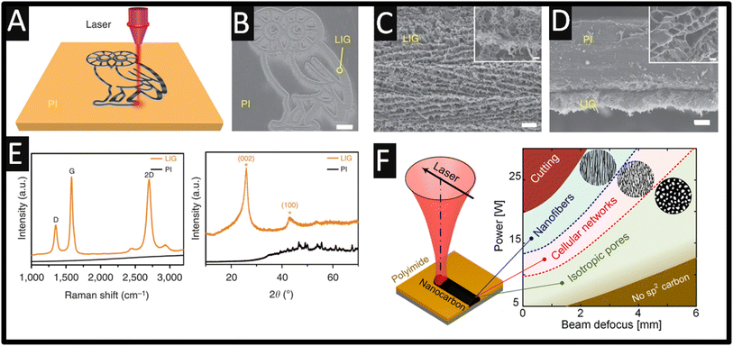 | ||
| Fig. 1 (A) Schematic of the synthesis process of laser-induced graphene from polyimide. (B) SEM image of laser-induced graphene patterned into an owl shape; scale bar, 1 mm. The bright contrast corresponds to laser-induced graphene surrounded by the darker-coloured insulating polyimide substrates. (C) SEM image of the laser-induced graphene film circled in (B); scale bar, 10 μm. Inset shows the corresponding higher magnification SEM image; scale bar, 1 μm. (D) Cross-sectional SEM image of the laser-induced graphene film on the polyimide substrate; scale bar, 20 μm. Inset shows the SEM image showing the porous morphology of laser-induced graphene; scale bar, 1 μm. (E) Representative Raman spectrum of a laser-induced graphene film and the starting polyimide film and XRD pattern of powdered laser-induced graphene scraped from the polyimide film. Figure reproduced from ref. 6. Copyright 2014 Nature. (F) Morphology diagram mapping the ranges of laser parameters (power and degree of beam defocusing) for creating different types of LINC (isotropic porous morphology, anisotropic cellular networks, and aligned woolly nanofibers) for a CW CO2 laser (wavelength λ = 10.5 mm) scanning at v = 500 mm s−1. Figure reproduced from ref. 7. Copyright 2021 American Chemical Society. | ||
Abdulhafez and co-workers7 studied morphological transitions in laser-induced graphene on polyimide substrates, where they explored the power as a function of the beam defocus. As shown in Fig. 1F, a useful zone diagram is presented which shows the morphology which ranges from various fluence values (F) corresponding to cutting (F = 25 J cm−2), nanofibers (F = 17 J cm−2), anisotropic cellular networks (F = 12 J cm−2) and isotropic pores (F = 5 J cm−2). The physicochemical characterisation of laser-induced graphene is dependent upon the material/substrate, laser type and associated parameters, e.g., wavelength, power and scanning speed, and environmental conditions also affect the hydrophilicity/hydrophobicity, nano- and micro-scale morphology, i.e., crystallinity, porosity, and chemical composition of the graphene produced.9,10 For example, various materials have been used to produce laser-induced graphene, which can be classed into thermoplastics (polyimide, poly(vinyl chloride) and polyphenylene sulfide), thermoset materials (polystyrene and phenolic resin), natural polymer materials (lignin and cellulose) and non-polymeric materials (charcoal and activated carbon).9,12 Furthermore, as shown in Fig. 2A, laser-induced graphene can be extended to bread, wood, cotton paper, cardboard and muslin cloth, which allows the approach to be utilised on biodegradable substrates through tuning the lasing parameters,12 noting that this is the Rice University (USA) Owl Mascot. That approach has used a CO2 laser with a wavelength of 10.6 μm, but this can be achieved on various substrates/surfaces using continuous wave, pulsed and ultrashort pulse lasers, as well as visible and infrared laser sources, where the power source and raw materials for the generation of different laser-induced graphene outputs have distinct advantages to form graphene.15
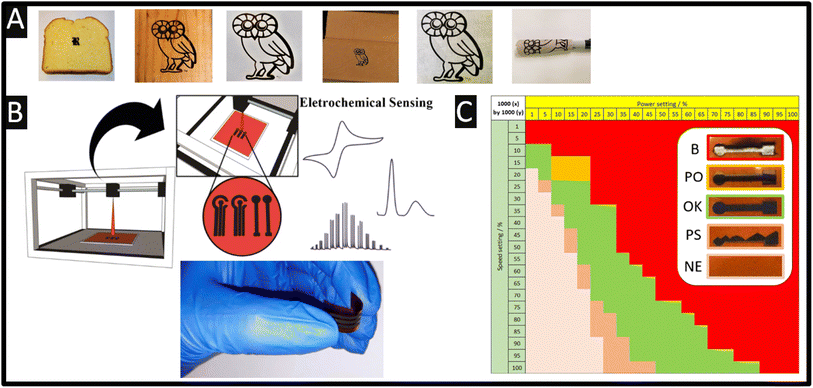 | ||
| Fig. 2 (A) Laser-induced graphene on (left to right) bread, fire-retardant treated pine wood, cotton paper, cardboard, grey muslin cloth and a muslin cloth wrapped around a marker pen. All owls depicted are 60 mm in height. Figure reproduced from ref. 12. Copyright 2018 American Chemical Society. (B) Illustration of the visible laser-printer machine showing the production of laser-induced graphene where a three-electrode configuration (1.5 cm × 4 cm) and single working electrode (1 cm × 4 cm) are shown. Also shown is the flexibility of laser-induced graphene electrodes. Figure reproduced from ref. 13 Copyright 2022 Springer. (C) Heatmap of the electrode outcome vs. power and speed settings at a pulse density of 1000 × 1000 (x by y) (colour code as indicated in the inset: green = ok, darker brown = partial scribing (PS), lighter brown = no effect (NE), orange = laser-induced graphene peeled off from the substrate (PO), and red = laser burned through the substrate (B)). Figure reproduced from ref. 14. Copyright 2021 Springer. Creative Commons Attribution 4.0 International License. | ||
One particular use of laser-induced graphene is within the realm of electrochemistry, where these materials have found application in batteries, water splitting devices, health and gas monitoring, fuel cells, and supercapacitors and are applied in various wearable and telemedicine platforms.12,16–20 In this mini-review, we introduce laser-induced graphene focusing on electrochemical-based sensors which can provide on-site analysis with a highly selective and sensitive output, whilst remaining cost-effective. We therefore summarise the use of laser-induced graphene as the basis of electroanalytical sensors and compare these critically against screen-printed and additive manufactured electrodes.
Laser-induced graphene electrodes
Laser-induced graphene electrodes have been utilised as the basis of sensors due to their rapid and easy approach of fabrication, high conductivity, flexibility, and unique micro- and macro-features. Most importantly, the fact that these are multi-layer graphene, it is the presence of edge plane sites/defects which has been extensively shown to be the origin of fast electron transfer.21,22 Another benefit is that production of laser-induced graphene does not need a template, as is the case when using screen-printed electrodes where a stencil design is required. For example, Fig. 2B shows the use of a visible laser-printer machine and the production of laser-induced graphene, where a three-electrode configuration (1.5 cm × 4 cm) and single working electrode (1 cm × 4 cm) can be realised. The real images of the produced laser-induced graphene electrode which highlights their flexibility are also shown.13 A useful approach has been reported by Clark and co-workers where the use of a stencil allowed minimal achievable resolution of the laser-induced graphene from 120 μm to 45 μm allowing a microarray electrode to be realised.23As mentioned above, laser-induced graphene can show variability between different research groups and batch-to-batch variations,24 where the graphene is dependent upon the material/substrate, laser type and associated parameters, e.g., wavelength, power and speed, and also environmental conditions. In each case, where researchers are producing laser-induced graphene, they need to physicochemically characterise their graphene using SEM, Raman, X-ray photoelectron spectroscopy (XPS) and electrochemistry. That said, this is often overlooked.
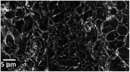
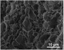
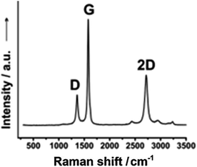
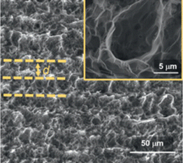
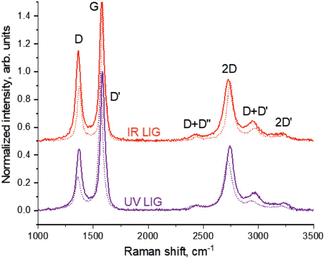
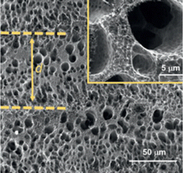
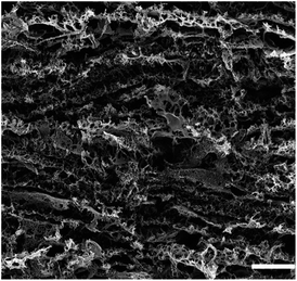
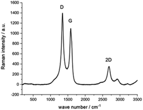
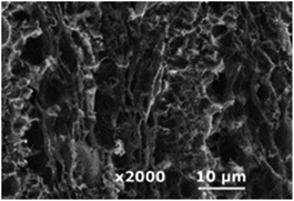
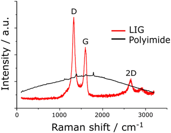
A useful approach has been reported by Behrent and co-workers14 who, as shown in Fig. 2C, have produced a heatmap of laser-induced graphene electrodes showing how power versus speed can either make a useful laser-induced graphene electrode, or not. They have identified these as follows: green is ok, darker brown is a result of partial scribing (see inset of Fig. 2C: PS), lighter brown indicates no effect (NE), orange resulting from laser-induced graphene which peeled off from the substrate (PO), while red is a result of the laser burning through the substrate (B); more authors need to follow the valuable approach by Behrent and co-workers.14 A useful review paper has been published by Muzyka and Xu25 which covers laser-induced graphene characterisation using Raman spectroscopy, sheet resistance, electrochemical active surface area, wettability (contract angles), and the heterogeneous electron transfer rate constant and compares different laser wavelengths with heterogeneous electron transfer rate constants, which can show great variations.25 We next summarise the physicochemical characterisation of their laser-induced graphene electrodes. In Table 1, one can see the different SEM images of laser-induced graphene electrochemical surfaces that are a result of different laser sources, where the Raman spectrum, the electrochemical area (Areal) and the heterogeneous rate constant (k0) reported for [Ru(NH3)6]3+/2+ and [Fe(CN)6]4−/3− redox probes are also shown. It is expected that the laser-induced graphene sensors will be dependent upon the surface and chemical morphology, indicating that researchers need to conduct physicochemical characterisation of their graphene surfaces.
| Fabrication approach | SEM | Raman spectra | A real | k 0/[Ru(NH3)6]3+/2+ | k 0/[Fe(CN)6]4−/3− | References |
|---|---|---|---|---|---|---|
| Visible-LIG (449 nm) |
|
|
0.20 cm2 | — | 0.0056 cm s−1 | 13 |
| IR CO2 laser (10.6 μm) |
|
|
1.3 cm2 | — | 0.0044 cm s−1 | 11 |
| IR CO2 laser (10.6 μm) |
|
|
— | 0.0231 cm s−1 | 0.282 cm s−1 | 26 |
| UV-LIG (355 nm) |
|
— | 0.00846 cm s−1 | 0.01 cm s−1 | 26 | |
| IR CO2 laser (10.6 μm) |
|
|
0.06 cm2 | — | 0.003 cm s−1 | 14 |
| IR CO2 laser (10.6 μm) |
|
|
0.092 cm2 | — | 0.0146 cm s−1 | 27 |
SEM (scanning electron microscopy)
SEM is critical to observe the structure of the formed laser-induced graphene structures, where one can see the micro and macro structures (see Table 1).Goniometry
Goniometry is used to determine the hydrophobicity, where solutions are carefully applied onto the laser-induced graphene surface where the average contact angle is reported. For example, an average contact angle using deionised water is reported to be 56° but it has been shown that the contact angle varied by more than 30% across four batch-to-batch variations.24Raman spectroscopy
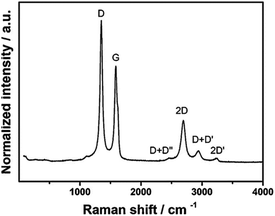
Raman spectroscopy is critical to identify the presence of micro and macro structures. As shown in Table 1, a typical Raman spectrum for laser-induced graphene is shown (first image) where the main peaks are identified, which are D, G and 2D bands and also D + D′′ and 2D′ bands. If we elaborate on this figure,13 we can observe the D (1343 cm−1), G (1591 cm−1), and 2D (2691 cm−1) vibrational bands. These arise from the Stokes phonon energy shift, where the G band is a primary in-plane vibrational mode, and the 2D band is a second-order overtone of a different in-plane vibration, the D band. Note that for graphene, one should only observe G and 2D bands, and the presence of the D band indicates defects. The G band represents the in-plane stretching vibrations of the sp2 bonded carbon atoms. Its position is affected by the number of layers present, where the peak shifts to lower wavenumbers as the number of graphene layers increases. The number of layers can be calculated from the peak position using the following equation where ωG is the band position, and n the number of layers present:28| ωG = 1581.6 + 11(1 + n1.6) | (1) |
Of further note is that the intensity of the G band decreases as the layers increase from mono- to tri-layer. The 2D band is also indicative of the number of layers present in the sample, which originates from a double resonance enhanced two-phonon lateral vibrational process. The 2D band changes in shape and position as the layers of graphene increase. The D-band is the peak which highlights defects within the sample, where the more intense this band is, the higher the level of disorder within the sample. This band is a result of ring breathing mode of sp2-carbon rings and must be adjacent to a defect to be Raman active. The D-band is a 1-phonon lattice vibrational process and is a double resonance band. The ratio of the intensities of I2D and IG bands, I2D/IG will be equal to 2 for high quality single layer graphene. The ratio changes to 1, 0.8 and 0.5 indicating that in each case, these correspond to double layer, few layer and multi-layer graphene. See ref. 29 for a calculator to help with the deduction of graphene layers. Lastly, one can observe a minor band D + D′ (2936 cm−1) which indicates the disorder structure of graphene with oxygen-containing groups where combined overtones of D + D′′ and 2D′ are also identified which indicate the formation of a graphite-like carbon structure.
XPS (X-ray photoelectron spectroscopy)
XPS can be used to analyse the elemental composition and chemical state of the material's surface. XPS can be used to measure the elemental composition and the chemical and electronic state of atoms. This approach is useful as it can be used to determine the carbon–oxygen content and identify them. Using a CO2 pulsed laser working at 10.6 μm using a scan speed of 160 mm s−1, manufacturing laser-induced graphene has shown, via XPS, an % atomic C of 76.6, % atomic O of 16.6, while % atomic nitrogen and silicon are 6 and 0.8 respectively, which are ascribed to C–O–C, C–N and C![[double bond, length as m-dash]](https://www.rsc.org/images/entities/char_e001.gif) O functional groups.30 The use of functional groups enhances surface wettability assisting with the adsorption and desorption of ions and enhancing interaction with the electrolyte. For example, it has been shown that oxygenated species decrease the electron transfer kinetics of ferrocyanide using basal plane and edge plane pyrolytic graphite electrodes.31 On the other hand, others report that oxygenation of the single-walled carbon nanotube ends is known to speed up the electron transfer kinetics32 – understanding which oxygenated species are present is critical and needs to be reported.
O functional groups.30 The use of functional groups enhances surface wettability assisting with the adsorption and desorption of ions and enhancing interaction with the electrolyte. For example, it has been shown that oxygenated species decrease the electron transfer kinetics of ferrocyanide using basal plane and edge plane pyrolytic graphite electrodes.31 On the other hand, others report that oxygenation of the single-walled carbon nanotube ends is known to speed up the electron transfer kinetics32 – understanding which oxygenated species are present is critical and needs to be reported.
Electrochemical characterisation
The heterogeneous electrochemical rate constant, k0, is calculated as an average from three sets (minimum) of scan rate studies for each electrode using an appropriate redox probe using the quasi-reversible electrochemical reactions through the following Nicholson formula:33| ψ = k0[πDnνF/(RT)]−1/2 | (2) |
| ψ = (−0.6288 + 0.0021X)/(1 − 0.017X) | (3) |
| k0 = 2.18[DαnνF/(RT)]1/2exp[−(α2nF/RT)ΔEp] | (4) |
 | (5) |
 | (6) |
| %Real = (Areal/Ageo) × 100) | (7) |
As can be seen in Table 1, there are many different micro and macro structures produced using different lasers forming laser-induced graphene, which are multi-layer graphene where the heterogeneous electrochemical rate constant and different electrochemical areas can vary. This indicates that laser-induced graphene electrodes are similar to solid carbon electrodes.39–41 As mentioned above, it has been shown that oxygenated species decrease the electron transfer kinetics of ferrocyanide using basal plane and edge plane pyrolytic graphite electrodes31 but others report that oxygenation of the single-walled carbon nanotube ends is known to speed up the electron transfer kinetics.32 One must understand the use of the redox probes in terms of their inner-sphere and outer-sphere nature. For example, it is known that [Ru(NH3)6]3+/2+ is a near-ideal outer-sphere redox probe, while [Fe(CN)6]4−/3− is known as an inner-sphere redox probe which is strongly influenced by the state of the electrode surface in terms of the surface chemistry, microstructure and oxygenated species. This may account for the fast heterogeneous electrochemical rate constant reported using laser-induced graphene, as shown Table 1. Ultimately, it is highly encouraged for researchers reporting the formation and use of laser-induced graphene to characterise and benchmark their material using the list of approaches highlighted above.
Laser-induced graphene sensors
Table 2 provides a snapshot of the use of laser-induced graphene electrochemical sensors, which it is shown in alphabetical order in terms of the analyte being measured alongside. These cases are reported together with the substrate graphene is formed on, the wavelength of the laser source and both the applied power and speed. Moreover, Table 2 summarises the use of laser-induced graphene towards various analytes along with their analytical performance (linear range and limit of detection (LoD)) and real sample application.| Analyte | Modification | Laser wavelength | Parameters (substrate/power/speed) | Linear range | Limit of detection | Sample medium | Comments | References |
|---|---|---|---|---|---|---|---|---|
| a Key: Ag NPs: silver nanoparticles; Au NPs: gold nanoparticles; DPPH: 2,2-diphenyl-2-picrylhydrazyl radical; GO: graphene oxide; HPLC: high performance liquid chromatography; Pd NPs: palladium nanoparticles; Pt-AuNPs: platinum-gold nanoparticles; PDMS: polydimethylsiloxane; NPs: nanoparticles; RGO: reduced graphene oxide; PVDF: polyvinylidene fluoride; EMImTFSI: 1-ethyl-3-methylimidazolium TFSI; GOx: glucose oxidase; PEDOT: poly(3,4-ethylene dioxythiophene); COOH-MWCNTs: carboxylated multi-walled carbon nanotubes; PVDF: polyvinylidene fluoride. | ||||||||
| Acetaminophen | RGO | 1064 nm | GO/30 W | 0.099–1978 μM | 5.2 nM | River, urine and tablet | — | 42 |
| 4-Aminophenol | MWCNTs-polyaniline | 405 nm | Kapton/2 W | 0.1–55 μM | 0.006 μM | Tap water and pharmaceutical | — | 43 |
| Aristolochic acid and roxarsone | MoS2/MXene | 10.6 μm | CO2 laser/PI/3.2 W/2.8 cm s−1 | 0.01–874 μM | 16.5 and 2.31 nM | Human blood serum | Simultaneous sensing | 44 |
| Ascorbic acid, dopamine and uric acid | — | 10.6 μm | PI/2.4–5.4 W/0.7–23 in s−1 | 10–680, 0.5–32.5, and 0.5–19.5 μM | 7.3, 0.27, and 0.22 μM | — | Simultaneous sensing | 45 |
| Ascorbic acid, dopamine and uric acid | Pt NPs | 10.6 μm | PI/2.4–5.4 W/0.7–23 in s−1 | 10–890, 0.5–56, and 1–63 μM | 6.1, 0.07, and 0.22 μM | — | Simultaneous sensing | 45 |
| Antioxidant capacity | — | 10.6 μm | CO2 laser PI/1.4 W/40 mm s−1 | 2–900 μM DPPH | 0.6 μM DPPH | Tea | Indirect analysis by DPPH detection | 46 |
| Atropine | — | 10.6 μm | CO2 laser PI/0.9 W/20 mm s−1 | 5–35 μM | 1 μM | Beverages (cola soft drink, energetic drink, beer, white wine, and whisky) | Electrode assembly within a 3D-printed cell | 47 |
| Carbendazim | Pt NPs | — | PI/1.38 W/4 cm s−1 | 1–40 μM | 0.67 μM | Wastewater | — | 48 |
| Chloramphenicol | — | 10.6 μm | CO2 laser PI/1.4 W/40 mm s−1 | 10–160 μM | 1.0 μM | Honey | — | 49 |
| Ciprofloxacin | — | 449 nm | PI/0.84 W/20 mm s−1 | 1–75 μM | 0.2 μM | Milk | Hypercube 3D printer with a visible laser source | 13 |
| cTn-I | ZnFe2O4 NPs/DNA aptamer | 10.6 μm | CO2 laser/PI/3.2 W/2.8 cm s−1 | 0.001–200 ng mL−1 | 0.001 ng mL−1 | Human serum | — | 50 |
| Dopamine | Pt-AuNPs/PDMS | — | CO2 laser. PI/7.6 W/200 mm s−1 | 5–30 μM | 75 nM | Human urine | — | 51 |
| Glucose | PEDOT/Au NPs/GOx | 450 nm | PI/5.5 W | 5 μM–2 mM | 2 μM | Artificial sweat and urine and fetal bovine serum | Nano Pro-III laser printer | 52 |
| Glucose | Chitosan/GOx | 450 nm | PI/7 W | 0–8 mM | 0.431 mM | — | Laser engraving machine | 53 |
| Glucose | GOx | 10.6 μm | CO2 laser/paper/5 W/127 cm s−1 | 1–15 mM | 0.13 mM | — | — | 54 |
| Glucose | Pt NPs GOx | 10.6 μm | PI/9.6 W/150 mm s−1 | 0.0003–2.1 mM | 300 nM | Sweat | — | 55 |
| Glucose | Cu NPs | 10.6 μm | CO2 laser/PI | 0.03–4.5 mM | 0.023 μM | Saliva | — | 56 |
| Glucose | Au NPs/Ni NPs | 10.6 μm | CO2 laser/PI | 0–30 mM | 1.5 μM | Sweat and cell culture media | — | 57 |
| Hydrogen peroxide | Ag NPs | — | Infra-red laser. 780 nm 5 mW | 10–10![[thin space (1/6-em)]](https://www.rsc.org/images/entities/char_2009.gif) 000 M 000 M |
7.9 M | Milk | — | 58 |
| Hydrogen peroxide | Prussian blue | 10.6 μm | CO2 laser PI/0.9 W/20 mm s−1 | 1–200 μM | 0.26 μM | Milk and mouthwash | Combination with batch-injection analysis | 59 |
| Ivermectin | — | 10.6 μm | CO2 laser PI/0.9 W/20 mm s−1 | 10–100 μM | 1.6 μM | Tap water, synthetic urine and tablets | — | 60 |
| Methane | Pd NPs/PVDF/EMImTFSI | — | CO2 laser. PI/10% power/25 mm s−1 | 10–50 ppm | 9.2 ppm | — | 61 | |
| m6A-RNA and 5mC-ssDNA | Au NPs | PI/power at 30%, speed at 20%, and a focus height of 25 mm | 0.01–10 nM | 2.81 and 9.53 pM | HeLa cells | Laser engraving | 62 | |
| Neonicotinoids (clothianidin, imidacloprid, thiamethoxam and dinotefuran) | — | 10.6 μm | PI/5.25 W/279 mm s−1 | 10–40 μM | 823, 384, 338, and 682 nM | River water | Simultaneous sensing | 63 |
| Nitrite | COOH-MWCNTs/Au NPs | 405 nm | Kapton/50 mm s−1 | 10–140 μM | 0.9 μM | Tap water | — | 64 |
| Picric acid | 10.6 μm | CO2 laser/cardboard/5 W/10 mm s−1 | 0.48–2.0 mM | — | — | Proof-of-concept | 65 | |
| Potassium and ammonium ions | Ionophore membrane | 10.6 μm | CO2 laser/PI/speed 7%/power 10%1 | 0.3 mM–150 mM | 100 and 30 μM | Human urine | 66 | |
| Uric acid and nitrite | — | 449 nm | PI/0.84 W/20 mm s−1 | 10–100 and 10–70 μM | 0.07 and 0.27 μM | — | Hypercube 3D printer with a visible laser source | 13 |
| Uric acid | — | 10.6 μm | CO2 laser/paper/850 W/30 mm s−1 | 10–250 μM | 3.97 μM | Human urine | — | 64 |
| Sulfamethoxazole | 2D hexagonal boron nitride | 450 nm | PI/5.2 W/0.5 cm s−1 | 0.5–362.5 μM | 0.11 μM | Milk and lake water | Compared with HPLC | 67 |
| Thrombin | 1-Pyrenebutyric acid/Aptamer | 10.6 μm | PI/0.81 W/5.8 cm s−1 | 1–100 pM | 1 pM buffer, 5 pM in serum | Fetal calf serum | X-660 laser cutter platform | 11 |
| Tyrosine | — | 10.6 μm | CO2 laser PI/0.9 W/20 mm s−1 | 5–30 μM | 1.5 μM | Artificial urine | — | 68 |
One can see that aristolochic acid and roxarsone have been simultaneously measured with a very low LoD of 16.5 and 2.31 nM.44 Aristolochic acid has been associated with urinary epithelial cancer, renal tumours, and renal failure related to the intake of herbal medicine derived from Aristolochia plants, while roxarsone is an organoarsenic chemical widely used in poultry farming which can be linked to toxic and carcinogenic effects in humans; therefore, there is a need for an electrochemical sensor for monitoring both compounds.44
An innovative approach for the measurement of methane has been reported using laser-induced graphene substrates.61 Using an interdigitated laser-induced graphene design, palladium nanoparticles (50 nm) are decorated on porous polyvinylidene fluoride (PVDF) with 1-ethyl-3-methylimidazolium TFSI (EMImTFSI) in an N-methylpyrrolidone (NMP) layer and then painted onto the electrodes. The interdigitated laser-induced graphene design (see Fig. 3) is composed of 14 anode/cathode fingers, each with a dimension of 13 × 0.4 mm and a spacing of 0.5 mm between them. Also shown in Fig. 3B is the characterisation of laser-induced graphene electrodes with the Raman spectrum of the laser-induced graphene electrode material, which reports multi-layer graphene. Also shown is a schematic (Fig. 3B) of the dimensions of the laser-induced graphene electrodes and an indication of where the electrolyte is applied. A cross-section SEM image of two adjacent electrodes shows that the electrode structure is not completely embedded within the polyimide, but the porous laser-induced graphene electrodes are ∼100 μm above the plane of the unexposed polyimide film. The sensor is applied to the measurement of methane, where the electrochemical procedure transforms methane into carbon dioxide and water. The author reports that this sensor gives a linear range of 10–50 ppm and a LoD of 9.2 ppm, which is 4 orders of magnitude lower than other electrode designs.61
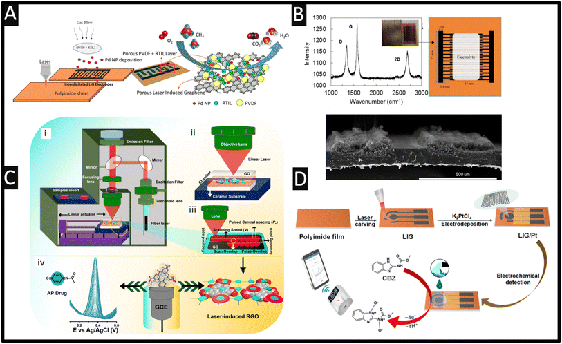 | ||
| Fig. 3 (A) Schematic of the fabrication process of the electrochemical methane sensor. A CO2 laser is used to convert the polyimide sheet into a patterned, interdigitated laser-induced graphene design. Palladium nanoparticles are decorated where porous polyvinylidene fluoride (PVDF) with 1-ethyl-3-methylimidazolium TFSI (EMImTFSI) in an N-methylpyrrolidone (NMP) layer is painted onto the electrodes. (B) Characterisation of laser-induced graphene electrodes with Raman spectra of the laser-induced graphene electrode material, photograph of electrodes prior to applying the electrolyte, a sketch of the interdigitated electrodes with dimensions and a SEM image of the cross section of the laser-induced graphene electrodes. Figures reproduced from reference 61. Copyright 2018 American Chemical Society. (C) Schematic setup of the fibre laser system (i), zoomed-in schematic showing the scanning of the laser (ii), laser scanning path (iii) and the electrochemical detection of the antipyretic (iv). Figure reproduced from reference 42. Copyright 2024 Royal Society of Chemistry. (D) A summary of a platinum modified laser-induced graphene electrochemical sensor and its application for the real-time detection of carbendazim in wastewater samples. Figure reproduced from ref. 48. Open Access. | ||
Fig. 3C shows the experimental set-up for the laser-induced technique used in the fabrication of reduced graphene oxide.42 A graphene oxide solution is coated onto an alumina ceramic (Al2O3) substrate through drop coating. It is placed in an oven for 2 h at 60 °C, after which, a 1064 nm laser is used with fibre optics via a telecentric lens (specification: f = 125 mm, λ = 1064 nm). The laser is passed over an excitation filter and reflected by a shrinking mirror into a mirror spot and focused by using an objective lens to excite graphene on the ceramic substrate.42 The ceramic plate was placed on a sample holder and fixed with a linear actuator, where the substrate was scanned by moving the stage in the xy-direction.42 In essence, the use of the laser forms reduced graphene oxide when used within an open atmosphere. This is confirmed via XRD, Raman spectroscopy and XPS. To show the use of laser-induced reduced graphene oxide, the authors explore the sensing of acetaminophen, one of the most commonly used medications in the world, where they can measure over the range of 0.099–1978 μM, and a LoD of 5.2 nM is reported. They apply their sensor to the detection of acetaminophen in spiked river and urine samples, as well as within a pharmaceutical tablet; this approach provides a low-cost, environmentally friendly method, and offers large-scale manufacturing of reduced graphene oxide. In another example, the use of platinum decorated laser-induced graphene electrodes has been reported for the sensing of carbendazim.48 Carbendazim is a fungicide that is regulated in many countries and banned in others. As such, there is a need for the sensing of carbendazim to ensure that high levels are avoided, which can result in potential health risks and environmental contamination.69 The sensor developed for this application is shown in Fig. 3D, where a polyimide film is exposed to a laser and then modified using electrodeposition of platinum nanoparticles (70 nm diameter) onto the formed graphene. It shows a porous structure and has lattice defects as reported using SEM, Raman spectroscopy and XPS. This sensor was shown to be successful in the measurement of carbendazim with an LoD of 0.67 μM with a linear range of 1–40 μM, where good recoveries (88.89–99.50%) are shown in wastewater samples. In another study involving a facile approach to form laser-induced graphene electrodes, Kucherenko and co-workers used this as a solid-state ion-selective electrode for the simultaneous measurement of potassium and ammonium ions using an ionophore membrane.66 This sensor provided a linear range of 0.3–150 mM and LoD of 100 μM and 30 μM for potassium and ammonium ions respectively. The authors used their sensor for the measurement of potassium and ammonium ions in urine to help monitoring hydration levels in different patients.
Others have shown that laser-induced graphene can be realised using paper-based electroanalytical devices. As shown in Fig. 4A, one can see that they can readily produce laser-induced graphene upon paperboard.65 This approach allows the researchers to produce laser-induced graphene on paperboard using a CO2 laser, after which, they painted a reference electrode with conductive silver ink. This was used as a proof-of-concept approach, which they tested towards the sensing of picric acid. The electrochemical reduction of this compound provides three distinct reduction processes at −0.35, −0.47, and −0.62 V (vs. silver) corresponding to the electroreduction of the nitro groups of picric acid, where the reduction wave at the lowest potential (−0.15 V) corresponds to the formation of a radical anion species.65 This approach has been extended to develop a laser-induced graphene electrode for the sensing of uric acid, which gave a linear range of 10–250 μM with a LoD of 3.97 μM which was tested using spiked human urine.64 The use of laser-induced graphene electrodes has been also investigated for the measurement of nitrite, as shown in Fig. 4B.64 In this work, the use of a bare laser-induced graphene electrode has been initially explored using a redox probe of potassium ferricyanide/ferrocyanide with a reported electrochemical area of 7.62 mm2. The use of gold nanoparticles (12.9 nm diameter), MWCNTs and gold nanoparticles/COOH functionalised MWCNTs (drop cast) increase the electrochemical area to 9.27, 9.45 and 13.60 mm2, respectively. Furthermore, the authors report that the charge transfer resistance decreased from 2911 Ω using a bare laser-induced graphene electrode to 448 Ω with gold nanoparticles/COOH functionalised MWCNTs. These electrode configurations are explored toward the electrochemical oxidation of nitrite, where the bare induced graphene electrodes gave rise to a peak observed at +0.68 V which moved to +0.75 V using the gold nanoparticles/COOH functionalised MWCNTs, but results in a larger peak height which will provide a useful response for the sensing of nitrite. The COOH-MWCNTs/gold nanoparticle modified laser-induced graphene electrodes are shown to report a linear range of 10–140 μM towards nitrite and an LoD of 0.9 μM. They applied this to spiked tap water samples reporting recoveries of 91.5–96.1%, the mechanism of the electrochemical oxidation of nitrite is summarised in Fig. 4B.
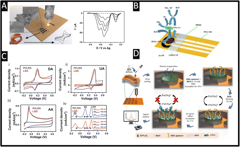 | ||
| Fig. 4 (A) The use of laser-induced graphene formed upon paperboard. Also shown are the differential pulse voltammograms obtained towards the measurement of picric acid in the presence of 0.48, 0.91, 1.30, and 2.0 mM. Figure reproduced from ref. 65. Copyright 2017 Wiley. (B) An image showing the proposed mechanism of the electro-oxidation of nitrite using a laser-induced graphene electrode modified with COOH-MWCNT and with gold nanoparticles (all drop cast). Figure reproduced from ref. 64. Copyright 2021. (C) Cyclic voltammograms of laser-induced graphene and platinum laser-induced graphene electrodes in a pH 7.0 buffer containing (i) 1 mM dopamine (DA), (ii) 1 mM uric acid (UA) and (iii) 1 mM ascorbic acid (AA). Scan rate: 50 mV s−1. Differential pulse voltammetry curve (iv) of laser-induced graphene and platinum laser-induced graphene electrodes, pH 7.0, containing 1 mM AA, 40 μM DA and 40 μM UA. All measurements were performed relative to an external Ag/AgCl (3 M KCl) reference electrode. Figure reproduced from ref. 45 Copyright 2016 Wiley. (D) Schematic illustration of the ZnFe2O4 modified laser-induced graphene cTn-I aptasensor. Fabrication of laser-induced graphene electrodes using the laser-scribing method and modification with ZnFe2O4 by drop-casting to prepare a laser-induced graphene/ZnFe2O4 electrode. A mixture of a thiol-modified DNA aptamer specific to cTn-I and mercaptohexanol (MCH) was immobilized on the electrode surface. MCH helps in the proper folding of the DNA aptamer. Incubation of BSA solution for 45 min to reduce non-specific adsorption. Different concentrations of cTn-I solution were incubated on the cTn-I aptasensor. The electrochemical signal was measured before and after the binding of cTn-I. Due to the attachment of cTn-I, the diffusion of the redox probe to the electrode surface was hindered, resulting in a decrease in the peak current values, directly correlated with the amount of cTn-I molecules attached to the aptasensor surface. Figure reproduced from ref. 50. Copyright 2021 Elsevier. | ||
Fig. 4C shows the use of laser-induced graphene and platinum nanoparticle laser-induced graphene electrodes in the presence of 1 mM dopamine (DA), 1 mM uric acid (UA) and 1 mM ascorbic acid (AA) recorded separately.45 Analysis by the authors showed that the electrochemical area corresponds to 9.177 mm2 for laser-induced graphene and in comparison a value of 10.383 mm2 is reported for the platinum nanoparticle laser-induced graphene electrodes, which increased the area by 13.14%.45 There is very little difference between the laser-induced graphene and platinum laser-induced graphene electrodes, which questions the need of carrying out such surface functionalisation with platinum. Interestingly, the separation between dopamine, uric acid and ascorbic acid is feasible where the peaks are well-resolved with and without Pt, as shown in Fig. 4C. This approach is summarised by the authors due to (i) rapid electron transport properties of a porous graphene network, (ii) rich in edge plane like sites/defects, which can provide catalytic activity, and (iii) the 3D hierarchical and porous network providing enough accessibility to biomolecules.45
Another notable study is reported by Zeng and co-workers67 who produced a laser-induced graphene surface modified with 2D-hexagonal boron nitride via drop-casting. This sensor has been used in the measurement of sulfamethoxazole, which occurs via an electrochemical oxidation mechanism and undergoes one electron and one proton loss, giving a linear range of 0.5–362.5 μM and an LoD of 0.11 μM. The repeatability has been explored using 20 successive measurements, and the RSD was found to be 4.01%. In terms of the number of electrodes, the authors explored 10 different electrodes, which gave a relative standard deviation (RSD) of 4.65%. The selectivity towards the measurement of sulfamethoxazole is explored where they added in NaCl, KCl, MgCl2, and CaCl2 at 100-fold excess concentration and glucose with 10-fold excess concentration to 50 μM sulfamethoxazole. Also, they studied glutamic acid, arginine, and hypoxanthine with 1-fold excess concentration. All these compounds did not affect the measurement of sulfamethoxazole with RSD values less than 5%. This sensor was shown to be successful in the measurement of lake water and milk samples. In this work, while water samples collected from Jiangxi Agricultural University were processed using a 0.22 μm filter to remove the suspended particles, the commercial milk underwent an extraction procedure in a buffer/acetonitrile 50% (v/v) solution before analysis. Subsequent samples spiked with 27 and 55 μM sulfamethoxazole were analysed by HPLC and electrochemistry. Both produced recoveries in the range of 97.5–108.2%, with RSD values below 5% which showed there was no significant difference between the two methods, which also suggests a promising practical application in spiked sample analyses of the sensor.67 It is important to highlight that validation of electrochemical sensors using laboratory-based instrumentation is of critical importance when such sensing devices are applied for real sample analysis.
Laser-induced graphene biosensors
Laser-induced graphene biosensors have been extensively reported, where the laser-induced graphene does not contribute to the sensing of the biomolecules under investigation but instead supports the use of nanoparticles which can increase active sites, enhance the number of immobilised biomolecules, and improve the electroanalytical response of the sensor. For example, a laser-induced graphene surface has been utilised as the basis of an aptasensor directed toward the sensing of cardiac troponin-I (cTn-I) proteins that are a clinically validated biomarker for the detection of acute myocardial infarction – as shown in Fig. 4D which shows how they fabricated the sensor.50 In this approach, ZnFe2O4 is synthesised using a wet chemical methodology and drop cast onto the laser-induced graphene surface which is allowed to dry. Next, DNA aptamer (thiol modified Anti-cTn-I: CGTGCAGTACGCCAACCT TTCTCATGCG CTGCCCCTCTTA) and mercaptohexanol are incubated for 16 h, after which bovine serum albumin is applied for 45 min to reduce non-specific adsorption. This approach uses the redox probe potassium ferricyanide/ferrocyanide, where the cTN-I binds with the surface DNA aptamer and blocks the surface sites causing the signal to decrease. A linear range of 0.001–200 ng mL−1 and an LoD of 0.001 ng mL−1 are shown to be feasible. Note that cTn-I levels below 0.6 ng mL−1 present in serum are considered normal, while 0.7–1.4 ng mL−1 suggest a minor myocardial injury and over 1.5 ng mL−1 indicate myocardial necrotic damage suggesting that this sensor can discriminate between a normal situation and myocardial necrotic damage. This sensor was explored in the presence of potential interference from cholesterol, glucose, myoglobin, cTn-T, and cTn-C and compared to the response for cTn-I. The sensor was explored toward 8.8, 8.2, 7.3, 6.5 and 5.9 fold excess for the same concentration (50 ng mL−1) of each analyte, respectively.50 The only interferents were cTn-C and cTn-T, which showed more adsorption onto the sensors, but the authors assure us that their sensor is highly selective for the measurement of cTn-I; potentially a change in blocking solution would benefit this work. This sensor was shown to be used for the measurement of cTn-I in spiked human serum using different amounts of cTn-1 of 0.001, 0.01, 0.1, 1, 10 and 100 ng mL−1. The authors concluded that the performance of their sensor is a result of the use of ZnFe2O4 increasing the electroactive surface area and electrocatalytic activity where the laser-induced graphene electrode surface acts as “electrically wiring”, where presumably other electrodes could be used; as shown by the authors50 there are more sensitive approaches with very low linear ranges ∼pg mL−1 levels using other carbon substrates (e.g., screen-printed carbon electrodes).70Other approaches have developed biosensors for the measurement of glucose using laser-induced graphene electrodes, as shown Table 2. There is still an obvious need for the measurement of glucose that can provide rapid, on-the-spot readings within human blood. The concentration of glucose needs to be in the normal human body range, where a reduction and excess can lead to hypoglycemia and hyperglycemia, respectively. For example, a linear range of 5 μM–2 mM and an LoD of 2 μM using poly(3,4-ethylene dioxythiophene) (PEDOT) and gold nanoparticles (20 nm diameter) with glucose oxidase upon a laser-induced graphene electrode have been reported.52 As shown in Fig. 5A, 3,4-ethylene dioxythiophene (EDOT) monomers are electrochemically polymerized on the laser-induced graphene electrode surface to form a PEDOT film. Next, gold nanoparticles are electrochemically deposited on the laser-induced graphene electrode surface by potentiostatic deposition.52 This is then modified with 11-mercaptoundecanoic acid (MUA) onto which a mixed solution of glucose oxidase (GOx) and glutaraldehyde (GA) is drop cast. Using the Randles–Ševčík equation they deduced the effective electrochemical area to be 4 times greater than the geometric area, which gave rise to the performance of the sensors. This sensor was used to sense glucose in artificial urine, fetal bovine serum and artificial sweat, where the recoveries of glucose with different concentrations are 61.34–111.93%, 81.72–159.66% and 72.68–125.00% respectively.52 Non-enzymatic glucose-based laser-induced graphene sensors outperform enzymatic ones when one considers the cost, sensitivity, stability, and of course, operating duration. To this end, laser-induced graphene modified with copper nanoparticles gives rise to the measurement of glucose reporting a sensitivity of 2665 μA mM−1 cm−2, a limit of detection of 0.023 μM and a linear range of 0.03–4.5 mM.56 Another notable study reported laser-induced porous graphene which has been fabricated and decorated with nickel and gold nanoparticles towards the sensing of glucose, reporting a high sensitivity of 3500 μA mM−1 cm−2, a linear range of 0–30 mM, a LoD of 1.5 μM and a response time of less than one second.57 Interestingly, the authors applied their sensor to the measurement of glucose through sweat providing a flexible sensor attached to the arms of a human subject. The authors consider the response of sensing in a flat or bending state reporting excellent mechanical durability using up to 500 cycles of bending and electrochemical stability through immersion in phosphate buffer solution for up to 30 days. Using a commercial sensor, they validated their laser-induced graphene-based sensor within sweat, demonstrating that their non-enzymatic laser-induced graphene glucose sensor could also be integrated with wireless measurement units to provide real-time monitoring capabilities.57
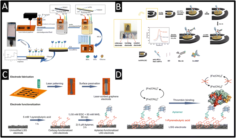 | ||
| Fig. 5 (A) An overview of the glucose sensing analysis. Figure reproduced from ref. 52. Copyright 2024 Royal Society of Chemistry. (B) Schematic illustration of the biosensor modification process showing how the sensor works. Figure reproduced from ref. 62. Copyright 2024 Royal Society of Chemistry. (C) Electrode fabrication and functionalization process. (D) Schematic of the electrochemical thrombin detection mechanism with increasing concentrations of thrombin, and the diffusion of the redox marker hexacyanoferrate(III) to the electrode surface is hampered. This results in a decrease in the peak currents obtained from voltammetric measurements. Figures reproduced from ref. 11. Copyright 2017 American Chemical Society. | ||
The use of laser-induced graphene biosensors has also been reported for the detection of methylation in DNA and RNA which is essential for the diagnosis and treatment of a wide range of diseases.62 As shown in Fig. 5B, a biosensor for the measurement of N6-methyladenosine (m6A-RNA) and 5-methylcytosine-single strand DNA (5mC-ssDNA) is designed and implement in HeLa cells. This approach utilised electrochemically deposited gold nanoparticles, sulfhydryl-modified nucleic acid chains, biotin-modified antibodies, and streptavidin-modified horseradish peroxidase (SA-HRP), where the peak current/signal is proportional to the concentration of m6A-RNA and 5mC-ssDNA in the hydrogen peroxide–hydroquinone (H2O2–HQ) system. This sensor allowed the measurement across the linear range of 0.01–10 nM with an LoD of 2.81 pM for m6A-RNA and 9.53 pM for 5mC-ssDNA. It is reported by the authors that the method utilises gold–sulfur bonding to immobilise the detection target, which improves the conductivity of the laser-induced graphene electrode and introduces an amplified portion of the signal by taking advantage of antigen–antibody specific binding.62 The stability of the biosensor was explored when they stored their sensor in a refrigerator (4 °C) for 0, 3 and 5 days and showed that the %RSD decreased by 9.42 for the 5-day detection, suggesting that the biosensor should not be stored for more than 5 days. This sensor was evaluated for the measurement of m6A-RNA and 5mC-ssDNA within spiked HeLa cells where they report recoveries of 105.4–111.0% and 95.3–98.8% respectively with a low %RSD of 0.8–1.3% and 0.7–1.3% respectively. This approach has potential to be explored further for point-of-care techniques for nucleic acid methylation detection in clinical applications.62
An outstanding approach using laser-induced graphene electrodes involves the use of an X-660 laser cutter platform with a wavelength of 10.6 μm – see Fig. 5C.11 These electrodes are modified with 1-pyrenebutyric acid for 1 h, which forms via π–stacking interactions. This then provides COOH-groups upon the electrode surface which allows covalent coupling using EDC/NHS with the antithrombin aptamer (5′-H2N-C6-GGTTGGTGTGGTTGG-3′) – see Fig. 5D. This sensor is used for thrombin detection, where increasing concentrations of thrombin stop the diffusion of the redox marker potassium hexacyanoferrate(III) to the electrode surface and produce a decrease in the peak currents. This sensor is shown to report a linear range of 1–100 pM with a low LoD of 1 pM in buffer and 5 pM in fetal calf serum. The sensor has a reported incubation time of 30 min which is shorter than others reported and the LoD compares favourably.11
Comparison of laser-induced graphene electrodes with screen-printed and additive manufactured electrodes
Screen-printed electrodes are a consolidated technology applied to the development of electrochemical sensors while additive manufacturing has emerged in the last ten years as a potential technology for the same purpose with additional advantages, which is also valid for laser-induced graphene electrodes. Table 3 summaries the advantages and disadvantages of laser-induced graphene electrodes in comparison to screen-printed electrodes39,71 and additive manufactured electrodes.72,73 We take every point in turn, and we comment upon each approach summarising the advantages and disadvantages of laser-induced graphene, screen-printed and additive manufactured electrodes.| Laser-induced graphene electrodes | Additive manufactured electrodes | Screen-printed electrodes | |
|---|---|---|---|
| Advantages | • Economical | • Economical | • Economical |
| • No need for screens to define the working electrode and associated electrodes | • No need for screens to define the working electrode and associated electrodes | • Flexible/bendable electrodes | |
| • Flexible/bendable electrodes | • Can provide flexible/bendable electrodes based on the filament that is used | • Bulk modified | |
| • Control of surface morphology | • 3D electrodes can be easily realised | • Abundant edge plane sites/defects | |
| • Abundant edge plane sites/defects | • Bulk modified | • Multiple sensing | |
| • Multiple sensing | • Control of surface morphology | • Different electrodes surface can be easily made (gold, silver, CNTs etc) | |
| • Highly reproducible | • Abundant edge plane sites/defects | • Comparable to gold standard laboratory approaches | |
| • Comparable to gold standard laboratory approaches | • Multiple sensing | • Portable | |
| • Portable | • Different electrodes surface can be easily made (e.g., bulk modified metal nanoparticles) | • Comparable to solid carbon electrodes | |
| • Comparable to solid carbon electrodes | • Comparable to gold standard laboratory approaches | • Commercially available inks (standardisation is feasible) | |
| • They are generally fabricated under ambient conditions; however, the inner gas environment can generate new morphologies and insert functional groups | • Portable | ||
| • Comparable to solid carbon electrodes | |||
| Disadvantages | • It cannot be bulk modified, so it needs surface-modification with nanoparticles, electrocatalysts/mediators, metallic films (e.g., gold, mercury, and bismuth), which can potentially limit their use | • Filaments need to be made to optimise for every application | • Screens are needed and need to be maintained |
| • Difficult standardisation across groups/methods and batch-to-batch variation and power, speed and beam defocus need to be adjusted and depend on the laser source | • 3D printer parameters need to be evaluated for every filament | • Longer time for preparation due to ink curing time; every different material needs to be cured separately (e.g., silver, carbon and insulating inks) | |
| • Conductive graphene tracks are easily removed by mechanical contact (electric contact requires extra attention) | • In some cases, electrochemical surface activation is required |
Laser-induced graphene, additive manufactured and screen-printed electrodes are shown to be economical, reproducible, comparable to those obtained by standard laboratory approaches, and allow one to control the surface morphology. They are easy to combine with portable electroanalytical setups, and therefore allow one to transfer the laboratory approach into the field. They all have abundant edge plane sites/defects, which promote fast electron transfer and results in sensitive electroanalytical approaches. Furthermore, they can all be fabricated onto flexible materials and they are all electrochemically comparable to solid carbon electrodes. Additionally, new designs, such as microbands, microdiscs, microdisc arrays, etc. using a stencil can be manufactured and also they can be used for multi-analyte sensing. One downside of laser-induced electrodes is that these need to be modified with gold nanoparticles, and with electrocatalysts/mediators as a post-processing approach, which may limit their use, such as on using electrochemical deposition. In comparison, bulk modified additive manufactured and screen-printed electrodes can be readily produced where screen-printed inks are modified with the desired micro/nanomaterial (e.g., macro/nanosized silver, gold, palladium, CNTs, graphene) which reduces the resistance between the material and the electrode surface and improves electron transfer properties.39 Such an approach provides a simple but effective strategy allowing one to create mass-produced electrochemical platforms.39 Furthermore, screen-printed metallic electrodes can be realised through changing the ink, and one can readily manufacture different electrode types, for example silver, gold, palladium, etc. The downside with screen-printed electrodes is that one needs to design and use a screen which needs to be maintained,39 while in the case of laser-induced graphene and additive manufactured electrodes, one does not need a screen. One aspect that also limits the use of additive manufactured electrodes, is that in some cases, electrochemical surface activation is required. Lastly, in all cases, these electrode configurations are comparable to solid carbon electrodes (∼10−3 cm s−1) where the k0 compares well, suggesting that these fabrication approaches should be routinely used for sensing.
Conclusions
We have overviewed the use of laser-induced graphene electrodes as the basis of sensors and we can summarise as follows:(1) The rapid and easy fabrication of laser-induced graphene sensors is an interesting approach for use as the basis of electroanalytical sensors. The electrodes are highly conductive, flexible, cost-effective, and have unique micro- and macro-features and eco-friendly production and the manufacturing of laser-induced graphene typically uses fewer chemicals and produces less waste than traditional graphene fabrication methods, making laser-induced graphene sensors more environmentally friendly, aligning well with sustainable manufacturing goals. Most importantly, these are multi-layer graphene, which contain using C–O/C![[double bond, length as m-dash]](https://www.rsc.org/images/entities/char_e001.gif) O etc. functional groups where edge plane sites/defects are favourable for electroanalysis.
O etc. functional groups where edge plane sites/defects are favourable for electroanalysis.
(2) As shown throughout, there are many types of laser-induced graphene and there can be variability between different research groups and batch-to-batch variations.24 The graphene is dependent upon the material/substrate, laser type and associated parameters and in future manufacturing laser maintenance, operational frequency and batch size should be considered.24 In each case, these need to be physicochemically characterised using SEM, Raman spectroscopy, XPS and electrochemistry, helping to benchmark the performance of the laser-induced graphene electrodes. Another area is to vary the length of the electrical connection of laser-induced graphene electrodes, which has shown that a shorter connection give rise to improvement in the electrochemical response using screen-printed electrodes.40
(3) The use of laser-induced graphene sensors is comparable with that of screen-printed and additive manufactured electrodes, but they have advantages and disadvantages which need to be considered – see Table 3 (e.g., they cannot be bulk modified with catalysts). Laser-induced formation of catalyst-modified graphene occurs through a single laser step; metal nanostructures have been incorporated as a post-treatment protocol by different strategies and steps to improve sensing properties of laser-induced graphene, which increases the time of preparation and decreases reproducibility.
(4) The use of laser-induced graphene sensors has been explored toward a range of useful analytes, but many do not validate their sensors with laboratory-based instrumentation which stops uptake and commercialisation.
(5) One needs to consider how do the different laser-induced graphene sensors compare with each other and how to choose the appropriate ones for a specific target application? The answer lies in the fabrication of laser-induced graphene sensors which is varied, providing different electrochemical based responses (see Table 1) where researchers need to physicochemically characterise and decide whether their sensor is useful for direct electron transfer processes, or they need to modify the surface using catalytic nanoparticles and enzymes/proteins, for instance.
Laser-induced graphene sensors have an optimistic future where researchers need to develop their sensors further exploring more challenging analytes in difficult media, e.g., real blood, saliva, sewage, etc. New strategies to incorporate different metal-based catalysts within graphene through a single laser irradiation procedure (one-step laser protocol) may enable the formation of next generation electrochemical laser-induced sensing materials with improved selectivity and sensitivity. Polyimide has been the main substrate used to generate laser-induced graphene sensors; however, other substrates can be investigated and paper is likely a promising material considering the generation of sustainable electrochemical sensors. On the other hand, paper as a substrate for laser-induced graphene sensors brings additional challenges to be overcome, aiming at high-performance benchmarked sensors. Lastly, the use of integration of laser-induced graphene sensors with internet of things (IoT) extends their use in smart infrastructure for real-time data gathering and responsive systems. Overall, we can state that laser-induced graphene sensors are likely to become increasingly versatile and accessible, supporting innovative solutions across health, environmental monitoring and smart infrastructure, to name just a few.
Data availability
No new data were generated or analysed as part of this review.Conflicts of interest
The authors declare no competing interests.Acknowledgements
RAAM is grateful to Conselho Nacional de Desenvolvimento Científico e Tecnológico (CNPq) for his fellowship (315838/2021-3).References
- A. R. Urade, I. Lahiri and K. S. Suresh, JOM, 2023, 75, 614–630 CrossRef PubMed
.
- E. Bernalte, R. D. Crapnell, O. M. Messai and C. E. Banks, ChemElectroChem, 2024, 11, e202300576 CrossRef
.
- N. Sharma, R. Dev Gupta, R. Chandmal Sharma, S. Dayal and A. Singh Yadav, Mater. Today: Proc., 2021, 47, 2752–2755 Search PubMed
.
-
R. Ramesh, in Graphene Production and Application, eds A. Sadia, M. S. Akhtar and S. Hyung-Shik, IntechOpen, Rijeka, 2020, Ch. 2, DOI:10.5772/intechopen.92258
.
- J. Phiri, P. Gane and T. C. Maloney, Mater. Sci. Eng., B, 2017, 215, 9–28 Search PubMed
.
- J. Lin, Z. Peng, Y. Liu, F. Ruiz-Zepeda, R. Ye, E. L. G. Samuel, M. J. Yacaman, B. I. Yakobson and J. M. Tour, Nat. Commun., 2014, 5, 5714 CrossRef PubMed
.
- M. Abdulhafez, G. N. Tomaraei and M. Bedewy, ACS Appl. Nano Mater., 2021, 4, 2973–2986 CrossRef
.
- A. C. Ferrari, J. C. Meyer, V. Scardaci, C. Casiraghi, M. Lazzeri, F. Mauri, S. Piscanec, D. Jiang, K. S. Novoselov, S. Roth and A. K. Geim, Phys. Rev. Lett., 2006, 97, 187401 CrossRef PubMed
.
- K. Avinash and F. Patolsky, Mater. Today, 2023, 70, 104–136 CrossRef
.
- N. Dixit and S. P. Singh, ACS Omega, 2022, 7, 5112–5130 CrossRef PubMed
.
- C. Fenzl, P. Nayak, T. Hirsch, O. S. Wolfbeis, H. N. Alshareef and A. J. Baeumner, ACS Sens., 2017, 2, 616–620 CrossRef PubMed
.
- Y. Chyan, R. Ye, Y. Li, S. P. Singh, C. J. Arnusch and J. M. Tour, ACS Nano, 2018, 12, 2176–2183 CrossRef PubMed
.
- W. R. P. Costa, R. G. Rocha, L. V. de Faria, T. A. Matias, D. L. O. Ramos, A. G. C. Dias, G. L. Fernandes, E. M. Richter and R. A. A. Muñoz, Microchim. Acta, 2022, 189, 185 CrossRef PubMed
.
- A. Behrent, C. Griesche, P. Sippel and A. J. Baeumner, Microchim. Acta, 2021, 188, 159 CrossRef PubMed
.
- F. Wang, K. Wang, B. Zheng, X. Dong, X. Mei, J. Lv, W. Duan and W. Wang, Mater. Technol., 2018, 33, 340–356 CrossRef
.
- H. Xiao, Y. Li, R. Chen, T. Xie, P. Xu, H. Zhu, J. He, W. Zheng and S. Huang, eScience, 2023, 3, 100134 CrossRef
.
- J. Zhang, C. Zhang, J. Sha, H. Fei, Y. Li and J. M. Tour, ACS Appl. Mater. Interfaces, 2017, 9, 26840–26847 CrossRef PubMed
.
- A. Kothuru and S. Goel, IEEE Trans. Electron Devices, 2022, 69, 1333–1340 Search PubMed
.
- M. Wang, Y. Yang and W. Gao, Trends Chem., 2021, 3, 969–981 CrossRef
.
- Y. Huang, R. Yang and M. G. Li, Adv. Funct. Mater., 2024, 34, 2407503 CrossRef
.
- T. J. Davies, C. E. Banks and R. G. Compton, J.
Solid State Electrochem., 2005, 9, 797–808 CrossRef
.
- D. A. C. Brownson, D. K. Kampouris and C. E. Banks, Chem. Soc. Rev., 2012, 41, 6944–6976 RSC
.
- K. M. Clark, D. T. Nekoba, K. L. Viernes, J. Zhou and T. R. Ray, Biosens. Bioelectron., 2024, 264, 116649 CrossRef PubMed
.
- Y. Tang, G. A. Moreira, D. Vanegas, S. P. A. Datta and E. S. McLamore, Micromachines, 2024, 15, 874 CrossRef
.
- K. Muzyka and G. Xu, Electroanalysis, 2022, 34, 574–589 CrossRef
.
- N. F. Santos, S. O. Pereira, A. Moreira, A. V. Girão, A. F. Carvalho, A. J. S. Fernandes and F. M. Costa, Adv. Mater. Technol., 2021, 6, 2100007 CrossRef
.
- R. R. A. Soares, R. G. Hjort, C. C. Pola, K. Parate, E. L. Reis, N. F. F. Soares, E. S. McLamore, J. C. Claussen and C. L. Gomes, ACS Sens., 2020, 5, 1900–1911 CrossRef
.
- H. Wang, Y. Wang, X. Cao, M. Feng and G. Lan, J. Raman Spectrosc., 2009, 40, 1791–1796 CrossRef
.
- Graphene Number of Layers Calculator From ID/IG and I2D/IG Ratio via Raman Spectroscopy – InstaNANO, https://instanano.com/all/characterization/raman/graphene-layers/, accessed June 2 Search PubMed.
- A. Lamberti, F. Perrucci, M. Caprioli, M. Serrapede, M. Fontana, S. Bianco, S. Ferrero and E. Tresso, Nanotechnology, 2017, 28, 174002 CrossRef
.
- X. Ji, C. E. Banks, A. Crossley and R. G. Compton, ChemPhysChem, 2006, 7, 1337–1344 CrossRef PubMed
.
- A. Chou, T. Böcking, N. K. Singh and J. J. Gooding, Chem. Commun., 2005, 842–844, 10.1039/B415051A
.
- R. S. Nicholson, Anal. Chem., 1965, 37, 1351–1355 CrossRef
.
- I. Lavagnini, R. Antiochia and F. Magno, Electroanalysis, 2004, 16, 505–506 CrossRef
.
- R. J. Klingler and J. K. Kochi, J. Phys. Chem., 1981, 85, 1731–1741 CrossRef
.
- A. García-Miranda Ferrari, C. W. Foster, P. J. Kelly, D. A. C. Brownson and C. E. Banks, Biosensors, 2018, 8, 53 CrossRef
.
- J. E. Randles, Trans. Faraday Soc., 1948, 44, 327–338 RSC
.
- A. Ševčík, Collect. Czech. Chem. Commun., 1948, 13, 349–377 CrossRef
.
- R. D. Crapnell and C. E. Banks, ChemElectroChem, 2024, 11, e202400370 CrossRef
.
- M. J. Whittingham, N. J. Hurst, R. D. Crapnell, A. Garcia-Miranda Ferrari, E. Blanco, T. J. Davies and C. E. Banks, Anal. Chem., 2021, 93, 16481–16488 CrossRef PubMed
.
- H. M. A. Amin, Y. Uchida, E. Kätelhön and R. G. Compton, J. Electroanal. Chem., 2021, 880, 114891 CrossRef
.
- K.-Y. Hwa, R. Murugan, S.-F. Tseng, A. Santhan and J.-Y. Lin, Environ. Sci.: Nano, 2024, 11, 951–968 RSC
.
- S. Nasraoui, S. Ameur, A. Al-Hamry, M. Ben Ali and O. Kanoun, Sensors, 2022, 22, 833 CrossRef PubMed
.
- U. Rajaji, P.-S. Ganesh, S.-Y. Kim, M. Govindasamy, R. A. Alshgari and T.-Y. Liu, ACS Appl. Nano Mater., 2022, 5, 3252–3264 CrossRef
.
- P. Nayak, N. Kurra, C. Xia and H. N. Alshareef, Adv. Electron. Mater., 2016, 2, 1600185 CrossRef
.
- N. l. I. Inoque, D. A. Araújo, D. M. de Lima, R. M. F. Sousa, T. R. L. C. Paixão and R. A. Munoz, ACS Food Sci. Technol., 2024, 4(6), 1589 CrossRef CAS
.
- T. A. Matias, D. L. Ramos, L. V. Faria, A. de Siervo, E. M. Richter and R. A. Muñoz, Microchim. Acta, 2023, 190, 297 CrossRef CAS
.
- L. Wang, M. Li, B. Li, M. Wang, H. Zhao and F. Zhao, Foods, 2023, 12, 2277 CrossRef
.
- N. I. Inoque and R. A. A. Munoz, Anal. Methods, 2024, 16, 6793 RSC
.
- S. Rauf, V. Mani, A. A. Lahcen, S. Yuvaraja, T. Beduk and K. N. Salama, Electrochim. Acta, 2021, 386, 138489 CrossRef
.
- X. Hui, X. Xuan, J. Kim and J. Y. Park, Electrochim. Acta, 2019, 328, 135066 CrossRef
.
- Z. Zhang, L. Huang, Y. Chen, Z. Qiu, X. Meng and Y. Li, RSC Adv., 2024, 14, 1034–1050 RSC
.
- K. Settu, P.-T. Chiu and Y.-M. Huang, Polymers, 2021, 13, 2795 CrossRef PubMed
.
- T. Pinheiro, S. Silvestre, J. Coelho, A. C. Marques, R. Martins, M. G. F. Sales and E. Fortunato, Adv. Mater. Interfaces, 2021, 8, 2101502 CrossRef
.
- H. Yoon, J. Nah, H. Kim, S. Ko, M. Sharifuzzaman, S. C. Barman, X. Xuan, J. Kim and J. Y. Park, Sens. Actuators, B, 2020, 311, 127866 CrossRef
.
- B. E. Nugba, A. A. El-Moneim, N. O. Mousa and A. Osman, Carbon Lett., 2023, 33, 1767–1780 CrossRef
.
- J. Zhu, S. Liu, Z. Hu, X. Zhang, N. Yi, K. Tang, M. G. Dexheimer, X. Lian, Q. Wang, J. Yang, J. Gray and H. Cheng, Biosens. Bioelectron., 2021, 193, 113606 CrossRef PubMed
.
- E. Aparicio-Martínez, A. Ibarra, I. A. Estrada-Moreno, V. Osuna and R. B. Dominguez, Sens. Actuators, B, 2019, 301, 127101 CrossRef
.
- T. A. Matias, L. V. de Faria, R. G. Rocha, M. N. Silva, E. Nossol, E. M. Richter and R. A. Muñoz, Microchim. Acta, 2022, 189, 188 CrossRef PubMed
.
- D. C. Ferreira, N. I. Inoque, A. A. Tanaka, L. M. Dantas, R. A. Muñoz and I. S. da Silva, Anal. Methods, 2024, 16, 4136–4142 RSC
.
- M. Dosi, I. Lau, Y. Zhuang, D. S. A. Simakov, M. W. Fowler and M. A. Pope, ACS Appl. Mater. Interfaces, 2019, 11, 6166–6173 CrossRef
.
- J. Guo, M. Zhao, C. Chen, F. Wang and Z. Chen, Analyst, 2024, 149, 137–147 RSC
.
- Z. T. Johnson, K. Williams, B. Chen, R. Sheets, N. Jared, J. Li, E. A. Smith and J. C. Claussen, ACS Sens., 2021, 6, 3063–3071 CrossRef
.
- S. Nasraoui, A. Al-Hamry, P. R. Teixeira, S. Ameur, L. G. Paterno, M. Ben Ali and O. Kanoun, J. Electroanal. Chem., 2021, 880, 114893 CrossRef
.
- W. R. de Araujo, C. M. R. Frasson, W. A. Ameku, J. R. Silva, L. Angnes and T. R. L. C. Paixão, Angew. Chem., Int. Ed., 2017, 56, 15113–15117 CrossRef
.
- I. S. Kucherenko, D. Sanborn, B. Chen, N. Garland, M. Serhan, E. Forzani, C. Gomes and J. C. Claussen, Adv. Mater. Technol., 2020, 5, 1901037 CrossRef
.
- Y. Zeng, Q. Li, W. Wang, Y. Wen, K. Ji, X. Liu, P. He, B. Campos Janegitz and K. Tang, Microchem. J., 2022, 182, 107898 CrossRef
.
- T. A. Matias, R. G. Rocha, L. V. Faria, E. M. Richter and R. A. Munoz, ChemElectroChem, 2022, 9, e202200339 CrossRef
.
- R. D. Crapnell, P. S. Adarakatti and C. E. Banks, Anal. Methods, 2023, 15, 4811–4826 RSC
.
- H. Jo, J. Her, H. Lee, Y.-B. Shim and C. Ban, Talanta, 2017, 165, 442–448 CrossRef PubMed
.
- A. García-Miranda Ferrari, S. J. Rowley-Neale and C. E. Banks, Talanta Open, 2021, 3, 100032 CrossRef
.
- M. J. Whittingham, R. D. Crapnell, E. J. Rothwell, N. J. Hurst and C. E. Banks, Talanta Open, 2021, 4, 100051 CrossRef
.
- M. J. Hossain, B. T. Tabatabaei, M. Kiki and J.-W. Choi, Int. J. Precis. Eng. Manuf. Green Technol., 2024 DOI:10.1007/s40684-024-00629-5
.
| This journal is © The Royal Society of Chemistry 2025 |
