
 Open Access Article
 This Open Access Article is licensed under a Creative Commons Attribution-Non Commercial 3.0 Unported Licence
Recent advances in the fundamentals and in situ characterizations for mechanics in 2D materials
Hangkuan
Ji
,
Zichen
Song
,
An
Wu
,
Yi-Chao
Zou
 * and
Guowei
Yang
* and
Guowei
Yang
School of Materials Science and Engineering, State Key Laboratory of Optoelectronic Materials and Technologies, Nanotechnology Research Center, Sun Yat-sen University, Guangzhou, 510275, P. R. China. E-mail: zouych5@mail.sysu.edu.cn
First published on 20th February 2025
Abstract
The growing need for integrating two-dimensional materials in electronic and functional devices requires the flexibility of the material. This necessitates the in situ characterization of their mechanical properties to understand their structure under stress loading in working devices. However, it is still challenging to directly characterize the mechanical behaviours of two-dimensional materials due to difficulties in handling these naturally fragile materials. In this review, we summarize the recent studies of mechanical properties in two-dimensional materials and their characterization using various microscopy techniques. This involves advances in fundamentals including the measurements of elastic properties, and the basic understanding of how structural parameters like defects and interfaces influence the deformation and failure process of two-dimensional materials. We also discuss the developed handling techniques for transferring two-dimensional materials to the characterization platforms, with the recent advances in in situ characterization studies based on atomic force microscopy and scanning/transmission electron microscopy. The above developments allowed the direct observation of unconventional mechanisms behind the deformation behaviour of two-dimensional materials, including plastic deformation, interlayer slip, phase transition and nanosized cracking. We then discuss the applications related to the mechanics of two-dimensional materials, including structural materials, electronic and optoelectronic properties, and further conclude with the opportunities and challenges in this field.
 Hangkuan Ji | Hangkuan Ji is currently a graduate student at Sun-yat Sen University, pursuing his master's degree in the Department of Materials Science and Engineering at Sun-yat Sen University, China. His research interests include the functional applications of 2D minerals and their electron-microscopy characterization. |
 Yi-Chao Zou | Yi-Chao Zou is currently an associate professor at Sun-yat Sen University, China. She received her B.E. degree in Materials Science and Engineering from Central South University, and her Ph.D. degree from the University of Queensland, and subsequently worked as a postdoctoral researcher at the University of Manchester. She has published over 60 peer-reviewed papers in Nature Materials, ACS Nano, etc. Her research interests include the characterization and applications of 2D minerals and the design of 2D materials for in situ electron-microscopy characterization. |
1 Introduction
The isolation and identification of graphene in 20041 led to an explosion of interest in high-performance electronic and functional devices based on two-dimensional (2D) materials. Graphene itself is a strong and flexible conductor, and we now have 2D materials beyond graphene, with variable and tunable electronic and phonon structures.2–5 For example, hexagonal boron nitride (hBN) is an insulator which can act as a dielectric,6 and many materials in transition metal dichalcogenides (TMDs) are semiconductors that can be used as transistors,4 optical absorbers,7 and light emitters.8 Because of the high mechanical flexibility,9 chemical stability,10 high mobility,6 high transmittance,11 strong light–material interactions,7 electrochemical activity,12,13 and large-scale processability,14–17 2D materials have nowadays been applied to flexible and wearable devices,18–20 including electronic skin,21 wearable heath monitors,22,23 foldable screens24 and phones,25 and thermoelectric devices.26During the applications, the intrinsic properties of 2D materials determine their device stability. Therefore, it is important to understand their intrinsic elastic properties, deformation and fracture mechanisms. To date, the number of reports on the mechanics of 2D materials has been increasing annually.27–30 The corresponding characterization methods and instruments have made significant progress in determining mechanical properties that were not able to be measured experimentally before, such as the instability under stress loading,31 the fatigue life32 and the bending stiffness of heterostructures with complex 2D components.33 Meanwhile, recent developments in the fundamentals of mechanics and the fabrication techniques of materials have allowed more controllability over the transfer, stacking and assembling of 2D materials.34–38 This enables accessibility to a quantitative understanding of the mechanics of those thin samples that were too challenging to be handled before,34 the construction of regularly aligned 2D composites with high flexibility and high stiffness,38,39 as well as the unravelling of unusual deformation mechanisms30 and new functionalities in 2D materials.34,36 Therefore, a state-of-the-art review of the characterization and applications of 2D materials’ mechanics will be greatly helpful for readers to understand the research status, outline the new challenges and establish potential research directions for future.
In this review, we summarize the mechanical properties and related characterization approaches for 2D materials, and discuss how these properties influence their real device applications. In section 2, we discuss the intrinsic mechanical properties of 2D materials, including elastic moduli, fracture strength and bending stiffness. In section 3, we emphasize the recent development in instruments for characterization studies of deformation behaviours, where the understanding of the material's response to dynamic stress is new for 2D materials. The inaccuracies that may occur during measurements shall also be proposed, which may lie in the sample preparations themselves (defects and contamination from sample transfers etc.) or in the mechanical loading and measuring approaches (model simplification, local stress or global stress, imaging resolution etc.), In section 4, we discuss materials parameters that influence the fracture mechanisms of 2D materials, including layer thickness, grain boundaries, defects and interfaces. Section 5 reviews the applications based on the mechanics of 2D materials. Starting with the rational design of structural materials consisting of 2D materials, we introduce the electronic properties that are related to the strain engineering of 2D materials, including the electronic, optoelectronics, and ferroelectric properties.40,41 We then conclude with our prospects on the remaining challenges and opportunities that are potentially exciting for researchers.
2 Intrinsic mechanics of 2D materials
Elastic properties such as in-plane and out-of-plane elastic moduli describe the stretchability and reversibility of deformation of 2D materials, critical for their application in flexible devices. This section summarizes the mechanical properties of 2D materials that have been measured experimentally, including elastic modulus and fracture strength. The recent development in approaches for measuring bending stiffness is also reviewed.2.1 Elastic modulus and fracture strength
The two-dimensional Young's modulus (E2D) is one of the earliest reported mechanical properties of 2D materials measured by experiments. The mechanical properties of graphene were first measured by Lee et al. through nanoindentation using atomic force microscopy (AFM).1,42 They revealed an E2D of 340 N m−1 in graphene, which is then transformed to the standard (three-dimensional) 3D in-plane elastic modulus (effective Young's modulus) with the value of 1 TPa.42 In fact, graphene is so tough that it shattered the standard silicon AFM tips, necessitating diamond tips.42 Theoretically, the elastic deformation of graphene can reach ∼20%,42 giving a facture strength/Young's modulus ratio (σf/E) of ∼10−1, this being the largest among the current materials suitable for bendable devices (Fig. 1 and Table 1).43 | ||
| Fig. 1 (a) A material design plot comparing the failure strength with Young's moduli. Materials that maximize σf/E indicate that they can sustain a large elastic strain before fracture. Materials with σf/E smaller than graphene suggest that they are suitable for being integrated into graphene-based devices, as graphene cannot fracture during deformation.43 (b) Comparison of the elastic modulus and failure strength of various 2D crystals.28,29,34,42,44–47,49–83 | ||
| Materials (fabrication methods) | Thickness | E 2D (N m−1) | Fracture strength σf (GPa) | E 3D (GPa) | Measurement methods | Ref. |
|---|---|---|---|---|---|---|
| Graphene (mechanical exfoliation) | 1 L | 340 | 130–110 | 1000 | AFM nanoindentation | 42 |
| Graphene (mechanical exfoliation) | 1 L | 342 ± 8 | 125.0 ± 0 | 1026 ± 22 | AFM nanoindentation | 50 |
| Graphene (mechanical exfoliation) | 2 L | 645 ± 16 | 107.7 ± 4.3 | 962.7 ± 23.9 | AFM nanoindentation | 50 |
| Graphene (mechanical exfoliation) | 3 L | 985 ± 10 | 105.6 ± 6.0 | 980.1 ± 9.9 | AFM nanoindentation | 50 |
| Graphene (mechanical exfoliation) | 8 L | 2525 ± 8 | 85.3 ± 5.4 | 942 ± 3 | AFM nanoindentation | 50 |
| Graphene (CVD) | 1 L | 309 | 50–60 | 920 | SEM MEMS tensile test | 51 |
| Graphene (mechanical exfoliation) | 1 L | 390 | 1147 | Bulging test | 52 | |
| hBN (mechanical exfoliation) | 1 L | 289 | 70 | 865 | AFM nanoindentation | 50 |
| hBN (mechanical exfoliation) | 2 L | 590 | 68 | 881 | AFM nanoindentation | 50 |
| hBN (mechanical exfoliation) | 3 L | 822 | 77 | 806 | AFM nanoindentation | 50 |
| hBN (mechanical exfoliation) | 9 L | 2580 | 73.5 | 856 | AFM nanoindentation | 50 |
| hBN (CVD) | 1 L | 200 | 601 | SEM + TEM MEMS tensile test | 53 | |
| hBN (CVD) | 1 L | 144.87 | 7.9 | 439 | SEM MEMS tensile test | 44 |
| hBN (mechanical exfoliation) | 10–70 L | 770 ± 13 | Bulging test | 54 | ||
| MoS2 (mechanical exfoliation) | 1 L | 180 ± 60 | 22 ± 4 | 270 ± 100 | AFM nanoindentation | 55 |
| MoS2 (mechanical exfoliation) | 2 L | 260 ± 70 | 21 ± 6 | 200 ± 60 | AFM nanoindentation | 55 |
| MoS2 (CVD) | 1 L | 171.6 ± 12 | 264 ± 18 | AFM nanoindentation | 56 | |
| MoS2 (CVD, mechanical exfoliation) | 1 L | 190 ± 35 | 283.6 ± 52.2 | Bulging test | 57 | |
| MoS2 (mechanical exfoliation) | 10–70 L | 314.3 ± 8.4 | Bulging test | 54 | ||
| MoS2 (mechanical exfoliation) | 3–11 L | 246 ± 35 | Surface wrinkling | 58 | ||
| MoS2 (mechanical exfoliation) | 1 L | 172 | 265 ± 13 | AFM | 59 | |
| 2H-MoTe2 (mechanical exfoliation) | 3.6 nm | 316 | 5.6 ± 1.3 | 110 ± 16 | AFM nanoindentation | 49 |
| 2H-MoTe2 (mechanical exfoliation) | 6–6.7 nm | 670 ± 5 | 5.6 ± 1.3 | 110 ± 16 | AFM nanoindentation | 49 |
| 1T′-MoTe2 (mechanical exfoliation) | 9–11 nm | 1010 ± 60 | 2.6 ± 0.2 | 99 ± 15 | AFM nanoindentation | 49 |
| Td-MoTe2 (mechanical exfoliation) | 10.5–14 nm | 1200 ± 100 | 2.5 ± 0.9 | 102 ± 16 | AFM nanoindentation | 49 |
| MoSe2 (CVD) | 1 L | 124 ± 6.5 | 3 ± 1 | 177.2 ± 9.3 | SEM MEMS tensile test | 60 |
| MoSe2 (CVD) | 2 L | 248 ± 13 | 6 ± 3 | 177.2 ± 9.3 | SEM MEMS tensile test | 60 |
| 2H-MoSe2 (mechanical exfoliation) | 2 L | 157.38 | 122 ± 3 | Brillouin light scattering | 61 | |
| MoSe2 (physical vapor transport) | 5–10 L | 224 ± 41 | Surface wrinkling | 58 | ||
| MoSe2 | 1 L | 12–23 | 175–215 | DFT | 62 | |
| WSe2 (mechanical exfoliation) | 5 L | 596 | 12.4 | 170.3 ± 6.7 | AFM nanoindentation | 63 |
| WSe2 (mechanical exfoliation) | 6 L | 690 | 166.3 ± 6.1 | AFM nanoindentation | 63 | |
| WSe2 (mechanical exfoliation) | 12 L | 1411 | 167.9 ± 7.2 | AFM nanoindentation | 63 | |
| WSe2 (mechanical exfoliation) | 14 L | 1615 | 164.8 ± 5.7 | AFM nanoindentation | 63 | |
| WSe2 (mechanical exfoliation) | 1 L | 168 ± 25 | 38 ± 6 | 258.6 ± 38.3 | AFM nanoindentation | 64 |
| WSe2 (mechanical exfoliation) | 3 L | 489 ± 63 | 36 ± 5 | 238.9 ± 29.4 | AFM nanoindentation | 64 |
| WSe2 (mechanical exfoliation) | 4–9 L | 163 ± 39 | Surface wrinkling | 58 | ||
| WS2 (mechanical exfoliation) | 1 L | 187.5± 14.9 | 47± 8.6 | 302.4± 24.1 | AFM nanoindentation | 64 |
| WS2 (mechanical exfoliation) | 3 L | 489.4 ± 62.7 | 40.9 ± 6.0 | 263.1 ± 33.7 | AFM nanoindentation | 64 |
| WS2 (CVD) | 1 L | 177 | 272 | AFM nanoindentation | 56 | |
| WS2 (mechanical exfoliation) | 3–8 L | 236 ± 65 | Surface wrinkling | 58 | ||
| WTe2 (mechanical exfoliation) | 1 L | 106 ± 6.6 | 6.4 ± 3.3 | 149.1 ± 9.4 | AFM nanoindentation | 64 |
| WTe2 (mechanical exfoliation) | 3 L | 272 ± 38 | 127.7 ± 18.1 | AFM nanoindentation | 64 | |
| WTe2 | 1 L | 14 ± 5 | 135–150 | DFT | 62 | |
| WN (CVD) | 3 nm | 764 | 260 | AFM nanoindentation | 65 | |
| WN (CVD) | 4.5 nm | 1804 | 400 | AFM nanoindentation | 65 | |
| WN (CVD) | 12 nm | 4490 | 370 | AFM nanoindentation | 65 | |
| HfS2 (mechanical exfoliation) | 12.2 nm | 553 | 5.8 ± 0.4 | 45.3 ± 3.7 | AFM nanoindentation | 66 |
| HfS2 (mechanical exfoliation) | 14 nm | 1263 | 9.4 ± 0.3 | 90.2 ± 10.2 | AFM nanoindentation | 66 |
| HfSe2 (mechanical exfoliation) | 13.4 nm | 526 | 4.6 ± 1.4 | 39.3 ± 8.9 | AFM nanoindentation | 66 |
| HfSe2 (mechanical exfoliation) | 15.4 nm | 370 | 2.4 ± 0.1 | 24.1 ± 8 | AFM nanoindentation | 66 |
| VS2 (CVD) | 9.2 nm | 409 | 4.6 ± 0.2 | 44.4 ± 3.5 | AFM nanoindentation | 67 |
| InSe (mechanical exfoliation) | 6 L | 528 ± 64 | 110 ± 13.4 | AFM nanoindentation | 68 | |
| InSe (mechanical exfoliation) | 7 L | 582 ± 125 | 104 ± 22.3 | AFM nanoindentation | 68 | |
| InSe (mechanical exfoliation) | 8 L | 646 ± 129 | 8.68 | 101 ± 20.0 | AFM nanoindentation | 68 |
| InSe (mechanical exfoliation) | 9 L | 710 ± 118 | 99 ± 16.4 | AFM nanoindentation | 68 | |
| InSe (mechanical exfoliation) | 14 L | 1068 ± 202 | 95 ± 18.0 | AFM nanoindentation | 68 | |
| GaS (liquid exfoliation) | 10 nm | 1732 | 8 | 173 | AFM nanoindentation | 69 |
| GaSe (liquid exfoliation) | 10 nm | 819 | 4 | 82 | AFM nanoindentation | 69 |
| GaTe (mechanical exfoliation) | 10 nm | 246 | 2 | 25 | AFM nanoindentation | 69 |
| Bi2Te3 (CVD) | 10 L | 187 ± 70 | 0.40 ± 0.08 | 18.7 ± 7 | AFM nanoindentation | 70 |
| Bi2Se3 (CVD) | 7–12 L | 21.66 ± 3.8 | AFM nanoindentation | 71 | ||
| Black phosphorus (mechanical exfoliation) | 14.3 nm | 25 | 276 ± 32.4 | AFM nanoindentation | 72 | |
| Black phosphorous (mechanical exfoliation) | 11 L | 110 | 106.6 | AFM nanoindentation | 73 | |
| Black phosphorus (mechanical exfoliation) | 30–34 nm | 89.7 ± 26.4 | AFM nanoindentation | 72 | ||
| Ti3C2Tx (liquid exfoliation) | 1 L | 326 ± 29 | 17.3 ± 1.6 | 333 ± 30 | AFM nanoindentation | 74 |
| Ti3C2Tx (liquid exfoliation) | 1 L | 473.9 | 15.4 | 484 ± 13 | SEM MEMS tensile test | 34 |
| Nb4C3Tx (liquid exfoliation) | 1.26 nm | 486 ± 18 | 26 ± 1.6 | 386 ± 13 | AFM nanoindentation | 75 |
| Mica (mechanical exfoliation) | 2–14 L | 4–9 | 202 ± 22 | AFM nanoindentation | 76 | |
| COFTTA-DHTA (confined synthesis) | 4.7 nm | 119 ± 3 | 25.9 ± 0.6 | AFM nanoindentation | 77 | |
| COF (confined synthesis) | 44 ± 7 nm polycrystalline film | 2494 ± 325 | 1.86 ± 0.2 | 56.7 ± 7.4 | AFM nanoindentation | 29 |
| MOF(CuBDC) (liquid exfoliation) | 10 nm | 230 | 23 | AFM nanoindentation | 78 | |
| Perovskite(C4n3) (mechanical exfoliation) | 1 L | 29.4 ± 3.6 | 0.7 ± 0.08 | 11.2 ± 1.4 | AFM nanoindentation | 79 |
| Perovskite(C4n3) (mechanical exfoliation) | 2 L | 37.1 ± 4.9 | 0.44 | 7.1 ± 0.9 | AFM nanoindentation | 79 |
| Perovskite(C4n3) (mechanical exfoliation) | 3 L | 43 | 0.36 | 5.7 | AFM nanoindentation | 79 |
| Perovskite(C4n3) (mechanical exfoliation) | 4 L | 60 | 0.36 | 5.7 | AFM nanoindentation | 79 |
| Bi2O2Se (CVD) | 5 L | 307 | 18–23 | 88.7 ± 14.4 | AFM nanoindentation | 80 |
| Bi2O2Se (CVD) | 10 L | 507 | 18–23 | 88.7 ± 14.4 | AFM nanoindentation | 80 |
| Bi2O2Se (CVD) | 15 L | 768 | 18–23 | 88.7 ± 14.4 | AFM nanoindentation | 80 |
| Cr2Ge2Te6 (mechanical exfoliation) | 14 L | 515 | 56.2 ± 8.2 | AFM nanoindentation | 81 | |
| Cr2Ge2Te6 (mechanical exfoliation) | 20 L | 770 | 55 | AFM nanoindentation | 81 | |
| Cr2Ge2Te6 (mechanical exfoliation) | 34 L | 1240 | 53 | AFM nanoindentation | 81 | |
| Cr2Ge2Te6 (mechanical exfoliation) | 42 L | 2000 | 70 | AFM nanoindentation | 81 | |
| CrCl3 (mechanical exfoliation) | 2 L | 106 | 3.6 ± 0.4 | 62.1 ± 4.8 | AFM nanoindentation | 82 |
| CrCl3 (mechanical exfoliation) | 10 L | 230 | 2.2 ± 0.2 | 27.1 ± 2.5 | AFM nanoindentation | 82 |
| CrI3 (mechanical exfoliation) | 2 L | 61 | 2.2 ± 0.5 | 43.4 ± 4.4 | AFM nanoindentation | 82 |
| CrI3 (mechanical exfoliation) | 9 L | 100 | 1.6 ± 0.04 | 15.8 ± 1.2 | AFM nanoindentation | 82 |
| TaNi2Se5 (mechanical exfoliation) | 28 nm | 2.4 ± 0.8 for a axis, 1.2 ± 0.2for c axis | 56.9 ± 9.2 for a axis, 45.0 ± 4.5 for c axis | SEM MEMS tensile test | 28 | |
| As2S3 (mechanical exfoliation) | 9–25 nm | 79.1 ± 10.1 for a axis, 47.2 ± 7.9 for c axis | AFM nanoindentation | 83 |
Beginning with graphene, the fundamental elastic properties of many other 2D materials have been subsequently revealed. Specifically, the deformability of hBN and TMDs has been extensively studied.44–47 This is because 2D electronic devices have aroused much research interest in recent decades, where hBN often acts as a dielectric layer and TMDs work as an active layer. It was found that, among the TMDs, MoS2 exhibits a comparatively high value of the elastic modulus, which remains one of the most important components for flexible electronics.33 For other types of metal chalcogenide, it was interesting to see that there are a few reported as highly deformable, where unexpected plasticity behaviour was observed,48 including InSe, GaTe and MoTe2.30 Also, it should be noted that the phase structure of the crystals can lead to variable mechanical performance. For example, in MoTe2, the breaking strengths of distorted 1T′ and Td phases are only half the value of 2H-MoTe2 phase due to the uneven distribution of bonding strengths.49
The high fracture strength measured from 2D materials requires high-quality samples, e.g. mechanical exfoliated single crystals. Therefore, there is a discrepancy between the value from single crystals for fundamental studies and their nanobulk counterparts for scalable devices, where the large elasticity is no longer preserved. Demonstrated approaches to increase the deformability and strength of 2D materials shall be discussed further in the following sections.
2.2 Bending stiffness
The bending stiffness B governs the 3D deformation behaviours of 2D materials and directly describes their flexibility.84,85 When the total bending stiffness reaches a theoretical minimum, the extreme deformability of 2D materials can be achieved. Recently, the bending stiffness of graphene and related heterostructures has been measured through characterizing the deformation geometry of pressurized bubbles54 by atomic force microscopy (AFM), or curved 2D samples using cross-sectional scanning transmission electron microscopy (STEM) imaging.86,87 Through using atomic-resolution STEM imaging, Zande et al. studied the bending stiffness of graphene flakes as a function of layer number N, using the deformed geometry of the graphene that was transferred onto the hBN step edge. This generates a local region subjected to bending stress (Fig. 2a–d), where the curvature of the bent graphene and the step height of the hBN edges can be measured from the cross-sectional STEM images. They further calculate the bending stiffness using: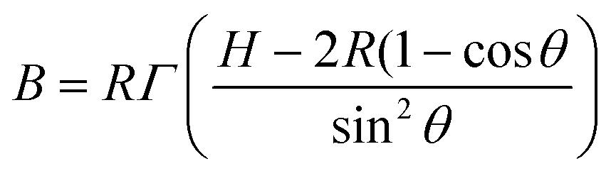 | (1) |
 | ||
| Fig. 2 Measuring bending stiffness through imaging the geometry of curved 2D materials. (a) Schematic showing the heterostructure used for measuring the bending stiffness of graphene. Bilayer graphene was transferred onto the top of an hBN edge step.87 (b–d) Annular dark-field scanning transmission electron microscopy (ADF-STEM) images showing the cross-sectional samples prepared from N-layer graphene samples over H-layer hBN steps. For each designed N and H, a bending profile was measured containing a radius of curvature R, step height H and bending angle θ, indicated in d.87 (e) Plots showing the bending stiffness measured as a function of the thickness of graphene from experiments. Power law relationships are denoted by the red and blue lines just for comparison.87 (f) The experimentally measured (filled symbols) and calculated (open symbols) bending stiffnesses as a function of thickness for few-layer graphene. The blue and red colouring is to show the various bending angles where the data are measured from.87 (g) Calculated contribution to bending stiffness from interfacial interaction, as a function of bending angle, based on simplified Frenkel–Kontorova model. The inset shows that the curvature is accommodated entirely by slip between the layers. Reproduced from ref. 87 with permissions from Springer Nature Limited Copyright 2019.87 | ||
Through varying the step height of the hBN edges (H), the influence of the deformation condition was investigated (Fig. 2c and d). It was found that the experimentally measured B–N curves can be described by a power law dependence (Fig. 2e). Beyond a certain bending angle (>40°), the B–N curves exhibit a nearly linear relationship, characteristic of a stack of frictionless plates, indicating the onset of superlubricity between the graphene atomic layers (Fig. 2f). The reduced bending stiffness at high bending angles can be explained as a result of an increased contribution from an interlayer slip, which can accommodate the large strain at high angles (Fig. 2g).87 It was also found that the bending stiffness of the graphene reaches a minimum when the thickness of the sample is reduced to a monolayer (Fig. 2e). Thus, the thickness of the 2D materials has an important impact on the flexibility of the sample that shall be discussed further in section 4.
3 Microscopy test methods
The size of single-crystal 2D materials is generally limited within a centimetre scale,88–92 depending on the fabrication methods. Taking graphene as an example, the single crystal size is up to 500 μm when prepared by mechanical exfoliation,91 or up to 1 cm size when synthesized by chemical vapour deposition (CVD).14 Therefore, it requires microscopy techniques to reveal the intrinsic mechanical properties of 2D materials, such as nanoindentation experiments under AFM,42,55,92,93 probe push tests under SEM/TEM, and tensile tests conducted based on a micro-electro-mechanical system (MEMS) under SEM/TEM.51,943.1 AFM nanoindentation
The AFM nanoindentation test has been widely applied to examine the intrinsic mechanical properties of 2D materials,63 as well as effects from defects95 and grain boundaries.92 For a typical indentation test set-up, 2D materials were transferred onto a holey substrate (e.g. SiO2/Si) with micro-sized wells. Outside the wells, the continuous graphene membrane is firmly fixed through van der Waals (vdW) attraction to the substrate.96 Inside those wells, 2D materials are suspended as a membrane, where the indentation tests are conducted until fracture happens. From the experiments, the curves of applied force–indentation depth can be directly measured, and most 2D materials show a brittle fracture behaviour. By fitting those curves, E2D can be deduced by the non-linear Föppl membrane theory. Namely, | (2) |
The failure mechanism of 2D materials in response to cyclic and impact loading has been a recent research interest. Fatigue behaviour and damage mechanisms are critical to evaluating the long-term reliability of devices made from 2D materials, because fatigue can cause material failure at stress levels significantly lower than that under static loading. A modified AFM instrument was developed recently to enable applications of both static and cyclic loading to suspended 2D materials. Through adding alternating current inputs using a ‘shake’ piezo (Fig. 3a–c), Cui et al. conducted a fatigue test on graphene and found that it exhibits a fatigue life of more than 109 cycles under a mean stress of 71 GPa, higher than any material reported so far.32 Unlike metals, there is no progressive damage during the fatigue loading of graphene, and its failure is global and catastrophic (see bottom inserts, Fig. 3b). Furthermore, this study illustrates the difference between the morphological changes of bilayer and monolayer graphene during fatigue. Bilayer samples exhibit obvious interlayer shearing and wrinkling after failure, whereas no such behaviour was observed for monolayers after one billion cyclic loadings (Fig. 3c and d). The fatigue behaviour of graphene and graphene oxide (GO) was also compared. In contrast to the catastrophic failure behaviour in graphene, monolayer GO films exhibited localized failure. This could be attributed to the enriched oxygen functional groups in graphene oxide, where epoxide-to-ether transformation can happen during stress loading, which provides trapping sites for cracking arresting, leading to the occurrence of unusual plasticity in graphene oxide.
 | ||
| Fig. 3 Fatigue test conducted on free-standing graphene using AFM.32 (a) A schematic illustrating the set-up for fatigue testing.32 (b) A typical result from a fatigue test conducted on a bilayer graphene under a static loading with a value at half of its fracture force. The abrupt jump in the amplitude and deflection signals at ∼100 million cycles indicate the occurrence of fatigue failure. The insets are AFM images taken before and after the fatigue failure. The diameter of the sample is 2.5 μm. In such a case, the maximum in-plane stress varies from 69.5 to 75.1 GPa calculated using DFT-based nonlinear FEM.32 (c) Normalized elastic modulus E2D of monolayer and bilayer graphene. E2D values are normalized by that measured from the pristine samples without fatigue loading. The red and blue dashed lines are guides to the eye for showing the larger scatter in the E2D for the bilayer compared with monolayer.32 (d) Corresponding cyclic loading-induced wrinkling and local delamination, while no morphological change was observed for the monolayer after cyclic loading. Reproduced from ref. 32 with permissions from Springer Nature Limited Copyright 2020.32 | ||
However, nanoindentation tests have their own limitations. For example, they can only measure a small sample area underneath the indenter tip (tip radii < 50 nm), which does not necessarily represent the properties for the whole membrane.97–99 Also, nanoindentation cannot directly measure fracture strength σ2D. It gives an estimated value of inferred from E2D and δ, using theoretical stress–strain relationships, e.g. with R being the indenter tip radius, assuming a clamped, linear elastic, circular membrane, or σ ∼ δ curves that requires combination with theoretical predictions from density functional theory (DFT) and finite elemental analysis (FEM).32
3.2 In situ probe SEM/TEM bending tests
In the recent two decades, the probe measurements conducted under SEM and TEM, through using in situ pushing set-ups like AFM–TEM and the STM–TEM holders, have been widely used, in particular for understanding the bending behaviour of one-dimensional and three-dimensional samples. For 2D metal chalcogenides, in situ probe tests have been mostly conducted on their bulk counterparts, such as MoS2 and InSe single crystals. For example, combining the experiments with high-throughput calculation, Shi et al. revealed tens of potential 2D metal chalcogenide crystals with plastic deformability, as shown in Fig. 4. Such plasticity is unexpected, as most vdW semiconductors are believed to be brittle because of their weak interlayer forces. Fig. 4c shows a stress–strain curve of InSe taken by SEM compression tests, clearly showing slip-induced strain bursts, similar to those of metals.26 The interlayer slipping energy barrier of InSe is as low as 0.058 eV per atom. In contrast, the cleavage energy is as high as 0.084 eV, such that the constituent layers can maintain integrity during slip, making plastic deformation possible.26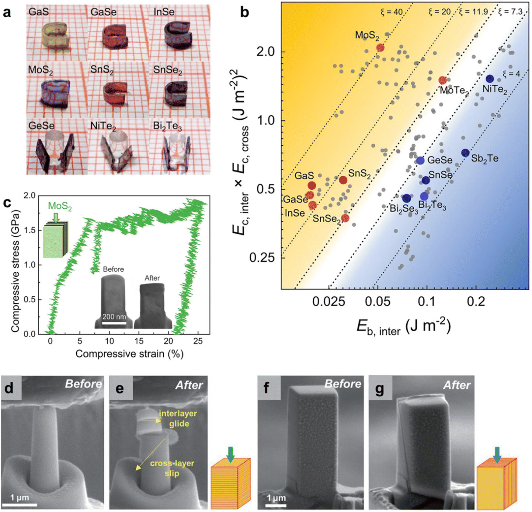 | ||
| Fig. 4 (a) Digital photos of the bent metal chalcogenide samples. The smallest grid is 1 mm.39 (b) A combined index ξ, (Ec,inter × Ec,cross)/Eb,inter to predict 2D vdW materials with plasticity. A plastically deformable 2D vdW crystal should possess a large ξ.39 (c) In situ TEM compression test results, with the top showing stress–strain curves taken from a small micro-machined MoS2 pillar and the bottom part showing TEM images taken before and after the test.39 (d–g) SEM images taken from an in situ SEM compression test on InSe micropillars along (d and e) and perpendicular (f and g) to the (001) axis. Reproduced from ref. 26 with permissions from The American Association for the Advancement of Science Copyright 2020.26 | ||
The in situ probe test can also be used to illustrate the detailed structural evolution process of the 2D metal chalcogenides during deformation, through utilizing the resolution advantages of TEM imaging, i.e. high temporary and spatial resolution. Recently, Zhao et al. directly observed the atomic-scale plasticity mechanism in 2D InSe flakes using an in situ TEM bending test (Fig. 5), with complementary high-resolution STEM imaging.30 It was interesting to see that a phase transition from 2H to 3R occurred in InSe crystals during the deformation (Fig. 5a–c). The in situ characterization studies found that InSe exhibits an unusual plastic deformability, where not only do the interlayer gliding and formation of high-density dislocation networks play a role, but the appearance of numerous discontinuous nanoscale cracks also has an impact, which helps release the increased local elastic energy due to deformation (Fig. 5d–i). Such behaviour distinguishes InSe from other materials such as MoS2, and MoTe2, where large cracks across the whole crystal were observed.30 To illustrate the different deformation behaviour between the materials, further DFT calculations were conducted and indicated that the bonding strength of In–Se (3.855 eV per bond) is weaker than Mo–S (4.368 eV per bond). Therefore, it is relatively easier to break the intralayer In–Se bond, so that the occurrence of cracks is energetically permitted.30 DFT results also explained how phase transition initiates during the deformation of InSe, which suggests that the transition from 2H to 3R in InSe is more energetically favourable compared with those phase transitions in other materials systems such as MoS2 and MoTe2. The above work demonstrates the important role of in situ TEM tests in mechanistic studies for deformation.30
 | ||
| Fig. 5 (a) Digital photos taken from a InSe crystal, before (left panel) and after (right panel) the ex situ compression test.30 (b) High-angle angular dark field-scanning transmission electron microscopy (HAADF-STEM) images taken from InSe crystals, before (left panel) and after (right panel) the ex situ compression test, showing the pristine sample has a 2H phase, while the compressed sample has a 3R phase.30 (c) Schematic showing the experimental set up for the in situ TEM deformation tests. Reproduced from ref. 100 with permissions from The American Association for the Advancement of Science Copyright 2022.100 (d–g) Time-series TEM snapshots, selected from the recorded video taken during the in situ bending experiment, which included TEM images taken before the fracture happens (d), with a corresponding magnified TEM image (e and f) and a rotated and high-resolution TEM image shown in g.30 (h) Corresponding HAADF-STEM images taken before (left panel) and after the in situ experiment.30 (i) Corresponding high-resolution TEM image. The fracture and nanoscale cracks formed at the edge of the sample were marked by a green line and a green box respectively. Reproduced from ref. 30 with permissions from Springer Nature Limited Copyright 2024.30 | ||
However, the application of in situ probe tests for 2D samples is still limited, especially for those atomically-thin ones. The mechanical loading onto a sample is based on a tip with nanometre-scale contact size (see Fig. 5), which is much smaller than the lateral size of most 2D samples while much larger than their thickness, leading to a deformation geometry limited to quasi-1D nanoscrolls. It is therefore remotely possible to use this approach to achieve a controllable and even stress loading, or a quantitative understanding of mechanics in 2D materials. This necessitates the development in micro-electro-mechanical system (MEMS) devices for quantitative experiments, which shall be discussed in the following section.
3.3 Tensile test using MEMS in SEM and TEM
Tensile tests are the most fundamental method to directly measure the fracture strength of bulk materials.94 However, for 2D materials, there are a limited number of research groups doing the in situ tensile tests, due to the technical challenges in the micro-scale sample handling process. The MEMS specific for conducting tensile tests on 2D materials has developed significantly within the recent few years. Such in situ tensile instruments mainly contain a push-to-pull (PTP) micromechanical platform,101 where a push from a pico-indenter generates the force to pull the two ends of a micro-sized 2D sample (Fig. 6). Unlike the nanoindentation tests described in the previous section, MEMS tests apply a uniform uniaxial stress onto the sample and thus enable quantitative measurements of mechanical properties. However, the MEMS-based tests require comparatively complex sample transfer procedures, including the isolation and transfer of suspended 2D materials, and sample shaping using techniques like the focused ion beam (FIB), as illustrated in Fig. 6. The MEMS device is quite similar to other types of suspended 2D device, e.g. acoustic devices, and so are the transfer methods.102 Transfer methods of 2D materials can be classified as wet transfer and dry transfer. Choosing which method is depending on the original substrate of the source 2D materials. Wet transfer is suitable for most source materials regardless of their adhesion to the substrate, as it directly removes or dissolves the original substrate so that the materials can be suspended over a solution. For example, the widely used etchants for dissolving substrates are FeCl3 for copper-supported CVD graphene and KOH for SiOx-supported graphene.103 This suggests both sides of the 2D materials contact and contaminated with a considerable amount of solution, which is not ideal if the purpose is to measure intrinsic mechanical properties by using clean samples. To obtain contamination-free samples, dry transfer has been a major research direction. The dry transfer results in only one side of the 2D materials’ surface being in contact with the solutions or carrying layers, so that the other surface remains intact and clean. Dry transfer is achieved through two approaches: one is adding a water-soluble sacrificing layer, e.g. the widely used a composite layer made by stacking polyvinyl alcohol (PVA) on polymethyl methacrylate (PMMA), and the other is using the ‘dry-stamp’ method, which only applies to those materials that are not strongly adherent to the original substrate e.g. mechanically exfoliated ones. The dry stamp is conducted by removing and transferring the 2D materials from the original substrate to the target substrate, using a carrier layer mostly composed of polymers like poly-dimethylsiloxane (PDMS) and PMMA.104 To further improve the sample cleanliness, a polymer-free transfer would be ideal, for which the composition of the carrying layer has to be changed to non-polymer ones, e.g. metal and ultra-flat SiNx membranes with improved adhesion to the 2D materials.104 However, the dry-stamp methods have rarely been applied to the mechanical test devices of 2D materials, since the stamping force might destroy the MEMS chips, which are mechanically fragile due to the cavity structures. Also, the adhesion between the 2D materials and the MEMS device can be smaller compared with the adhesion to the carrying layer, which makes the success rate of transfer limited. Therefore, it is still challenging to apply dry transfer in the fabrication of MEMS devices105 with contamination-free 2D materials. Nevertheless, through using MEMS in combination with the advances in electron microscopy instruments, quantitative tensile tests have been conducted in a few types of 2D material under TEM and SEM, including hBN,44 graphene,94 TMDs,60,106 transition metal nitrides and carbides,34 and covalent organic frameworks (COFs).107 | ||
| Fig. 6 A schematic showing the typical transfer process for 2D materials samples onto MEMS chips, composed of three steps. (a) The polymer-assisted transfer process onto MEMS chips.28 (b) Removal of the polymer after transfer, confirmed by Raman spectroscopy.28 (c) The clamping and shaping of sample under FIB.28 | ||
The sample quality control is highly important for realizing a reliable and quantitative tensile test on 2D materials.51Fig. 7a shows a schematic of a shaped graphene flake on a tensile testing MEMS chip. By improving sample quality using a modified transfer method, Lu et al. measured a Young's modulus E3D ∼ 900–1000 GPa from a CVD-grown graphene, fairly close to the theoretical value of a pristine monolayer graphene.51 This work approached an elastic strain limit of ∼6% (Fig. 7b), higher than previously reported experimental values. It should be noted that this value ∼6% is still lower compared with the theoretical strain limit of ∼20%, with the representative tensile fracture strength of ∼50–60 GPa measured as being smaller than the ideal strength of monolayer graphene (∼100–130 GPa). This could result from the presence of defects when preparing shaped samples for tensile tests.51 It is well-documented that point defects, line defects, pre-cracks at the sample edge or the sample clamping sites, and oxidized impurities, can be introduced simply due to sample preparation, which leads to considerably reduced strength in 2D materials.32,51,92,94,108 The current shaping methods are generally based on FIB ion milling,109 where ion implantation can lead to surface damage and edge defects in the specimen.51 On the other hand, the transfer of 2D materials with an atomically-thin thickness, especially monolayers, is still challenging due to the low accessibility of the source materials, and the high adhesion of these samples to their original substrates. Very recently, Rong et al. developed a copper mesh-assisted transfer technique, which uses the thin flakes that attached locally to a mesh edge as the source materials.34 The limited attaching area leads to limited adhesion to the substrates, therefore allowing the subsequent transfer of the flakes by FIB nanomanipulation.34 This increases the accessibility to the intrinsic mechanics of monolayer samples. Therefore, to fully understand the fundamental factors that govern the intrinsic mechanical performance of 2D materials, there is much room for improving sample preparation and testing methods.
 | ||
| Fig. 7 Experimental in situ tensile techniques for measuring elastic properties. (a) Schematic showing a single-crystalline graphene sample suspended over the push-to-pull (PTP) micromechanical device. Left top is an SEM image showing an overview of the PTP device actuated by an external pico-indenter. Right top, zoom-in SEM image taken from the region marked by a rectangle in the left-top inset. The yellow arrows indicate the indentation or stress loading direction. Left-bottom inset showing a Raman spectrum taken from the graphene sample. Right-bottom inset showing a TEM bright-field image taken from the sample edge, where an amorphous edge can be observed.51 (b) SEM images taken before and after an in situ tensile test conducted on the suspended graphene.51 (c) Stress–strain curves recorded during the loading and unloading process, in which the arrows denote the emergences and disappearances of the instabilities. The inset is a schematic showing the push-to-shear experimental setup for introducing shearing strain into the 2D materials.31 (d) Time-sequence SEM images taken from the in situ shear test conducted from the monolayer graphene, and the corresponding models describing the sample morphologies during deformation. The top inset is a schematic showing the geometrical parameters of the wrinkling structure.31 (e) Curves present the theoretical normalized wrinkling wavelengths as a function of the shear strains during different stages of instability, in which the solid balls are experimental data points.31 | ||
Meanwhile, there are tensile tests finding that flaw insensitivity exists in 2D materials.53,107 Insensitivity to the pre-existing flaw, such as voids53 and pre-cracks, was observed in hBN and 2D COF.53,107 For example, Han et al. found that the maximum tensile strain of hBN monolayers reaches ∼6%, even though some pre-existing voids were present in the testing samples.53 They found that the naturally occurring voids are not detrimental to the mechanical resistance of hBN. Instead, those defects introduced by FIB to the sample clamped region and the sample edge are responsible for the maximum strain loss of the monolayer. This indicates that the contribution from defects depends on the specific type of the defect and the materials.
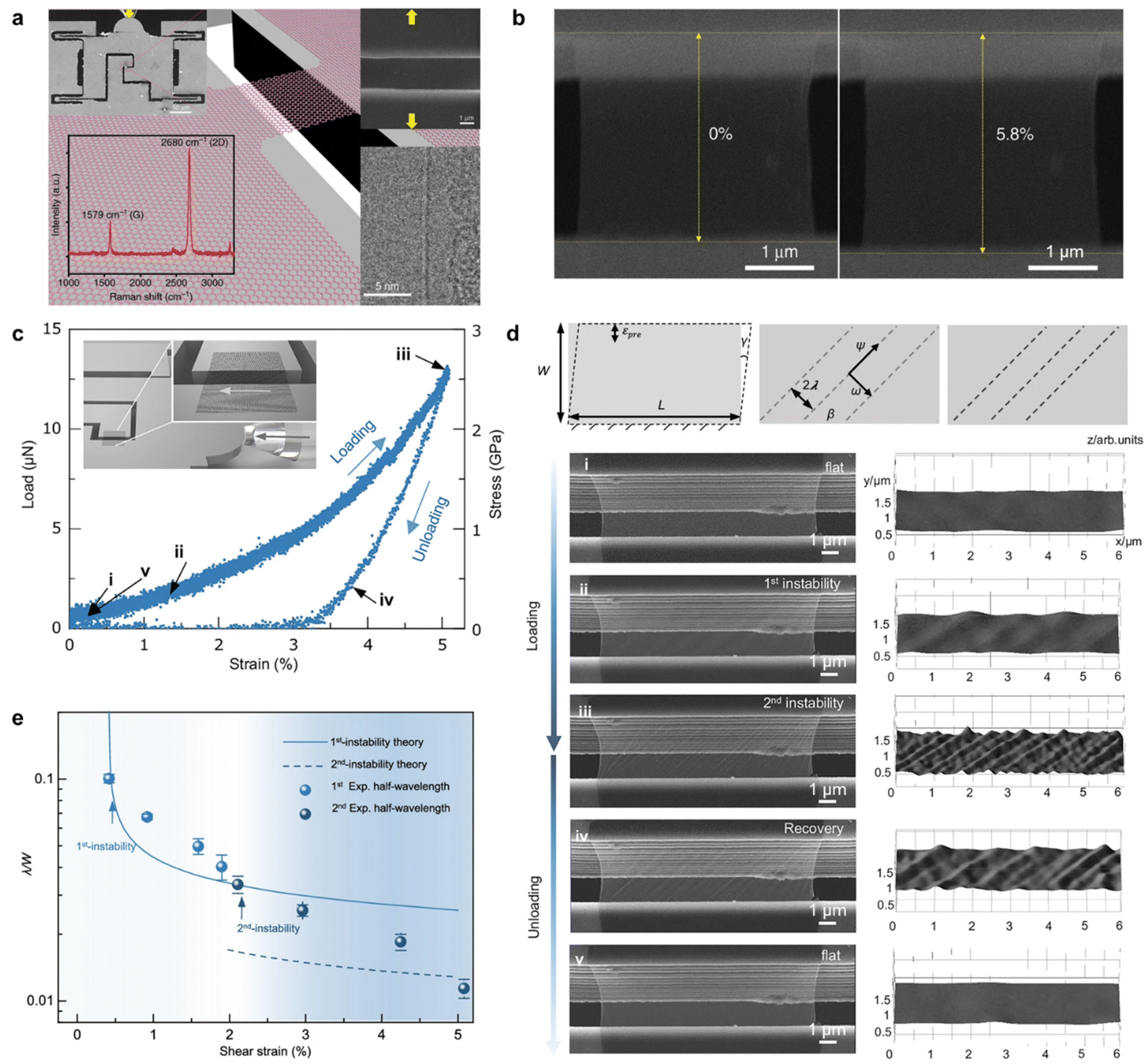
For applications especially in resonator and acoustic devices, it is important to know how the morphology and structure of the 2D materials evolve in real working conditions. Recently, a mechanical push-to-shear approach was developed to illustrate the dynamic wrinkling–splitting–smoothing process of suspended 2D materials (Fig. 7c–e). Shear stress–strain curves of single-layer graphene are shown in Fig. 7c, from which the in-plane shear modulus of the monolayer graphene was determined as ∼70 GPa based on the initial linear stage, slightly larger than the previously measured result, possibly due to the initial corrugations in the sample.110 As illustrated in Fig. 7c and d, during stress loading, the first appearance of wrinkling is marked as the 1st instability. As the shear strain increases beyond a certain threshold, wrinklons are observed with a reducing wavelength of the wrinkles, marked as the 2nd instability, where the wrinkling–splitting happens at a halving of the wavelength, while for the unloading process, the smoothing happens mainly as a result of the reduced amplitude instead of wavelength changing or merging of the wrinkles. Such a difference in stability between the formation and recovery processes can be explained by the redistribution of local compressive stain. The function between D ∼ f(E,εPre,γ)λ4 was also summarized for the initial instability stage, where D denotes the bending stiffness, E denotes the Young's modulus, εpre denotes the pre-tension strain applied on the film, γ denotes the strains, and λ denotes the observed wrinkling wavelength (Fig. 7d and e). The wrinkling wavelength possesses positive correlations with bending stiffness and pre-tension and a negative correlation with Young's modulus and shear strain. Thus, the MEMS in situ tensile test provides a direct pathway to observe and understand the wrinkling behaviour of suspended 2D materials under dynamic stress loading.31
Compared with other in situ methods, the tensile test under TEM has such advantages that it combines the sub-angstrom spatial resolution imaging capability of TEM during the experiments. Fig. 8 shows such a case study conducted by Zhang et al., where the atomic structure at the crack edge was characterized using HRTEM, in combination with the in situ SEM tensile test. It was revealed that the Young's modulus and fracture strength of 2D Ta2NiSe5 (TNS) along the a-axis were measured to be 56.9 ± 9.2 GPa and 2.4 ± 0.8 GPa, respectively, both higher than those along the c-axis (45.0 ± 4.5 GPa and 1.2 ± 0.2 GPa). The correlated high-resolution TEM imaging confirms the crack paths of 2D TNS along different orientations. As shown in Fig. 8a and c, for a TNS sample stretched along the a-axis, the crack edge is sharply formed at an angle of 30° related to the c-axis, and a similar crack structure was observed from the other samples subjected to a 45° counterclockwise rotation (Fig. 8e). In contrast, when the loading direction is parallel to the c-axis (Fig. 8d), a straight crack with an angle of 90° is observed, confirmed by the atomic resolution imaging using TEM. The high-resolution imaging confirms the accuracy of the atomic models used by the subsequent DFT calculation, so that the energetic reasons behind the observed cracking behaviour can be well explained (Fig. 8f).
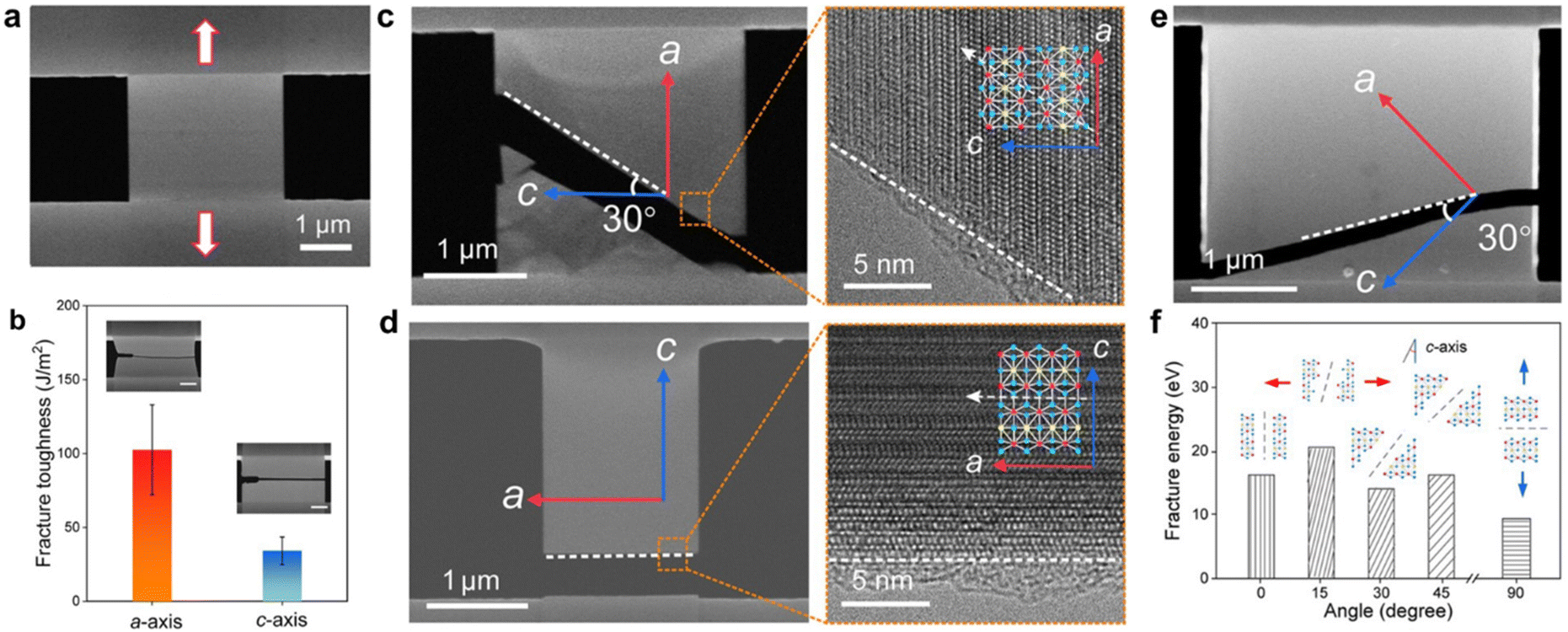 | ||
| Fig. 8 Tensile test conducted on an anisotropic 2D Ta2NiSe5 crystal. (a) An overview SEM image showing Ta2NiSe5 membrane on a “Push-to-Pull” MEMS device.28 (b) Measurements of anisotropic fracture toughness for different samples. Scale bar: 1 μm.28 (c) SEM image taken from a cracked a-axis sample, and a corresponding HRTEM image taken from the crack edge.28 (d) SEM image taken from a cracked sample with its long axis being the c-axis and the corresponding HRTEM image taken from the crack edge.28 (e) SEM image taken from a cracked sample with its axis being 45° to the c-axis.28 (f) DFT calculated fracture toughness using samples cut with various angles to the c-axis direction. Reproduced from ref. 28 with permissions from American Chemical Society Copyright 2024.28 | ||
Despite the as-mentioned developments, there remain few concerns regarding the accuracies of the above microscopy methods, which are often related to sample preparations and displacement measurements. Take the widely used AFM method as an example; since the cantilever is perpendicular to the basal plane of the 2D materials, the atomic layer that contacts the AFM probe may deviate and slip from the normally aligned atomic structure, resulting in a serious mis-arrangement of the atoms and inhomogeneity in the stress field.34 The other controversy still lies in the uncertainty of the sample quality, i.e. the crystal defects and the contamination introduced during sample preparation, e.g. the polymer adsorbent from polymer-assisted 2D sample transfer, the Pt contamination and Ga ion implantation during Pt deposition in the FIB, and the amorphization and artificial cracking due to ion beam damage on 2D samples in the FIB. On the other hand, the data processing for quantitative measurement needs extra care. For instance, the sample thickness is difficult to precisely measure, either on the SiNx membrane device used for AFM nanoindentation, or on the MEMS chips for electron microscopy. These inaccuracies can arise from the contamination added on the top of the sample surface, or simply due to the fact that the substrate has limited flatness, where angstrom-scale inaccuracies can lead to errors when determining the number of atomic layers in the sample. Also, the sample thickness may change before and after the test, and therefore nominal thickness, calculated from an assumed number of atomic layers based on the measurement before testing, is often used, leading to inaccuracies in the calculation of E3D. Besides, the imaging quality during tests is influencing the accuracy of the final results. Take the in situ MEMS SEM/TEM test as an example; the elastic strain of most 2D materials is within 10%, which means the deformation is on a nanometre scale. However, the recording of the in situ test requires a low magnification imaging for the whole sample area. This causes a limitation in pixel resolution and may not satisfy the accuracy required for the measuring the elastic deformation. Therefore, improvements in measurements are still required, especially on sample preparation and imaging techniques such as polymer-free sample transfer104 and correlated imaging.30,38,111
4 Effects of structure
4.1 Thickness
 | ||
| Fig. 9 Fracture and deformation mechanisms under tensile stress. (a) Molecular dynamics (MD) modelling of the failure process of a monolayer graphene with a single-vacancy defect, under a strain rate of 109 s−1, showing bond-stretching failure mode.32 (b) MD modelling of the uniaxial tensile fracture processes of a monolayer MoS2 under a strain rate of 109 s−1, loading along zig zag directions, with the left panel showing the result from elastic strain ε = 0.2735, the middle panel showing ε = 0.3297, and the right panel showing ε = 0.3312. Reproduced from ref. 120 with permissions from IOP Publishing Ltd Copyright 2020.120 (c) Schematic illustration of atomic structure evolution during shear deformation of trilayer graphene, with left panel: initial ABA Bernal structure; middle panel: deformed structure with a rigid lattice with the shear process taking place at the top and bottom layers; right panel: relaxed deformation structure, with the formation of partial dislocations as a result of the low stacking fault energy.115 | ||
 | ||
| Fig. 10 Deformation mechanisms under bending. (a) Bending in graphene that is subjected to various interlayer interactions. The left top panel shows a model where bending is accommodated by in-plane strain. The left bottom panel shows a model where bending is accommodated through interlayer shear and slip. Experimental STEM image taken from a 12-layer graphene bent to 12° (right panel).87 (b–d) Cross-sectional STEM images demonstrating the different ways for 2D materials to accommodate the strain induced by bending. Scale bars, 5 nm. (b) BF STEM image taken from bilayer graphene, with a 95° bend angle. (c) HAADF STEM image showing the formation of a twin structure in multilayer graphite subjected to bending. (d) HAADF STEM image taken from multilayer graphite subjected to a large bending deformation, constituting areas of discrete twin boundaries (orange) and areas of nanotube-like curvature (green).121 | ||
4.2 Defects and grain boundaries
The strength and stretchability of 2D materials are limited by the presence of point and line defects,97,122,123 pre-existing cracks or voids99,111,124 and impurities at the grain boundaries (GBs). Point defects in 2D materials include vacancies where an atom is missing (Fig. 11a), impurities where foreign atoms reside in a substitutional or interstitial site,125 and paired point defects that occurred solely due to local bonding rotation and reconfiguration, such as Stone–Thrower–Wales defects (Fig. 11b), pentagon–heptagon defects125 and pentagon–octagon–pentagon defects.125 Note that those defects can be aligned and extended to constitute topological line defects and grain boundaries.126 Line defects in 2D materials include edge dislocations (Fig. 11d), and screw dislocations (material thickness ≥ bilayer, Fig. 11e and f) that have been observed as a domain wall for phase transition,127 or as a nucleation site for ‘spiral’ 2D materials growth.128,129 | ||
| Fig. 11 Theoretical understanding of a defect's impact on mechanical performance. (a) Schematic atomic model of the vacancies in graphene.123 (b) Schematic atomic model of Stone–Thrower–Wales defects in graphene.123 (c) Tensile strength of graphene at failure, as a function of point vacancy, bivacancy and Stone–Wales defects concentrations in graphene, calculated by MD. Reproduced from ref. 123 with permissions from Elsevier Ltd. Copyright 2013.123 (d) Atomic model showing a pair of edge dislocations observed in graphene by TEM. Reproduced from ref. 135 with permissions from The American Association for the Advancement of Science Copyright 2012.135 (e) Atomic model of screw dislocations with a Burgers vector parallel to a zigzag direction, acting as a 2H|2H domain wall in twisted bilayer TMDs, observed by STEM.127 (f) Atomic model of screw dislocation with a Burgers vector parallel to the out-of-plane direction,136 likely to exist in faulty and disordered graphite. Reproduced from ref. 136 with permissions from American Chemical Society Copyright Copyright 2016.136–138 (g) Atomic models of zigzag-oriented grain boundaries (GBs) in graphene with a tilt angle of 5.5° (left panel), 13.2° (middle panel), and 21.7° (right panel).131 (h) Corresponding MD calculated stress–strain curves of zigzag-oriented graphene sheets pulled perpendicular to the GBs. Reproduced from ref. 131 with permissions from The American Association for the Advancement of Science Copyright 2010.131 | ||
There are two pathways to enhance the strength of the materials: one is to design the arrangement of defects to inhibit dislocation motion or cancel defect effects;130 the other is to go from the opposite: eliminating the defect in crystals using high-quality single-crystal 2D materials. Since it is challenging to prepare large-size single crystal 2D materials for device applications, a usage of polycrystalline 2D crystals is often necessary,131–133 and therefore understanding the role of defects and GBs in mechanical performance is important. There have been theoretical works demonstrating that the detailed arrangement of defects, e.g. the pentagon–heptagon defects associated with graphene GBs, can increase the strength (Fig. 11h),131–133 although it is highly challenging to achieve such a precise defect engineering in materials for real applications.
In contrast to much research interest in theoretical works, the related experimental works on the effects of defect and grain boundaries are of limited quantity. Previous experiments show that presence of GBs provides weak points for oxygen attack111 and impurity segregation, leading to a reduced strength of 2D materials,111 even though careful sample preparation may achieve materials with a strength close to the pristine ones.92 From the perspective of defect types, there are in situ characterization results showing the insensitivity of 2D materials’ stretchability to specific types of defect, as demonstrated in previous sections.53 Regarding the effect of defect density, counter-intuitively, results reported by López-Polín et al. showed that the 2D Young's modulus of graphene increases with an increased density of vacancies created by ion implantation, up to almost twice the initial value when the vacancy content reaches ∼0.2%, as shown in Fig. 12.134 Therefore, controversies still exist regarding the impact of defects on the strength of 2D materials, and more detailed and quantitative studies into defect impacts are needed.
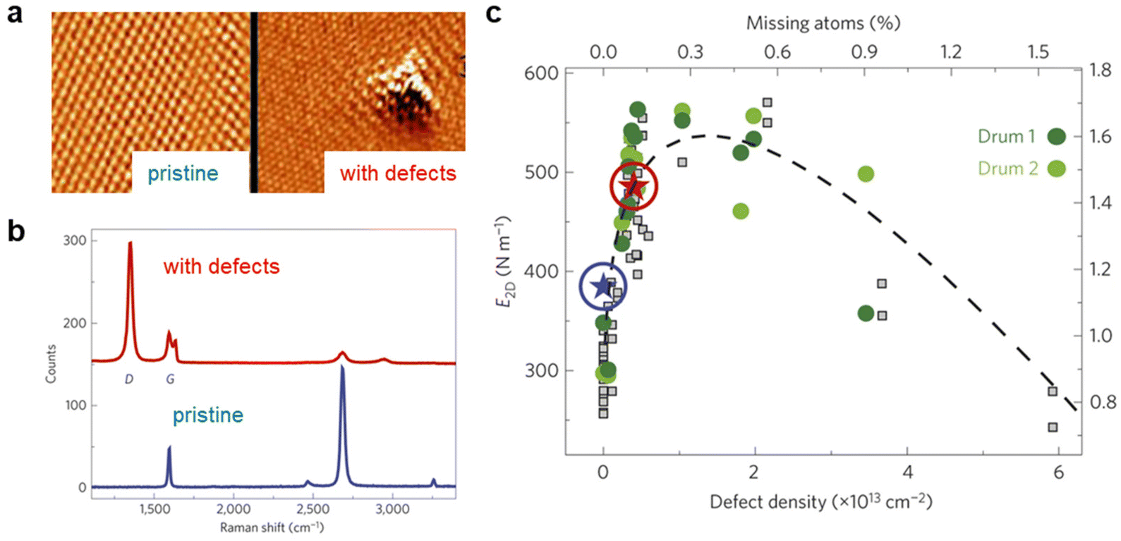 | ||
| Fig. 12 Experimental understanding of a defect's impact on elastic modulus. (a) Atomic-resolution scanning tunnelling microscopy (STM) characterization of a pristine graphene, before Ar+ irradiation (left panel), and after irradiation, which shows a single defect containing a vacancy cluster (right panel).134 (b) Raman spectra taken from the sample before and after the irradiation treatment, denoted by blue and red colours respectively. The intensity ratio between the D and G peaks can be used to evaluate to defect density.134 (c) E2D measured by AFM nanoindentation as a function of defect concentration. Reproduced from ref. 134 with permissions from Springer Nature Limited Copyright 2014.134 | ||
4.3 Interfaces
Extensive interest has been put into exploring vdW heterostructures and homostructures, which are a unique class of artificial solids that can be stacked like ‘Lego’, allowing controllable material components, stacking order and relative twist angle between adjacent atomic layers. Significant breakthroughs have been achieved in vdW heterostructures, including the observation of low-temperature superconductivity in twisted bilayer graphene, and localization of excitons in twisted bilayer TMDs.127 This makes mechanics studies of vdW heterostructures timely and important.However, fracture mechanics of vdW heterostructures have been quite limited.45,56,139,140 The E2D of the bilayer heterostructure is lower than the sum of the E2D of each layer but comparable to the corresponding bilayers, when a strong interlayer interaction is achieved (Fig. 13). Nevertheless, the interlayer interaction varies with the material components (e.g. MoS2–WS2 interaction > MoS2-graphene), and can only be as strong as a homo-bilayer when the interface is clean or coherent (lattice matching). The MD calculation reported showed that local delamination/buckling can happen when the heterostructure is loaded with a large tensile strain (Fig. 13e).
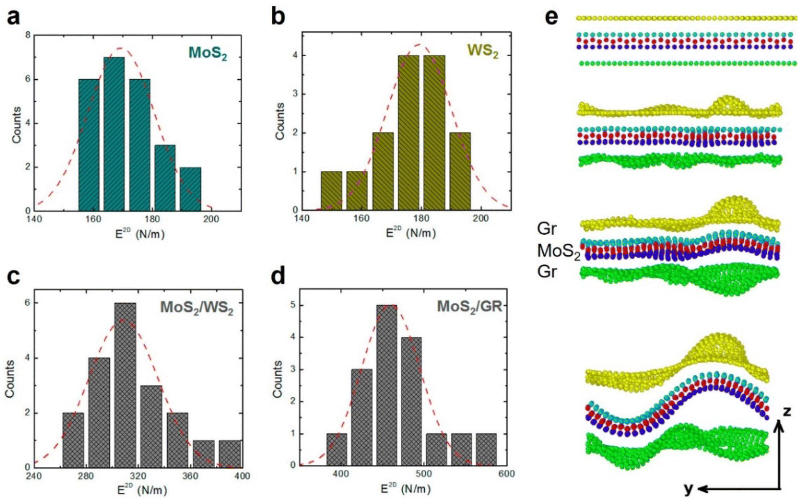 | ||
| Fig. 13 Elastic properties and fracture failure mechanism in vdW heterostructures. (a–d) Experimentally measured elastic properties for CVD-grown MoS2 and WS2 monolayers, and their stacked bilayer heterostructure. (a) Histogram of E2D for CVD MoS2 nanoplates. (b) Histogram of E2D for CVD WS2 triangular nanoplates. (c) Histogram of E2D for a CVD MoS2/WS2 heterostructure. (d) Histogram of E2D for a CVD MoS2/Gr heterostructure. Reproduced from ref. 56 with permissions from American Chemical Society Copyright 2014.56 (e) MD calculated tensile deformation process for a graphene–MoS2–graphene heterostructure, which shows buckling at the ultimate strain ε = 0.26 at 1.0 K. From top to bottom, the tension in the x direction increases. Reproduced from ref. 139 with permissions from AIP Publishing Copyright 2014.139 | ||
In fact, the interlayer interaction between the stacked components varies with the stacking method and the twist angle.56 In a twisted heterostructure, for a twist angle close to 0° (identical to n × 60° with n being an integer, in hexagonal-symmetry 2D materials), lattice matching induces commensurate lattices at the interface, where the interlayer interaction is stronger141 compared with the incommensurate interface formed at twist angles deviating from n × 60°. Friction experiments prove that superlubricity exists at graphene–hBN heterostructure interfaces for specific twist angles (e.g. 30°, 90°, 150°) where the interface is incommensurate (Fig. 14). This used the other mechanical loading mode of AFM, which is nanofriction with the tip moving parallel to the material surface, and meanwhile the horizontal change caused by the frictional force is recorded by the piezoelectric ceramic transducer, suitable for studying the interface characteristics of 2D materials. In contrast, for those twist angles retaining high symmetry (0°, 60°, 120° etc.), the interface structure can be commensurate and the friction is found to be much higher (Fig. 14).142
 | ||
| Fig. 14 Measuring the friction at the interface of a graphite/hBN heterostructure. (a) Schematic diagram of the experimental set-up to measure the friction in graphite/hBN junctions.142 (b) Schematic atomic model shows the stress loading onto the graphite/hBN heterostructures during the friction experiments.142 (c) Dependence of the frictional stress on the relative interfacial orientation between monocrystalline graphite and hBN measured under ambient conditions. Reproduced from ref. 142 with permissions from Springer Nature Limited Copyright 2018.142 | ||
Taking advantage of the superlubricity between heterostructures, Huang et al. investigated how the bending stiffness of 2D heterostructures evolves with the composition of the stack,33 following the bending stiffness measurement work shown in section 2. They fabricated four-layer graphene/MoS2 heterostructures with varied component sequences, including Gr/MoS2/Gr/MoS2 (denoted as GMGM here) and Gr/Gr/MoS2/MoS2 (GGMM) heterostructures (Fig. 15). MGGM, GMMG, and MMGG show a strong bending angle dependence in bending stiffness. In contrast, the bending stiffness of GMGM exhibits no dependence on the bending angle. At high bending angles, the bending stiffnesses of all four structures converge to approximately 20–25 eV. At low bending angles, the measured bending stiffness is much higher for structures with more aligned interfaces, i.e. those containing MM or GG (Fig. 15d). The interfacial friction can be further reduced by large-angle twisting, and the bending stiffness of the resulted heterostructures is largely lower by over several hundred percent compared with other heterostructures. This demonstrates the importance of interfacial engineering in achieving a flexible 2D multilayer, where a minimum bending stiffness can be achieved through misaligning heterointerfaces.
 | ||
| Fig. 15 Bending of four-layer 2D heterostructures, composed of various orders of graphene (G) and MoS2 (M) layers. (a) Schematic of a heterostructure draped over an atomically sharp step of hBN.33 (b–e) Cross-sectional ADF-STEM images of four different 2D heterostructures (GMGM, MGGM, GMMG, and MMGG) with an identical composition but different stacking orders. Scale bars: 2 nm.33 (f) Plot of bending stiffness for each heterostructure, coloured by bending angle. Reproduced from ref. 33 with permissions from Wiley-VCH GmbH Copyright 2021.33 | ||
5 Applications
The properties of 2D materials can be changed by strain engineering. To prepare deformed 2D materials, a wide range of approaches has been reported. Besides the direct strain loading methods described in sections 2 and 3, one can induce the in-plane deformation using the lattice mismatch at an interface of a heterostructure,90 or at the interface with a substrate.143,144 Artificial stress can also be applied through force transfer from the supporting substrate or polymer matrix.115 The out-of-plane deformation can be induced by coherent epitaxy growth,145 using a substrate with patterned 3D features,146,147 or a stretchable substrate processed with tension.148,149 Besides, the strain applied to the 2D materials can be utilized to fabricate crystals with unusual atomic stackings. For example, rhombohedral stacked graphite can be accessed through applying additional shear force during exfoliation150,151 or during CVD growth on a curved substrate.152 TMDs with a large-area 3R stacking that is normally thermodynamically metastable can be achieved by internal strain relaxation occurring during the twisting of 2D heterostructures.127To achieve 2D material composites with enhanced flexibility, recent developments on aligning strategy have enabled the rational design of the spatial alignment of 2D materials. Taking graphene fibre as an instance, previous reports have proved the importance of the alignment of graphene sheets to enhance the mechanical properties. This has been achieved through modifying liquid processing parameters, such as shear flow and enlarged crystal concentration in liquid crystal precursors.153 However, the assembly of sheets remains loose in the transverse direction of the fibre. To improve the order in transverse directions, Gao et al. realized the concentric arrangement of graphene oxide nanosheets instead of a random structure through applying a multiple shear flow field. An increased assembly order is achieved through introducing a rotating angular velocity imposed by rotational shear flow (Fig. 16a).38 Please note that such an angular velocity–assembly order relationship is non-monotonic. Theoretical modelling indicates that when the angular velocity is too high, the excessive centrifugal force makes the radial pressure gradient and viscous force unable to suppress the disturbance in the flow, resulting in a secondary vortex velocity field and a spiral arrangement with defects.38 Indeed, experiments show that a higher or lower angular velocity results in the formation of helical disorder or random disorder, which can be characterized by the Hermans orientation function, accounting for the lower thermal conductivity and Young's modulus.38 Through optimizing the angular velocity, combined with tuning of polymer components in the composites, they achieved an enhanced assembly order in both the longitudinal and transverse directions, and thus synergistically improved and extraordinary mechanical and thermal properties.38 The above study indicates that it is necessary to correlate the theoretical mechanics with the assembly techniques of 2D flakes for rationally designed structural 2D materials with enhanced mechanical and functional properties.
 | ||
| Fig. 16 (a) Rationally constructed high-strength and thermally conductive graphene oxide fibre. The top panel is a schematic showing the sheet-order in the spinning tube under the unidirectional flow field (denoted as Plane I) and the aligned graphene oxide sheets under the multiple flow fields (Planes II and III). The middle panel displays the cross-sectional views of the velocity distributions, calculated under unidirectional tubular shear-flow field (left), and under multiple shear flow with moderate (middle) and overhigh (right) rotating angular velocities. The bottom left panel displays the velocity distribution across the spinning tube calculated under multiple shear-flow with a rotating angular velocity of 100 rad s−1 (left) and 1000 rad s−1 (right). The bottom middle panel shows the experimentally measured density and orientation order of the graphene fibres. The bottom right panel shows the stress–strain curve measured from the graphene fibres.38 (b) The top left panel is a digital photo taken from the flexible substrate integrated with hundreds of WS2 devices. The top right panel is a schematic showing the strain distribution within the WS2 device under a biaxial strain. The bottom left panel shows the increased mobility as a function of the strain applied to WS2. Bottom right is a DFT calculation of conduction bands from monolayer WS2 structures built without strain (black line), with 1% uniaxial strain (dashed blue line), and 1% biaxial strain (dashed orange line) relative to the lowest band edge. The inset is a schematic of the unit cell structure used for the simulation with applied strain vectors. Reproduced from ref. 167 with permissions from American Chemical Society Copyright 2024.167 (c) Quantum photon emitters fabricated from strain-engineered monolayer and bilayer WSe2. The left panel is an optical image taken after transfer onto the nanopillars. The right panel is a spatial mapping showing the intensity integrated from the as-measured photoluminescence spectrum between 700–860 nm. Reproduced from ref. 157 with permissions from Springer Nature Limited Copyright 2022.157,179 (d) Ferroelectricity due to strain in CuInP2S6. The top left panel shows a schematic of the device structure. The top right panel presents an amplitude map showing the domain wall structure imaged by band excitation piezo-response force microscopy. The bottom panel displays a schematic for the bent nanoflake on the patterned substrate. Reproduced from ref. 172 with permissions from American Chemical Society Copyright 2023.172 | ||
Deformation has been demonstrated as an established approach to tune the electronic and optical properties of 2D materials, including mobility, photon emitting and ferroelectricity.154–156 Quite a few theories and experiments have found that strain engineering can be utilized to increase the electron mobility of 2D semiconductors, which allows their applications in flexible electronics and sensors.157–166 Recently, Yang et al. developed a force loading approach that enables a biaxial tensile strain in 2D MoS2 and WS2.167 Compared with the case of uniaxial tensile strain, the mobility of WS2 can be much higher in biaxial strain status (Fig. 16b).167 DFT calculations reveal that this resulted from a reduced bandgap as well as a reduced intervalley electron–phonon scattering.167 For optoelectronic applications, single-photon emitters (SPEs) created by strained 2D materials, including hBN, WSe2, WS2, and MoTe2, have attracted much interest in the recent decade.157,159,168–170 This was achieved by suspending 2D semiconductors over arrays of nano-pillars.159 For example, WSe2 SPEs were created through transferring a WSe2 flake on top of lithographically defined nanopillars, where point-like defect or strain perturbations locally change the bandgap and lead to quantum confinement of excitons (Fig. 16c). The performance of the 2D semiconductor SPEs can be modulated by changing the strain applied to the 2D semiconductors. For example, Ferrari et al. show that quantum-light emitters with deterministic positions surpass their randomly distributed counterparts, in which case the spectral wanderings were reduced by an order of magnitude.158 Recently, Chen et al. reported that a large local strain of up to 5% in WSe2 can increase the brightness of the resulting SPEs.168 They further improved the emitting stability through tightly attaching the 2D semiconductor to the surface of the pillar with enhanced fitting.168 On the other hand, curvature and strain effects are also important for ferroelectric 2D materials, such as In2Se3, CuInP2S6, and Bi2TeO5, and various twisted hetero/homostructures.100,118,171–177 Enhanced polarization is expected under a large curvature.171,175 Taking CuInP2S6 as an example, it was observed that ferroelectric domain boundaries tend to form near or move towards the high-curvature areas, and the polarization–voltage hysteresis loops in the bending regions differ from the non-bending regions (Fig. 16d).172 The above studies all indicate that achieving precise strain modulation in 2D materials is a crucial strategy for enhancing their performance in electronic and optical devices.157,167,172,178
6 Conclusions
In spite of the above progress, studies in the characterization of bendable 2D materials are still in their infancy, with many opportunities and challenges ahead, as summarized in Fig. 17. From the materials’ perspective, the limited success in the high-quality transfer of 2D materials onto target substrates, especially onto their characterization platforms like MEMS chips, hinders the investigation into the mechanics of a wider range of 2D materials. The development of handling of 2D materials for experimental mechanics study needs combination with the polymer-free and site-specific transfer methods recently developed for 2D electronics, so that the experiments can reflect the intrinsic properties of the thin materials. Nevertheless, benefiting from the new techniques for the assembly of 2D materials, either vertically or axially, accessibility to materials and devices with high flexibility and enhanced device performances is enlarged nowadays. This allowed the design of the bending stiffness of 2D heterostructures or composites based on a controllable stacking order. Developments in theoretical mechanics are also important for achieving the rational assembly of 2D composites and thus devices with new functionalities. Microscopic studies on characterization methods for mechanics in 2D materials, especially on their response to dynamic stress loading, are necessary in order to understand the mechanical stability of 2D materials for application in resonators and acoustic devices. This further opens the prospects for the development of instruments for quantitative stress loading. Furthermore, correlated imaging is highly needed so that the advantages of various microscopy techniques, such as electron microscopy and optical imaging, can be combined to achieve in situ studies with both high spatial and temporal resolutions. It should be noted that the in situ imaging protocols specific for 2D materials are not well-established, compared with those for one-dimensional or three-dimensional materials. Mechanisms behind the deformation of 2D materials are not studied systematically considering the controversies and complex effects from defects and interlayer interactions, and have only been investigated for limited types of 2D material. Finally, since those 2D materials with plasticity have their irreplaceability in flexible electronics, the route of integrating them into devices with maintained flexibility and the mechanisms behind the plastic deformation still need exploration.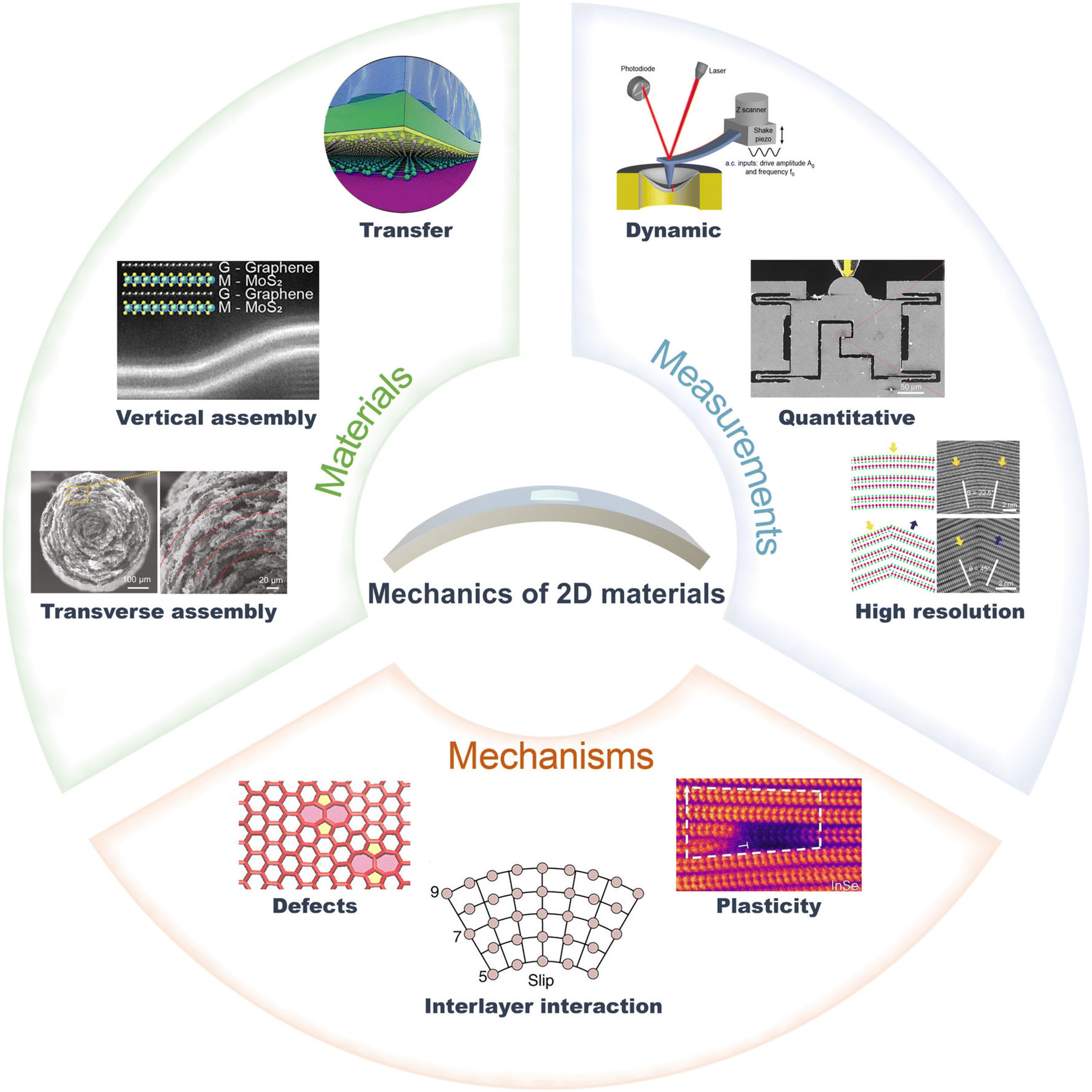 | ||
| Fig. 17 Strategies and prospects for characterization studies of mechanics in 2D materials. Reproduced from ref. 118 with permissions from American Chemical Society Copyright 2023.30,32,33,38,51,87,104,118,123 | ||
Data availability
No primary research results, software or code have been included and no new data were generated or analysed as part of this review.Conflicts of interest
There are no conflicts of interest to declare.Acknowledgements
This work is supported by the National Natural Science Foundation of China (Grant No. 12474026, 12104517), the Natural Science Foundation of Guangdong Province (Basic and Applied Basic Research Foundation 2023A1515011465) and the Young Top Talents Program 2021QN02C068.References
- K. S. Novoselov, A. K. Geim, S. V. Morozov, D. Jiang, Y. Zhang, S. V. Dubonos, I. V. Grigorieva and A. A. Firsov, Science, 2004, 306, 666–669 CrossRef CAS PubMed.
- N. Mounet, M. Gibertini, P. Schwaller, D. Campi, A. Merkys, A. Marrazzo, T. Sohier, I. E. Castelli, A. Cepellotti, G. Pizzi and N. Marzari, Nat. Nanotechnol., 2018, 13, 246–252 CrossRef CAS PubMed.
- S. B. Desai, S. R. Madhvapathy, A. B. Sachid, J. P. Llinas, Q. Wang, G. H. Ahn, G. Pitner, M. J. Kim, J. Bokor, C. Hu, H.-S. P. Wong and A. Javey, Science, 2016, 354, 99–102 CrossRef CAS PubMed.
- B. Radisavljevic, A. Radenovic, J. Brivio, V. Giacometti and A. Kis, Nat. Nanotechnol., 2011, 6, 147–150 Search PubMed.
- J. Zhang, N. Kong, S. Uzun, A. Levitt, S. Seyedin, P. A. Lynch, S. Qin, M. Han, W. Yang, J. Liu, X. Wang, Y. Gogotsi and J. M. Razal, Adv. Mater., 2020, 32, 2001093 Search PubMed.
- C. R. Dean, A. F. Young, I. Meric, C. Lee, L. Wang, S. Sorgenfrei, K. Watanabe, T. Taniguchi, P. Kim, K. L. Shepard and J. Hone, Nat. Nanotechnol., 2010, 5, 722–726 CrossRef CAS PubMed.
- L. Britnell, R. M. Ribeiro, A. Eckmann, R. Jalil, B. D. Belle, A. Mishchenko, Y.-J. Kim, R. V. Gorbachev, T. Georgiou, S. V. Morozov, A. N. Grigorenko, A. K. Geim, C. Casiraghi, A. H. C. Neto and K. S. Novoselov, Science, 2013, 340, 1311–1314 CrossRef CAS PubMed.
- F. Withers, O. Del Pozo-Zamudio, A. Mishchenko, A. P. Rooney, A. Gholinia, K. Watanabe, T. Taniguchi, S. J. Haigh, A. K. Geim, A. I. Tartakovskii and K. S. Novoselov, Nat. Mater., 2015, 14, 301–306 CrossRef CAS PubMed.
- N. Lindahl, D. Midtvedt, J. Svensson, O. A. Nerushev, N. Lindvall, A. Isacsson and E. E. B. Campbell, Nano Lett., 2012, 12, 3526–3531 CrossRef CAS PubMed.
- P. Blake, P. D. Brimicombe, R. R. Nair, T. J. Booth, D. Jiang, F. Schedin, L. A. Ponomarenko, S. V. Morozov, H. F. Gleeson, E. W. Hill, A. K. Geim and K. S. Novoselov, Nano Lett., 2008, 8, 1704–1708 CrossRef PubMed.
- R. R. Nair, P. Blake, A. N. Grigorenko, K. S. Novoselov, T. J. Booth, T. Stauber, N. M. R. Peres and A. K. Geim, Science, 2008, 320, 1308–1308 CrossRef CAS PubMed.
- P. Z. Sun, Q. Yang, W. J. Kuang, Y. V. Stebunov, W. Q. Xiong, J. Yu, R. R. Nair, M. I. Katsnelson, S. J. Yuan, I. V. Grigorieva, M. Lozada-Hidalgo, F. C. Wang and A. K. Geim, Nature, 2020, 579, 229–232 CrossRef CAS PubMed.
- M. F. El-Kady, V. Strong, S. Dubin and R. B. Kaner, Science, 2012, 335, 1326–1330 CrossRef CAS PubMed.
- K. S. Kim, Y. Zhao, H. Jang, S. Y. Lee, J. M. Kim, K. S. Kim, J.-H. Ahn, P. Kim, J.-Y. Choi and B. H. Hong, Nature, 2009, 457, 706–710 CrossRef CAS PubMed.
- J. N. Coleman, M. Lotya, A. O'Neill, S. D. Bergin, P. J. King, U. Khan, K. Young, A. Gaucher, S. De, R. J. Smith, I. V. Shvets, S. K. Arora, G. Stanton, H.-Y. Kim, K. Lee, G. T. Kim, G. S. Duesberg, T. Hallam, J. J. Boland, J. J. Wang, J. F. Donegan, J. C. Grunlan, G. Moriarty, A. Shmeliov, R. J. Nicholls, J. M. Perkins, E. M. Grieveson, K. Theuwissen, D. W. McComb, P. D. Nellist and V. Nicolosi, Science, 2011, 331, 568–571 CrossRef CAS PubMed.
- Y. Hernandez, V. Nicolosi, M. Lotya, F. M. Blighe, Z. Sun, S. De, I. T. McGovern, B. Holland, M. Byrne, Y. K. Gun'Ko, J. J. Boland, P. Niraj, G. Duesberg, S. Krishnamurthy, R. Goodhue, J. Hutchison, V. Scardaci, A. C. Ferrari and J. N. Coleman, Nat. Nanotechnol., 2008, 3, 563–568 CrossRef CAS PubMed.
- S. Bae, H. Kim, Y. Lee, X. Xu, J.-S. Park, Y. Zheng, J. Balakrishnan, T. Lei, H. Ri Kim, Y. I. Song, Y.-J. Kim, K. S. Kim, B. Özyilmaz, J.-H. Ahn, B. H. Hong and S. Iijima, Nat. Nanotechnol., 2010, 5, 574–578 CrossRef CAS PubMed.
- D. Akinwande, N. Petrone and J. Hone, Nat. Commun., 2014, 5, 5678 CrossRef CAS PubMed.
- J. Yao and G. Yang, Small, 2018, 14, 1704524 CrossRef PubMed.
- F. Liu, W. T. Navaraj, N. Yogeswaran, D. H. Gregory and R. Dahiya, ACS Nano, 2019, 13, 3257–3268 CrossRef CAS PubMed.
- U. Khan, T.-H. Kim, H. Ryu, W. Seung and S.-W. Kim, Adv. Mater., 2017, 29, 1603544 CrossRef PubMed.
- E. O. Polat, G. Mercier, I. Nikitskiy, E. Puma, T. Galan, S. Gupta, M. Montagut, J. J. Piqueras, M. Bouwens, T. Durduran, G. Konstantatos, S. Goossens and F. Koppens, Sci. Adv., 2019, 5, eaaw7846 CrossRef CAS PubMed.
- S. K. Ameri, R. Ho, H. Jang, L. Tao, Y. Wang, L. Wang, D. M. Schnyer, D. Akinwande and N. Lu, ACS Nano, 2017, 11, 7634–7641 CrossRef PubMed.
- G. Anagnostopoulos, P.-N. Pappas, Z. Li, I. A. Kinloch, R. J. Young, K. S. Novoselov, C. Y. Lu, N. Pugno, J. Parthenios, C. Galiotis and K. Papagelis, ACS Appl. Mater. Interfaces, 2016, 8, 22605–22614 CrossRef CAS PubMed.
- J. Ryu, Y. Kim, D. Won, N. Kim, J. S. Park, E.-K. Lee, D. Cho, S.-P. Cho, S. J. Kim, G. H. Ryu, H.-A. S. Shin, Z. Lee, B. H. Hong and S. Cho, ACS Nano, 2014, 8, 950–956 CrossRef CAS PubMed.
- T.-R. Wei, M. Jin, Y. Wang, H. Chen, Z. Gao, K. Zhao, P. Qiu, Z. Shan, J. Jiang, R. Li, L. Chen, J. He and X. Shi, Science, 2020, 369, 542–545 CrossRef CAS PubMed.
- A. K. Katiyar, A. T. Hoang, D. Xu, J. Hong, B. J. Kim, S. Ji and J.-H. Ahn, Chem. Rev., 2024, 124, 318–419 CrossRef CAS PubMed.
- B. Li, J. Li, W. Jiang, Y. Wang, D. Wang, L. Song, Y. Zhu, H. Wu, G. Wang and Z. Zhang, Nano Lett., 2024, 24, 6344–6352 CrossRef CAS PubMed.
- Y. Yang, B. Liang, J. Kreie, M. Hambsch, Z. Liang, C. Wang, S. Huang, X. Dong, L. Gong, C. Liang, D. Lou, Z. Zhou, J. Lu, Y. Yang, X. Zhuang, H. Qi, U. Kaiser, S. C. B. Mannsfeld, W. Liu, A. Gölzhäuser and Z. Zheng, Nature, 2024, 630, 878–883 CrossRef CAS PubMed.
- L. W. Wong, K. Yang, W. Han, X. Zheng, H. Y. Wong, C. S. Tsang, C.-S. Lee, S. P. Lau, T. H. Ly, M. Yang and J. Zhao, Nat. Mater., 2024, 23, 196–204 CrossRef CAS PubMed.
- Y. Hou, J. Zhou, Z. He, J. Chen, M. Zhu, H. Wu and Y. Lu, Nat. Commun., 2024, 15, 4033 CrossRef CAS PubMed.
- T. Cui, S. Mukherjee, P. M. Sudeep, G. Colas, F. Najafi, J. Tam, P. M. Ajayan, C. V. Singh, Y. Sun and T. Filleter, Nat. Mater., 2020, 19, 405–411 CrossRef CAS PubMed.
- J. Yu, E. Han, M. A. Hossain, K. Watanabe, T. Taniguchi, E. Ertekin, A. M. van der Zande and P. Y. Huang, Adv. Mater., 2021, 33, 2007269 CrossRef CAS PubMed.
- C. Rong, T. Su, Z. Li, T. Chu, M. Zhu, Y. Yan, B. Zhang and F.-Z. Xuan, Nat. Commun., 2024, 15, 1566 CrossRef CAS PubMed.
- H. Tang, Y. Wang, X. Ni, K. Watanabe, T. Taniguchi, P. Jarillo-Herrero, S. Fan, E. Mazur, A. Yacoby and Y. Cao, Nature, 2024, 632, 1038–1044 CrossRef CAS PubMed.
- A. J. Mannix, A. Ye, S. H. Sung, A. Ray, F. Mujid, C. Park, M. Lee, J.-H. Kang, R. Shreiner, A. A. High, D. A. Muller, R. Hovden and J. Park, Nat. Nanotechnol., 2022, 17, 361–366 CrossRef CAS PubMed.
- M. Nakatani, S. Fukamachi, P. Solís-Fernández, S. Honda, K. Kawahara, Y. Tsuji, Y. Sumiya, M. Kuroki, K. Li, Q. Liu, Y.-C. Lin, A. Uchida, S. Oyama, H. G. Ji, K. Okada, K. Suenaga, Y. Kawano, K. Yoshizawa, A. Yasui and H. Ago, Nat. Electron., 2024, 7, 119–130 CrossRef.
- P. Li, Z. Wang, Y. Qi, G. Cai, Y. Zhao, X. Ming, Z. Lin, W. Ma, J. Lin, H. Li, K. Shen, Y. Liu, Z. Xu, Z. Xu and C. Gao, Nat. Commun., 2024, 15, 409 CrossRef CAS PubMed.
- Z. Gao, T.-R. Wei, T. Deng, P. Qiu, W. Xu, Y. Wang, L. Chen and X. Shi, Nat. Commun., 2022, 13, 7491 CrossRef CAS PubMed.
- Z. Dai, L. Liu and Z. Zhang, Adv. Mater., 2019, 31, 1805417 CrossRef CAS PubMed.
- C. Si, Z. Sun and F. Liu, Nanoscale, 2016, 8, 3207–3217 RSC.
- C. Lee, X. Wei, J. W. Kysar and J. Hone, Science, 2008, 321, 385–388 CrossRef CAS PubMed.
- M. Z. Miskin, K. J. Dorsey, B. Bircan, Y. Han, D. A. Muller, P. L. McEuen and I. Cohen, Proc. Natl. Acad. Sci. U. S. A., 2018, 115, 466–470 CrossRef CAS PubMed.
- Y. Yang, Z. Song, G. Lu, Q. Zhang, B. Zhang, B. Ni, C. Wang, X. Li, L. Gu, X. Xie, H. Gao and J. Lou, Nature, 2021, 594, 57–61 CrossRef CAS PubMed.
- C. Androulidakis, K. Zhang, M. Robertson and S. Tawfick, 2D Mater., 2018, 5, 032005 CrossRef.
- M. Holwill, Nanomechanics in van der Waals heterostructures, Springer, Cham, 2019 Search PubMed.
- A. Castellanos-Gomez, V. Singh, H. S. J. van der Zant and G. A. Steele, Ann. Phys., 2015, 527, 27–44 CrossRef CAS.
- J. Tan, H. Zhang, X. Wang, Y. Wang, J.-J. Wang, H. Zhang, E. Ma and W. Zhang, Mater. Today, 2024, 80, 250–261 CrossRef CAS.
- Y. Sun, J. Pan, Z. Zhang, K. Zhang, J. Liang, W. Wang, Z. Yuan, Y. Hao, B. Wang, J. Wang, Y. Wu, J. Zheng, L. Jiao, S. Zhou, K. Liu, C. Cheng, W. Duan, Y. Xu, Q. Yan and K. Liu, Nano Lett., 2019, 19, 761–769 CrossRef CAS PubMed.
- A. Falin, Q. Cai, E. J. Santos, D. Scullion, D. Qian, R. Zhang, Z. Yang, S. Huang, K. Watanabe, T. Taniguchi, M. R. Barnett, Y. Chen, R. S. Ruoff and L. H. Li, Nat. Commun., 2017, 8, 15815 CrossRef CAS PubMed.
- K. Cao, S. Feng, Y. Han, L. Gao, T. H. Ly, Z. Xu and Y. Lu, Nat. Commun., 2020, 11, 284 CrossRef CAS PubMed.
- G. Wang, Z. Dai, Y. Wang, P. Tan, L. Liu, Z. Xu, Y. Wei, R. Huang and Z. Zhang, Phys. Rev. Lett., 2017, 119, 036101 CrossRef PubMed.
- Y. Han, S. Feng, K. Cao, Y. Wang, L. Gao, Z. Xu and Y. Lu, Cell Rep. Phys. Sci., 2020, 1, 100172 CrossRef CAS.
- G. Wang, Z. Dai, J. Xiao, S. Feng, C. Weng, L. Liu, Z. Xu, R. Huang and Z. Zhang, Phys. Rev. Lett., 2019, 123, 116101 CrossRef CAS PubMed.
- S. Bertolazzi, J. Brivio and A. Kis, ACS Nano, 2011, 5, 9703–9709 CrossRef CAS PubMed.
- K. Liu, Q. Yan, M. Chen, W. Fan, Y. Sun, J. Suh, D. Fu, S. Lee, J. Zhou, S. Tongay, J. Ji, J. B. Neaton and J. Wu, Nano Lett., 2014, 14, 5097–5103 CrossRef CAS PubMed.
- D. Lloyd, X. Liu, N. Boddeti, L. Cantley, R. Long, M. L. Dunn and J. S. Bunch, Nano Lett., 2017, 17, 5329–5334 CrossRef CAS PubMed.
- N. Iguiñiz, R. Frisenda, R. Bratschitsch and A. Castellanos-Gomez, Adv. Mater., 2019, 31, 1807150 CrossRef PubMed.
- Y. Li, C. Yu, Y. Gan, P. Jiang, J. Yu, Y. Ou, D.-F. Zou, C. Huang, J. Wang, T. Jia, Q. Luo, X.-F. Yu, H. Zhao, C.-F. Gao and J. Li, npj Comput. Mater., 2018, 4, 49 CrossRef.
- Y. Yang, X. Li, M. Wen, E. Hacopian, W. Chen, Y. Gong, J. Zhang, B. Li, W. Zhou, P. M. Ajayan, Q. Chen, T. Zhu and J. Lou, Adv. Mater., 2017, 29, 1604201 CrossRef PubMed.
- V. Babacic, D. S. Reig, S. Varghese, T. Vasileiadis, E. Coy, K.-J. Tielrooij and B. Graczykowski, Adv. Mater., 2021, 33, 2008614 CrossRef CAS PubMed.
- J. Li, N. V. Medhekar and V. B. Shenoy, J. Phys. Chem. C, 2013, 117, 15842–15848 CrossRef CAS.
- R. Zhang, V. Koutsos and R. Cheung, Appl. Phys. Lett., 2016, 108, 042104 CrossRef.
- A. Falin, M. Holwill, H. Lv, W. Gan, J. Cheng, R. Zhang, D. Qian, M. R. Barnett, E. J. G. Santos, K. S. Novoselov, T. Tao, X. Wu and L. H. Li, ACS Nano, 2021, 15, 2600–2610 CrossRef CAS PubMed.
- H. Wang, E. J. Sandoz-Rosado, S. H. Tsang, J. Lin, M. Zhu, G. Mallick, Z. Liu and E. H. T. Teo, Adv. Funct. Mater., 2019, 29, 1902663 CrossRef.
- Y. M. Jahn and A. Ya'Akobovitz, Nanoscale, 2021, 13, 18458–18466 Search PubMed.
- G. Wang, Z. Zhang, Y. Wang, E. Gao, X. Jia, Z. Dai, C. Weng, L. Liu, Y. Zhang and Z. Zhang, ACS Appl. Mater. Interfaces, 2021, 13, 3040–3050 CrossRef CAS PubMed.
- Y. Li, C. Yu, Y. Gan, Y. Kong, P. Jiang, D.-F. Zou, P. Li, X.-F. Yu, R. Wu and H. Zhao, Nanotechnology, 2019, 30, 335703 CrossRef CAS PubMed.
- B. Chitara and A. Ya'Akobovitz, Nanoscale, 2018, 10, 13022–13027 RSC.
- L. Guo, H. Yan, Q. Moore, M. Buettner, J. Song, L. Li, P. T. Araujo and H.-T. Wang, Nanoscale, 2015, 7, 11915–11921 RSC.
- H. Yan, C. Vajner, M. Kuhlman, L. Guo, L. Li, P. T. Araujo and H.-T. Wang, Appl. Phys. Lett., 2016, 109, 032103 CrossRef.
- J.-Y. Wang, Y. Li, Z.-Y. Zhan, T. Li, L. Zhen and C.-Y. Xu, Appl. Phys. Lett., 2016, 108, 013104 Search PubMed.
- B. Zhang, L. Zhang, N. Yang, X. Zhao, C. Chen, Y. Cheng, I. Rasheed, L. Ma and J. Zhang, J. Phys. Chem. C, 2022, 126, 1094–1098 CrossRef CAS.
- A. Lipatov, H. Lu, M. Alhabeb, B. Anasori, A. Gruverman, Y. Gogotsi and A. Sinitskii, Sci. Adv., 2018, 4, eaat0491 CrossRef PubMed.
- A. Lipatov, M. Alhabeb, H. Lu, S. Zhao, M. Loes, N. Vorobeva, Y. Dall'Agnese, Y. Gao, A. Gruverman, Y. Gogotsi and A. Sinitskii, Adv. Electron. Mater., 2020, 6, 1901382 Search PubMed.
- A. Castellanos-Gomez, M. Poot, A. Amor-Amorós, G. A. Steele, H. S. J. van der Zant, N. Agraït and G. Rubio-Bollinger, Nano Res., 2012, 5, 550–557 CrossRef CAS.
- Q. Hao, C. Zhao, B. Sun, C. Lu, J. Liu, M. Liu, L.-J. Wan and D. Wang, J. Am. Chem. Soc., 2018, 140, 12152–12158 CrossRef CAS PubMed.
- Z. Zeng, I. S. Flyagina and J.-C. Tan, Nanoscale Adv., 2020, 2, 5181–5191 RSC.
- Q. Tu, I. Spanopoulos, P. Yasaei, C. C. Stoumpos, M. G. Kanatzidis, G. S. Shekhawat and V. P. Dravid, ACS Nano, 2018, 12, 10347–10354 CrossRef CAS PubMed.
- W. Chen, U. Khan, S. Feng, B. Ding, X. Xu and B. Liu, Adv. Funct. Mater., 2020, 30, 2004960 CrossRef CAS.
- M. Šiškins, S. Kurdi, M. Lee, B. J. M. Slotboom, W. Xing, S. Mañas-Valero, E. Coronado, S. Jia, W. Han, T. van der Sar, H. S. J. van der Zant and P. G. Steeneken, npj 2D Mater. Appl., 2022, 6, 41 CrossRef.
- F. Cantos-Prieto, A. Falin, M. Alliati, D. Qian, R. Zhang, T. Tao, M. R. Barnett, E. J. Santos, L. H. Li and E. Navarro-Moratalla, Nano Lett., 2021, 21, 3379–3385 CrossRef CAS PubMed.
- M. Šiškins, M. Lee, F. Alijani, M. R. van Blankenstein, D. Davidovikj, H. S. J. van der Zant and P. G. Steeneken, ACS Nano, 2019, 13, 10845–10851 CrossRef PubMed.
- T. Hu, J. Yang, W. Li, X. Wang and C. M. Li, Phys. Chem. Chem. Phys., 2020, 22, 2115–2121 RSC.
- Y. Wei, B. Wang, J. Wu, R. Yang and M. L. Dunn, Nano Lett., 2013, 13, 26–30 CrossRef CAS PubMed.
- X. Chen, C. Yi and C. Ke, Appl. Phys. Lett., 2015, 106, 101907 CrossRef.
- E. Han, J. Yu, E. Annevelink, J. Son, D. A. Kang, K. Watanabe, T. Taniguchi, E. Ertekin, P. Y. Huang and A. M. van der Zande, Nat. Mater., 2020, 19, 305–309 CrossRef CAS PubMed.
- Y. Huang, Y.-H. Pan, R. Yang, L.-H. Bao, L. Meng, H.-L. Luo, Y.-Q. Cai, G.-D. Liu, W.-J. Zhao, Z. Zhou, L.-M. Wu, Z.-L. Zhu, M. Huang, L.-W. Liu, L. Liu, P. Cheng, K.-H. Wu, S.-B. Tian, C.-Z. Gu, Y.-G. Shi, Y.-F. Guo, Z. G. Cheng, J.-P. Hu, L. Zhao, G.-H. Yang, E. Sutter, P. Sutter, Y.-L. Wang, W. Ji, X.-J. Zhou and H.-J. Gao, Nat. Commun., 2020, 11, 2453 CrossRef CAS PubMed.
- M. Velický, G. E. Donnelly, W. R. Hendren, S. McFarland, D. Scullion, W. J. I. DeBenedetti, G. C. Correa, Y. Han, A. J. Wain, M. A. Hines, D. A. Muller, K. S. Novoselov, H. D. Abruña, R. M. Bowman, E. J. G. Santos and F. Huang, ACS Nano, 2018, 12, 10463–10472 CrossRef PubMed.
- X. Li, M.-W. Lin, J. Lin, B. Huang, A. A. Puretzky, C. Ma, K. Wang, W. Zhou, S. T. Pantelides, M. Chi, I. Kravchenko, J. Fowlkes, C. M. Rouleau, D. B. Geohegan and K. Xiao, Sci. Adv., 2016, 2, e1501882 CrossRef PubMed.
- Y. Huang, E. Sutter, N. N. Shi, J. Zheng, T. Yang, D. Englund, H.-J. Gao and P. Sutter, ACS Nano, 2015, 9, 10612–10620 CrossRef CAS PubMed.
- G.-H. Lee, R. C. Cooper, S. J. An, S. Lee, A. van der Zande, N. Petrone, A. G. Hammerberg, C. Lee, B. Crawford, W. Oliver, J. W. Kysar and J. Hone, Science, 2013, 340, 1073–1076 CrossRef CAS PubMed.
- A. Castellanos-Gomez, M. Poot, G. A. Steele, H. S. J. van der Zant, N. Agraït and G. Rubio-Bollinger, Nanoscale Res. Lett., 2012, 7, 233 CrossRef PubMed.
- P. Zhang, L. Ma, F. Fan, Z. Zeng, C. Peng, P. E. Loya, Z. Liu, Y. Gong, J. Zhang, X. Zhang, P. M. Ajayan, T. Zhu and J. Lou, Nat. Commun., 2014, 5, 3782 CrossRef CAS PubMed.
- A. Zandiatashbar, G.-H. Lee, S. J. An, S. Lee, N. Mathew, M. Terrones, T. Hayashi, C. R. Picu, J. Hone and N. Koratkar, Nat. Commun., 2014, 5, 3186 CrossRef PubMed.
- S. P. Koenig, N. G. Boddeti, M. L. Dunn and J. S. Bunch, Nat. Nanotechnol., 2011, 6, 543–546 CrossRef CAS PubMed.
- Z. Song, V. I. Artyukhov, J. Wu, B. I. Yakobson and Z. Xu, ACS Nano, 2015, 9, 401–408 CrossRef CAS PubMed.
- J. Han, N. M. Pugno and S. Ryu, Nanoscale, 2015, 7, 15672–15679 RSC.
- G. López-Polín, J. Gómez-Herrero and C. Gómez-Navarro, Nano Lett., 2015, 15, 2050–2054 CrossRef PubMed.
- X. Zheng, W. Han, K. Yang, L. W. Wong, C. S. Tsang, K. H. Lai, F. Zheng, T. Yang, S. P. Lau, T. H. Ly, M. Yang and J. Zhao, Sci. Adv., 2022, 8, eabo0773 CrossRef CAS PubMed.
- S. R. Sadanand, B. J. Cheol, Y. G. Yeol, R. Jae-Kyung, L. C. Jun, H. Seong-Gu, B. Sachin and K. T. Nam, Korean J. Mater. Res., 2018, 28, 627–632 CrossRef.
- Z. Wan, H. Liu, Y. Zheng, Y. Ma, K. Liu, X. Zhou, C. Liu, K. Liu and E. Wang, Adv. Funct. Mater., 2024, 34, 2303519 CrossRef CAS.
- T. F. Schranghamer, M. Sharma, R. Singh and S. Das, Chem. Soc. Rev., 2021, 50, 11032–11054 RSC.
- W. Wang, N. Clark, M. Hamer, A. Carl, E. Tovari, S. Sullivan-Allsop, E. Tillotson, Y. Gao, H. de Latour, F. Selles, J. Howarth, E. G. Castanon, M. Zhou, H. Bai, X. Li, A. Weston, K. Watanabe, T. Taniguchi, C. Mattevi, T. H. Bointon, P. V. Wiper, A. J. Strudwick, L. A. Ponomarenko, A. V. Kretinin, S. J. Haigh, A. Summerfield and R. Gorbachev, Nat. Electron., 2023, 6, 981–990 CrossRef CAS.
- M. J. Hamer, D. G. Hopkinson, N. Clark, M. Zhou, W. Wang, Y. Zou, D. J. Kelly, T. H. Bointon, S. J. Haigh and R. V. Gorbachev, Nano Lett., 2020, 20, 6582–6589 CrossRef CAS PubMed.
- P. Li, C. Jiang, S. Xu, Y. Zhuang, L. Gao, A. Hu, H. Wang and Y. Lu, Nanoscale, 2017, 9, 9119–9128 RSC.
- Q. Fang, C. Sui, C. Wang, T. Zhai, J. Zhang, J. Liang, H. Guo, E. Sandoz-Rosado and J. Lou, Matter, 2021, 4, 1017–1028 CrossRef CAS.
- D. G. Papageorgiou, I. A. Kinloch and R. J. Young, Prog. Mater. Sci., 2017, 90, 75–127 CrossRef CAS.
- K. L. Firestein, J. E. von Treifeldt, D. G. Kvashnin, J. F. S. Fernando, C. Zhang, A. G. Kvashnin, E. V. Podryabinkin, A. V. Shapeev, D. P. Siriwardena, P. B. Sorokin and D. Golberg, Nano Lett., 2020, 20, 5900–5908 CrossRef CAS PubMed.
- X. Liu, T. H. Metcalf, J. T. Robinson, B. H. Houston and F. Scarpa, Nano Lett., 2012, 12, 1013–1017 CrossRef CAS PubMed.
- Z. Li, R. J. Young, C. Backes, W. Zhao, X. Zhang, A. Zhukov, E. Tillotson, A. P. Conlan, F. Ding, S. J. Haigh, K. S. Novoselov and J. N. Coleman, ACS Nano, 2020, 14, 10976–10985 CrossRef CAS PubMed.
- K. Min and N. R. Aluru, Appl. Phys. Lett., 2011, 98, 013113 CrossRef.
- L. He, S. Guo, J. Lei, Z. Sha and Z. Liu, Carbon, 2014, 75, 124–132 CrossRef CAS.
- H. Yin, H. J. Qi, F. Fan, T. Zhu, B. Wang and Y. Wei, Nano Lett., 2015, 15, 1918–1924 CrossRef CAS PubMed.
- L. Gong, R. J. Young, I. A. Kinloch, S. J. Haigh, J. H. Warner, J. A. Hinks, Z. Xu, L. Li, F. Ding, I. Riaz, R. Jalil and K. S. Novoselov, ACS Nano, 2013, 7, 7287–7294 CrossRef CAS PubMed.
- I. V. Lebedeva, A. V. Lebedev, A. M. Popov and A. A. Knizhnik, Phys. Rev. B, 2016, 93, 235414 CrossRef.
- P. Li, K. Cao, C. Jiang, S. Xu, L. Gao, X. Xiao and Y. Lu, Nanotechnology, 2019, 30, 475708 CrossRef CAS PubMed.
- E. Han, S. M. Nahid, T. Rakib, G. Nolan, P. F. Ferrari, M. A. Hossain, A. Schleife, S. Nam, E. Ertekin, A. M. van der Zande and P. Y. Huang, ACS Nano, 2023, 17, 7881–7888 CrossRef CAS PubMed.
- D.-M. Tang, D. G. Kvashnin, S. Najmaei, Y. Bando, K. Kimoto, P. Koskinen, P. M. Ajayan, B. I. Yakobson, P. B. Sorokin, J. Lou and D. Golberg, Nat. Commun., 2014, 5, 3631 CrossRef PubMed.
- C. Yi, C. Hu, M. Bai, J. Lv and D. Tang, Nanotechnology, 2020, 31, 215703 CrossRef CAS PubMed.
- A. P. Rooney, Z. Li, W. Zhao, A. Gholinia, A. Kozikov, G. Auton, F. Ding, R. V. Gorbachev, R. J. Young and S. J. Haigh, Nat. Commun., 2018, 9, 3597 CrossRef CAS PubMed.
- V. Sorkin, Q. X. Pei and Y. W. Zhang, in Handbook of Materials Modeling: Applications: Current and Emerging Materials, ed. W. Andreoni and S. Yip, Springer International Publishing, Cham, 2020, pp. 1869–1909 Search PubMed.
- B. Mortazavi and S. Ahzi, Carbon, 2013, 63, 460–470 CrossRef CAS.
- C. Cao, S. Mukherjee, J. Y. Howe, D. D. Perovic, Y. Sun, C. V. Singh and T. Filleter, Sci. Adv., 2018, 4, eaao7202 CrossRef PubMed.
- H. Terrones, R. Lv, M. Terrones and M. S. Dresselhaus, Rep. Prog. Phys., 2012, 75, 062501 CrossRef PubMed.
- J. Lahiri, Y. Lin, P. Bozkurt, I. I. Oleynik and M. Batzill, Nat. Nanotechnol., 2010, 5, 326–329 CrossRef CAS PubMed.
- A. Weston, Y. Zou, V. Enaldiev, A. Summerfield, N. Clark, V. Zólyomi, A. Graham, C. Yelgel, S. Magorrian, M. Zhou, J. Zultak, D. Hopkinson, A. Barinov, T. H. Bointon, A. Kretinin, N. R. Wilson, P. H. Beton, V. I. Fal'ko, S. J. Haigh and R. Gorbachev, Nat. Nanotechnol., 2020, 15, 592–597 CrossRef CAS PubMed.
- T. H. Ly, J. Zhao, H. Kim, G. H. Han, H. Nam and Y. H. Lee, Adv. Mater., 2016, 28, 7723–7728 CrossRef CAS PubMed.
- R. Y. Tay, H. J. Park, J. Lin, Z. K. Ng, L. Jing, H. Li, M. Zhu, S. H. Tsang, Z. Lee and E. H. T. Teo, Chem. Mater., 2018, 30, 6858–6866 CrossRef CAS.
- T. Deng, Z. Gao, Z. Li, P. Qiu, Z. Li, X. Yuan, C. Ming, T.-R. Wei, L. Chen and X. Shi, Science, 2024, 386, 1112–1117 CrossRef CAS PubMed.
- R. Grantab, V. B. Shenoy and R. S. Ruoff, Science, 2010, 330, 946–948 CrossRef CAS PubMed.
- Y. Wei, J. Wu, H. Yin, X. Shi, R. Yang and M. Dresselhaus, Nat. Mater., 2012, 11, 759–763 CrossRef CAS PubMed.
- T.-H. Liu, C.-W. Pao and C.-C. Chang, Carbon, 2012, 50, 3465–3472 CrossRef CAS.
- G. López-Polín, C. Gómez-Navarro, V. Parente, F. Guinea, M. I. Katsnelson, F. Pérez-Murano and J. Gómez-Herrero, Nat. Phys., 2015, 11, 26–31 Search PubMed.
- J. H. Warner, E. R. Margine, M. Mukai, A. W. Robertson, F. Giustino and A. I. Kirkland, Science, 2012, 337, 209–212 CrossRef CAS PubMed.
- F. Xu, H. Yu, A. Sadrzadeh and B. I. Yakobson, Nano Lett., 2016, 16, 34–39 CrossRef CAS PubMed.
- I. Suarez-Martinez, G. Savini, G. Haffenden, J. M. Campanera and M. I. Heggie, Phys. Status Solidi C, 2007, 4, 2958–2962 CrossRef CAS.
- J. W. Martin, C. de Tomas, I. Suarez-Martinez, M. Kraft and N. A. Marks, Phys. Rev. Lett., 2019, 123, 116105 CrossRef CAS PubMed.
- J.-W. Jiang and H. S. Park, Appl. Phys. Lett., 2014, 105, 033108 CrossRef.
- T. Mukhopadhyay, A. Mahata, S. Adhikari and M.A. Zaeem, Nanoscale, 2018, 10, 5280–5294 RSC.
- J. Zhang, J. Wang, P. Chen, Y. Sun, S. Wu, Z. Jia, X. Lu, H. Yu, W. Chen, J. Zhu, G. Xie, R. Yang, D. Shi, X. Xu, J. Xiang, K. Liu and G. Zhang, Adv. Mater., 2016, 28, 1950–1956 CrossRef CAS PubMed.
- Y. Song, D. Mandelli, O. Hod, M. Urbakh, M. Ma and Q. Zheng, Nat. Mater., 2018, 17, 894–899 CrossRef CAS PubMed.
- G. H. Ahn, M. Amani, H. Rasool, D.-H. Lien, J. P. Mastandrea, J. W. Ager III, M. Dubey, D. C. Chrzan, A. M. Minor and A. Javey, Nat. Commun., 2017, 8, 608 CrossRef PubMed.
- Y. K. Ryu, F. Carrascoso, R. López-Nebreda, N. Agraït, R. Frisenda and A. Castellanos-Gomez, Nano Lett., 2020, 20, 5339–5345 CrossRef CAS PubMed.
- S. Xie, L. Tu, Y. Han, L. Huang, K. Kang, K. U. Lao, P. Poddar, C. Park, D. A. Muller, R. A. DiStasio and J. Park, Science, 2018, 359, 1131–1136 CrossRef CAS PubMed.
- J. Choi, H. J. Kim, M. C. Wang, J. Leem, W. P. King and S. Nam, Nano Lett., 2015, 15, 4525–4531 CrossRef CAS PubMed.
- Y. Zhang, M. Heiranian, B. Janicek, Z. Budrikis, S. Zapperi, P. Y. Huang, H. T. Johnson, N. R. Aluru, J. W. Lyding and N. Mason, Nano Lett., 2018, 18, 2098–2104 CrossRef CAS PubMed.
- A. Castellanos-Gomez, R. Roldán, E. Cappelluti, M. Buscema, F. Guinea, H. S. J. van der Zant and G. A. Steele, Nano Lett., 2013, 13, 5361–5366 CrossRef CAS PubMed.
- Y. Wang, R. Yang, Z. Shi, L. Zhang, D. Shi, E. Wang and G. Zhang, ACS Nano, 2011, 5, 3645–3650 CrossRef CAS PubMed.
- S. Huang, G. Zhang, F. Fan, C. Song, F. Wang, Q. Xing, C. Wang, H. Wu and H. Yan, Nat. Commun., 2019, 10, 2447 CrossRef PubMed.
- J. P. Nery, M. Calandra and F. Mauri, Nano Lett., 2020, 20, 5017–5023 CrossRef CAS PubMed.
- Z. Gao, S. Wang, J. Berry, Q. Zhang, J. Gebhardt, W. M. Parkin, J. Avila, H. Yi, C. Chen, S. Hurtado-Parra, M. Drndić, A. M. Rappe, D. J. Srolovitz, J. M. Kikkawa, Z. Luo, M. C. Asensio, F. Wang and A. T. C. Johnson, Nat. Commun., 2020, 11, 546 CrossRef CAS PubMed.
- A. Akbari, P. Sheath, S. T. Martin, D. B. Shinde, M. Shaibani, P. C. Banerjee, R. Tkacz, D. Bhattacharyya and M. Majumder, Nat. Commun., 2016, 7, 10891 CrossRef CAS PubMed.
- Y. Dong, M.-M. Yang, M. Yoshii, S. Matsuoka, S. Kitamura, T. Hasegawa, N. Ogawa, T. Morimoto, T. Ideue and Y. Iwasa, Nat. Nanotechnol., 2023, 18, 36–41 CrossRef CAS PubMed.
- J. Zhu, S. Wu, L. Wang, J. Wu, J. Zhu, L. Zou, F. Xiao, Z. Su, C. Jiao, S. Pei, Z. Zhang, J. Qin, B. Xu, Y. Zhou, J. Xia and Z. Wang, InfoMat, 2024, 6, e12553 CrossRef CAS.
- X. Fan, Z. Chen, D. Xu, L. Zou, F. Ouyang, S. Deng, X. Wang, J. Zhao and Y. Zhou, Adv. Funct. Mater., 2024, 34, 2404750 CrossRef CAS.
- M. Turunen, M. Brotons-Gisbert, Y. Dai, Y. Wang, E. Scerri, C. Bonato, K. D. Jöns, Z. Sun and B. D. Gerardot, Nat. Rev. Phys., 2022, 4, 219–236 CrossRef.
- C. Palacios-Berraquero, D. M. Kara, A. R. P. Montblanch, M. Barbone, P. Latawiec, D. Yoon, A. K. Ott, M. Loncar, A. C. Ferrari and M. Atatüre, Nat. Commun., 2017, 8, 15093 CrossRef CAS PubMed.
- M. Koperski, K. Nogajewski, A. Arora, V. Cherkez, P. Mallet, J. Y. Veuillen, J. Marcus, P. Kossacki and M. Potemski, Nat. Nanotechnol., 2015, 10, 503–506 CrossRef CAS PubMed.
- S. Kumar, A. Kaczmarczyk and B. D. Gerardot, Nano Lett., 2015, 15, 7567–7573 CrossRef CAS PubMed.
- L. N. Tripathi, O. Iff, S. Betzold, Ł. Dusanowski, M. Emmerling, K. Moon, Y. J. Lee, S.-H. Kwon, S. Höfling and C. Schneider, ACS Photonics, 2018, 5, 1919–1926 CrossRef CAS.
- M. Brooks and G. Burkard, Phys. Rev. B, 2018, 97, 195454 CrossRef CAS.
- W. Zhao, Z. Ghorannevis, K. K. Amara, J. R. Pang, M. Toh, X. Zhang, C. Kloc, P. H. Tan and G. Eda, Nanoscale, 2013, 5, 9677–9683 RSC.
- Q. H. Wang, K. Kalantar-Zadeh, A. Kis, J. N. Coleman and M. S. Strano, Nat. Nanotechnol., 2012, 7, 699–712 CrossRef CAS PubMed.
- A. Srivastava, M. Sidler, A. V. Allain, D. S. Lembke, A. Kis and A. Imamoğlu, Nat. Nanotechnol., 2015, 10, 491–496 CrossRef CAS PubMed.
- T. T. Tran, K. Bray, M. J. Ford, M. Toth and I. Aharonovich, Nat. Nanotechnol., 2016, 11, 37–41 CrossRef CAS PubMed.
- J. A. Yang, R. K. A. Bennett, L. Hoang, Z. Zhang, K. J. Thompson, A. Michail, J. Parthenios, K. Papagelis, A. J. Mannix and E. Pop, ACS Nano, 2024, 18, 18151–18159 CrossRef CAS PubMed.
- S. Chen, C. Wang, H. Cai, L. Ma, Y. Qu, Z. Liu, S. Wang, J. Zhan, Q. Tan, B. Sheng, X. Liu, X. Wang, X. Zhang, J. Xu, W. Gao and Q. Liu, Matter, 2024, 7, 1106–1116 CrossRef CAS.
- Y.-M. He, G. Clark, J. R. Schaibley, Y. He, M.-C. Chen, Y.-J. Wei, X. Ding, Q. Zhang, W. Yao, X. Xu, C.-Y. Lu and J.-W. Pan, Nat. Nanotechnol., 2015, 10, 497–502 CrossRef CAS PubMed.
- T. Cai, J.-H. Kim, Z. Yang, S. Dutta, S. Aghaeimeibodi and E. Waks, ACS Photonics, 2018, 5, 3466–3471 CrossRef CAS.
- W. Ming, B. Huang, S. Zheng, Y. Bai, J. Wang, J. Wang and J. Li, Sci. Adv., 2022, 8, eabq1232 CrossRef CAS PubMed.
- Y. Liu, A. N. Morozovska, A. Ghosh, K. P. Kelley, E. A. Eliseev, J. Yao, Y. Liu and S. Kalinin, ACS Nano, 2023, 17, 22004–22014 CrossRef PubMed.
- X. Jiang, X. Wang, X. Wang, X. Zhang, R. Niu, J. Deng, S. Xu, Y. Lun, Y. Liu, T. Xia, J. Lu and J. Hong, Nat. Commun., 2022, 13, 574 CrossRef CAS PubMed.
- M. Han, C. Wang, K. Niu, Q. Yang, C. Wang, X. Zhang, J. Dai, Y. Wang, X. Ma, J. Wang, L. Kang, W. Ji and J. Lin, Nat. Commun., 2022, 13, 5903 CrossRef CAS PubMed.
- C. Chen, H. Liu, Q. Lai, X. Mao, J. Fu, Z. Fu and H. Zeng, Nano Lett., 2022, 22, 3275–3282 CrossRef CAS PubMed.
- A. Weston, E. G. Castanon, V. Enaldiev, F. Ferreira, S. Bhattacharjee, S. Xu, H. Corte-León, Z. Wu, N. Clark, A. Summerfield, T. Hashimoto, Y. Gao, W. Wang, M. Hamer, H. Read, L. Fumagalli, A. V. Kretinin, S. J. Haigh, O. Kazakova, A. K. Geim, V. I. Fal'ko and R. Gorbachev, Nat. Nanotechnol., 2022, 17, 390–395 CrossRef CAS PubMed.
- Y. Zhou, D. Wu, Y. Zhu, Y. Cho, Q. He, X. Yang, K. Herrera, Z. Chu, Y. Han, M. C. Downer, H. Peng and K. Lai, Nano Lett., 2017, 17, 5508–5513 CrossRef CAS PubMed.
- Q. Liu, W. Wang, H. Sinhmar, I. Griniasty, J. Z. Kim, J. T. Pelster, P. Chaudhari, M. F. Reynolds, M. C. Cao, D. A. Muller, A. B. Apsel, N. L. Abbott, H. Kress-Gazit, P. L. McEuen and I. Cohen, Nat. Mater., 2025, 24, 109–115 CrossRef CAS PubMed.
- A. Branny, S. Kumar, R. Proux and B. D. Gerardot, Nat. Commun., 2017, 8, 15053 CrossRef CAS PubMed.
| This journal is © The Royal Society of Chemistry 2025 |