
Improved electronic uniformity and nanoscale homogeneity in template-grown CsPbBr3 nanorods†
Eduardo
Avila-Lopez
 a,
Shuang
Liang
b,
Isaac
Elias
a,
Zhiqun
Lin
*bc and
Yize Stephanie
Li
*a
a,
Shuang
Liang
b,
Isaac
Elias
a,
Zhiqun
Lin
*bc and
Yize Stephanie
Li
*a
aSchool of Natural Sciences, Mathematics, and Engineering, California State University, Bakersfield, California 93311, USA. E-mail: yli11@csub.edu
bSchool of Materials Science and Engineering, Georgia Institute of Technology, Atlanta, Georgia 30332, USA
cDepartment of Chemical and Biomolecular Engineering, National University of Singapore, Singapore 117585, Singapore. E-mail: z.lin@nus.edu.sg
First published on 5th April 2024
Abstract
One-dimensional metal halide perovskites are among the most promising candidate materials for optoelectronic devices. However, the heterogeneity and fast degradation of perovskite nanowires (NWs) and nanorods (NRs) synthesized using conventional approaches impose a bottleneck for their optoelectronic applications. Recently, all-inorganic perovskite CsPbBr3 NRs with tailored dimensions, crafted using an amphiphilic bottlebrush-like block copolymer (BBCP) as nanoreactors, have demonstrated enhanced stabilities. Herein, we report the electronic investigation into these template-grown CsPbBr3 NRs using dielectric force microscopy (DFM), a contactless, nondestructive imaging technique. All freshly prepared CsPbBr3 NRs exhibited ambipolar behaviors for up to two months after sample synthesis. A transition from ambipolar to p-type behaviors occurred after two months, and nearly all NRs completed the transition within two weeks. Moreover, template-grown CsPbBr3 NRs displayed better nanoscale electronic homogeneity compared to their conventional counterparts. The improved electronic uniformity and nanoscale homogeneity place the template-grown CsPbBr3 NRs in a unique advantageous position for optoelectronic applications.
1 Introduction
With recent advances in metal halide perovskite-based materials and devices over the past decade,1–12 particularly ample success in the synthesis of perovskite nanocrystals (NCs) with controlled shapes,13–18 crafting and investigating one-dimensional (1D) perovskite nanorods (NRs) and nanowires (NWs) have attracted significant attention.19–23 Colloidal synthesis18,24 and surfactant-free substrate-assisted growth8,25,26 have been the prevailing approaches to synthesizing perovskite NRs and NWs. Perovskite NWs synthesized using the hot-injection method possess well-controlled and uniform morphology.18 Our recent electronic characterization using contactless dielectric force microscopy (DFM) technique, nevertheless, unraveled the electronic heterogeneity and inhomogeneity in individual CsPbBr3 NWs synthesized via the hot-injection method.27 In a very recent work, we developed a general approach to synthesize a library of 1D perovskite NRs with controllable dimensions, compositions and enhanced stabilities, using an amphiphilic bottlebrush-like block copolymer (BBCP) as nanoreactors.28 NRs synthesized through this new approach are termed template-grown NRs or templated NRs. The electronic transport properties of the template-grown CsPbBr3 NRs, which are highly relevant to device applications, are the focus of this work.The conventional approach to studying the electronic transport properties, including the majority carrier type, of a semiconductor requires the fabrication of a field effect transistor (FET) before electronic transport measurements can be performed. Due to experimental challenges in FET device fabrication on individual NRs or NWs, few studies in the literature have reported on the majority carrier type in individual NRs/NWs. Meng et al. fabricated a FET device on a CsPbBr3 NW that had a diameter of ∼150 nm and measured its transfer characteristic, revealing an ambipolar behavior.29,30 In addition to the challenges in device fabrication, the interpretation of data from transport measurements could be complicated by the influence of metal-nanomaterial contacts.31 It has been shown in our prior work that DFM is a powerful tool for probing the electronic properties of perovskite NWs.27
In this work, we report the investigation of the electronic properties in template-grown CsPbBr3 NRs using contactless dielectric force microscopy. CsPbBr3 NRs with lengths of 60–130 nm and with diameters of 5–12 nm were examined. All the templated CsPbBr3 NRs were identified as ambipolar semiconductor NRs with both electrons and holes as majority carriers. Their ambipolar behaviors lasted for two months, after which a transition to p-type behaviors occurred and was completed in about two weeks. In addition, DFM characterizations revealed good longitudinal and transverse nanoscale electronic homogeneities.
2 Experimental
2.1 Synthesis of templated CsPbBr3 nanorod samples
The synthesis of templated CsPbBr3 NR samples used in this work is schematically illustrated in Fig. 1a. Amphiphilic bottlebrush-like block copolymers of poly(acrylic acid)-block-polystyrene (denoted PAA-b-PS) were firstly synthesized, which were then used as nanoreactors for the growth of PS-ligated CsPbBr3 NRs. As reported previously,28 the template synthetic approach, featured by using amphiphilic bottlebrush-like block copolymers as nanoreactors, enabled the formation of uniform perovskite NRs with precisely controlled dimensions and compositions, as well as enhanced stabilities owing to the presence of hydrophobic PS chains. The enhanced stabilities ensure that template-grown CsPbBr3 NRs maintain good 1D morphology and thus provide well-defined electronic transport path, after an extended period of time. | ||
| Fig. 1 (a) Schematic illustration of the synthetic route to amphiphilic bottlebrush-like poly(acrylic acid)-block-polystyrene (denoted PAA-b-PS) block copolymers and subsequent PS-ligated perovskite nanorods using the former as nanoreactors. (b) Schematic illustration of a DFM experiment. (c) Schematic illustration of how positive, zero, and negative VDC modulates the distribution of majority carriers (i.e. electrons) in an n-type nanorod. | ||
2.2 CsPbBr3 nanorod storage and preparation for electronic characterization
As-synthesized CsPbBr3 NRs were kept in liquid hexane at room temperature in ambient air until they were ready for electronic characterization. Before each electronic characterization, CsPbBr3 NRs were spin-cast onto a degenerately doped p-type Si wafer with a 300 nm-thick thermal oxide layer. The wafer was then stored in a vacuum desiccator overnight to ensure that the surface was free of liquid droplets before electronic characterization.2.3 Electronic characterization using dielectric force microscopy
The study of the electronic properties of the template-grown CsPbBr3 NRs was achieved by employing dielectric force microscopy, a novel contactless scanning force microscopy (SFM)-based imaging tool. As reported in our prior work, DFM allowed the identification of semiconducting and metallic nanomaterials and the determination of the majority carrier type in a semiconductor, without the need to make metal contacts.27,32–34 DFM signals from nanomaterials were found to be highly correlated with their electronic transport properties.31 Moreover, the inherent nanoscale spatial resolution of DFM, as an SFM-based technique, enabled contactless detection of local electronic inhomogeneities, including point defects, grain boundaries, and complex defect patterns.27,31The DFM setup was built with a Park NX-10 atomic force microscope (AFM) and conductive AFM probes (MikroMasch NSC19/Cr-Au) were used for the experiments. A double-pass imaging process, as illustrated in Fig. 1b, was used. Following the acquisition of a topographic scan line in the first pass, the oscillation of the cantilever at resonance frequency was turned off and the tip was lifted to a height (typically 10–15 nm in this work), and a bias voltage V = VDC + VAC sin(ωt) was applied to the conductive AFM tip only in the second pass. The AC bias was used to polarize the sample, resulting in an attractive dielectric force that oscillates in a 2ω frequency. The DC bias acts as a local gate, similar to a top gate in a field effect transistor, which modulates the carrier distribution in the sample. Fig. 1c illustrates the modulation of the majority carrier distribution in the presence of a positive, zero, and negative VDC, using an n-type NR as an example. The accumulation (depletion) of majority carriers, i.e. electrons, below the conductive AFM tip under a positive (negative) VDC leads to a stronger (weaker) DFM response, compared to that under zero VDC. For a p-type NR where holes are the majority carriers (not shown), on the other hand, the DFM response is the strongest under a negative VDC and is weakest under a positive VDC. For an ambipolar NR where both electrons and holes are majority carriers (not shown), the DFM responses at both positive and negative VDC are stronger than zero VDC. The 2ω component of the cantilever deflection signal is sampled by a lock-in amplifier and recorded as a DFM image. A comparison of DFM images at a positive, zero, and negative VDC allows determination of the majority carrier type in a semiconductor NR.
3 Results and discussion
3.1 Uniform ambipolar behaviors and nanoscale electronic homogeneity
Fig. 2a shows the topography and DFM images of a template-grown CsPbBr3 NR, labeled as NR 1, measured 14 days after a sample was synthesized. The NR had a well-defined morphology and a nearly uniform diameter of 8 ± 1 nm along the NR. The DFM responses of NR 1 at VDC = 3 V and −3 V were both stronger compared to those at VDC = 0 V, signifying an ambipolar NR. Fig. 2b shows the topography and DFM images of another template-grown CsPbBr3 NR, NR 2, measured 21 days after a different sample was synthesized. The diameter of NR 2 was 5 ± 1 nm, which remained uniform along the NR. Same as NR 1, NR 2 was an ambipolar NR with the weakest DFM response at VDC = 0 V. DFM signals, extracted from the DFM images, as a function of VDC are shown in Fig. 2c for NRs 1–2, which further confirmed quantitatively that both were ambipolar NRs. Notably, all template-grown CsPbBr3 NRs in freshly prepared samples exhibited ambipolar behaviors, which remained up to two months after the samples were synthesized (see Fig. 3 and discussions below). In prior work, we reported the electronic heterogeneity of CsPbBr3 NWs, synthesized using a conventional hot-injection approach, where ambipolar, n-type, and p-type NWs co-existed.27 The remarkable electronic uniformity in the templated CsPbBr3 NRs, which benefited from the template growth approach using BBCP as nanoreactors, makes them particularly competitive for optoelectronic applications that requires uniform electronic performance from individual NRs. | ||
| Fig. 2 (a) Topographical images and dielectric response images of a templated CsPbBr3 nanorod, NR 1 (diameter: 8 ± 1 nm), 14 days after a sample was synthesized, and another templated CsPbBr3 nanorod, NR 2 (diameter: 5 ± 1 nm), 21 days after the synthesis. (b) DFM signal as a function of VDC for NR 1 and NR 2. (c) X–Y coordinate system whose origin is located at the top end of the NR and illustration of the area selection for the extraction of DFM signal as a function of X (top) and Y (bottom) (using the DFM image for NR 1 at VDC = –3 V as an example). (d) DFM signal as a function of X extracted from the dielectric response images for NR 1 and NR 2 at VDC = –3 V. (e) DFM signal as a function of Y extracted from the dielectric response images for NR 1 and NR 2 at VDC = –3 V, where the boundaries of the Y-range with nearly constant DFM signals are indicated by dashed lines. | ||
 | ||
| Fig. 3 (a) Topographical image and dielectric response images of an area with two well-separated CsPbBr3 nanorods, NR 3 (diameter 12 ± 1 nm) and NR 4 (diameter 10 ± 1 nm), 56 days after the sample was synthesized. (b) DFM signal as a function of VDC for NR 3 and NR 4. (c) DFM signal as a function of X extracted from the dielectric response images for NR 3 and NR 4 at VDC = 3 V. (d) DFM signal as a function of Y extracted from the dielectric response images for NR 3 and NR 4 at VDC = 3 V, where the boundaries of the Y-range with nearly constant DFM signals (or the Y-range in which the DFM signals changed slower) are indicated by dashed lines. | ||
In addition to the consistent electronic properties of different NRs, another electronic characteristic that is important for utilizing NRs as building blocks for optoelectronic devices is the nanoscale electronic homogeneity of individual NRs. We extracted the longitudinal and transverse dielectric response profiles of the template-grown CsPbBr3 NRs, as illustrated in Fig. 2c. DFM signals as a function of X, i.e. longitudinal dielectric response profiles, for NR 1 and NR 2 at VDC = –3 V, as shown in Fig. 2d, revealed good nanoscale longitudinal electronic homogeneity with small variations along the NRs. The relative standard deviation (i.e. the ratio between the standard deviation and the mean) of the longitudinal dielectric response profile for NR 1 and NR 2 was 5.8% and 11.6%, and a similar level of longitudinal electronic homogeneity was also found at VDC = 3 V and 0 V, respectively (see ESI†). Fig. 2e shows the DFM signals as a function of Y, i.e. transverse dielectric response profiles, for NR 1 and NR 2 at VDC = –3 V, which are representatives of transverse dielectric response profiles at VDC = 3 V and 0 V, respectively (see ESI†). For each DFM signal vs. Y trace, boundaries of the Y-range with nearly constant (or slowly varying) DFM signals were indicated by dashed lines to guide an eye. The Y range within boundaries was generally consistent with the diameter of the NR, as determined from the height of the NR topography. Within the boundaries, DFM signals exhibited small variations for NR 1 (with a relative standard deviation of 3.7%) and were almost constant for NR 2 (with a relative standard deviation of 3.3%). Beyond the boundaries (corresponding to locations beyond the physical boundaries of the NR), DFM signals dropped rapidly, as expected. In our prior work, outstanding longitudinal and transverse electronic inhomogeneities were unveiled in conventional CsPbBr3 NWs, which inevitably imposed challenges in utilizing them for optoelectronic applications.27 The significant improvement of nanoscale electronic homogeneity in template-grown CsPbBr3 NRs, along both longitudinal and transverse directions, further elevates the feasibility of templated CsPbBr3 NRs for optoelectronic applications.
3.2 Persistency of ambipolar behaviors up to two months
As a result of the enhanced stabilities in the template-grown CsPbBr3 NRs,28 their uniform ambipolar behaviors remained up to two months after sample synthesis. Fig. 3a shows topography and DFM images of a 0.5 μm × 0.5 μm area with four NRs. The measurement was carried out 56 days after the sample was synthesized. Only the ones close to the top and bottom edges of the scan area, labeled NR 3 and NR 4, respectively, were scrutinized because the DFM responses of the other two NRs were superposed due to their close proximity. Both NR 3 and NR 4 displayed ambipolar behaviors as revealed from DFM images and quantitative DFM signals at VDC = 3 V, 0 V, and −3 V (Fig. 3b). Their longitudinal and transverse dielectric response profiles, as shown in Fig. 3c and d for VDC = 3 V, as an example, indicated that the nanoscale electronic homogeneities in the template-grown CsPbBr3 NRs persisted, along with the enhanced stabilities28 and consistent ambipolar behaviors. The relative standard deviations of the dielectric response profiles in the longitudinal direction were 6.6% and 9.0%, and in the transverse direction were 4.0% and 1.0%, for NR 3 and NR 4, respectively. Although variations in the dielectric response profiles were visible for some NRs (for example, for NR 3), they were much less conspicuous compared to those uncovered in conventional CsPbBr3 NWs.273.3 Transition to P-type behaviors
A transition from ambipolar to p-type behaviors occurred approximately two months after a sample was synthesized. Fig. 4a shows topography and DFM images of a 0.6 μm × 0.6 μm area with a number of NRs, measured 62 days after the sample synthesis. Two representative NRs, labeled as NR 5 and NR 6, were studied. Similar to NR 1–4 shown in the figures above, NR 5 exhibited an ambipolar behavior with the weakest DFM response at VDC = 0 V. NR 6, on the other hand, had the strongest DFM response at VDC = –3 V and the weakest DFM response at VDC = 3 V, revealing a p-type NR. Fig. 4b shows the contrasting DFM signal vs. VDC characteristics for NR 5 and NR 6. Although NRs were in transition from ambipolar to p-type in Day 62, they still maintained well-defined morphologies and displayed generally good nanoscale electronic homogeneities, as uncovered in Fig. 4c and d for NR 5 and NR 6 at VDC = –3 V. The relative standard deviations of the dielectric response profiles in the longitudinal direction were 17.3% and 20.2%, and in the transverse direction were 5.6% and 2.2%, for NR 5 and NR 6, respectively.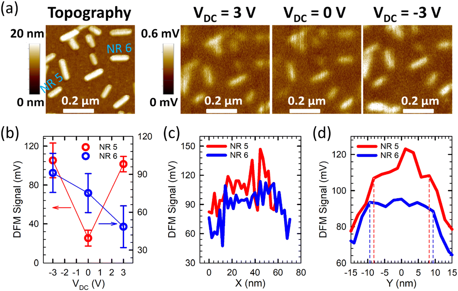 | ||
| Fig. 4 (a) Topographical image and dielectric response images of an area with multiple well-separated CsPbBr3 nanorods, including NR 5 (diameter 10 ± 1 nm) and NR 6 (diameter 11 ± 1 nm), 62 days after the sample was synthesized. (b) DFM signal as a function of VDC for NR 5 and NR 6. (c) DFM signal as a function of X extracted from the dielectric response images for NR 5 and NR 6 at VDC = –3 V. (d) DFM signal as a function of Y extracted from the dielectric response images for NR 5 and NR 6 at VDC = –3 V, where the boundaries of the Y-range with nearly constant DFM signals are indicated by dashed lines. | ||
Although the ambipolar to p-type transition did not occur exactly the same day for all NRs, nearly all NRs completed the transition within two weeks. Fig. 5a shows topography and DFM images of a 0.5 μm × 0.5 μm area with multiple NRs. The measurement was conducted 74 days after sample synthesis. All NRs displayed the strongest DFM response at VDC = –3 V and the weakest DFM response at VDC = 3 V, signifying p-type behaviors. Quantitative DFM signals were also extracted for two representative NRs, labeled NR 7 and NR 8. Fig. 5b shows their DFM signals as a function of VDC, confirming the completion of their transition to p-type NRs. Even after the ambipolar to p-type transition, the NRs maintained well-defined morphology without any sign of degradation, as evident from the topographical image. Moreover, longitudinal and transverse dielectric response profiles, as shown in Fig. 5c and d for NR 7 and NR 8 at VDC = 3 V, as examples, unveiled reasonably good nanoscale electronic homogeneity despite the transition of their polarity from ambipolar to unipolar p-type. The relative standard deviations of the dielectric response profiles in the longitudinal direction were 9.2% and 6.7%, and in the transverse direction were 1.7% and 5.7%, for NR 7 and NR 8, respectively.
 | ||
| Fig. 5 (a) Topographical image and dielectric response images of an area with multiple well-separated CsPbBr3 nanorods, including NR 7 (diameter: 12 ± 1 nm) and NR 8 (diameter 10 ± 1 nm), 74 days after the sample was synthesized. (b) DFM signal as a function of VDC for NR 7 and NR 8. (c) DFM signal as a function of X extracted from the dielectric response images for NR 7 and NR 8 at VDC = 3 V. (d) DFM signal as a function of Y extracted from the dielectric response images for NR 7 and NR 8 at VDC = 3 V, where the boundaries of the Y-range with nearly constant DFM signals are indicated by dashed lines. | ||
The transition to p-type could be induced by the presence of oxygen in the air. In a recent study, Shin et al. achieved reversible diffusion of oxygen into MAPbI3 thin films, and their photoemission experiments revealed that oxygen diffusion led to pronounced p-doping in MAPbI3 which was attributed to oxygen substitution of iodine vacancies.35 Similar oxygen substitution of bromide vacancies could occur in template-grown CsPbBr3 NRs, after allowing sufficient time for oxygen to diffuse into PS-ligated CsPbBr3 NRs. Indeed, the degradation of PS-ligated PbSe nanoparticles (NPs), induced by oxygen/moisture diffusion, has been reported.36 The underlying mechanism for the ambipolar to p-type transition in template-grown CsPbBr3 NRs deserves a thorough investigation, which could potentially lead to controllable electronic doping and highly desirable uniform p-type CsPbBr3 nanocrystals.37
4 Conclusions
In summary, we synthesized perovskite CsPbBr3 NRs using amphiphilic bottlebrush-like block copolymer as nanoreactors and performed contactless DFM characterizations on the as-synthesized NRs to study their electronic properties. We found that all template-grown CsPbBr3 NRs exhibited ambipolar behaviors within two months of sample synthesis. A transition from ambipolar to p-type behaviors occurred afterwards and within a transition window of about two weeks, nearly all NRs completed the transition to p-type. Moreover, our experiments revealed good longitudinal and transverse nanoscale electronic homogeneity in the template-grown CsPbBr3 NRs before and after the transition. The remarkable improvement of the electronic uniformity and nanoscale homogeneity in templated CsPbBr3 NRs, over conventional CsPbBr3 NWs, opens a new avenue of device applications utilizing one-dimensional perovskite nanocrystals with uniform electronic properties and minimum defects.Conflicts of interest
There are no conflicts to declare.Acknowledgements
This work was supported by the National Science Foundation through grants DMR-1904042 and DMR-1903990.References
- S. Kazim, M. K. Nazeeruddin, M. Grätzel and S. Ahmad, Angew. Chem., Int. Ed., 2014, 53, 2812–2824 CrossRef CAS PubMed.
- S. D. Stranks and H. J. Snaith, Nat. Nanotechnol., 2015, 10, 391–402 CrossRef CAS PubMed.
- D. Zhang, Y. Yang, Y. Bekenstein, Y. Yu, N. A. Gibson, A. B. Wong, S. W. Eaton, N. Kornienko, Q. Kong, M. Lai, A. P. Alivisatos, S. R. Leone and P. Yang, J. Am. Chem. Soc., 2016, 138, 7236–7239 CrossRef CAS PubMed.
- J. Kang and L. W. Wang, J. Phys. Chem. Lett., 2017, 8, 489–493 CrossRef CAS PubMed.
- E. Oksenberg, E. Sanders, R. Popovitz-Biro, L. Houben and E. Joselevich, Nano Lett., 2018, 18, 424–433 CrossRef CAS PubMed.
- Q. Zhang and Y. Yin, ACS Cent. Sci., 2018, 4, 668–679 CrossRef CAS PubMed.
- T. Ma, S. Wang, Y. Zhang, K. Zhang and L. Yi, J. Mater. Sci., 2020, 55, 464–479 CrossRef CAS.
- A. B. Wong, M. Lai, S. W. Eaton, Y. Yu, E. Lin, L. Dou, A. Fu and P. Yang, Nano Lett., 2015, 15, 5519–5524 CrossRef CAS PubMed.
- D. Zhang, Y. Yu, Y. Bekenstein, A. B. Wong, A. P. Alivisatos and P. Yang, J. Am. Chem. Soc., 2016, 138, 13155–13158 CrossRef CAS PubMed.
- J. Deng, J. Li, Z. Yang and M. Wang, J. Mater. Chem. C, 2019, 7, 12415–12440 RSC.
- S. W. Eaton, M. Lai, N. A. Gibson, A. B. Wong, L. Dou, J. Ma, L. W. Wang, S. R. Leone and P. Yang, Proc. Natl. Acad. Sci. U. S. A., 2016, 113, 1993–1998 CrossRef CAS PubMed.
- G. Xu, Y. Li, J. Yan, X. Lv, Y. Liu and B. Cai, Mater. Res. Lett., 2019, 7, 203–209 CrossRef CAS.
- J. Shamsi, A. S. Urban, M. Imran, L. De Trizio and L. Manna, Chem. Rev., 2019, 119, 3296–3348 CrossRef CAS PubMed.
- A. Pan, B. He, X. Fan, Z. Liu, J. J. Urban, A. P. Alivisatos, L. He and Y. Liu, ACS Nano, 2016, 10, 7943–7954 CrossRef CAS PubMed.
- J. Shamsi, P. Rastogi, V. Caligiuri, A. L. Abdelhady, D. Spirito, L. Manna and R. Krahne, ACS Nano, 2017, 11, 10206–10213 CrossRef CAS PubMed.
- J. Shamsi, Z. Dang, P. Bianchini, C. Canale, F. Di Stasio, R. Brescia, M. Prato and L. Manna, J. Am. Chem. Soc., 2016, 138, 7240–7243 CrossRef CAS PubMed.
- M. Gao, H. Liu, S. Yu, S. Louisia, Y. Zhang, D. P. Nenon, A. P. Alivisatos and P. Yang, J. Am. Chem. Soc., 2020, 142, 8871–8879 CrossRef PubMed.
- D. Zhang, S. W. Eaton, Y. Yu, D. Dou and P. Yang, J. Am. Chem. Soc., 2015, 137, 9230–9233 CrossRef CAS PubMed.
- Y. Dou, F. Cao, T. Dudka, Y. Li, S. Wang, C. Zhang, Y. Gao, X. Yang and A. L. Rogach, ACS Mater. Lett., 2020, 2, 814–820 CrossRef CAS.
- Y. Li, H. Huang, Y. Xiong, A. F. Richter, S. V. Kershaw, J. Feldmann and A. L. Rogach, ACS Nano, 2019, 13, 8237–8245 CrossRef CAS PubMed.
- J. Li, Q. Jing, S. Xiao, Y. Gao, Y. Wang, W. Zhang, X. W. Sun, K. Wang and T. He, J. Phys. Chem. Lett., 2020, 11, 4817–4825 CrossRef CAS PubMed.
- D. Yang, P. Li, Y. Zou, M. Cao, H. Hu, Q. Zhong, J. Hu, B. Sun, S. Duhm and Y. Xu, Chem. Mater., 2019, 31, 1575–1583 CrossRef CAS.
- Q. Li, Y. Yang, W. Que and T. Lian, Nano Lett., 2019, 19, 5620–5627 CrossRef CAS PubMed.
- M. Imran, F. Di Stasio, Z. Dang, C. Canale, A. H. Khan, J. Shamsi, R. Brescia, M. Prato and L. Manna, Chem. Mater., 2016, 28, 6450–6454 CrossRef CAS PubMed.
- J. He, A. Towers, Y. Wang, P. Yuan, Z. Jiang, J. Chen, A. J. Gesquiere, S. T. Wu and Y. Dong, Nanoscale, 2018, 10, 15436–15441 RSC.
- H. Zhou, S. Yuan, X. Wang, T. Xu, X. Wang, H. Li, W. Zheng, P. Fan, Y. Li and L. Sun, ACS Nano, 2017, 11, 1189–1195 CrossRef CAS PubMed.
- Y. S. Li, S. Liang, T. Trieu, R. R. Bautista and Z. Lin, ACS Appl. Energy Mater., 2022, 5, 4431–4438 CrossRef CAS.
- S. Liang, M. Zhang, S. He, M. Tian, W. Choi, T. Lian and Z. Lin, Nat. Synth., 2023, 2, 719–728 CrossRef.
- Y. Meng, C. Lan, F. Li, S. Yip, R. Wei, X. Kang, X. Bu, R. Dong, H. Zhang and J. C. Ho, ACS Nano, 2019, 13, 6060–6070 CrossRef CAS PubMed.
- Y. Meng, Z. Lai, F. Li, W. Wang, S. Yip, Q. Quan, X. Bu, F. Wang, Y. Bao, T. Hosomi, T. Takahashi, K. Nagashima, T. Yanagida, J. Lu and J. Ho, ACS Nano, 2020, 14, 12749–12760 CrossRef CAS PubMed.
- Y. S. Li, J. Ge, J. Cai, J. Zhang, W. Lu, J. Liu and L. Chen, Nano Res., 2014, 7, 1623–1630 CrossRef CAS.
- W. Lu, J. Zhang, Y. S. Li, Q. Chen, X. Wang, A. Hassanien and L. Chen, J. Phys. Chem. C, 2012, 116, 7158–7163 CrossRef CAS.
- J. Zhang, W. Lu, Y. S. Li, D. Lu, T. Zhang, X. Wang and L. Chen, Acc. Chem. Res., 2015, 48, 1788–1796 CrossRef CAS PubMed.
- T. Stabile and Y. S. Li, Mater. Today Adv., 2021, 12, 100189 CrossRef CAS.
- D. Shin, F. Zu, A. V. Cohen, Y. Yi, L. Kronik and N. Koch, Adv. Mater., 2021, 33, 2100211 CrossRef CAS PubMed.
- S. Liang, M. Zhang, Y. He, Z. Kang, M. Tian, M. Zhang, H. Miao and Z. Lin, Chem. Mater., 2021, 33, 6701–6712 CrossRef CAS.
- J. T. Mulder, I. du Fossé, M. A. Jazi, L. Mann and A. J. Houtepen, ACS Energy Lett., 2021, 6, 2519–2525 CrossRef CAS PubMed.
Footnote |
| † Electronic supplementary information (ESI) available. See DOI: https://doi.org/10.1039/d3nr06682g |
| This journal is © The Royal Society of Chemistry 2024 |