
 Open Access Article
 This Open Access Article is licensed under a
 Creative Commons Attribution 3.0 Unported Licence
Photosensitised silicon solar cells: progress and challenges
Lefteris Danos
 *a,
Liping Fang
*b,
Branislav Dzurňak
c,
Pattareeya Damrongsak
d,
Dieter Meissner
e and
Tom Markvart
cf
*a,
Liping Fang
*b,
Branislav Dzurňak
c,
Pattareeya Damrongsak
d,
Dieter Meissner
e and
Tom Markvart
cf
aDepartment of Chemistry, Energy Lancaster, Lancaster University, Lancaster, LA1 4YB, UK. E-mail: l.danos@lancaster.ac.uk
bGuangdong Laboratory of Machine Perception and Intelligent Computing, and Faculty of Engineering, Shenzhen MSU-BIT University, Shenzhen, 518172, China. E-mail: liping.fang@smbu.edu.cn
cCentre for Advanced Photovoltaics, Faculty of Electrical Engineering, Czech Technical University in Prague, Prague, 16627, Czech Republic
dDepartment of Physics, School of Science, King Mongkut's Institute of Technology Ladkrabang, Bangkok, 10520, Thailand
eLIOS, Johannes Keppler Univ. Linz, Altenberger Str. 69, 4040 Linz, Austria
fSolar Energy Laboratory, Faculty of Engineering and Physical Sciences, University of Southampton, Southampton, SO17 1BJ, UK
First published on 2nd July 2025
Abstract
We present historical context and review recent advances in the realisation of a photosensitised silicon solar cell, highlighting key theoretical and experimental developments. Emphasis is placed on the importance of electrostatic near-field interaction between the transition dipole moments of the luminophore and electron–hole pairs in the silicon crystal at a distance of a few nanometres. The very fast energy transfer then resembles the Förster resonance energy transfer between two molecules. Photon tunnelling via the evanescent field of the excited molecule (‘optical near field’) into optical states in silicon occurs at somewhat larger separation between the molecule and silicon, of the order of tens of nanometres. Accessing the critical Förster regime relies on oxide-free silicon surfaces and the covalent attachment of dyes, enabling efficient passivation and precise control of interface chemistry. Realising a complete photosensitised silicon solar cell remains a challenge and we outline promising directions and review recent progress that brings this goal closer to reality.
 Lefteris Danos | Lefteris Danos is a Lecturer at the Department of Chemistry at Lancaster University. He received his MChem degree from the University of Leeds and completed his PhD in Chemistry at the University of Southampton, specialising in spectroscopy. He subsequently joined Professor Markvart's Solar Energy Laboratory at Southampton as a postdoctoral research fellow. After a short appointment at the Department of Materials at Imperial College London, he moved to Lancaster University to support the establishment of the new Chemistry Department. His research focuses on the development of light-harvesting structures for photovoltaic applications. |
 Liping Fang | Dr Liping Fang serves as a Senior Lecturer at Shenzhen MSU-BIT University. He earned his PhD in Photonics for Photovoltaics from the University of Southampton under the guidance of Professor Tom Markvart. Prior to his doctoral studies, he received both his BSc in Optical Information Engineering and MSc in Physical Electronics from the Beijing Institute of Technology. His research focuses on areas including nanophotonics, photovoltaics, energy transfer, thin films, and ellipsometry. |
 Branislav Dzurňak | Branislav Dzurnak is an assistant professor at Faculty of Electrical Engineering, Czech Technical University in Prague. He holds a PhD degree in quantum optics and optoelectronics from Charles University where he focused on time-resolved spectroscopy of nanomaterials. His further research explored quantum phenomena such as quantum key distribution at Toshiba Europe Ltd and polariton formation at University of Sheffield, where he continued his research on time-resolved spectroscopy investigating organic materials for photovoltaic applications. His current research interests include light-harvesting structures and sensitization mechanisms for novel photovoltaic devices. |
 Pattareeya Damrongsak | Assoc. Prof. Pattareeya Damrongsak is the Head of the Physics Department and a lecturer at King Mongkut's Institute of Technology Ladkrabang, Thailand. She earned her PhD in Engineering Materials from the University of Southampton in 2007 and brings extensive experience in teaching, research, and curriculum development. Her professional interests include supporting student development and conducting research, particularly on fluorescent materials for photovoltaic applications. Additionally, she specializes in experimental techniques and the development of learning apparatus for physics education. |
 Dieter Meissner | Dieter Meissner is a retired Univ.-Prof. (Tallinn Univ. of Technology, JKU Linz, Osaka Univ., Univ. Buenos Aires), with a PhD in Physical Chemistry from the Univ. of Hamburg, Germany, and a Dr.h.c. from TUT. He developed BSc and MSc curricula in Sustainable Energetics. His research started with solar (PEC) water splitting and all types of non-silicon photovoltaics as well as fuel cells. He founded a few spin-out companies, of which Crystalsol developed a unique powder-based low-cost semiconductor and PV module production. He has published more than 200 scientific papers and filed more than 150 patents. |
 Tom Markvart | Tom Markvart is with the Centre for Advanced Photovoltaics at the Czech Technical University in Prague and an Emeritus Professor of Energy Conversion at the University of Southampton, UK. His research and education work in photovoltaics includes projects on the radiation resistant solar cells with the European Space Agency, solar vaccine refrigeration for the World Health Organisation, and the textbook “Solar Electricity” for the UNESCO Energy Engineering Programme. He was a Rapporteur for the Working Group Photovoltaics within the SET Plan of the European Commission. Tom's current research focuses on future generation of solar cells and the thermodynamics of light. |
Introduction
Crystalline silicon (Si) solar cells dominate the photovoltaics (PV) market with more than 95% installed modules worldwide1 and an installed global capacity over 2 TW.2 Nevertheless, achieving complete elimination of CO2 emissions worldwide by replacing all fossil fuel-based energy systems would require the installed PV capacity to increase by nearly two orders of magnitude.3 Achieving such a feat will require the implementation of manufacturing processes that consume less energy.The industrial production of silicon for both microelectronics and photovoltaic technologies remains an energy intensive and carbon emitting process. From the high temperature quartz reduction to the purification of polysilicon and crystal growth, each step demands substantial electricity, which is often derived from fossil fuels and results in significant CO2 emissions.4
PV recycling methods that can recover silicon wafers, precious metals, aluminium and glass already exist but issues still remain with implementation such as the absence of policy in some parts of the word, not being economically viable yet, and facing environmental concerns for some of the material retrieving processes.5,6 Therefore, many new approaches that use less silicon are currently tested towards a sustainable development in an increasing number of research labs.
Silicon being an indirect bandgap semiconductor is not a good light absorber, and the current manufacturing processes for thick wafers (∼150 μm) are energy intensive. In this feature article we present historical developments and current challenges towards the realisation of a photosensitised crystalline Si solar cell. The photosensitisation of an indirect semiconductor such as Si can offer a paradigm shift in the fabrication of sustainable solar cells. The photosensitisation process involves the transfer of excited state energy from chromophores near the surface of Si (∼5 nm), resulting in the generation of electron–hole pairs. It was first proposed by Dexter7 and holds the potential to reduce the amount of Si currently used in PV cells by up to two orders of magnitude.
A dipole–dipole near field interaction has similarities to the photophysical process of light harvesting occurring in photosynthesis via the antenna pigments surrounding the reaction centre (Fig. 1).8–10 The light harvesting complex transfers the absorbed energy non-radiatively with over 95% efficiency to the reaction centre where the onset of electron transfer occurs. The whole process results in enhancing the absorption coefficient of the reaction centre by orders of magnitude.
 | ||
| Fig. 1 Crystal structure of the LH1-RC complex from Thermochromatium tepidum in C2 form8 obtained from PDB (3WMM).9,10 | ||
The proposed photosensitisation applied to solar cells results in splitting of the PV process into two separate steps. An energy collector (Step 1) absorbs light with high efficiency similar to the light harvesting antenna in photosynthesis and transfers the energy via exciton diffusion to an ultra-thin Si converter (Step 2), which efficiently separates the photo-generated charges akin to the reaction centre in photosynthesis. Furthermore, the photosensitisation of Si can be augmented via recent attempts to overcome the single junction efficiency limit with photophysical processes such as singlet fission11–13 and triplet–triplet annihilation.14,15
In this paper, we first provide a brief historical overview of the development of sensitisation, followed by an outline of the theoretical framework governing energy transfer between dye molecules and dye–semiconductor systems. We identify two distinct mechanisms of non-radiative energy transfer: Förster resonance energy transfer (FRET) at short distances (<10 nm) and photon tunnelling at intermediate distances (15–100 nm). In the section on luminescence quenching at Si surfaces, we review experimental evidence for the photosensitisation of silicon, highlighting key luminescence quenching studies involving dyes and quantum dots on the Si surface. The section on engineering the dye–Si interface presents results about oxide-free Si surfaces and the direct covalent attachment of dyes to the Si surface. This approach enables access to dye–Si distances less than 1.5 nm. We then begin to outline the key requirements for the development of a photosensitised solar cell. We conclude by discussing the future potential and the challenges that must be addressed to achieve the realisation of such a device.
Historical development of sensitisation
William Henry Fox Talbot16 used the term sensitisation in his discovery of the photographic process. He developed a light sensitive paper containing silver iodide via a chemical method, which later was referred to as sensitised paper. Luis Daguerre17 developed a similar process using copper plates coated with silver iodide. Silver was deposited onto copper plates and oxidised (‘sensitised’) exposing it to iodine vapour. Both researchers made use of chemical sensitisation of silver to form halides, making them light sensitive. In the same period Edmond Becquerel18,19 was the first to demonstrate the photovoltaic effect by observing a photocurrent in illuminated Pt electrodes covered with silver halide immersed in an acidic aqueous solution.The term sensitisation came to describe a process by which the photosensitivity of a solid material is extended to a wavelength region that the solid does not directly absorb light and therefore is not sensitive to light excitation. Subsequent researchers tested many organic dyes that allowed the extension of the sensitivity of silver halides further to the red and infra-red region of the electromagnetic spectrum.20 During the same period, spectral sensitisation using various organic dyes was also applied to wide band gap semiconductors such as copper oxide by H. Rigollot21,22 in order to extend the optical sensitivity of the semiconductor beyond their band gap energy.
Nowadays the term sensitisation is also associated with light harvesting occurring in natural photosynthesis. In 1932, Robert Emerson and William Arnold studied the photosynthesis of green algae23 with short pulses of light and discovered that a large number of chlorophylls (2480) are present per carbon dioxide reduced. This unexpectedly high ratio led to the proposal by Gaffron and Wohl24 that most chlorophyll molecules do not participate in carbon reduction but instead function as light harvesting antenna that transfer the energy to a small number, which makes up the reaction centre, and electron transfer occurs.25
Detailed investigation of the photographic sensitisation during the 1930s pointed towards an energy transfer from monomolecular adsorbates of excited organic dyes to the silver halide crystals.26–29
In 1948, Theodore Förster proposed his theory of resonance energy transfer30 between molecules and it was soon used to explain the function and photophysical mechanism of non-radiative energy transfer in light harvesting antenna in photosynthesis. By the late 60s and early 70s a complete picture of the function of light harvesting antenna emerged in photosynthesis based on FRET explaining the observed energy migration.
Research into sensitisation of semiconductors begun with a series of experiments in the 60s with dyes adsorbed on wide band gap semiconductors such as TiO2, SnO2, ZnO, and SiC. Experiments monitoring the photocurrent as a function of incident light wavelength were carried out for potential applications in photoelectrochemical solar energy conversion and storage.31 The proposed sensitisation mechanism, which sparked a scientific debate, was suggested to involve either electron transfer or energy transfer. In the energy transfer mechanism, the excited dye molecules can either transfer their energy to discharge surface traps (wide band gap semiconductors) or excite electron–hole pairs (narrow band gap semiconductors).32,33 Pre-1980, sensitisation work in the Soviet Union was summarised by Akimov, Cherkasov and Cherkashin34,35 who, in addition to spectral sensitisation (appearance of new light-sensitive bands), introduced also chemical and structural sensitisation. In contrast, the proposed electron transfer mechanism involves the direct injection of electrons from the excited state of the dye into the semiconductor's conduction band. This interpretation became dominant in photoelectrochemistry.36–39
With the advent of silicon photovoltaics after the oil crisis a renewed focus developed for the spectral sensitisation of Si. In 1979, Dexter proposed a novel idea,7 the production of electron–hole (e–h) pairs in a semiconductor via non-radiative energy transfer from dye molecules on the surface of the semiconductor. In his introduction Dexter mentions that a similar mechanism is presumed to occur in the sensitisation of silver halides from exciton energy transfer to traps producing free electrons.
His proposal suggested the creation of triplet excitons from excited dye molecules on the surface of a semiconductor generated via inter-system crossing or singlet fission.
The triplet excitons may diffuse to the surface of the semiconductor and transfer their excitation energy to surface traps which will then produce e–h pairs. This operation can even work in indirect semiconductors and reduce the amount of expensive semiconductor. He postulated that the necessary momentum conservation is bypassed by the surface molecule via recoil.
Since then, several researchers have studied the mechanism of silicon photosensitisation and concluded that it occurs via energy transfer akin to FRET. Most work, since Dexter's original proposal, focused on luminescence quenching as a function of the distance of chromophores on the surface of Si providing evidence of FRET and potential electron–hole generation.
Theoretical foundations
Förster theory
Energy transfer mediated by the electromagnetic field – as opposed to collisions – was first observed between excited atoms in the gas phase in the early part of the 20th century by Franck and Cario.40 A similar explanation was used to explain the fluorescence depolarization of molecules in solution and for the fluorescence quenching of anthracene crystals by naphthalene impurities. In 1932, Emerson and Arnold's discovery23 that the primary chemical reaction in photosynthesis is sensitised by the absorption of a light quantum by several hundred chlorophyll molecules was subsequently explained in terms of energy transfer between pigment molecules in the photosynthetic unit by Gaffron and Wohl.24The first theories proposed by Jean and Francis Perrin41,42 predicted a transfer distance by an order of magnitude larger than observed.
A satisfactory account had to await the Förster paper published in 1948,30 who explained the energy transfer in terms of near-field electrostatic interaction between the transition dipole moments on the molecules. Förster's theory of resonance energy transfer was subsequently generalised by Dexter to multipole transitions,43 transitions induced by the exchange interaction and was later interpreted as thermally activated hopping of the excitonic polaron.
FRET resembles radiative transfer (reabsorption by another molecule) but that occurs for molecules at close separation. Interaction between two molecules, a donor and an acceptor (represented as absorbing/emitting dipoles), occurs within the far field (radiative zone) where the electric field at distance R from the emitting dipole is proportional to Eff ∼ λ/2πR, where λ is the emission wavelength. The radiative transfer rate per unit wavelength interval can be cast in the form of dkrt/dλ = F(λ)σabs(λ)/4πR2τf, where F(λ) is the fluorescence lineshape function normalised to unity on the wavelength scale, σabs(λ) is the absorption cross section, and τf is the fluorescence lifetime.
Förster transfer is a nonradiative process with no exchange of photons, analogous to the radiative transfer but occurring in the near field where the electric field is proportional to Enf ∼ (λ/2πR)3. Quantum mechanics gives the transition rate proportional to the square of the interaction energy, which, in turn, is proportional to the electric field. Transferring the molecules from the far field into the near field to obtain the Förster transfer rate therefore means scaling the radiative rate by the factor kF = |Enf/Eff|2krt = (λ/R)4, and one can readily obtain the Förster transfer rate using the following equation (Fig. 2a):
 | (1) |
![[small tau, Greek, macron]](https://www.rsc.org/images/entities/i_char_e0d4.gif) f is the actual (measured) fluorescence lifetime and
f is the actual (measured) fluorescence lifetime and ![[R with combining macron]](https://www.rsc.org/images/entities/i_char_0052_0304.gif) o is the Förster transfer radius when the transfer rate is equal to the fluorescence rate:
o is the Förster transfer radius when the transfer rate is equal to the fluorescence rate:
 | (2) |
 | ||
| Fig. 2 (a) Schematic illustration of Förster resonance energy transfer (FRET) between a donor and an acceptor molecule. The donor molecule (left) is initially excited by absorbing a photon (hν), reaching an electronically excited state. If the donor and acceptor are in close proximity (typically 1–10 nm), and their emission and absorption spectra overlap, energy can be non-radiatively transferred from the donor to the acceptor via dipole–dipole coupling. (b) Schematic of the energy transfer mechanisms that can enhance the optical excitation of crystalline Si using nearby luminescent molecules. Here, a donor molecule absorbs incident light, which subsequently couples its energy to the electronic states of Si. (c) Schematic highlighting the possibility of non-phonon-assisted electronic transitions in Si due to the strong coupling between the excited state of the donor molecule and the electronic states of c-Si. In conventional absorption, indirect transitions in Si require phonon participation to conserve momentum. Here, the diagram proposes a direct transfer mechanism where the excitation energy from the donor may drive a transition across the Si bandgap without phonon assistance (highlighted in red). | ||
Eqn (2) can be simplified by using a Marcus-like model for the broadening of spectral lines by the interaction with the solvent molecules.
The absorption and fluorescent lines then take the Gaussian shape of width 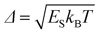 , where ES is the Stokes shift in energy units, T is the temperature and kB is the Boltzmann constant.
The Förster radius then takes the particularly simple form
 | (3) |
The Förster theory predicts the excitation transfer rate proportional to the inverse sixth power of the distance between the donor and acceptor, with a characteristic radius equal to λo/2πn multiplied, for a unit quantum yield, by the sixth root of the ratio of the product of maximum absorption cross-section and the emission wavelength in the medium. For good absorbers, the absorption cross-section σo is on the order of several Å2. We then find that, for wavelengths in the visible part of the spectrum, the Förster radius comes out on the order of several nanometres. This paper is about resonance energy transfer from the molecule to the semiconductor where our understanding is much more limited (Fig. 2b).
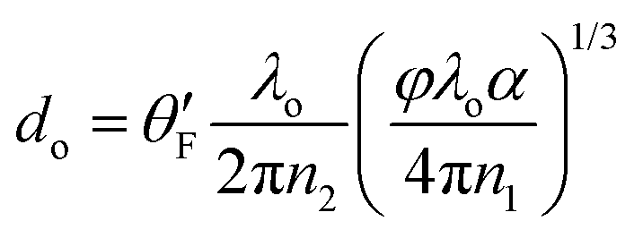
To our knowledge, the only theoretical result for the transfer rate was obtained by Chance Prock and Silbey (CPS),44 which can be cast in the approximate form
 | (4) |
 | (5) |
 is an orientational factor equal to (3/4)1/3, (1/4)1/3 and (1/2)1/3 for perpendicular, parallel and isotropic orientation.
CPS theory therefore predicts the energy transfer rate proportional to the inverse cube of the distance of the molecule from the semiconductor – a result that can also be obtained by representing the semiconductor as a collection of transition dipole moments filling a semi-infinite half space. The characteristic separation between the molecule and the semiconductor is now again proportional to λo/2πn, now multiplied by the product of the absorption coefficient and emission wavelength in the spacer medium. For the energy transfer between a molecule and semiconductor, the values of do predicted by CPS theory are typically several nanometers, similar to the Förster radius between two molecules. The available experimental data will be discussed in the Luminescence quenching at Si surfaces section. More experimental evidence is available for metals where do is roughly an order of magnitude larger.
The question, however, arises whether the use of the absorption is appropriate, particularly for indirect-gap semiconductors such as silicon. The absorption coefficient describes the absorption of photons with a definite wavevector or photon momentum. Wavevector conservation imposes severe constraints on the absorption process, necessitating the participation of phonons, which reduces substantially the absorption coefficient. Resonance energy transfer, in contrast, occurs from a localised electron state, without a definite wavenumber. Without the constraints of wavevector conservation, can silicon be expected to behave as direct-bandgap semiconductor (Fig. 2c)?
A short note on Chance, Prock and Silbey (CPS) theory
The modification of molecular fluorescence near metal surfaces is a well-studied phenomenon, with seminal contributions from Drexhage,45 Kuhn,46,47 and Chance, Prock, and Silbey (CPS).44 Drexhage experimentally measured the fluorescence lifetimes of Eu3+ ions in Langmuir–Blodgett (LB) monolayers placed at various distances from gold, silver, and copper mirrors.45 These results were successfully modelled by the classical electromagnetic theory developed by CPS, which treats the molecule as an oscillating electric dipole and describes the metal via its dielectric constant.44The CPS theory originates from Kuhn's earlier model,46 where a classical harmonic oscillator (representing the molecular dipole) interacts with its own electromagnetic field reflected by the proximal mirror. Calculating these reflected fields requires solving Maxwell's equations subject to the system's boundary conditions. Incorporating the reflected fields into Kuhn's oscillator model allows for the determination of the modified fluorescence decay rates near the metal surface.
Later work demonstrated that the CPS theory can be reproduced using Fermi's Golden Rule48 by incorporating the concept of the local density of states (LDOS) of the electromagnetic modes.49 It is noteworthy that the principle of tuning spontaneous emission properties by modifying the surrounding LDOS was first elucidated by Purcell over half a century ago, albeit in the context of radio frequency electromagnetic waves.50
Photon tunnelling theory
At a molecule–Si distance larger than 10 nanometres, the dominant energy transfer mechanism is based on a parallel – optical – mechanism where energy is injected via the evanescent field into a manifold of states in the solar cell (Fig. 3), which are forbidden from direct excitation by Snell's law.51,52 We call this type of energy transfer photon tunnelling.53–55 As the injected light then travels along the solar cell it has a much higher chance of being absorbed and excites electron–hole pairs.56 Photon tunnelling can thus be considered as a technique for light trapping in Si solar cells. A detailed balance treatment of light trapping in thin films is given in ref. 57, which showed that significant enhancements in absorption are possible even when the thin Si film only supports a limited number of waveguide modes. | ||
| Fig. 3 (a) Light refraction near a thin silicon waveguide where the forbidden modes are inaccessible. (b) Photon tunnelling from excited fluorescent molecules to the forbidden states in the silicon thin film. (c) The dependence of power dissipated in the three distinct channels on the dipole-silicon separation (the dependence of light harvesting can be fitted by the inverse cubic law, whereas the photon tunnelling rate shows a linear dependence on dipole-Si separation since the 25-nm-thick Si film only supports a single waveguide mode). (d) The probability of energy transfer to a 25-nm-thick silicon film (dashed line) or bulk silicon (full line) via light harvesting or photon tunnelling, compared with photon loss by fluorescence emitted in the far field. The probabilities of both photon tunnelling and light harvesting to excite electron–hole pairs in a thin silicon structure is high and highlights the substantial potential for photovoltaics applications. Reproduced from ref. 53 with permission from IEEE. Copyright 2014. | ||
The photon tunnelling rate to a thin silicon solar cell, perceiving as a waveguide,56 can be obtained either by a pure quantum mechanical approach involving counting the density of optical states in the thin Si waveguide54 or a complex variable analysis in the in-plane wavenumber plane.55 For tunnelling to an ultrathin silicon cell which only supports a single waveguide mode, the tunnelling rate is simply an exponential function (Fig. 3c):
| bpt = C·exp(−2γd) | (6) |
The photon tunnelling rate to a bulk silicon solar cell has a similar form to that for the previously discussed thick silicon cell, but now the summation over discrete modes is replaced by an integral over the continuous manifold of the aforementioned forbidden states in bulk silicon. The resultant tunnelling rate is given by an integral of the tunnelling constant in the form of:
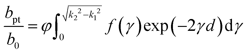 | (7) |
The energy transfer probability or efficiency from the excited molecule to silicon can be calculated by dividing the summation of the photon tunnelling rate and the energy transfer rate via FRET into the total power dissipation rate:
 | (8) |
The energy transfer rates and probabilities of power dissipation of dipole radiation into the three channels (far field fluorescence; tunnelling into waveguide modes and light harvesting) are compared in Fig. 3(c and d). It is depicted in Fig. 3c that the dominant energy transfer process is via light harvesting when the dipole–Si distance is only a few nanometres. In the intermediate distance range (several hundreds of nanometres), photon tunnelling dominates the energy transfer process. At even larger separations, the fluctuation of the damping rate is due to the interference of the source wave of the molecular dipole and its reflected wave from the Si surface. Fig. 3d clearly indicates that the probabilities of both photon tunnelling and light harvesting to excite electron–hole pairs in a thin silicon structure is as high as a thick silicon wafer and highlights the substantial potential for photovoltaic applications. Further work is required, however, to expand the theoretical landscape and include reverse transitions, particularly the effect on the tunnelling efficiency. The challenge, in effect, is to expand the thermodynamic treatment to the nanoscale.53
Luminescence quenching at Si surfaces
In this section we present experiments using dye molecules or quantum dots (QDs) for the sensitisation (via energy transfer) of Si. We focus on luminescence quenching observed near the surface of Si as evidence of FRET or photon tunnelling from the donor (dye/QD) chromophore to the Si substrate. The unquenched lifetime is typically measured from a dye/QD monolayer deposited either on quartz substrates or on thick spacer layers grown on silicon.Dye monolayers on the surface of Si
The theoretical framework developed by Chance Prock and Silbey (CPS) in the late 70s for excited states of dyes near the surface of metals was soon extended to semiconductors. The luminescence distance dependence in the quenching region (1–10 nm) was expected to show d−3 distance dependence for non-radiative energy transfer to the bulk of the semiconductor.44,46Initial experiments carried out from Hayashi et al.58 on evaporated tetracene films deposited on GaAs or Si substrates revealed the expected oscillations in the far-field region at large dye–semiconductor distances but the measured non-radiative decay rate deviated from a d−3 distance dependence in the quenching regime at less than 4 nm separation from the semiconductor surface and instead an exponential model was proposed. A possible reason for this deviation is that the decay rates were inferred from fluorescence intensity measurements which are known to be prone to significant radiation pattern changes and therefore decay lifetimes are preferred instead.
A study conducted by Whitmore et al.59 on pyrazine decay data on GaAs as a function of distance using ammonia as a spacer layer showed the classical predicated d−3 dependence in the quenching region. Alivisatos et al.60 studied the decay lifetimes of pyrene evaporated layers on silicon with Xe used as a spacer and found the expected quenching of the lifetimes as the donor–Si distance is reduced although intralayer pyrene–pyrene energy transfer was also present. Plotnikov et al.61 studied the aggregation effects of Rhodamine B dyes adsorbed on silicon and germanium substrates with a small thickness (3–30 nm) of oxide present and measured fluorescence decays as a function of distance to the semiconductor (Si or Ge).
Elegant experiments using Langmuir–Blodgett (LB) films also demonstrated luminescence quenching as a function of distance to metal surfaces45,62 and soon were extended to semiconductors. A study conducted by Sluch et al.63 investigated the emission lifetime shortening of LB mixed monolayers of palmitic acid with tricosanoic acid as a function of distance to the Si surface and showed a d−3 dependence for distances between 10 and 30 nm but showed a deviation (slower rate dependence) for distances between 2.5 and 5 nm.
By the late 90s a picture of the complexity of the subject started to emerge. The results of all the different luminescence quenching studies revealed that there were several parameters that needed to be taken into account such as the effect of dye concentration on the monolayer,61 intralayer energy transfer60 or aggregate formation,64 the effect of semiconductor doping density,65 the presence of charging states on the surface,37 the insulator spacer,66 temperature effects and other factors.
In the early 2000s, research on PV began to gain momentum, with various novel concepts being explored. The concept of light harvesting was proposed for quantum solar energy conversion creating a strong link between Si solar cells and photosynthesis.67 This followed on the earlier discovery of dye sensitised solar cells68 where dyes adsorbed on nanocrystalline titanium oxide sensitised the wide band gap TiO2 via electron transfer. Regeneration of the dye used a redox couple to complete the photoelectrochemical solar cell. The fundamental difference in the proposed photosensitisation of Si via light harvesting is that the sensitisation is achieved via energy transfer. Compared to dye sensitised (via electron transfer) solar cells it offers advantages that include the absence of dye regeneration and the need for an electrolyte, the elimination of unfavourable back reactions and the separation of electron and hole pathways.
In 2004, Calzaferri's group69 studied the energy transfer to Si from dye molecules within an antenna zeolite L structure on the surface of Si. They demonstrated for the first time FRET from dyes confined within the channels of zeolite L, showing strong dye absorption capable of directional energy transfer. Calzaferri et al70–73 showcased the use of dye-loaded zeolites, specifically zeolite L host systems, as examples of artificial light-harvesting structures that incorporate multiple dyes with high photostability and exhibit directional energy transfer with long exciton diffusion lengths (Fig. 4).
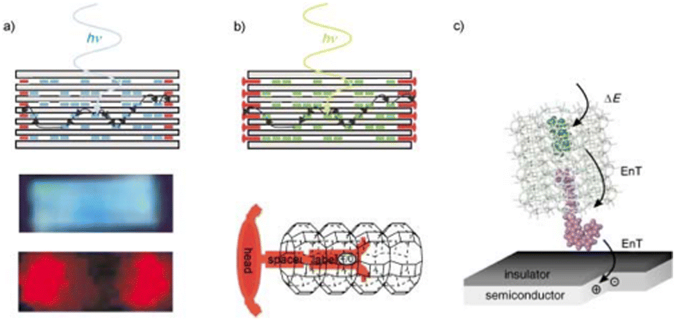 | ||
| Fig. 4 (a) Top: Dye-loaded zeolite L antenna; blue-emitting donors inside the zeolite L transfer electronic excitation energy to red-emitting acceptors at the ends of the cylindrical crystal. Middle and bottom: fluorescence microscope images of an approximately 2000-nm-long crystal containing DMPOPOP in the middle part (blue, polariser parallel) and Ox+ at both ends (red, polariser perpendicular) on selective DMPOPOP excitation. (b) Top: Antenna system with stopcock molecules as external traps and bottom: a schematic representation of a stopcock at the end of a zeolite L channel. The stopcock consists of a head, a spacer, and a label. (c) Energy transfer (EnT) from a photonic antenna to a semiconductor, creating an electron–hole pair in the semiconductor (radiationless near-field process). Reproduced from ref. 70 with permission from the Wiley-VCH GmbH. Copyright 2003. | ||
A significant aspect of the excitation of e–h pairs via energy transfer from molecules at separation less than ∼5nm at the surface of an indirect band gap semiconductor such as Si is the consideration of momentum conservation. When a photon's momentum is effectively zero, a transition in an indirect band gap semiconductor needs to be phonon assisted. Because the energy is provided non-radiatively by a molecular excited state arising from a localised state, the momentum is ill-defined, and momentum conservation can, in principle, be bypassed.74
One of our early work employed the Langmuir–Blodgett (LB) technique for controlled deposition of dye monolayers to study the effect of Si crystal orientation on the FRET efficency.75,76 The LB method can prepare uniform monolayers and allows a good control on the spacer thickness down to ∼2.5 nm. We used mixed monolayers of a prototypical luminescent cyanine dye molecule together with stearic acid and studied the luminescence quenching as a function of distance to the Si surface using inert stearic acid LB films as spacers (Fig. 5A). Our study on fluorescence intensity and decay measurements revealed strong quenching at short distances from the Si surface, but showed no dependence on the Si crystal orientation (100 or 111).75,76 Limited evidence exists about the role of Si crystal orientation in luminescence quenching or the FRET rate. Such a study can shed light on the role of crystal momentum in the FRET process and the necessity of phonon assistance for momentum conservation.
 | ||
Fig. 5 (A) Schematic cross section of the structure of a dye monolayer deposited on a glass substrate. (a) Four layers of cadmium stearate were initially deposited followed by (b) a monolayer of 3,3′-dioctadecyloxacarbocyanine (DiO) at a mixing ratio 1![[thin space (1/6-em)]](https://www.rsc.org/images/entities/char_2009.gif) :100 or 1:1000 with stearic acid. (B) Schematic illustration of the stepped LB film structure on silicon fabricated from (a) cadmium stearate monolayers with each step consisting of two layers of SA. Step 0 consists of the native oxide present on the silicon surface. (b) A uniform monolayer DiO:SA (1:100) was deposited on top to cover the whole stepped structure. Reproduced from ref. 75 with permission from Elsevier. Copyright 2008. (C) Plots of monomer and dimer lifetime ratios with respect to the lifetimes on glass as a function of distance to the silicon surface averaged over three separate experiments. The lifetimes have been estimated from a single exponential decay on the determined amplitudes for the monomer and dimer respectively determined from a decomposition of the TRES spectra in the time region 0–4.5 ns, step 0.5 ns for the monomer and 2.5–4.5 ns for the dimer; see text for details. The fitted line is a Förster 3rd power law line. Estimated Förster radius is 5.5 ± 0.5 nm. Error bars shown are 10%. Reproduced from ref. 77 with permission from Elsevier B. V. Copyright 2010. :100 or 1:1000 with stearic acid. (B) Schematic illustration of the stepped LB film structure on silicon fabricated from (a) cadmium stearate monolayers with each step consisting of two layers of SA. Step 0 consists of the native oxide present on the silicon surface. (b) A uniform monolayer DiO:SA (1:100) was deposited on top to cover the whole stepped structure. Reproduced from ref. 75 with permission from Elsevier. Copyright 2008. (C) Plots of monomer and dimer lifetime ratios with respect to the lifetimes on glass as a function of distance to the silicon surface averaged over three separate experiments. The lifetimes have been estimated from a single exponential decay on the determined amplitudes for the monomer and dimer respectively determined from a decomposition of the TRES spectra in the time region 0–4.5 ns, step 0.5 ns for the monomer and 2.5–4.5 ns for the dimer; see text for details. The fitted line is a Förster 3rd power law line. Estimated Förster radius is 5.5 ± 0.5 nm. Error bars shown are 10%. Reproduced from ref. 77 with permission from Elsevier B. V. Copyright 2010. | ||
In a further study using LB films,77 we observed significant quenching for distances less than 10 nm with an estimated Förster radius of 5.5 nm. As mentioned earlier intralayer energy transfer between the dyes on a monolayer can affect the observed luminescence quenching. We were able to separate the fluorescence quenching contribution from the monomers and dimers present in the LB monolayer and found the transfer rate from monomers to exceed the transfer rate from dimers by more than a factor of two (Fig. 5B). We showed that different ratios of a cyanine dye mixed with stearic acid can promote dimers and higher aggregates present in the monolayer that exhibit strong intralayer energy transfer competing with energy transfer to silicon.78
Bioinspired sensitisation of Si was demonstrated by Zajac et al.79 who reported non-radiative energy transfer from enhanced green fluorescent protein (EGFP) to a Si substrate, resulting in 98% photoluminescence quenching. The data were measured using fluorescence intensity, but the expected d−3 distance dependence was not observed, possibly due to the sensitivity of intensity measurements to variations in the emission radiation pattern.
In our subsequent work,54,55 we introduced a novel and more precise description of the mechanism occurring between dye molecules in proximity to silicon by introducing the photon tunnelling process. We investigated photon tunnelling experimentally using a multimode ultrathin Si waveguide and carried out a detailed distance dependent study of the luminescence properties of molecules on the Si waveguide surface. The geometry of the samples under study is shown in Fig. 6a.
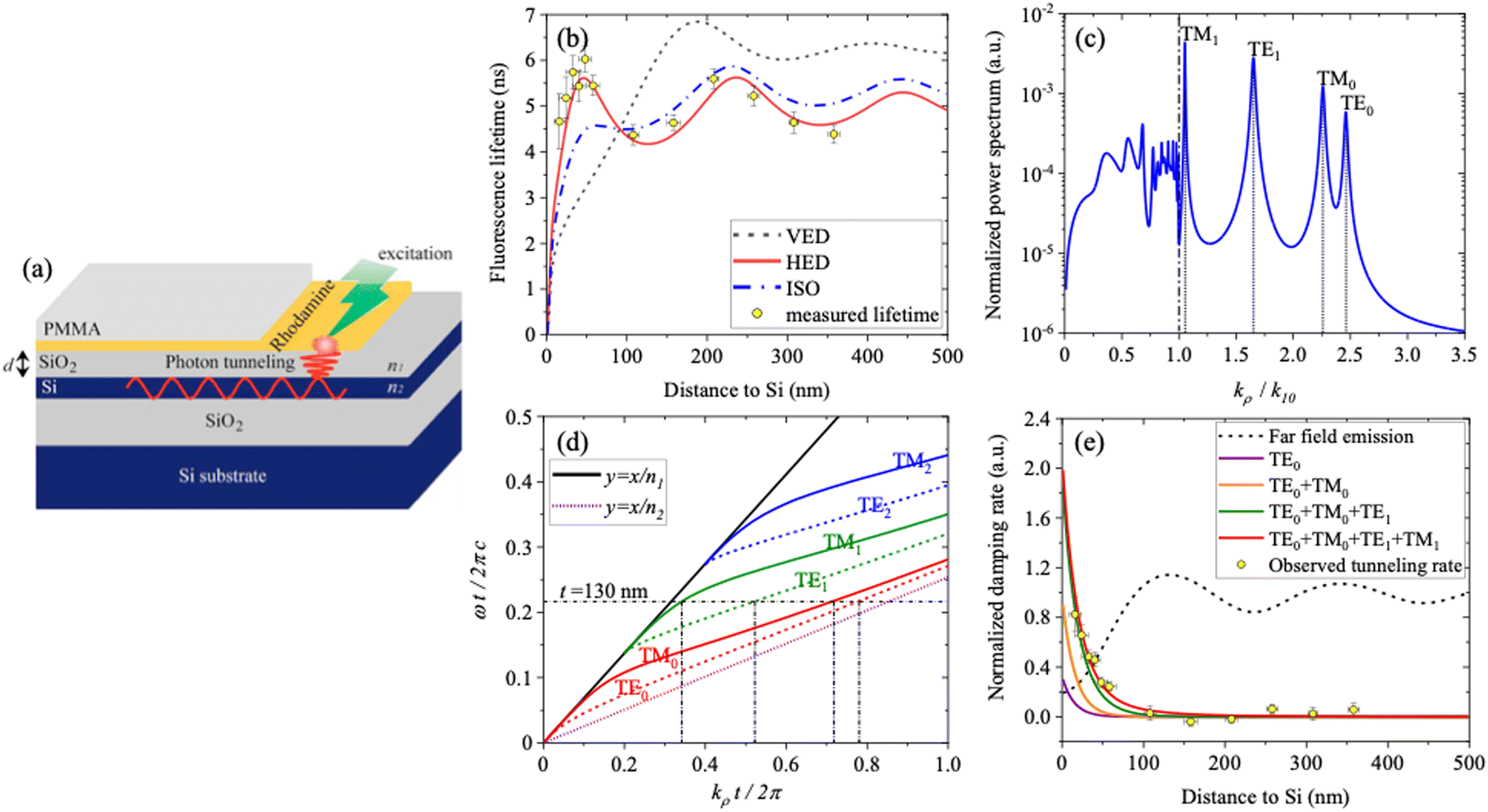 | ||
| Fig. 6 (a) Sample structure for investigating photon tunnelling from a submonolayer of fluorescent molecules to an ultrathin (d = 130 nm) crystalline silicon waveguide. (b) Comparison of fluorescence lifetime with a classical dipole model for different dipole orientations (c) power spectrum of a horizontal electric dipole emitting near the silicon waveguide (d) dispersion relation of the silicon waveguide and (e) comparison of modelled and observed photon tunnelling rates. Reproduced from ref. 55 with permission from Optica publishing group. Copyright 2020. | ||
All the samples (15 mm × 15 mm) were fabricated on a silicon-on-insulator (SOI) substrate. The thickness of the Si device layer and the silicon dioxide (SiO2) box layer was 130 ± 5 nm and 1934 ± 5 nm, respectively. The thickness of the spacer layer between the dye (rhodamine 6G) and the Si device layer was varied using SiO2 films deposited by plasma-enhanced chemical vapor deposition (PECVD). The dye sub-monolayer was obtained by spin-coating of a few drops of dilute alcohol solution of rhodamine 6G. To improve the stability of rhodamine, a final capping layer of polymethyl methacrylate (PMMA) with thickness around 70 nm was deposited on all the samples by spin-coating.
The measured fluorescence lifetime as a function of the emitter–Si distance is modelled well by the CPS theory, shown in Fig. 6b. The power spectrum of the dipole emitter is plotted in Fig. 6c, where the distinct peaks are related to the waveguide modes supported by the Si waveguide after solving the dispersion relation of the Si waveguide (Fig. 6d).
The energy transfer efficiency, which is crucial for comparing different power dissipation channels, was estimated at 80% based on the ratio of photon tunnelling to fluorescence emission rates. Accounting for reverse tunnelling, where molecules couple power out via evanescent waves, is also an important parameter that will need to be addressed in future studies. These experiments and the accompanying theoretical analysis are key to the design of hybrid optoelectronic devices that exploit evanescent photon coupling into waveguide modes.
Quantum dot monolayers on the surface of Si
Several studies on Si sensitisation have investigated quantum dots as energy donors. Nguyen et al.80,81 studied CdSe/ZnS nanocrystals emitting at 560 nm and demonstrated non-radiative energy transfer to Si consistent with the CPS model (∼ d−3). They reported a donor quantum yield of approximately 85% dominated by FRET for donors located 4 nm from the Si surface (Fig. 7). | ||
| Fig. 7 Different NQD/Si nanomembrane structures used to extract the relative participation of various decay channels: schematically displayed are NRET and RET processes from NQDs into the underlying Si slab as well as into SiO2 substrate (on the rightmost structure). NRET role is strongly diminished with a thicker spacer (the leftmost structure), while the waveguiding modes in Si are excited quite efficiently. (top left) SEM cross-sectional image of one of the experimental structures showing the uniformity of the Si membrane thickness. (top right) AFM images of NQDs attached via carboxy-terminated alkyl chains on an oxide-free Si nanomembrane surface. The 5 × 5 μm image emphasises the homogeneity of the NQDs’ monolayer attachment, while the 1 × 1 μm confirms the individuality of the NQDs to minimise interdot ET effects. (a) PL dynamics for NQDs grafted on bare Si nanomembranes with thicknesses t = 25, 50, 70, 90, 110, 150, and 290 nm compared to NQDs on the reference glass substrate (top curve). Slowest dynamics measure decay time τ = 4.5 ns and correspond to the NQDs on ultrathin (t = 25 and 50 nm) Si slabs. (b) and (c) Dynamics for NQDs grafted on t = 22, 150, and 290 nm Si slabs that have spacer layers of thermal SiO2 of thicknesses d = 4.5 nm. Reproduced from ref. 81 with permission from American Chemical Society. Copyright 2012. | ||
A similar d−3 distance dependence was observed by Andreakou et al.82 for non-radiative energy transfer from PbS quantum dots emitting at 890 nm, with an energy transfer efficiency of 46% observed at a donor–Si separation of 5 nm. Nimmo et al.83 investigated CdSe/ZnS quantum dots of various sizes, emitting in the 545–800 nm range, and found that non-radiative energy transfer exhibited a maximum quantum yield exceeding 70% for the smallest dots (4–4.6 nm) emitting near 550 nm.
Relatively thick SiO2 and Al2O3 spacing layers were employed by Yeltik et al.84,85 to study phonon-assisted energy transfer from CdSe/ZnS quantum dots emitting at 580 nm, observing a maximum transfer efficiency exceeding 50% at 370 K, with a notable dependence on temperature. Noteworthily, modelling has shown that quantum dot size variability can influence both the mechanism and efficiency of energy transfer to silicon.86 A d−1 distance dependence of energy transfer from quantum well nanoplatelets was observed at a donor–Si separation of 20 nm.87
A study conducted by Rupich et al.88 describes a novel method for preparing quantum dot multilayers (PL emission at 600 nm), demonstrating both radiative and non-radiative energy transfer to silicon with 60% efficiency. This work was followed by a study using giant CdSe/CdS quantum dots (radius 9–10 nm, emission around 650 nm), focusing on radiative and non-radiative energy transfer from both excitons and biexcitons.89
Graphene quantum dots (GQDs) are extensively utilised in various solar cell technologies due to their exceptional optical and electrical properties.90,91 For instance, they function as light-harvesting sensitisers in dye(dot)-sensitised solar cells via charge transfer mechanisms,92 and as light-harvesting sites in organic solar cells through FRET.93 GQDs also serve as luminescent downshifting layers94 in copper indium gallium selenide (CIGS)95 and Si solar cells,96 and as electron/hole transport layers in perovskite97 and heterojunction Si solar cells.98 Despite the significant potential of GQDs for Si sensitisation, detailed investigations into the energy transfer mechanisms from GQDs to Si have yet to be reported.
Studies on QD sensitisation of Si have shown that FRET typically follows a d−3 distance dependence, with transfer efficiencies ranging from about 46% to over 70%, depending on quantum dot size, emission wavelength, temperature and separation distance. Energy transfer through both nonradiative and radiative pathways has been recognised as an efficient mechanism to couple excitonic energy to Si. Optically dense QD layers that can harvest most of the incident solar light while maintaining high luminescence quantum yields must be developed, similar to fluorescent molecules. It is important to note that luminescence quenching observed with dyes or QDs on the surface of Si does not constitute unequivocal proof of electron–hole pair generation via FRET. Further experiments, such as photoconductivity or silicon fluorescence enhancement measurements, are required to confirm e–h pair generation through this mechanism.
Engineering the dye–Si interface
The Si surface plays a dominant role in optoelectronics.99,100 In particular, the chemical modification of Si(111) surfaces has seen an active area of research for the past three decades.101–108 The important aspect in the Si surface chemistry of interest in this work is the production of oxide free Si surfaces which result in stable monolayers of molecules with a direct covalent bond (Si–C) on the Si surface. The first step is the removal of the native oxide (∼2 nm) in Si via etching using wet chemistry producing hydrogen-terminated Si(111) surfaces.109 The Si(111)–H surface can then be used for further functionalisation with a host of different reagents.We are interested in producing stable monolayers on the Si surface that can serve a dual functionality. The first aspect creates a monolayer that can passivate the Si surface.110,111 The role of passivation is important as it eliminates surface traps or dangling bonds and reduce surface e–h recombination that can be a source of unwanted current losses. This is even more important towards using Si thickness (∼1 μm) which is less than two orders of magnitude of what is currently used in Si (∼150 μm) solar cells today.
The second desired function is the ability to further functionalise the monolayer with suitable chromophore molecules that can inject excited state energy into Si resulting in the production of e–h pairs. A very important aspect is the non-radiative interaction between the excited state molecule and the Si surface. This can only efficiently be achieved for distances less than ∼5 nm. Therefore, the dual function of passivation and further functionalisation with chromophores on Si can be achieved using organic monolayers of only a few molecules thick. This molecular approach to Si surface modification forms a very useful platform to test near field excitation of Si and develop new solar cell paradigms.
Chemical passivation of Si surfaces
Chemical passivation of Si surfaces using covalent attachment of organic monolayers has been investigated in the literature resulting in stable, oxide free surfaces with comparable e–h recombination lifetimes with those from thick (∼120 nm) thermal oxide produced Si surfaces. The e–h recombination lifetime can be monitored using a host of different experimental methods.112The measured effective lifetime contains contributions from both the bulk and surface e–h recombination.112 A usual method applied to separate the surface contribution from the bulk is to measure the e–h recombination while having passivated the surface, for example using quinhydrone–methanol,113 or silicon nitride films.114 In most cases, a high-quality Si substrate is used where bulk recombination lifetimes can be assumed to be greater than 1 ms and therefore neglected leaving the major contribution to be surface e–h recombination.
We have chosen a simple chlorination/alkylation reaction115 using Grignard reagents that produce oxide free Si(111) surfaces displaying excellent passivation and being resistant to further oxidation (Scheme 1). We observed large surface photovoltages (SPV) associated with significantly improved minority carrier lifetimes.116 The observed photovoltage results from large band bending and assigned to an increase in the accumulation of charges on the Si surface during the methylation reaction. An interesting aspect of this observation is that the trapped charges prevent e–h recombination at the Si surface via a field effect.
 | ||
| Scheme 1 Route for the attachment of alkyl monolayers on silicon. Reproduced from ref. 117. The Royal Society of Chemistry. Copyright 2013. | ||
We further investigated the influence of using different chain length alkyl layers on the Si(111) surface. The monolayers produced showed good stability under ambient conditions and maintained effective passivation for over 1000 hours. We found a linear logarithmic relationship between the recombination lifetime and the observed surface photovoltage,117 confirming the observation that surface band bending reduces e–h recombination at the surface.
In a further work, a methodology was developed using a kelvin probe to estimate the surface recombination current from SPV measurements.118 Good agreement was found between the recombination lifetime values measured with the kelvin probe and the more traditional Sinton lifetime tester. The kelvin probe method has the advantage of obtaining a 2D map of the surface recombination velocity for each sample producing surface sensitive 2D maps.
A novel study119 investigated the effect of distance from charged molecules on the Si(111) surface using dicarboxylic acids with variable carbon chain lengths. A negative charge was generated on the free carboxylic acid end by immersion in base compensated by a positive space-charge region near the Si surface. Preliminary results showed a linear correlation between the chain length and the measured SPV and recombination lifetime.
As seen the use of organic monolayers for the passivation of silicon produces well passivated Si(111) surfaces that display long charge carrier lifetimes and low surface recombination velocities. Oxide free surfaces that result from covalent attachment of alkyl layers can eliminate surface traps and broken bonds. We have shown that during the alkylation procedure charges trapped on the surface aid in the overall passivation from a field effect. Further work is required to identify the nature and role of the trapped charges on the Si interface. Overall, the passivation step using organic monolayers plays an important role towards realisation of the photosensitised Si solar cell concept.
Chromophore attachment of Si surfaces
The removal of the native oxide (∼2nm) from the Si surface and the subsequent chemical modification of the surface offers the advantage of accessing sub-nanometre distances to the surface of Si. For example, a methyl terminated Si(111) surface is only 2–3 Å thick.120 By varying the number of atoms on the covalently attached molecule the separation to the Si surface can be altered within the crucial 1 nm separation range, not studied before in detail.We have attached a modified protoporphyrin IX (PpIX) analogue on the surface of Si(111) and varied the distance to the surface using a diol linker with different numbers of carbon atoms. A chlorine terminated Si(111) surface was used to attach the appropriate diol linker group followed by the attachment of the PpIX moiety (Fig. 8a).121
 | ||
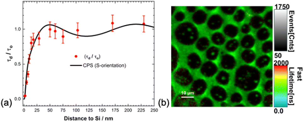
| Fig. 8 (a) Attachment of the protoporphyrin IX acyl chloride (PpIX-Cl) to the Si(111) surface. (b) A molecular model of the silicon(111) surface with diols and a PpIX molecule covalently attached. (c) The fluorescence lifetime for various diol linked porphyrin surfaces. (d) Experimental points are fitted by Chance–Prock–Sibley theory (CPS, full blue line). Also shown, by dashed and dotted lines, are separate contributions from different mechanisms. Reproduced from ref. 121. The Royal Society of Chemistry. Copyright 2017. | ||
We used different carbon diol chain lengths from two to ten to vary the distance of the PpIX molecule to the Si surface. A molecular model of a PpIX molecule linked to an ethane diol on the Si(111) is shown in Fig. 8b. The large pi-ring is expected to minimise its energy by adopting a parallel orientation with the SI surface. We measured the fluorescence decays at the maximum emission wavelength (670 nm) of PpIX as a function of distance to the Si surface (Fig. 8c). We observe a significant shortening of the decay as the separation of PpIX is reduced from 15 Å to 5 Å. The measured decay lifetimes are fitted to CPS theory showing a d−3 distance dependence with an estimated Förster radius of R0 = 2.7 nm (Fig. 8d). This study allowed us to measure distances less than 2 nm between the chromophore-silicon demonstrating a Förster-like energy transfer.
There are, of course, experimental limitations in measuring the chromophore–Si separation, in this case constrained by the model fit used in variable angle spectroscopic ellipsometry (VASE), while a topographical measurement would be more suitable for such small distances.122 Moreover, the orientation of the diol layers on the Si surface has not been fully characterised, and their passivation effect remains untested. The chromophore–Si separation regime below 2 nm is critical for identifying the energy transfer mechanism whether Förster-type or Dexter. Furthermore, the role of chromophore dipole orientation, as predicted by the CPS (see the Theoretical foundations section), remains largely unexplored experimentally.
In a subsequent study we synthesised vinyl Si(111), (Si-vinyl), and allyl Si(111) (Si-Allyl) surfaces, which were subsequently functionalised via a Heck coupling reaction with a perylene derivative.123 XPS measurements in the Si 2p region showed the preparation of an oxide free surface and the C1s region confirmed the vinyl attachment with an estimated 95% molecular coverage. We investigated the passivation properties of the Si-vinyl and Si-allyl surfaces by measuring the Si emission spectra and time-resolved decays (∼1120 nm). The emission spectra showed significant improvement compared to native oxide or chlorinated silicon. In addition, the estimated Si emission lifetimes indicated up to two orders of magnitude enhancement in recombination lifetimes relative to native oxide Si samples, confirming effective passivation.
We used a combination of perylene molecule attachment to the Si–vinyl and Si–allyl surfaces and LB monolayer deposition of a perylene derivative on methylated Si(111) substrates to investigate the fluorescence quenching in the region of less than 5 nm to the Si surface. The chromophore attachment was confirmed by XPS measurements with an estimated ∼5% coverage. Furthermore, FLIM measurements showed the presence of the perylene molecules on the Si(111) surface (Fig. 9). Our fluorescence decay measurements showed quenching up to 90% of the lifetimes and an estimated Förster radius of 2.5 nm (Fig. 9).
 | ||
| Fig. 9 Fluorescence lifetime imaging (FLIM) scans of (a) Si–Vinyl–Pe surface, (b) Si–Allyl–Pe surface. (c) Normalised fluorescence decay curves for different perylene surfaces. (d) The experimental fluorescence lifetimes of different perylene functionalised surfaces fitted to Chance–Prock–Silbey (CPS, full blue line) and to an inverse cubic (Förster) fit. Reproduced from ref. 123. The Royal Society of Chemistry. Copyright 2020. | ||
It is worth noting that the Heck coupling reaction uses trace amounts of Pd catalyst which are present in the XPS spectra even after multiple washes. The presence of Pd induces a significant decrease in the recombination lifetime of silicon, indicating metal contamination.124 Therefore, future functionalisation of Si surfaces will have to follow a metal catalyst free route in order to preserve the passivation properties of the organic monolayer and prevent metal contamination.125 Silicon surface chemistry offers a promising route to passivate and further functionalise the Si surface, enabling access to the critical dye-Si separation below 2 nm, which is essential for advancing our understanding of silicon photosensitisation.
Triplet sensitisation of silicon
Dexter in his original proposal for the sensitisation of the photovoltaic effect suggested the use of triplet excitons generated by inter-system crossing or by exciton fission. He argued for the longer diffusion lengths that triplet excitons exhibit, enabling them to reach the surface. Exciton fission converts a singlet exciton to two triplet excitons and holds the promise to improve the efficiency of Si solar cells beyond the single junction efficiency limit.126 Most studies of exciton quenching by silicon to date have focused on singlet excited states. In recent years, singlet fission has gained significant attention for its potential application in silicon photovoltaics.127,128We recently reported up to 95% triplet exciton quenching from a Si surface.129 The triplet excitons were generated via intersystem crossing from a rhenium fac-tricarbonyl bipyridine complex appended with a sixteen-carbon chain (ReC16) deposited as an LB monolayer on Si substrates at different ReC16–Si separations. We conducted phosphorescence lifetime imaging microscopy (PLIM) measurements for ReC16–Si separations from 2 to 250 nm (Fig. 10). The phosphorescence lifetimes show good agreement with a modified CPS model. At distances less than 10 nm we observe significant quenching (up to 95%) of the phosphorescence indicative of efficient triplet FRET to silicon. This study showcases the first observation of a distance dependent triplet exciton quenching from an organometallic complex on silicon and demonstrates the potential of triplet exciton energy transfer for silicon photosensitisation.
 | ||
| Fig. 10 (a) Normalised phosphorescence (triplet) lifetime versus distance for the ReC16 monolayer deposited on c-Si. Experimental points are fitted to a modified Chance–Prock–Silbey (CPS, full line) theory with a parallel dipole (S) orientation with quantum yield, QY = 75%. (b) Phosphorescence Lifetime Image Microscopy (PLIM) on a Rhenium monolayer. Reproduced from ref. 129. The Royal Society of Chemistry. Copyright 2024. | ||
Progress towards a photosensitised Si solar cell
The photosensitisation of Si offers a new paradigm in photovoltaic design by separating the functions of light absorption and charge separation. This concept draws directly from natural photosynthesis, where the light-harvesting antenna absorbs incident light and transfers the excitation energy to a reaction centre. In a similar fashion, energy harvested by molecular systems near the Si surface can be transferred either via a Förster-like near-field dipole–dipole interaction, effective at separations below 5 nm, or via photon tunnelling mediated by the evanescent field at larger separations (10–200 nm). These mechanisms allow optical excitation in Si without the direct absorption of photons and, critically, without the momentum constraints typically imposed by indirect bandgap transitions. Surface functionalisation through organic monolayers and covalent attachment of dyes offers control over molecule–Si separation within a few nanometres, enabling the simultaneous passivation of the Si surface and efficient energy transfer.Despite these advances, key challenges remain. Although luminescence quenching studies suggest energy transfer from dyes and quantum dots to Si, direct evidence of electron–hole pair generation is still limited. Measurements such as photoconductivity or silicon photoluminescence enhancement are needed to confirm e–h pair generation via near-field mechanisms. In addition, the orientation and aggregation of dyes on the surface, as well as contamination from metal catalysts used in coupling reactions, can adversely affect energy transfer efficiency and charge carrier lifetimes. A key challenge is the unambiguous demonstration that momentum conservation is bypassed during non-radiative energy transfer to Si and that dipole orientation at the interface critically influences the efficiency of energy transfer. Addressing these challenges is essential for the development of a viable photosensitised Si device.
This paper has covered so far, several key aspects towards the realisation of a photosensitised Si solar cell. These include: the importance of electrostatic near-field interaction (distance <5 nm) between the excited chromophore (dye or QD) and the Si surface to enable efficient excitation of e–h pairs; the necessity of chemical passivation using a monolayer on the Si surface to prevent rapid surface recombination of generated charge carriers; and the potential for further functionalisation of the organic monolayer with suitable chromophores (e.g., porphyrin and perylene molecules) to serve as terminal traps for harvested energy.
Compared with today's dye-sensitised solar cells,130 the proposed photosensitised Si solar cell eliminates the electrolyte and counter electrode. Therefore, not only will the production be simplified considerably, but also the efficiency should rise by removing the highest series resistance in the cell – the electrolyte – leading to a considerably higher fill factor. It will also improve the long-term stability. Not only is the difficult sealing of the electrolyte avoided, but also the lifetime of the most sensitive part of the cell, the dye, should increase, since it will no longer act as a redox couple.
We have touched on, but not explored in detail, the development of suitable light-harvesting structures (LHS) with high absorption efficiency and long exciton diffusion lengths, such as dye-loaded zeolite L systems. Developing new luminophores, whether quantum dots or dyes, that emit efficiently in the near-infrared (NIR) should be a priority to match the band gap of c-Si (λ ∼ 1110 nm). This will enable us to better understand the roles of phonon assistance and the dielectric constant in indirect band gap transitions. This discussion has not addressed near-field interactions involving plasmonic structures or alternative types of solar cells131 and has focused exclusively on Si-based devices. These topics are some examples that outline future directions toward the realisation of a sensitised Si device.
In terms of modelling, the classical CPS theory provides a useful framework for describing molecular fluorescence near surfaces such as Si, but it lacks specificity regarding the dominant energy transfer mechanisms at different molecule–Si separations. We have identified FRET and photon tunnelling as the key processes governing fluorescence quenching near c-Si. Fig. 11 shows the experimentally resolved contributions, including far-field emission, photon tunnelling, and FRET, and illustrates their respective roles. At separations below 10 nm, FRET dominates the energy transfer process. In the intermediate range, approximately 10 to 200 nm, photon tunnelling becomes the primary decay channel. For distances exceeding 200 nm, interference between the emitted and reflected electromagnetic fields leads to periodic oscillations in the fluorescence decay rate.123 The overall measured decay rate is well described by the sum of these distinct contributions (FRET, photon tunnelling, and far field interference). The predominance of FRET at short distances (<5 nm) is further supported by experiments using porphyrin molecules directly bound to the Si surface, where the contribution from photon tunnelling is found to be insignificant.121
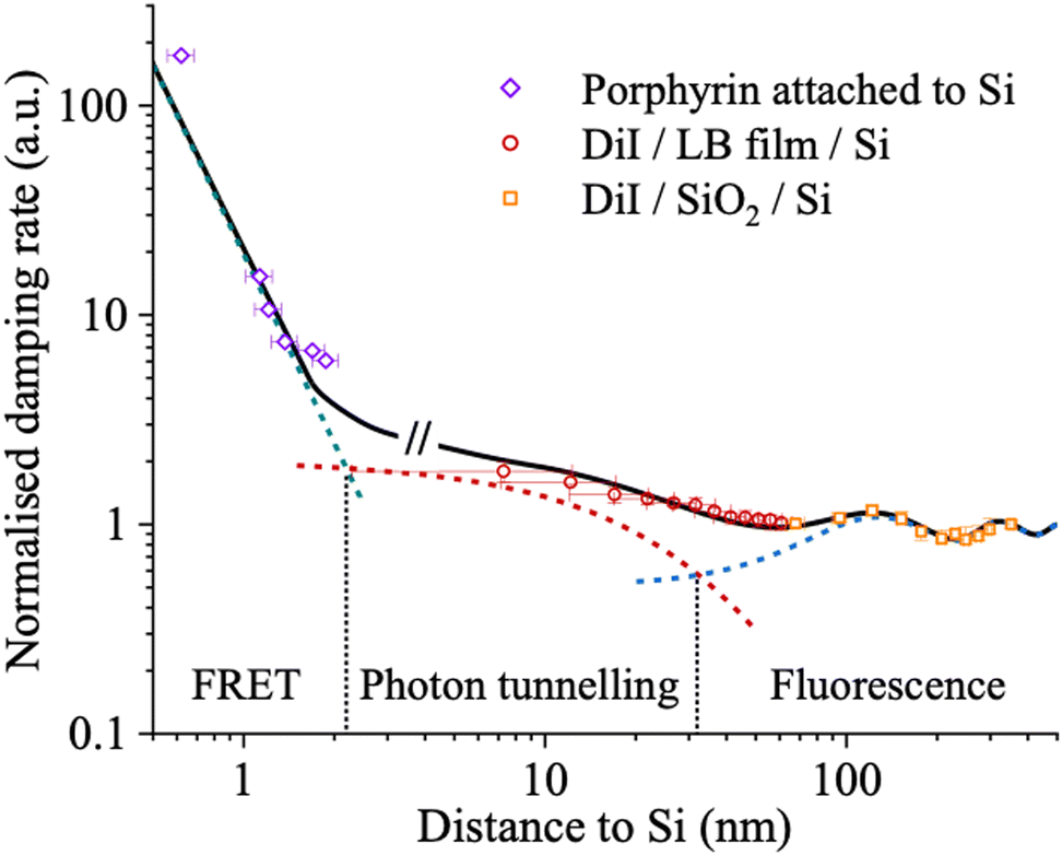 | ||
| Fig. 11 The theoretical distance-dependent dipole damping rate (solid curve) is compared with the measured rates, determined from the inverse fluorescence lifetimes (symbols), revealing distinct energy transfer channels (dashed line). For a porphyrin dye covalently attached to the surface of silicon, the dominant energy transfer channel is FRET at such close distance range (several nanometres). For intermediate distance range (several hundreds of nanometres) photon tunnelling becomes the prevailing process. At greater distances, the molecular dipole primarily dissipates power through molecular fluorescence. A theoretical model combining photon tunnelling and fluorescence accurately describes the distance-dependent fluorescence lifetime of a carbocyanine dye, 1,1′-dioctadecyl-3,3,3′,3′-Tetramethylindocarbocyanine perchlorate (DiI), near a silicon surface, utilising either Langmuir–Blodgett (LB) films or silicon dioxide (SiO2) films as spacer layers. Data reproduced from ref. 121 and 123. The Royal Society of Chemistry. Copyright 2017 and 2020. | ||
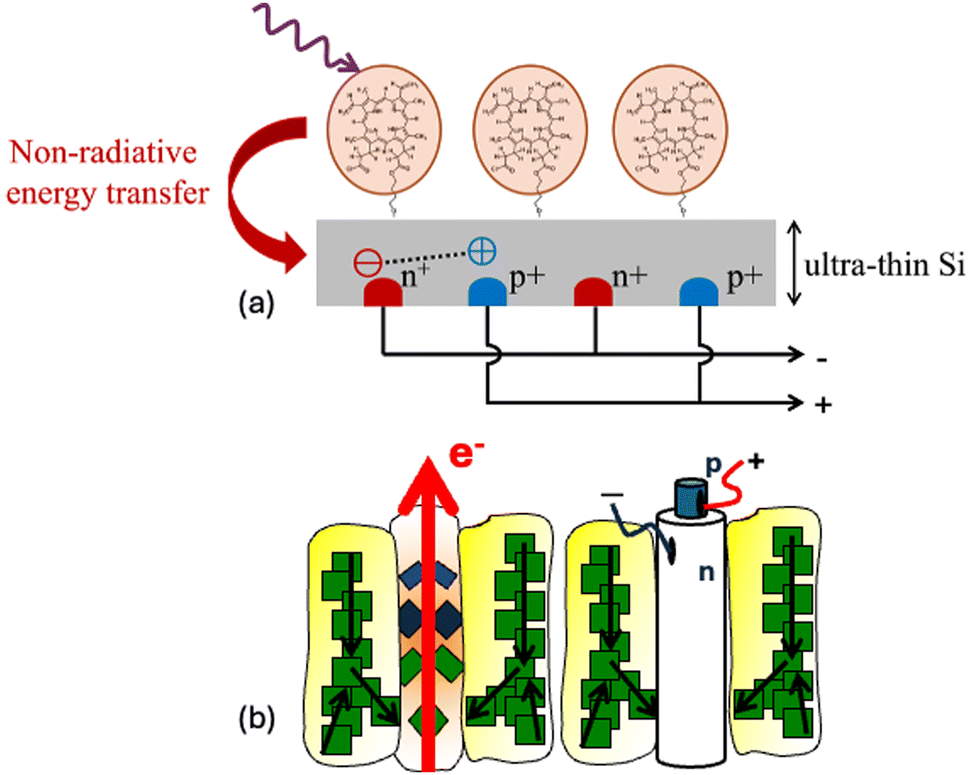
In terms of progress, the first realisation of a photosensitised Si solar cell was presented by MacQueen et al.132 incorporating tetracene into a heterojunction crystalline device, although direct evidence of energy transfer from tetracene to silicon was not confirmed. A Si photosensitisation device was demonstrated by Baldo's group133 where energy transfer from tetracene led to the creation of e–h pairs in silicon, evidenced by enhanced silicon photoluminescence. (Fig. 12). The exact mechanism of energy transfer has not been definitively identified, due to competing channels of singlet and triplet energy transfer to Si. A following study by the same group134 demonstrated that the presence of a hafnium oxynitride layer is crucial for triplet exciton sensitisation, since the nitrogen vacancy defects introduce states near the Si band edge. The same group has recently demonstrated a microwire singlet fission Si solar cell.135
 | ||
| Fig. 12 (a) Flow diagram summarizing the two pathways that increase silicon photoluminescence. Following photoexcitation of tetracene (blue) or silicon (dark purple), electric-field-effect passivation (orange charges) is caused by exciton dissociation at the interface or charge diffusion from the silicon. Additional electron–hole pairs in silicon can also be created by singlet exciton fission in tetracene (green) and triplet energy transfer (light red). (b) Excitation spectrum showing the beneficial influence of the tetracene coating on a photoluminescent silicon sample. The contributions of the silicon absorption (red dashed line) and the tetracene absorption (green dashed line) are shown. Vertical error bars are 1σ; horizontal error bars are the spectral width of the excitation source at an intensity of e−2; n = 1600. Inset, schematic of the measurement method. Reproduced from ref. 133 with permission from Springer Nature. Copyright 2019. | ||
More recently Humayun et al.87 investigated energy transfer from quasi-2D colloidal quantum well nanoplatelets leveraging higher absorption and observing enhanced photocurrent response from an ultra-thin Si photodetector. Photoconductivity enhancement has also been reported for rhodamine 6G molecules adsorbed on Si substrates or powders.136
A novel study was conducted by Goryaev137 on photoconductivity measurements of Rhodamine 6G molecules adsorbed on Si powder samples composed of micron-sized crystals, which were pressed onto a quartz plate to form a pellet. The results show an increase in photoconductivity, by more than an order of magnitude compared to non-dyed samples, in the spectral region where the dyes absorb. The observed increase in photoconductivity is not attributed to the dye itself, since both powder and thin film dye layers show low dark conductivity and no photoconductivity. At higher dye concentrations the photoconductivity decreases due to a solid film forming on the powered crystals hindering charge transport. Although the authors provide limited experimental details, the results are nonetheless impressive and merit further investigation.
Our discussion so far highlights the challenges in assembling a fully functional Si sensitised solar cell with improved efficiency. As such, standard device-level metrics are not yet available, since no complete and operational photosensitised Si solar cell has been realised to date. Energy transfer efficiencies ranging from 50% to 95%, depending on the emission wavelength, have been observed for both quantum dots and molecular dyes on Si, based on luminescence quenching measurements at sub-5 nm distances. Photocurrent enhancement by a factor of three has also been reported, although such studies remain limited in number.
Future directions toward the realisation of such a device could focus on planar structures similar to the current technology but replacing Si wafers with a thin crystalline layer (Fig. 13) or employing microwire architectures.138 Alternatively, an approach similar to that used in dye-sensitised solar cells using powdered Si coated with a dye monolayer, as presented earlier, and assembling it into a functional device, can be followed. There is significant potential for Si sensitisation on the nanoscale, which could affect the entire optoelectronic industry.
 | ||
| Fig. 13 (a) Schematic of an example of a photosensitised ultrathin c-Si solar cell with interdigitated back contacts. (b) Conceptual analogy between natural photosynthesis and silicon photosensitisation. In both systems, light is absorbed by light harvesting structures and the excitation energy is transferred to a central site (reaction centre or Si microwire) where charge separation and electron generation occur. | ||
Conclusions and outlook
We have shown historical and recent advances in the realisation of a photosensitised Si solar cell. We presented theoretical and experimental studies to highlight the importance of the near filed interaction between the luminophore and the Si surface at a distance below 5 nm.We showed that the photosensitisation of silicon by proximal fluorescent molecules can proceed via two distinct pathways. One mechanism resembles FRET, a dipole–dipole interaction well-established between fluorescent molecules. This FRET-like energy transfer typically dominates at very short separations, operating effectively when the distance between the fluorescent molecule and the Si surface is less than a few nanometres, consistent with the characteristic length scale of FRET. In contrast, the second mechanism, referred to as photon tunnelling, involves coupling via the evanescent field of the excited molecule into a manifold of optical states within the silicon.
Critically, this includes states that are normally inaccessible to direct illumination under Snell's Law, allowing the injected energy to propagate along the solar cell structure rather than being solely a localised, short-range transfer. The working distance for photon tunnelling can extend up to approximately 200 nanometres. This extended range facilitates efficient energy transfer from fluorescent molecules located relatively far from the Si surface, an advantage when thick molecular layers are deposited on the Si substrate to achieve efficient absorption of incident solar radiation. Furthermore, this molecule–Si scheme is important to the design and optimization of hybrid optoelectronic devices based on a photon management technique that allows the evanescent coupling of photons into individual waveguide modes.
Molecular and quantum dot (QD) systems have demonstrated promising energy transfer efficiencies, with FRET typically following a d−3 dependence being not evidence for e–h generation in Si. Further experimental techniques, such as photoconductivity or silicon fluorescence enhancement measurements, are required to establish clear proof of carrier injection via FRET. Accessing the critical few nanometre regime requires the development of oxide-free Si surfaces via surface chemistry that enables efficient passivation. The covalent attachment of dyes provides a valuable platform for assessing energy transfer processes.
To guide future progress, several key challenges and research directions must be addressed. The unambiguous confirmation of electron–hole pair generation via energy transfer remains essential. This will require systematic studies combining photoconductivity, photoluminescence, and device-level performance measurements. Controlling molecular orientation and preventing chromophore aggregation at the Si interface must be developed, particularly for dense or multilayered systems.
Further theoretical work is also needed to refine our understanding of phonon involvement in energy transfer to an indirect semiconductor at the nanoscale. Integration with emerging photophysical concepts such as singlet fission and triplet sensitisation offers exciting possibilities for exceeding single-junction limits.
In terms of device design, potential future architectures may include ultrathin crystalline Si films sensitised by broadband light-harvesting layers, or porous hybrid structures combining organic molecular collectors with interdigitated Si contacts. Applications may not be limited to photovoltaics, but extend to light sensors, photodetectors, or CMOS-compatible optoelectronic platforms. The photosensitised silicon concept is not only a promising route to more sustainable solar cell fabrication, but also a valuable experimental testbed for probing fundamental light–matter interactions in complex hybrid materials.
Si solar cells emerged as an offshoot of microelectronics in the early 1950s and have since developed into a major global industry. As integrated circuits continue to shrink in scale, the integration of molecular components may offer mutual benefits to both the photovoltaic and microelectronic sectors. The realisation of a photosensitised Si solar cell could open new avenues for next-generation solar energy technologies and hybrid electronic devices.
Conflicts of interest
There are no conflicts to declare.Data availability
No primary research results, software or code have been included, and no new data were generated or analysed as part of this review.Acknowledgements
LD acknowledges the financial support provided by the Leverhulme Trust (DS – 2017-036). LF acknowledges financial support from the National Natural Science Foundation of China (No. 61604138). BZ and TM would like to acknowledge support from project No. CZ.02.01.01/00/22_008/0004617–‘Energy Conversion and Storage’ by Programme Johannes Amos Comenius.Notes and references
- PV cell technology trends, https://www.pv-magazine.com/2023/08/29/pv-cell-technology-trends/, (accessed April 20, 2025).
- Global installed PV capacity tops 2 TW, https://www.pv-magazine.com/2024/11/13/global-installed-pv-capacity-tops-2-tw/, (accessed April 20, 2025).
- D. Meissner, K. Ernits, S. Gahr, L. Kapitan, M. Vetter, C. Glatz and R. Syed, Sol. Energy Mater. Sol. Cells, 2023, 252, 112160 CrossRef CAS.
- B. Hallam, M. Kim, R. Underwood, S. Drury, L. Wang and P. Dias, Sol. RRL, 2022, 6, 2200458 CrossRef.
- R. Deng, N. L. Chang, Z. Ouyang and C. M. Chong, Renewable Sustainable Energy Rev., 2019, 109, 532–550 CrossRef CAS.
- G. Wei, Y. Zhou, Z. Hou, Y. Li, Q. Liu, J. Chen and D. He, EES Sol., 2025, 1, 9–29 RSC.
- D. L. Dexter, J. Lumin., 1979, 18–19, 779–784 CrossRef CAS.
- S. Niwa, L.-J. Yu, K. Takeda, Y. Hirano, T. Kawakami, Z.-Y. Wang-Otomo and K. Miki, Nature, 2014, 508, 228–232 CrossRef CAS PubMed.
- H. M. Berman, Nucleic Acids Res., 2000, 28, 235–242 CrossRef CAS PubMed.
- R. P. D. Bank, RCSB PDB, https://www.rcsb.org/, (accessed April 26, 2025).
- R. Casillas, I. Papadopoulos, T. Ullrich, D. Thiel, A. Kunzmann and D. M. Guldi, Energy Environ. Sci., 2020, 13, 2741–2804 RSC.
- J. Lee, P. Jadhav, P. D. Reusswig, S. R. Yost, N. J. Thompson, D. N. Congreve, E. Hontz, T. Van Voorhis and M. A. Baldo, Acc. Chem. Res., 2013, 46, 1300–1311 CrossRef CAS PubMed.
- A. J. Baldacchino, M. I. Collins, M. P. Nielsen, T. W. Schmidt, D. R. McCamey and M. J. Y. Tayebjee, Chem. Phys. Rev., 2022, 3, 021304 CrossRef CAS.
- T. F. Schulze and T. W. Schmidt, Energy Environ. Sci., 2015, 8, 103–125 RSC.
- A. J. Carrod, V. Gray and K. Börjesson, Energy Environ. Sci., 2022, 15, 4982–5016 RSC.
- W. H. F. Talbot, Abstr. Pap. Printed Philos. Trans. R. Soc., London, 1843, 4, 120–121 Search PubMed.
- L. J. M. Daguerre, An historical and descriptive account of the various processes of the daguerréotype and the diorama, Mc. Lean, London, 1839 Search PubMed.
- E. Becquerel, C. R. Acad. Sci., 1839, 9, 145–149 Search PubMed.
- E. Becquerel, C. R. Acad. Sci., 1839, 9, 561–567 Search PubMed.
- The theory of the photographic process, ed. Thomas H. James, Macmillan, New York, 4th edn, 1977 Search PubMed.
- M. H. Rigollot, C. R. Acad. Sci., 1893, 116, 873–875 Search PubMed.
- H. Rigollot, J. Phys. Theor. Appl., 1897, 6, 520–525 CrossRef.
- R. Emerson and W. Arnold, J. Gen. Physiol., 1932, 16, 191–205 CrossRef CAS PubMed.
- H. Gaffron and K. Wohl, Naturwissenschaften, 1936, 24, 81–90 CrossRef CAS.
- T. L. Hill, Free energy transduction in biology: the steady-state kinetic and thermodynamic formalism, Academic Press, New York, 1977 Search PubMed.
- S. E. Sheppard, R. H. Lambert and R. D. Walker, J. Chem. Phys., 1939, 7, 265–273 CrossRef CAS.
- S. E. Sheppard, R. H. Lambert and R. D. Walker, J. Chem. Phys., 1939, 7, 426–436 CrossRef CAS.
- S. E. Sheppard, R. H. Lambert and R. D. Walker, J. Chem. Phys., 1941, 9, 96–113 CrossRef CAS.
- J. A. Leermakers, B. H. Carroll and C. J. Staud, J. Chem. Phys., 1937, 5, 893–896 CrossRef CAS.
- T. Förster, Ann. Phys., 1948, 2, 55–75 CrossRef.
- Current problems in electrophotography, ed. W. Berg and K. Hauffe, De Gruyter, Berlin, [3rd European colloquium at Zürich, August 1971]. Reprint 2018, 1972 Search PubMed.
- A. Terenin and I. Akimov, J. Phys. Chem., 1965, 69, 730–738 CrossRef CAS.
- I. A. Akimov, V. M. Bentsa, F. I. Vilesov and A. N. Terenin, Phys. Status Solidi B, 1967, 20, 771–776 CrossRef CAS.
- I. A. Akimov, Elem. Photoprocesses Mol., 1968, 300–314 Search PubMed.
- I. A. Akimov, Yu. A. Cherkasov and M. I. Cherkashin, Sensitised Photoeffect, Nauka, Moscow, 1980 Search PubMed.
- H. Meier, J. Phys. Chem., 1965, 69, 719–729 CrossRef CAS.
- A. M. Ponte Goncalves, Stud. Surf. Sci. Catal., 1989, 403–417 CrossRef.
- H. Gerischer and F. Willig, Top. Curr. Chem., 1976, 61, 31–84 CrossRef CAS PubMed.
- R. Memming, Semiconductor electrochemistry, Wiley-VCH, Weinheim, 2nd edn, 2015 Search PubMed.
- G. Cario and J. Franck, Z. Phys. Chem., 1923, 17, 202–212 CAS.
- J. Perrin, Compt. Rend. Paris, 1927, 184, 1097 CAS.
- F. Perrin, J. Phys. Radium, 1936, 7, 1–11 CrossRef CAS.
- D. L. Dexter, J. Chem. Phys., 1953, 21, 836–850 CrossRef CAS.
- R. R. Chance, A. Prock and R. Silbey, in Advance in Chemical Physics, ed. I. Prigogine and S. A. Rice, 1978, vol. XXXVII, pp. 1–64 Search PubMed.
- K. H. Drexhage, Prog. Opt., 1974, 12, 163–192 CAS.
- H. Kuhn, J. Chem. Phys., 1970, 53, 101–108 CrossRef CAS.
- K.-H. Tews, O. Inacker and H. Kuhn, Nature, 1970, 228, 276–278 CrossRef CAS PubMed.
- L. Novotny and B. Hecht, Principle of Nano-Optics, Cambridge University Press, 2012 Search PubMed.
- W. L. Barnes, J. Mod. Opt., 1998, 45, 661–699 CrossRef CAS.
- E. M. Purcell, Phys. Rev., 1946, 69, 681 CrossRef.
- J. C. Bose, Proc. R. Soc. London, 1897, 62, 300–310 Search PubMed.
- S. Zhu, A. W. Yu, D. Hawley and R. Roy, Am. J. Phys., 1986, 54, 601–607 CrossRef.
- N. Alderman, L. Danos, L. Fang, T. Parel and T. Markvart, in Proc. IEEE 40th Photovoltaic Specialist Conference (PVSC), Colorado, 2014, pp. 0017–0021.
- L. Fang, K. S. Kiang, N. P. Alderman, L. Danos and T. Markvart, Opt. Express, 2015, 23, A1528–A1532 CrossRef PubMed.
- L. Fang, L. Danos, T. Markvart and R. Chen, Opt. Lett., 2020, 45, 4618 CrossRef PubMed.
- L. Fang, L. Danos and T. Markvart, in Proceedings of 28th European Photovoltaic Solar Energy Conference and Exhibition, Paris, 2013, pp. 31–33.
- H. R. Stuart and D. G. Hall, J. Opt. Soc. Am. A, 1997, 14, 3001 CrossRef CAS.
- T. Hayashi, T. G. Castner and R. W. Boyd, Chem. Phys. Lett., 1983, 94, 461–466 CrossRef CAS.
- P. M. Whitmore, A. P. Alivisatos and C. B. Harris, Phys. Rev. Lett., 1983, 50, 1092–1094 CrossRef CAS.
- A. P. Alivisatos, M. F. Arndt, S. Efrima, D. H. Waldeck and C. B. Harris, J. Chem. Phys., 1987, 86, 6540–6549 CrossRef CAS.
- A. A. Vyshkvarko, V. F. Kiselev, V. Z. Paschenko and G. S. Plotnikov, J. Lumin., 1991, 47, 327–334 CrossRef CAS.
- K. H. Drexhage, Sci. Am., 1970, 222, 108–120 CrossRef CAS.
- M. I. Sluch, A. G. Vitukhnovsky and M. C. Petty, Phys. Lett. A, 1995, 200, 61–64 CrossRef CAS.
- W. Knoll and H. J. Coufal, Thin Solid Films, 1988, 160, 333–339 CrossRef CAS.
- M. Nakao, K. Itoh and T. Watanabe, Ber. Bunsenges. Phys. Chem, 1985, 89, 134–138 CrossRef CAS.
- M. Brandstätter, P. Fromherz and A. Offenhäusser, Thin Solid Films, 1988, 160, 341–346 CrossRef.
- T. Markvart, Prog. Quantum Electron., 2000, 24, 107–186 CrossRef CAS.
- B. O’Regan and M. Gratzel, Nature, 1991, 353, 737–740 CrossRef.
- S. Huber and G. Calzaferri, ChemPhysChem, 2004, 5, 239–242 CrossRef CAS PubMed.
- G. Calzaferri, S. Huber, H. Maas and C. Minkowski, Angew. Chem., Int. Ed., 2003, 42, 3732–3758 CrossRef CAS PubMed.
- G. A. Calzaferri, M. Pauchard, H. Maas, S. Huber, A. Khatyr, T. Schaafsma and F. Sciences, J. Mater. Chem., 2002, 12, 1–13 RSC.
- D. Brühwiler, G. Calzaferri, T. Torres, J. H. Ramm, N. Gartmann, L.-Q. Dieu, I. López-Duarte and M. V. Martínez-Díaz, J. Mater. Chem., 2009, 19, 8040–8067 RSC.
- G. A. Calzaferri, Top. Catal., 2010, 53, 130–140 CrossRef CAS.
- M. Stavola, D. L. Dexter and R. S. Knox, Phys. Rev. B, 1985, 31, 2277–2289 CrossRef CAS PubMed.
- L. Danos, R. Greef and T. Markvart, Thin Solid Films, 2008, 516, 7251–7255 CrossRef CAS.
- L. Danos and T. Markvart, in MRS Proceedings, Boston, USA, 2008, vol. 1120, pp. 1120-M01-04.
- L. Danos and T. Markvart, Chem. Phys. Lett., 2010, 490, 194–199 CrossRef CAS.
- L. Fang, N. Alderman, L. Danos and T. Markvart, Mater. Res. Innovations, 2014, 18, 494–499 CrossRef CAS.
- J. M. Zajac, M. Schubert, T. Roland, C. Keum, I. D. W. Samuel and M. C. Gather, Adv. Funct. Mater., 2018, 28, 1706300 CrossRef.
- H. M. Nguyen, O. Seitz, D. Aureau, A. Sra, N. Nijem, Y. N. Gartstein, Y. J. Chabal and A. V. Malko, Appl. Phys. Lett., 2011, 98, 161904 CrossRef.
- H. M. Nguyen, O. Seitz, W. Peng, Y. N. Gartstein, Y. J. Chabal and A. V. Malko, ACS Nano, 2012, 6, 5574–5582 CrossRef CAS PubMed.
- P. Andreakou, M. Brossard, M. Bernechea, G. Konstantatos and P. Lagoudakis, in Proceedings of SPIE, ed. A. Freundlich and J.-F. F. Guillemoles, 2012, vol. 8256, pp. 1–6 Search PubMed.
- M. T. Nimmo, H. M. Nguyen, Y. N. Gartstein, A. V. Malko, L. M. Caillard, W. De Benedetti, O. Seitz, Y. J. Chabal, H. M. Nguyen, O. Seitz, Y. N. Gartstein, Y. J. Chabal and A. V. Malko, ACS Nano, 2013, 7, 3236–3245 CrossRef CAS PubMed.
- A. Yeltik, B. Guzelturk, P. Ludwig Hernandez-Martinez, S. Akhavan and H. Volkan Demir, Appl. Phys. Lett., 2013, 103, 0–4 CrossRef CAS.
- A. Yeltik, B. Guzelturk, P. L. Hernandez-Martinez, A. O. Govorov, H. V. Demir, A. O. Govorov, B. Guzelturk, P. L. Hernandez-Martinez and A. Yeltik, ACS Nano, 2013, 7, 10492–10501 CrossRef CAS PubMed.
- J. M. Gordon and Y. N. Gartstein, J. Opt. Soc. Am. B, 2014, 31, 2029 CrossRef CAS.
- M. H. Humayun, P. L. Hernandez-Martinez, N. Gheshlaghi, O. Erdem, Y. Altintas, F. Shabani and H. V. Demir, Small, 2021, 17, 2103524 CrossRef CAS PubMed.
- S. M. Rupich, Y. N. Gartstein, A. V. Malko and Y. J. Chabal, Adv. Opt. Mater., 2016, 4, 378–383 CrossRef CAS.
- T. Guo, S. Sampat, S. M. Rupich, J. A. Hollingsworth, M. Buck, H. Htoon, Y. J. Chabal, Y. N. Gartstein and A. V. Malko, Nanoscale, 2017, 9, 19398–19407 RSC.
- P. Tian, L. Tang, K.-S. Teng and S.-P. Lau, Mater. Futures, 2024, 3, 22301 CrossRef CAS.
- P. R. Kharangarh, N. M. Ravindra, G. Singh and S. Umapathy, Energy Storage, 2023, 5, e390 CrossRef CAS.
- X. Yan, X. Cui, B. Li and L. Li, Nano Lett., 2010, 10, 1869–1873 CrossRef CAS PubMed.
- S. J. Sung, J. H. Kim, S. H. Gihm, J. Park, Y. S. Cho, S. J. Yang and C. R. Park, ACS Appl. Energy Mater., 2019, 2, 8826–8835 CrossRef CAS.
- L. Danos, T. Parel, T. Markvart, V. Barrioz, W. S. M. Brooks and S. J. C. Irvine, Sol. Energy Mater. Sol. Cells, 2012, 98, 486–490 CrossRef CAS.
- F. Khan and J. H. Kim, ACS Photonics, 2018, 5, 4637–4643 CrossRef CAS.
- K. D. Lee, M. J. Park, D.-Y. Kim, S. M. Kim, B. Kang, S. Kim, H. Kim, H.-S. Lee, Y. Kang, S. S. Yoon, B. H. Hong and D. Kim, ACS Appl. Mater. Interfaces, 2015, 7, 19043–19049 CrossRef CAS PubMed.
- H. Chen, Q. Luo, T. Liu, M. Tai, J. Lin, V. Murugadoss, H. Lin, J. Wang, Z. Guo and N. Wang, ACS Appl. Mater. Interfaces, 2020, 12, 13941–13949 CrossRef CAS PubMed.
- S. Diao, X. Zhang, Z. Shao, K. Ding, J. Jie and X. Zhang, Nano Energy, 2017, 31, 359–366 CrossRef CAS.
- W. Peng, S. M. Rupich, N. Shafiq, Y. N. Gartstein, A. V. Malko and Y. J. Chabal, Chem. Rev., 2015, 115, 12764–12796 CrossRef CAS PubMed.
- Y. N. Gartstein, Chem. Rev., 2011, 111, 5179–5214 CrossRef PubMed.
- G. S. Higashi, Y. J. Chabal, G. W. Trucks and K. Raghavachari, Appl. Phys. Lett., 1990, 56, 656–658 CrossRef CAS.
- M. R. Linford and C. E. D. Chidsey, J. Am. Chem. Soc., 1993, 115, 12631–12632 CrossRef CAS.
- J. M. Buriak, Chem. Commun., 1999, 1051–1060 RSC.
- A. B. Sieval, R. Linke, H. Zuilhof and E. J. R. Sudhölter, Adv. Mater., 2000, 12, 1457–1460 CrossRef CAS.
- R. Boukherroub and D. D. M. Wayner, J. Am. Chem. Soc., 1999, 121, 11513–11515 CrossRef CAS.
- J. M. Buriak, Chem. Rev., 2002, 102, 1271–1308 CrossRef CAS PubMed.
- D. Aureau and Y. J. Chabal, in Functionalization of Semiconductor Surfaces, ed. F. (Feng) Tao and S. L. Bernasek, Wiley, 1st edn, 2012, pp. 301–337 Search PubMed.
- B. Fabre, Chem. Rev., 2016, 116, 4808–4849 CrossRef PubMed.
- D. D. M. Wayner and R. A. Wolkow, J. Chem. Soc. Perkin Trans. 2, 2002, 23–34 CAS.
- A. B. Sieval, C. L. Huisman, A. Schönecker, F. M. Schuurmans, A. S. H. van der Heide, A. Goossens, W. C. Sinke, H. Zuilhof and E. J. R. Sudhölter, J. Phys. Chem. B, 2003, 107, 6846–6852 CrossRef CAS.
- E. J. Nemanick, P. T. Hurley, B. S. Brunschwig and N. S. Lewis, J. Phys. Chem. B, 2006, 110, 14800–14808 CrossRef CAS PubMed.
- N. E. Grant and J. D. Murphy, Phys. Status Solidi RRL, 2017, 11, 1–18 Search PubMed.
- B. Chhabra, C. Weiland, R. L. Opila and C. B. Honsberg, Phys. Status Solidi A, 2011, 208, 86–90 CrossRef CAS.
- K. J. Weber and H. Jin, Appl. Phys. Lett., 2009, 94, 063509 CrossRef.
- A. Bansal, X. Li, I. Lauermann, N. S. Lewis, S. I. Yi and W. H. Weinberg, J. Am. Chem. Soc., 1996, 118, 7225–7226 CrossRef CAS.
- N. Alderman, L. Danos, M. C. Grossel and T. Markvart, RSC Adv., 2012, 2, 7669 RSC.
- N. Alderman, L. Danos, M. C. Grossel and T. Markvart, RSC Adv., 2013, 3, 20125 RSC.
- N. Alderman, M. Adib Ibrahim, L. Danos, M. C. Grossel and T. Markvart, Appl. Phys. Lett., 2013, 103, 081603 CrossRef.
- N. Alderman, L. Danos, M. Grossel and T. Markvart, in Proc. IEEE 38th Photovoltaic Specialists Conference (PVSC), IEEE, Austin, Texas, USA, 2012, pp. 000992–000995.
- K. T. Wong and N. S. Lewis, Acc. Chem. Res., 2014, 47, 3037–3044 CrossRef CAS PubMed.
- N. Alderman, L. Danos, L. Fang, M. C. Grossel and T. Markvart, Chem. Commun., 2017, 53, 12120–12123 RSC.
- Z. Li, J. F. R. Van Guyse, V. R. De La Rosa, H. Van Gorp, P. Walke, M. C. Rodríguez González, H. Uji-i, R. Hoogenboom, S. De Feyter and S. F. L. Mertens, Adv. Funct. Mater., 2019, 29, 1901488 CrossRef.
- L. Danos, N. R. Halcovitch, B. Wood, H. Banks, M. P. Coogan, N. Alderman, L. Fang, B. Dzurnak and T. Markvart, Faraday Discuss., 2020, 222, 405–423 RSC.
- N. Alderman, PhD thesis, University of Southampton, 2013.
- S. R. Puniredd, O. Assad, T. Stelzner, S. Christiansen and H. Haick, Langmuir, 2011, 27, 4764–4771 CrossRef CAS PubMed.
- M. J. Y. Tayebjee, D. R. McCamey and T. W. Schmidt, J. Phys. Chem. Lett., 2015, 6, 2367–2378 CrossRef CAS PubMed.
- M. H. Futscher, A. Rao and B. Ehrler, ACS Energy Lett., 2018, 3, 2587–2592 CrossRef CAS PubMed.
- B. Daiber, K. Van Den Hoven, M. H. Futscher and B. Ehrler, ACS Energy Lett., 2021, 6, 2800–2808 CrossRef CAS PubMed.
- W. H. Banks, M. P. Coogan, T. Markvart and L. Danos, J. Mater. Chem. C, 2024, 12, 13822–13826 RSC.
- Y. Yan, Y. Zhang, Y. Zhao, F. Ding, Y. Lei, Y. Wang, J. Zhou and W. Kang, J. Mater. Sci., 2025, 60, 4975–5005 CrossRef CAS.
- M. Westphalen, U. Kreibig, J. Rostalski, H. Lüth and D. Meissner, Sol. Energy Mater. Sol. Cells, 2000, 61, 97–105 CrossRef CAS.
- R. W. Macqueen, M. Liebhaber, J. Niederhausen, M. Mews, C. Gersmann, S. Jäckle, K. Jäger, M. J. Y. Tayebjee, T. W. Schmidt, B. Rech and K. Lips, Mater. Horiz., 2018, 5, 1065–1075 RSC.
- M. Einzinger, T. Wu, J. F. Kompalla, H. L. Smith, C. F. Perkinson, L. Nienhaus, S. Wieghold, D. N. Congreve, A. Kahn, M. G. Bawendi and M. A. Baldo, Nature, 2019, 571, 90–94 CrossRef CAS PubMed.
- N. Nagaya, A. Alexiu, C. F. Perkinson, O. M. Nix, D. Koh, M. G. Bawendi, W. A. Tisdale, T. Van Voorhis and M. A. Baldo, Adv. Mater., 2024, 2415110, 1–9 Search PubMed.
- N. Nagaya, K. Lee, C. F. Perkinson, A. Li, Y. Lee, X. Zhong, S. Lee, L. P. Weisburn, J. Z. Wang, T. K. Baikie, M. G. Bawendi, T. Van Voorhis, W. A. Tisdale, A. Kahn, K. Seo and M. A. Baldo, Joule, 2025, 101965 CrossRef.
- M. A. Goryaev and R. A. Castro, Proceedings of the 6th International Conference on Photonics, Optics and Laser Technology, SCITEPRESS - Science and Technology Publications, Funchal, Madeira, Portugal, 2018, pp. 130–135 Search PubMed.
- M. A. Goryaev, Russ. J. Phys. Chem. A, 2015, 89, 2320–2321 CrossRef CAS.
- T. Markvart, L. Danos, N. Alderman, L. Fang and T. Parel, in Proc. 27th European Photovoltaic Solar Energy Conference and Exhibition, Frankfurt, Germany, 2012, pp. 1–6.
| This journal is © The Royal Society of Chemistry 2025 |