DOI:
10.1039/D4TC04574B
(Paper)
J. Mater. Chem. C, 2025,
13, 5110-5118
Design and analysis of a vertically extended gate field effect transistor (VEG-FET)-based hydrogen gas sensor: a comprehensive modeling and simulation approach
Received
27th October 2024
, Accepted 6th January 2025
First published on 7th January 2025
Abstract
In this study, a novel vertically extended gate field effect transistor (VEG-FET)-based hydrogen (H2) gas sensor with a look-up-table (LUT) based modeling and simulation approach is presented. The gate area is extended vertically without affecting the intrinsic parameters to provide a larger area for the adsorption of H2 molecules without increasing the sensor footprint. The gate electrode was vertically extended by depositing platinum (Pt) over a channel created in Parylene-C polymer. An analytical model was constructed for the interaction of H2 gas with platinum (Pt) to determine the change in the work function (ΦM). The Pt work function lowered by 16% for input hydrogen gas pressure (PH2) of 0 to 0.5 torr. The Pt–H2 interaction information is passed to a technology computer-aided design (TCAD) tool for VEG-FET design and simulation. The drain current (IDS) of the VEG-FET varies from 150.7 mA without H2 gas to 310.3 mA at 0.5 torr hydrogen gas pressure at gate to source (VGS) and drain to source (VDS) voltage of 3 V. Both bioreaction and TCAD results are passed to Cadence Virtuoso for a complete gas sensor with read-out circuit simulation using the LUT method. A VEG-FET based common source amplifier with resistive load was designed and simulated, and the output voltage (Vout) varied by ∼40% for PH2 = 0.5 torr.
1 Introduction
Gas sensors are widely used in biosensing applications today, playing a critical role in environmental monitoring, industrial process control, medical diagnostics, and safety systems.1–5 Degradation of air quality owing to pollutant emissions from small to large industries and automobile sectors lead to the need for real-time detection of hazardous inorganic (e.g., NO2, NO, NH3, H2, CO2)6–9 and organic (e.g., methane, triethylamine, benzene) gases,10 which are prevalent in polluted environments. Hence, the demand for efficient and reliable gas sensors has grown significantly.
Several gas sensing mechanisms have been proposed and developed, including conductometric, optical, electrochemical, thermoelectric, and acoustic methods, as well as sensors based on metal oxide semiconductors (MOS) and MOS field-effect transistors (MOSFET).11–17 Among the different types of sensors, MOS-based gas sensors have gained prominence due to their high sensitivity, low cost, and potential for miniaturization. Nanostructured materials such as WO3,18 SnO2, and ZnO19 have shown significant promise in enhancing gas sensing performance through improved surface area and reactivity. However, the high-temperature requirement, larger area, and poor reliability remain concerns with MOS-based gas sensors.20,21 Recent advancements in flexible electronics have allowed researchers to explore 2D materials such as MoS2, WS2, reduced graphene oxide (rGO), and graphene nanomesh for gas sensing applications.20,22–24 Even though 2D material-based gas sensors provide high sensitivity, poor stability and reliability are the bottlenecks in the sensing mechanism for state-of-the-art gas sensing applications.20,25 The incompatibility of the above-mentioned sensing mechanism in integrating with complementary metal oxide semiconductor (CMOS) technology impedes their potential for scalability and mass production.26
The need for low power, low temperature, and compatible or miniaturized gas sensors for wearable and portable devices required in healthcare, IoT, and automobiles is the primary thrust behind research on developing MOSFET-based hydrogen gas sensors.14,27 The scaling of MOSFET is possible due to CMOS technology, which drives semiconductor industries worldwide. The inherent amplification property of MOSFET makes it suitable for low-level gas detection.28,29 The cost-effectiveness of MOSFET-based gas sensors is due to their integration with CMOS technology, which avoids separate and specific fabrication facilities.30,31 The MOSFET gas sensors have emerged as highly promising due to their inherent amplification, the potential for miniaturization, and integration with CMOS technology.14,29,31 Gas molecules are adsorbed onto a sensing layer, which can be placed at the bottom of the gate, on top of the gate, as a channel layer, or on the gate dielectric. These interactions change the properties of the sensing material, which alters key MOSFET parameters such as the work function of the gate, gate capacitance, and threshold voltage. These variations change the output drain current.
There are several modified MOSFET devices presented as gas sensors, such as thin film transistors (TFT),32 suspended gate FET (SGFET),28,29 capacitively coupled FET (CCFET),33 dual FET,34 nanobelt FET,35 and extended-gate field-effect transistors (EG-FET).36 There are some challenges with the aforementioned sensing technologies. A large sensor footprint and operating voltage are major challenges in thin film transistors (TFT).32 In SGFET/CCFET, the presence of a small air gap between the gate and the channel reduces the reliability of the device. Also, the realization of a smaller air gap for improving sensitivity is challenging and raises reliability issues such as the Casimir effect and van der Waals forces.37 A ring flexure membrane (RFM)-SGFET-based H2 sensor was proposed to improve the sensitivity and reliability by sensing layer deposition on the membrane rather than on a gate or channel. However, the complex fabrication process and smaller gap are a significant concern. In nanobelt FET35 and graphene FET,38 the multiple sensing layers such as SnO2 or SnO2 decorated graphene act as channel and detection centers. The exposure of the channel to the environment degrades the device's behavior and reliability over time. Also, the high temperature (∼150 °C) and high operating voltage (30 to 80 V) make these H2 sensors unsuitable for low voltage and low-cost applications. The larger device footprint and reduced overall sensitivity due to signal degradation from parasitic resistances within the electrical connections are bottlenecks in EGFET.36 The involvement of multiple domains in MOSFET-based hydrogen gas sensors makes the design, modeling, and simulation quite complex and time-consuming. Therefore, the gas interaction with sensing material or the FET behavior of most FET-type H2 sensors was modeled separately,32,34–36,38 which doesn't represent and predict the sensor behavior correctly prior to fabrication.
Modeling and simulation of MOSFET-based sensors present a significant challenge in their development. The complexity arises from the integration of multiple domains, including biosensing, semiconductor devices, and interface circuits, making it difficult to create a comprehensive model. While multiphysics coupled differential equation solvers can address some of these challenges, issues such as design optimization, long simulation times, and the inability to account for certain process parameters remain.39,40 Most existing approaches focus on either fabrication challenges or single-domain modeling, primarily gas–solid interactions.41 This highlights the need for a more holistic simulation and modeling framework for MOSFET-based gas sensor systems, including read-out circuits.
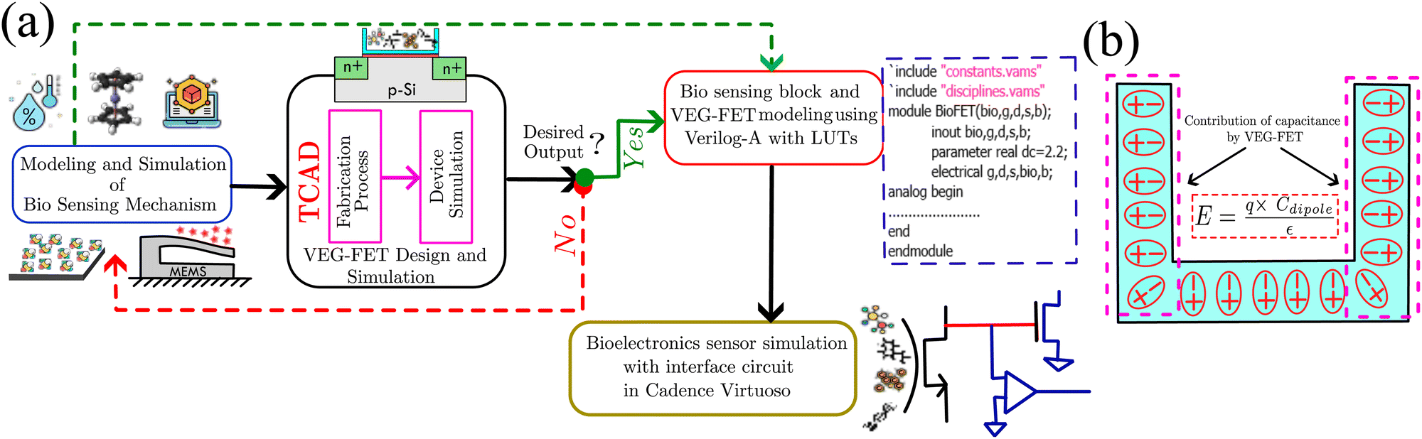
This paper addresses two key challenges in MOSFET-based gas sensors. First, a comprehensive simulation framework is developed to address challenges across multiple domains, using a look-up-table (LUT) approach, as illustrated in Fig. 1(a). The model builds upon a well-established analytical framework for the kinetics of steady polyatomic gas flow in adsorption–desorption phenomena, incorporating a flux-balanced model at the solid surface of the functionalized gate. It also considered chemical reactions at the surface and the formation of dipoles at the gate–oxide interface. The gas sensing results are integrated into the VEG-FET architecture, followed by device design and simulations using the LUT formed in Verilog-A.42 Ultimately, the entire biosensor system, including read-out electronics, is simulated to develop a fully functional bioelectronics platform.
 |
| | Fig. 1 (a) Modeling and simulation flow chart for complete biosensor system with read-out circuit. (b) Equivalent capacitor model for VEG-FET gas sensor showing the dipoles at the Pt–SiO2 interface. | |
Second, to overcome limitations of traditional MOSFET-based sensors, we propose a novel vertically extended-gate FET (VEG-FET) architecture. This design improves dipole capacitance by increasing the effective surface area of the functional gate (platinum) while maintaining a reduced channel length to enhance sensitivity, as shown in Fig. 1(b). The combination of a shorter channel and an expanded adsorption layer results in significantly improved sensitivity and a lower detection limit. However, increasing the vertical gate length is challenging, mainly due to limitations in achieving higher thickness at low temperatures. The polymer Parylene-C is suitable for offering stability against any chemical or humidity. The Parylene-C was deposited using the chemical vapor deposition (CVD) process at room temperature (RT), which is advantageous for the MOSFET-based sensor development as deposition at RT doesn't alter the material properties or doping profile beneath it.43,44 The Parylene-C can be modeled in TCAD as a new user-defined material.
2 Solid–gas interaction analysis and modeling
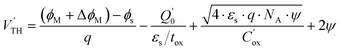
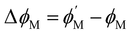
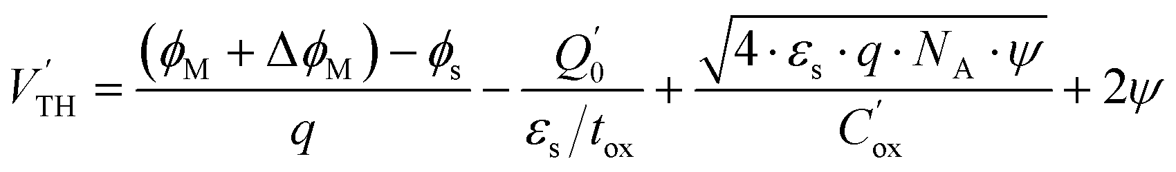
FET-based gas sensors operate by detecting interactions between gas molecules and a metal surface. When gas molecules are adsorbed onto the metal, attractive forces loosen their atomic bonds, causing the gas to dissociate into ions. These ions create a dipole moment that induces a small signal variation at the gate, changing the electric field in the channel. This change causes a shift in the work function, which changes the threshold voltage and modulates the device current. The threshold voltage of an n-MOSFET fabricated on a p-type silicon wafer substrate, accounting for the shift in metal work function due to the formation of a dipole layer at the gate surface, can be expressed as follows:45| |  | (1) |
| |  | (2) |
| |  | (3) |
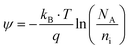
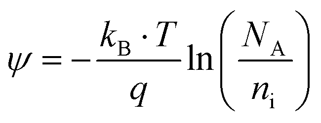
where, ϕM and ϕs are the metal and semiconductor work function, q is charge and  is the effective interface charge per unit area.
  is the oxide capacitance per unit area and NA and ni are the doping and intrinsic concentration.
From eqn (2), it is evident that ϕM is the sole parameter capable of inducing a shift in the threshold voltage. In fact, other parameters remain independent of the adsorption process, relying solely on the inherent material characteristics and the absolute temperature.
| |  | (4) |
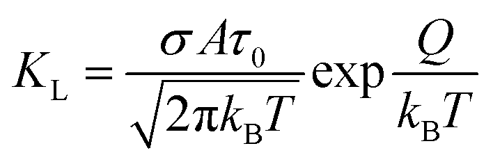
According to Langmuir theory, the phenomena of adsorption and desorption are influenced by several parameters, including the surface area (A), the partial pressure of the gas (P), the heat of adsorption (Q), probability of a molecule to be adsorbed upon hitting free space σ, and the residence time constant (τ0).46 An increase in surface area leads to a corresponding rise in fractional coverage, resulting in a greater number of adsorbed molecules at the surface and, consequently, a more significant shift in the threshold voltage VTH. The Langmuir isotherm equation defines the fractional surface coverage θ as follows:47
| |  | (5) |
where the Langmuir constant
KL is calculated as follows:
47| | 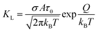 | (6) |
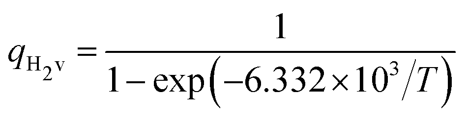
According to chemical kinetics, the reactions occurring at the surface of platinum (Pt) and their corresponding rate constants can be described in terms of enthalpy ΔH and various partition functions. Specifically, the fractional surface coverage can be expressed in terms of the vibrational partition function of occupied surface adsorption sites at the Pt–SiO2 interface, q(s′–H)v, as well as the translational qH2T, vibrational qH2v, electronic qH2E, and rotational qH2R partition functions. This relationship can be formulated as follows:45
| |  | (7) |
where
kB and
T are Boltzmann constant and temperature respectively.
α is a fitting parameter. Using
eqn (5),
(6) and
(7), the product of probability and residence time can be calculated. From
eqn (5) and
(6), the impact of gate surface area can be considered to deduce the fractional coverage
θ. It is important to note that the reported chemical kinetics model does not account for the effect of surface area, while the Langmuir model of kinetics does not incorporate the translational, vibrational, electronic, and rotational partition functions of the gas. By equating both models, a relationship that integrates surface area, partial pressure of the gas, temperature, enthalpy, partition functions, probability, and residence time has been established.
| |  | (8) |
| |  | (9) |
| | | qH2T = 5.37856 × 1026·T3/2 | (10) |
| |  | (12) |
The fractional coverage can also be expressed as the ratio of the change in metal work function to the maximum change in metal work function. Mathematically, this relationship can be represented as follows:
| |  | (14) |
Electrical measurements for the reported device were conducted under dark conditions in a vacuum at room temperature. The measurements revealed a maximum shift in threshold voltage of 1.66 V.45 This study also assumes that a similar change in threshold voltage occurs under the same fabrication processes, conditions, and material selections. The primary focus of this paper is to establish a relationship between the two aforementioned models, propose a new device architecture, and derive expressions for sensitivity and potential circuit applications.
The sensitivity of a FET based gas sensor expressed in terms of the shift in threshold voltage can be mathematically described as follows:
| |  | (15) |
The analytical model has been validated with the reported experimental data in Fig. 2(a). The maximum mismatch between the analytical and experimental results is 6.7% and the root mean square (RMS) value of the fitting is 0.013. Using the derived model for the proposed VEG-FET, θ/(1 − θ) versus is shown in Fig. 2(b) with consideration of an areal change in the device. The probability of finding a site for adsorbance on the surface and the residence time constant are prime parameters of gas kinetics with respect to gas pressure
  and are depicted in Fig. 2(c). The model is derived to predict the change in work function of the functionalised metal (Pt) with respect to gas pressure
  as shown in Fig. 2(d), which ultimately modulates the device's threshold value.
 |
| | Fig. 2 (a) Experimental and analytical results reported for θ/(1 − θ) versus with 6.75 × 10⁻⁵ m2 gate area.45 (b) Deduced analytical results for proposed VEG-FET θ/(1 − θ) versus with 6.75 × 10⁻⁵ m2 gate area.45 (b) Deduced analytical results for proposed VEG-FET θ/(1 − θ) versus with 7 × 10⁻⁵ m2 gate area. (c) Derived probability and time constant product with respect to different with 7 × 10⁻⁵ m2 gate area. (c) Derived probability and time constant product with respect to different  . (d) Change in work function with respect to applied . (d) Change in work function with respect to applied  gas pressure. gas pressure. | |
3 VEG-FET design and simulation
The drain current in a MOSFET increases with the decrease in channel length. However, scaling of channel length reduces the area which reduces the available sites for hydrogen (H2) reaction and ultimately reduces the sensitivity of the MOSFET as a gas sensor. Increasing width can mitigate this challenge. However, it increases the sensor footprint. Hence, in a vertically extended gate FET (VEG-FET), the gate electrode is extended vertically to accommodate more surface area for the H2 gas molecule reaction with the Pt layer. The schematic of the VEG-FET is shown in Fig. 3(a). The channel length (L) and width (W) are chosen as 500 μm and 100 mm respectively. A fingered VEG-FET is shown in Fig. 3(b). The fingered VEG-FET helps to accommodate larger width and reduce the resistance where each finger width is 1 mm and the number of fingers (n) is 100. The parameters of the VEG-FET are listed in Table 1. The total length of the gate electrode is Lg = L + 2 × Lh, where Lh is the extension height of the gate electrode and the net area of the gate electrode is Ag = W × Lg. The threshold voltage (VTH) varies with the incoming H2 gas pressure (PH2) (as explained in Section 2), which modulates the saturation drain current (ISatD) of the VEG-FET as follows:| |  | (16) |
where, μn and Cox are the mobility of the electron in the channel and gate capacitance, respectively. The μn and Cox remain constant and do not vary with the H2 gas reaction with the Pt gate electrode.
 |
| | Fig. 3 (a) Vertically extended gate FET (VEG-FET). (b) Isometric view of VEG-FET array. (c)–(i) VEG-FET design process flow in TCAD: (c) p-Si substrate, (d) thermal oxidation to grow 10 nm SiO2, (e) 200 nm polysilicon deposited and patterned, (f) n+ source and drain formation by ion-implantation, (g) source and drain Al metal contact formation, (h) deposition and patterning of 10 μm Parylene-C, (i) platinum (Pt) sensing vertically extended gate electrode formation. (j) Designed VEG-FET in SPROCESS. | |
Table 1 Sensor design parameters, gas kinetic coefficients and material constraints
| Parameter |
Symbol |
Value |
| Molar mass |
m (H2) |
2 g mol−1 |
| Boltzmann constant |
k
B
|
1.38 × 10⁻²³ |
| Metal work function |
ϕ
M (platinum) |
5.65 eV |
| Gibbs free energy |
ΔH (eV) |
0.202 eV |
| Fitting parameter |
α
|
107 |
| Temperature |
T
|
300 K |
| Electron charge |
q
|
1.60 × 10⁻¹⁹ C |
| Oxide thickness |
t
ox (SiO2) |
10 nm |
| Permittivity (silicon) |
ε
s
|
11.9 |
| Permittivity (SiO2) |
ε
ox
|
3.9 |
| Doping |
N
A
|
1 × 1017 cm−3 |
The VEG-FET is designed by following the standard self-aligned CMOS process flow in Sentaurus Process TCAD.48,49 A boron doped p-type silicon (p-Si) substrate with 1 × 1017 cm−3 doping concentration is selected (Fig. 3(c)) and RCA cleaned prior to dry oxidation at 900 °C to grow 10 nm of silicon dioxide (SiO2) (Fig. 3(d)). Further, 200 nm of polysilicon is deposited and patterned (Fig. 3(e)) followed by arsenic ion-implantation with a dose of 5 × 1014 cm−2 at an energy of 65 keV (Fig. 3(f)). After formation of the n+ source and drain, the polysilicon is etched completely followed by a source and drain aluminum (Al) contact electrode (Fig. 3(g)). The vertical extension of the gate electrode can be realized by deposition of a passivation layer with a thicker dimension. The Parylene-C polymer is a suitable candidate to serve as the passivation layer due to its inertness towards any chemical reaction and it is unaffected by humidity and temperature variation. Also, it is possible to deposit a thicker layer of nearly 10 μm at room temperature. In TCAD, a user defined insulating material Parylene-C is defined with a dielectric constant of 2.95. The parylene is patterned from the channel area using an AZ-4620 photoresist and oxygen (O2) plasma (Fig. 3(h)). A lift-off process can be used to realize the platinum (Pt) gate electrode. The photoresist can be deposited, followed by patterning the photoresist from the gate area, followed by 100 nm platinum (Pt) sensing layer deposition by DC sputtering. The sample should then be placed in acetone for 3–4 hours to remove the photoresists together with platinum from the unwanted regions and to realize the structure shown in Fig. 3(i). However, Parylene-C has poor adhesion with the metal layer, which may result in the peel-off of platinum from the side walls of the parylene. Hence, an adhesion treatment for Parylene-C using Silane A-174 solution is required before the lift-off process. In (Fig. 3(j)), the VEG-FET is shown after carrying out the above steps (Fig. 3(c)–(i)) in Sentaurus SProcess TCAD.
The designed device is simulated in Sentaurus Device TCAD.50 VEG-FET is a long channel device and hence, a drift–diffusion model is used to model the carrier transport in the channel accurately. Carrier scattering and velocity saturation effects are predicted by invoking the Caughey–Thomas model and the doping-dependent mobility model proposed by Arora et al.51 The Shockley–Read–Hall (SRH) recombination model and Slotboom models accounted for carrier generation and recombination and band gap narrowing effects, respectively.
The transfer characteristic curve (IDS–VGS) of the VEG-FET for different hydrogen gas pressures (PH2) is illustrated in Fig. 4(a). The VTH at different PH2 is extracted from the IDS–VGS plot. The VTH at zero PH2 is 1.15 V and reduced to 0.3 V at PH2 = 0.5 torr. The analytical solution for the change in threshold voltage (ΔVTH), from section 2, is compared with the simulation results in Fig. 4(b), and the analytical model closely matches the simulation results.
 |
| | Fig. 4 (a) IDS–VGS curve of VEG-FET at VDS = 0.1 V at PH2 = 0 to 0.5 torr in steps of 0.05 torr. (b) Analytical and simulated change in threshold voltage (ΔVTH) at different PH2. (c) IDS–VDS curve of VEG-FET at VGS = 3 V at PH2 = 0 to 0.5 torr in steps of 0.05 torr. (d) Change in drain current (ΔIDS) and relative sensitivity  at different PH2. at different PH2. | |
The output characteristic curve (IDS–VDS) of the VEG-FET at VGS = 3 V is depicted in Fig. 4(c). The drain current (IDS) increases with increasing gas pressure as VTH decreases. There is a saturation drain voltage shift observed from the IDS–VDS curve. At PH2 = 0 torr, the obtained IDS is 150 mA which increases to 310 mA at 0.5 torr as illustrated in Fig. 4(d). The relative sensitivity of the VEG-FET is ∼100% for a PH2 of 0.5 torr. The simulations are also carried out for different gate electrode extension heights (hg) to examine the effect of hg on threshold voltage (VTH) and output drain current (IDS). However, there was no significant change observed in IDS and VTH.
4 VEG-FET based H2 biosensor
A table with the Pt gate electrode work function corresponding to different hydrogen gas pressures (PH2) is prepared. A separate table is formed with all the drain current (IDS) values for the respective work function change. Gas sensing and VEG-FET components are created in Cadence Virtuoso by using Verilog-A. A VEG-FET-based common source amplifier with resistive load (RL) is designed as depicted in Fig. 5(a). The output voltage (Vout) of the sensor is:where RL is the load resistance and VDD is the power supply. The VEG-FET is worked in saturation mode throughout the sensing operation and, accordingly, the VDD is fixed at 5 V and the RL is calculated. The RL is found by considering the maximum drain current and the voltage drop across the RL is limited to ≥(VGS − VTH). In Fig. 5(b), the Vout is obtained at different hydrogen gas pressures (PH2) for different load resistances (RL). The Vout is varied from 4.20 to 3.45 V for 0 to 0.5 torr hydrogen gas pressure (PH2) at RL = 5 Ω. The Vout reduces from its zero PH2 value and lowers further with increasing PH2. The Vout is reduced with increasing RL, whereas change in output voltage (ΔVout) increases. The ΔVout = 0.74 V at RL = 5 Ω and increased to 1.3 V at 10 Ω as depicted in Fig. 5(c). The transient simulation result is shown in Fig. 5(d). The Vout varied by 24.45% at 0.1 torr PH2 and 37.8% at 0.5 torr. The interface read-out electronics can be modified further according to the application area.
 |
| | Fig. 5 (a) VEG-FET-based common source amplifier with resistive load. (b) Output voltage (Vout) at different PH2 for RL varying from 5 to 9 Ω. (c) Change in output voltage (ΔVout) at different PH2 for RL varying from 5 to 9 Ω. (d) Transient analysis of CS-amplifier, the relative sensitivity (in %) =  is varied by ∼40%. is varied by ∼40%. | |
In Table 2, the proposed VEG-FET hydrogen (H2) gas sensor is compared with other FET-type H2 sensors. The VEG-FET sensor fabrication process is in line with CMOS technology and simple without any need for specific modified materials like SnO2 nanoparticles on graphene.38 The proposed sensor works at room temperature and doesn't need microheaters.34 The operating voltage of the VEG-FET is only 3 V, which is low compared to other FET-based hydrogen gas sensors.32,34,35,38 Also, complete FET-based gas sensor system modeling and simulation are presented for the first time, considering all the parameters from different domains.
Table 2 Comparison of different FET-based hydrogen (H2) gas sensors
| Architecture |
Sensing material |
Sensing temperaturea (°C) |
Supply voltageb (V) |
Remarks |
|
RT: room temperature.
It is estimated as ≥max (VDS, VGS) at which measurements were done.
|
| TFT32 |
Pd/IGZO |
RT |
7 |
• High operating voltage. |
| • Reliability issue as channel was exposed to environment. |
| • CMOS compatibility challenge. |
| • Only TFT behavior modelled. |
| |
| SGFET28 |
Pd on MEMS ring flexure |
RT |
3 |
• Complex fabrication process. |
| • Special MEMS structure requirement. |
| • Analysis and modeling complexity. |
| • Reliability issue due to air-gap between gate and channel. |
| |
| Dual FET34 |
Graphene decorated Pd–Ag alloy nanoparticles |
250 |
4.5 |
• No device model and simulation available. |
| • High temperature requirement (microheater required). |
| |
| Nanobelt FET35 |
SnO2 |
135 |
30 |
• High temperature requirement. |
| • Only gas interaction with sensing layer modeled. |
| • High operating voltage required. |
| • Reliability issue as channel was exposed to environment. |
| |
| Graphene FET38 |
Metal oxide nanoparticle (SnO2) decorated graphene |
50 |
80 |
• High temperature requirement. |
| • Only gas interaction with sensing layer modeled. |
| • High operating voltage required. |
| • Reliability issue as channel was exposed to environment. |
| |
| VEG-FET (this work) |
Platinum |
RT |
3 |
• Simple fabrication process and CMOS compatible. |
| • Low operating voltage and temperature. |
| • Complete gas sensor system modeled considering gas interaction, MOSFET, and interface electronics. |
5 Conclusion
A MOSFET-based bioelectronics system modeling and simulation approach is presented using a hydrogen (H2) gas sensor application. The paper discussed the challenges in MOSFET-based gas sensors and presented a VEG-FET architecture that improved the hydrogen gas adsorption area which ultimately increased the change in work function of the platinum (Pt) gate electrode. The VEG-FET H2 gas sensor is designed and simulated for 0 to 0.5 torr pressure. The vertically extended Pt gate is achieved by depositing Pt isotropically over a channel in the Parylene-C polymer material which provides excellent passivation and adequate height of 10 μm. The drain current is varied from 160 mA to 308 mA for 0 to 0.5 torr PH2 at VGS = 3 V i.e. current varied by 92%. A LUT approach was followed to simulate a resistive load common source amplifier with VEG-FET considering all the design parameters. The Vout was 3.4 V without H2 gas incoming and changed to 2.10 V for PH2 = 0.5 torr at RL = 10 Ω. A simple fabrication process in line with state-of-the-art CMOS technology makes the VEG-FET based H2 sensor cost effective. The simulation and modeling approach reduces the development time. Hence, the proposed work is suitable for future bioelectronics systems with higher sensitivity.
Data availability
All data for the results of this study are directly available in the manuscript. Additional data are available from the corresponding author upon request.
Conflicts of interest
There are no conflicts to declare.
Acknowledgements
The authors acknowledge the Department of Avionics, Indian Institute of Space Science and Technology (IIST), Department of Space, Thiruvananthapuram for support in carrying out this research.
References
- H.-Y. Li, S.-N. Zhao, S.-Q. Zang and J. Li, Chem. Soc. Rev., 2020, 49, 6364–6401 RSC.
- V. S. Bhati, M. Kumar and R. Banerjee, J. Mater. Chem. C, 2021, 9, 8776–8808 RSC.
- J. Lee, Y. Jung, S.-H. Sung, G. Lee, J. Kim, J. Seong, Y.-S. Shim, S. C. Jun and S. Jeon, J. Mater. Chem. A, 2021, 9, 1159–1167 RSC.
- X. Zhou, Z. Xue, X. Chen, C. Huang, W. Bai, Z. Lu and T. Wang, J. Mater. Chem. B, 2020, 8, 3231–3248 RSC.
- T. N. Nguyen and C.-T. Dinh, Chem. Soc. Rev., 2020, 49, 7488–7504 RSC.
- M.-M. Dong, H. He, M.-W. Zhao, C.-K. Wang and X.-X. Fu, J. Mater. Chem. A, 2024, 12, 26951–26961 RSC.
- P. Huangfu and R. Atkinson, Environ. Int., 2020, 144, 105998 CrossRef CAS PubMed.
- P. Escobedo, M. Fernández-Ramos, N. López-Ruiz, O. Moyano-Rodríguez, A. Martínez-Olmos, I. Pérez de Vargas-Sansalvador, M. Carvajal, L. Capitán-Vallvey and A. Palma, Nat. Commun., 2022, 13, 72 CrossRef CAS PubMed.
- P. Kapuścik, D. Wojcieszak, P. Pokora, E. Mańkowska, J. Domaradzki, M. Mazur, P. Mazur, J. Kosto, C. Morales and M. Kot,
et al.
, Sens. Actuators, B, 2024, 417, 136148 CrossRef.
- M. Khatib and H. Haick, ACS Nano, 2022, 16, 7080–7115 CrossRef CAS PubMed.
- S. M. Majhi, A. Mirzaei, H. W. Kim, S. S. Kim and T. W. Kim, Nano Energy, 2021, 79, 105369 CrossRef CAS PubMed.
- S. Dhall, B. Mehta, A. Tyagi and K. Sood, Sens. Int., 2021, 2, 100116 CrossRef.
- M. I. A. Asri, M. N. Hasan, M. R. A. Fuaad, Y. M. Yunos and M. S. M. Ali, IEEE Sens. J., 2021, 21, 18381–18397 CAS.
- S. Hong, M. Wu, Y. Hong, Y. Jeong, G. Jung, W. Shin, J. Park, D. Kim, D. Jang and J.-H. Lee, Sens. Actuators, B, 2021, 330, 129240 CrossRef CAS.
- A. Kumar, Mater. Sci. Semicond. Process., 2020, 120, 105274 CrossRef CAS.
- J. Hodgkinson and R. P. Tatam, Meas. Sci. Technol., 2013, 24, 012004 CrossRef CAS.
- R. Ghosh, IEEE Sens. Lett., 2023, 7, 2000804 Search PubMed.
- V. C. Nguyen, H.-Y. Cha and H. Kim, Sensors, 2023, 23, 3465 CrossRef CAS PubMed.
- P. Cao, Z. Yang, S. Navale, S. Han, X. Liu, W. Liu, Y. Lu, F. Stadler and D. Zhu, Sens. Actuators, B, 2019, 298, 126850 CrossRef CAS.
- H. Bai, H. Guo, J. Wang, Y. Dong, B. Liu, Z. Xie, F. Guo, D. Chen, R. Zhang and Y. Zheng, Sens. Actuators, B, 2021, 337, 129783 CrossRef CAS.
- R. Kumar, N. Goel, D. K. Jarwal, Y. Hu, J. Zhang and M. Kumar, J. Mater. Chem. C, 2023, 11, 774–801 RSC.
- R. K. Paul, S. Badhulika, N. M. Saucedo and A. Mulchandani, Anal. Chem., 2012, 84, 8171–8178 CrossRef CAS PubMed.
- R. Sha, S. K. Puttapati, V. V. Srikanth and S. Badhulika, J. Electroanal. Chem., 2017, 785, 26–32 CrossRef CAS.
- Shrisha, C.-M. Wu, K. G. Motora, G.-Y. Chen, D.-H. Kuo and N. S. Gultom, Mater. Sci. Eng., B, 2023, 289, 116285 CrossRef CAS.
- V. Galstyan, A. Moumen, G. W. Kumarage and E. Comini, Sens. Actuators, B, 2022, 357, 131466 CrossRef CAS.
- L. Zhang, J. Dong and F. Ding, Chem. Rev., 2021, 121, 6321–6372 CrossRef CAS PubMed.
- B. Sharma, A. Sharma and J.-S. Kim, Sens. Actuators, B, 2018, 262, 758–770 CrossRef CAS.
- J. Zacharias, P. Martha and V. Seena, Micromachines, 2023, 14, 944 CrossRef PubMed.
- P. Martha, N. Kadayinti and V. Seena, IEEE Trans. Electron Devices, 2021, 68, 5133–5141 CAS.
- S. Santra, A. De Luca, S. Bhaumik, S. Ali, F. Udrea, J. Gardner, S. Ray and P. Guha, RSC Adv., 2015, 5, 47609–47616 RSC.
- P. Martha, K. Ganga, A. Sebastian, V. Seena and N. Kadayinti, IEEE Sens. J., 2022, 22, 21550–21560 Search PubMed.
- Y. T. Lee, J. Lee, H. Hwang, H. Jung, W. Lee, H. Bae and S. Im, Sens. Actuators, B, 2015, 209, 490–495 CrossRef CAS.
- W. Shin, G. Jung, S. Hong, Y. Jeong, J. Park, D. Kim, D. Jang, D. Kwon, J.-H. Bae, B.-G. Park and J.-H. Lee, Nanoscale, 2020, 12, 19768–19775 RSC.
- B. Sharma and J.-S. Kim, Sci. Rep., 2018, 8, 5902 CrossRef PubMed.
- Y. Cheng, R. Yang, J.-P. Zheng, Z. L. Wang and P. Xiong, Mater. Chem. Phys., 2012, 137, 372–380 CrossRef CAS.
- Ž. Janićijević, T.-A. Nguyen-Le and L. Baraban, Next Nanotechnol., 2023, 3–4, 100025 CrossRef.
- M. G. Bardon, H. P. Neves, R. Puers and C. Van Hoof, IEEE Trans. Electron Devices, 2010, 57, 804–813 CAS.
- Z. Zhang, X. Zou, L. Xu, L. Liao, W. Liu, J. Ho, X. Xiao, C. Jiang and J. Li, Nanoscale, 2015, 7, 10078–10084 RSC.
- S. Li, M. Zhang and H. Wang, Sci. Rep., 2021, 11, 17158 CrossRef CAS PubMed.
- V. Kumar, S. Darshan, B. Shivaraj, M. Krishna and C. Manjunatha,
et al.
, ECS Trans., 2022, 107, 5867 CrossRef.
- S. Acharyya, S. Nag, S. Kimbahune, A. Ghose, A. Pal and P. K. Guha, ACS Sens., 2021, 6, 2218–2224 CrossRef CAS PubMed.
-
P. Martha, A. Sebastian, V. Seena and N. Kadayinti, 2021 IEEE International Symposium on Inertial Sensors and Systems (INERTIAL), 2021, pp. 1–2.
- H. Park, J. Kwon, H. Ahn and S. Jung, J. Mater. Chem. C, 2019, 7, 6251–6256 RSC.
- J. Song, Y. Han and H. Yoo, J. Mater. Chem. C, 2024, 12, 12106–12114 RSC.
- M. Safari, M. Gholizadeh and A. Salehi, Sens. Actuators, B, 2009, 141, 1–6 CrossRef.
- H. Swenson and N. P. Stadie, Langmuir, 2019, 35, 5409–5426 CrossRef CAS PubMed.
- R. Brancher, S. Stefanov, I. Graur and A. Frezzotti, Vacuum, 2020, 174, 109166 CrossRef CAS.
-
User Manual, Sentaurus Process/Device Version G-2012.06, Synopsys, 2012 Search PubMed.
-
Sentaurus User’s Manual, Synopsys Inc., CA, USA, 2016 Search PubMed.
-
TCAD Sentaurus, Sdevice User Guide, ver G-2012.06, Synopsys, 2012 Search PubMed.
-
N. Arora, Mosfet modeling for VLSI simulation: theory and practice, World Scientific, 2007 Search PubMed.
|
| This journal is © The Royal Society of Chemistry 2025 |
Click here to see how this site uses Cookies. View our privacy policy here. 
 *d
*d
 is the effective interface charge per unit area.
  is the oxide capacitance per unit area and NA and ni are the doping and intrinsic concentration.


 is shown in Fig. 2(b) with consideration of an areal change in the device. The probability of finding a site for adsorbance on the surface and the residence time constant are prime parameters of gas kinetics with respect to gas pressure
  and are depicted in Fig. 2(c). The model is derived to predict the change in work function of the functionalised metal (Pt) with respect to gas pressure
  as shown in Fig. 2(d), which ultimately modulates the device's threshold value.
 with 6.75 × 10⁻⁵ m2 gate area.45 (b) Deduced analytical results for proposed VEG-FET θ/(1 − θ) versus
 with 7 × 10⁻⁵ m2 gate area. (c) Derived probability and time constant product with respect to different
  . (d) Change in work function with respect to applied
  gas pressure.


 at different PH2.
 is varied by ∼40%.