
Surface-enhanced Raman spectroscopy with single cell manipulation by microfluidic dielectrophoresis†
Kwanhwi
Ko
 a,
Hajun
Yoo
a,
Sangheon
Han
b,
Won Seok
Chang
b and
Donghyun
Kim
*ac
a,
Hajun
Yoo
a,
Sangheon
Han
b,
Won Seok
Chang
b and
Donghyun
Kim
*ac
aSchool of Electrical & Electronic Engineering, Yonsei University, Seoul, 03722, South Korea. E-mail: kimd@yonsei.ac.kr
bDepartment of Neurosurgery and Brain Research Institute, Yonsei University College of Medicine, Seoul, 03722, South Korea
cDepartment of Biomedical Engineering, The Chinese University of Hong Kong, Shatin, N.T., Hong Kong
First published on 16th October 2024
Abstract
When exposed to an alternating current (AC) electric field, a polarized microparticle is moved by the interaction between the voltage-induced dipoles and the AC electric field under dielectrophoresis (DEP). The DEP force is widely used for manipulation of microparticles in diverse practical applications such as 3D manipulation, sorting, transfer, and separation of various particles such as living cells. In this study, we propose the integration of surface-enhanced Raman spectroscopy (SERS), an extremely sensitive and versatile technique based on the Raman scattering of molecules supported by nanostructured materials, with DEP using a microfluidic device. The microfluidic device combines microelectrodes with gold nanohole arrays to characterize the electrophysiological and biochemical properties of biological cells. The movement of particles, which varies depending on the electrical properties such as conductivity and permittivity of particles, can be manipulated by the cross-frequency change. For proof of concept, Raman spectroscopy using the DEP–SERS integration was performed for polystyrene beads and biological cells and resulted in an improved signal-to-noise ratio by determining the direction of the DEP force applied to the cells with respect to the applied AC power and collecting them on the nanohole arrays. The result illustrates the potential of the concept for simultaneously examining the electrical and biochemical properties of diverse chemical and biological microparticles in the microfluidic environment.
Introduction
It has been almost 100 years since the discovery of the Raman effect by C. V. Raman in the late 1920s, a breakthrough that earned him the Nobel Prize in Physics in 1930. The Raman effect is the change in the wavelength of light, which was once referred to as the secondary radiation at degraded frequency by Raman,1 that occurs when it is scattered by molecules, resulting in a shift that provides insights into the molecular structure and composition of the substance. The spectroscopic properties of the Raman effect or Raman spectroscopy have drawn tremendous yet growing attention in recent years for various applications, i.e., early detection and diagnosis of cancer and neurodegenerative diseases,2,3 phase and crystallinity studies,4,5 molecular structure analysis,6 real-time monitoring of chemical reactions and processes,7 analysis of pharmaceutical compounds,8 non-invasive imaging of biological samples,9 monitoring and detection of environmental pollutants and contaminants,10 investigation of the properties and behaviour of nanomaterials, such as carbon nanotubes and graphene,11,12 and identification of pigments and materials used in artworks and historical artifacts.13,14 To improve the sensitivity and resolution of traditional Raman acquisition, numerous studies have been conducted on various methods including surface-enhanced Raman spectroscopy (SERS).6,10,15–17 Owing to its ultra-high sensitivity and selectivity, SERS has a vast array of applications in surface and interface chemistry,18,19 catalysis,20 nanotechnology,21 biology,22 biomedicine23 and other areas.24–26Many techniques have been proposed to further improve SERS, among which dielectrophoresis (DEP) has seen widespread use as a label-free method for real-time cell analysis. DEP takes advantage of a force exerted on dielectric particles subjected to a non-uniform electric field, which causes the particles to polarize and move. DEP devices are useful in cell sorting and manipulation as a result of subtle changes in DEP properties depending on the cell type, size, and surrounding conditions and can be a tool for cell-based assays and cell-on-a-chip devices.27–29 The DEP response is one of the important factors with which we can study the electrical properties of cells.30 When a living cell is exposed to an alternating current (AC) electric field, dipoles are created inside the cell. The interaction between the voltage-induced dipoles and the AC electric field generates force, which moves the polarized cell under DEP. If the cell is approximated as a spherical particle, the time-averaged DEP force is then given by
| FDEP = 2πr3εmRe[K(ω)]∇|Erms|2. | (1) |
Here, r denotes the cell radius, εm represents the real part of the ambient medium permittivity, Erms is the root mean-square electric field, and K(ω) is the Clausius–Mossotti factor as a measure of polarizability of the cell and is given by a ratio of complex permittivities, i.e., 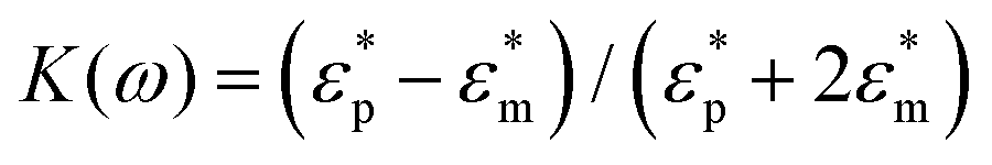 , where
  and
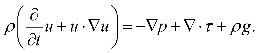
and  are the complex particle and medium permittivity, respectively. The orientation of cell behaviour as a function of the applied field is controlled by Re[K(ω)], which relates to the frequency-dependent dielectric polarization of cells in relation to the surrounding medium.31 In addition to the FDEP of eqn (1), Brownian motion and hydrodynamic force may affect the behaviour of particles suspended in a liquid medium, which may be governed by the Cauchy momentum equation of the fluid-particle system:
 | (2) |
In eqn (2), ρ denotes the fluid density, p is the pressure, τ and g represent the stress deviator tensor and the gravitational acceleration, respectively, and u is the fluid velocity that is governed by the hydrodynamic, electrostatic, and Brownian forces acting on the particles in the fluid-particle system. The effect of Brownian motion arising from random thermal fluctuations can be more significant for smaller particles, while the particle-to-particle interaction may be ignored when the inter-particle distance is large.32
Considering various factors discussed in conjunction with eqn (1) and (2), cellular behaviour can be easily controlled by varying the frequency of the AC electric field. This simplicity has driven widespread use of DEP force in the manipulation of living cells in diverse practical applications such as single cell manipulation,33 cell characterization34 and cell separation.35
In this study, we explore an integrated DEP–SERS system to characterize the electrophysiological and biochemical properties of biological cells using a microfluidic device combining microelectrodes with gold nanohole arrays. Early attempts to integrate DEP with SERS emerged in the early 2000s,36 which began to explore how DEP can be used to manipulate and concentrate particles, including biological cells and nanoparticles, for SERS analysis. There have been advancements in the 2010s in microfluidic devices, enabling the combination of DEP and SERS in compact, efficient platforms as well as the improvement in the achieved performance.37 The microfluidic systems allowed precise control over particle manipulation, facilitating applications in detecting low-abundance biomarkers and single-cell analysis.38,39 Studies integrating DEP with SERS have focused on nanoscale targets, including nanowires,40 nanoparticles,41,42 or nanowires combined with plasmonic nanoparticles.43 This approach was applied to various biological and biomolecular targets, such as proteins,44 peptides,45 bacteria,37,46,47 yeast cells,48 and fentanyl-laced heroin,49 often coated with metallic nanoparticles.
Here, we investigate the use of nanostructures for high SERS sensitivity while optimizing DEP conditions for improved particle manipulation. The changes in the SERS signals of particles were measured on gold nanohole arrays by directly manipulating microscale polystyrene (PS) beads and human brain glioblastoma cells (U-87 MG). The use of DEP in this approach allows enhanced and stable detection performance of SERS without target labelling with nanoparticles. The movement of target particles was controlled by an AC electric field applied to the gold interdigitated electrodes (IDEs) containing the nanohole arrays for direct and flexible manipulation.
Materials and methods
Optical set-up for acquisition of Raman signals
The optical set-up that we used for measurement is presented in Fig. 1(a), which shows a system for the acquisition and collection of Raman signals and manipulation via DEP force. The set-up includes a DEP trapping chip fabricated through a lift-off process. For experimentation, an inverted microscope (IX-73, Olympus, Tokyo, Japan) equipped with an objective (Olympus UPLFLN 60× objective, NA 0.90, Olympus) was used. Raman spectra were resonantly excited by a 532 nm laser source (Cobolt Samba™, 532 nm, HÜBNER, Kassel, Germany). A spectrometer (QE Pro Raman+, Ocean Optics, Orlando, FL, USA) was employed to capture Raman signatures from target cells during Raman spectrum measurements. A notch filter (NF533-17, Thorlabs, Newton, NJ, USA) was employed to eliminate Rayleigh scattered light during Raman signal acquisition. The photograph of the constructed DEP–SERS system and the optical instrument is presented in Fig. 1(b).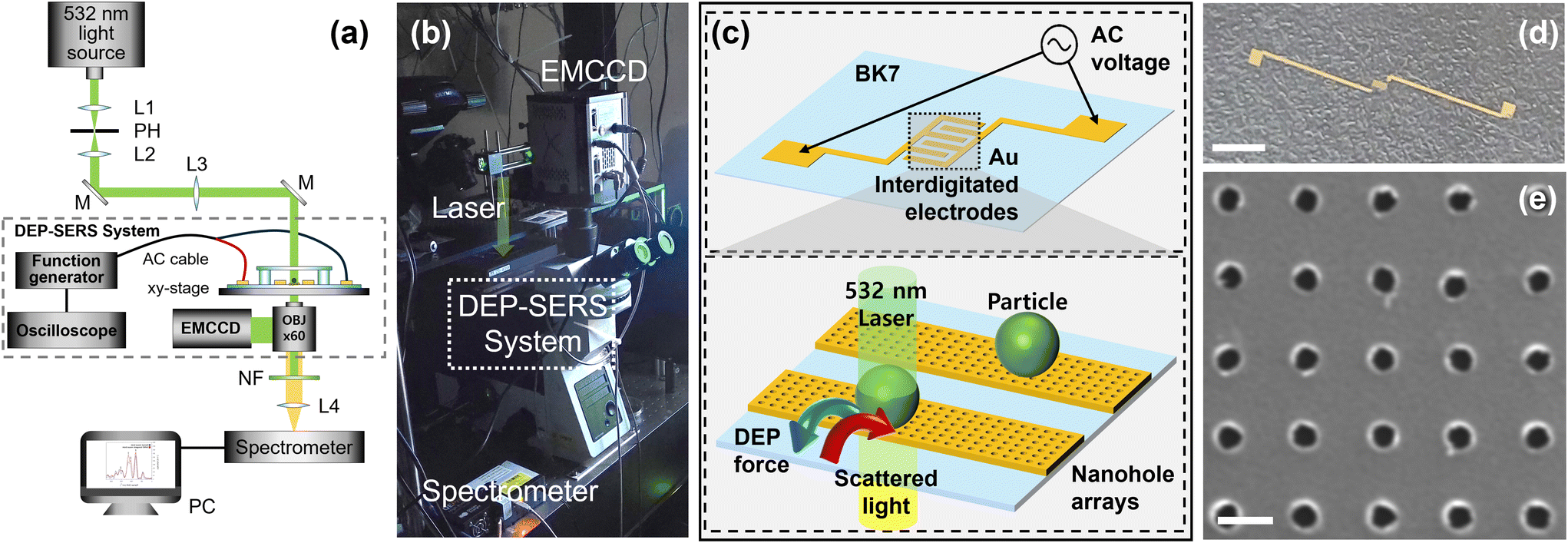 | ||
| Fig. 1 (a) Schematic representation of the optical set-up (M: mirrors, L1–L4: lenses, PH: pinhole, OBJ: objective lens, NF: notch filter, and light source λ = 532 nm). (b) Photograph of the constructed DEP–SERS system. (c) Schematic representations of a DEP–SERS chip. (d) Photograph of a DEP–SERS chip (scale bar: 4 mm). (e) SEM image of fabricated nanohole arrays (diameter: 250 nm and period: 700 nm, scale bar: 500 nm). | ||
Data processing of acquired signals
Acquired signals were analyzed using Python 3.8 and OriginPro 8.5 (OriginLab, Northampton, MA, USA). Data pre-processing and cosmic ray removal were performed using custom-built scripts based on the Open Raman Processing Library.50 Subsequent processing consisted of baseline correction, signal smoothing, and graph fitting of the spectra conducted using OriginPro 8.5. Experimental noise was removed by the Savitzky–Golay smoothing with a window width of 5 spectral data points.51Sample fabrication
To fabricate a microfluidic DEP–SERS device, a positive PMMA electron-beam resist was initially coated on a glass substrate with a thickness of 270 nm. Subsequently, nanohole arrays with a height of 20 nm were patterned by electron-beam lithography and the lift-off process. This is followed by defining electrodes used for DEP with a thickness of 100 nm. The nanohole array was patterned with 250 nm diameter and 700 nm period approximately. Schematic representations of a DEP–SERS chip with interdigitated metal electrodes with the photograph are provided in Fig. 1(c) and (d). When an AC power supply is applied to both ends of the electrode, an electric field is generated at the IDE at the center of the chip, which gives rise to the formation of a net DEP force field due to the Maxwell–Wagner interfacial polarization in a field gradient. The IDE consists of gold electrodes with a width of 25 μm, separated by a 25 μm gap. Depending on the frequency of the AC power, the direction of the DEP force trapping particles on the electrode with the nanohole arrays changes, allowing particles to be positioned above the nanoholes or to be released. A SEM image of nanohole arrays fabricated on the gold electrode is presented in Fig. 1(e).Numerical calculation
Electromagnetic simulations were performed using a three-dimensional finite-difference time-domain (FDTD) solver to calculate the near-field distribution formed by gold nanohole arrays with periodic boundary conditions. The refractive indices of gold and the BK7 glass substrate were obtained from Palik.52 The refractive index of water was set to 1.333. The grid size of meshes was set to 5 nm. In addition, the DEP behaviour of particles in the microfluidic flow system was determined by simulating the electric field and DEP forces for the IDE chip structure used in the experiment using the finite-element method.Cell culture and sample preparation
For biological validation, we have used U-87 MG cells that are a human glioblastoma cell line often used in brain cancer research. The U-87 MG cell-line was purchased from the American Type Culture Collection (ATCC®, HTB-14™). Cells were cultured under a humidified atmosphere at 37 °C, maintaining 5% carbon dioxide in the incubator. The culture medium consisted of Dulbecco's Modified Eagle's Medium (DMEM, Sigma Aldrich), supplemented with 10% fetal bovine serum (FBS, Gibco) and 1% penicillin–streptomycin (Gibco). To detach adherent cells from the culture dish, the cells were rinsed with Phosphate Buffer Solution (PBS, pH 7.4, Gibco) and subsequently treated with 0.25% trypsin–EDTA solution (Sigma Aldrich) for 3 minutes in the incubator. The cells detached from the culture dish using trypsin were washed three times with PBS and transferred to the DEP experiment buffer consisting of 8.6% (w/w) sucrose (Sigma Aldrich), 0.3% (w/w) D-glucose (Sigma Aldrich), 0.20% (v/v) PBS, and 1.0 mg mL−1 bovine serum albumin (BSA, Sigma-Aldrich) by centrifugation.53 The conductivity of the DEP experiment buffer was 60 μS cm−1.Results and discussion
Numerical results
SERS is associated with the near-fields due to the nanohole arrays. The near-field distribution of electromagnetic waves formed by the gold nanohole arrays was simulated using FDTD with periodic boundary conditions. The model consists of a nanohole (diameter: ∅) with 100 nm thickness in the BK7 glass substrate. Calculations were performed for the cross-sections along the x-, y-, and z-axes, as illustrated in Fig. 2(a). We assumed normal incidence of light that was linearly polarized along the x-axis with λ = 532 nm. Fig. 2(b–d) present the electric field amplitudes |E| in the cross-sections of the x-, y-, and z-axes for ∅ = 250 nm. Given that a linearly polarized light source along the x-axis was used, the calculation indicates stronger signal enhancement in the cross-section along the x-axis, as shown in Fig. 2(b), compared to the one in the cross-section along the y-axis shown in Fig. 2(c). Fig. 2(d) shows the electric field distribution in the horizontal cross-section, which was obtained in the water medium 10 nm above the top surface of the nanohole arrays. For nanoholes of varying sizes, the fields tend to be more localized with a smaller nanohole when compared to those with diameter ∅ = 150 nm, 200 nm, and 300 nm presented in Fig. 2(e), (f), and (g). ESI S1† provides more detailed information regarding the effect of nanohole diameter. In contrast, the peak electric field amplitude does not display a significant or monotonic change. The size of a nanohole is on the order of wavelength; therefore field localization predominantly occurs near the edges of the nanohole, which is consistent with earlier studies using mesoscopic nanostructures.54–59 Because the strength of Raman signals is proportionate with |E|4 to the first degree, it is suggested that the acquisition of Raman signals may be more localized than shown in Fig. 2(b–d). Smooth electrodes or nanohole arrays out of resonance with the excitation source may reduce the near-field enhancement and weaken SERS signals.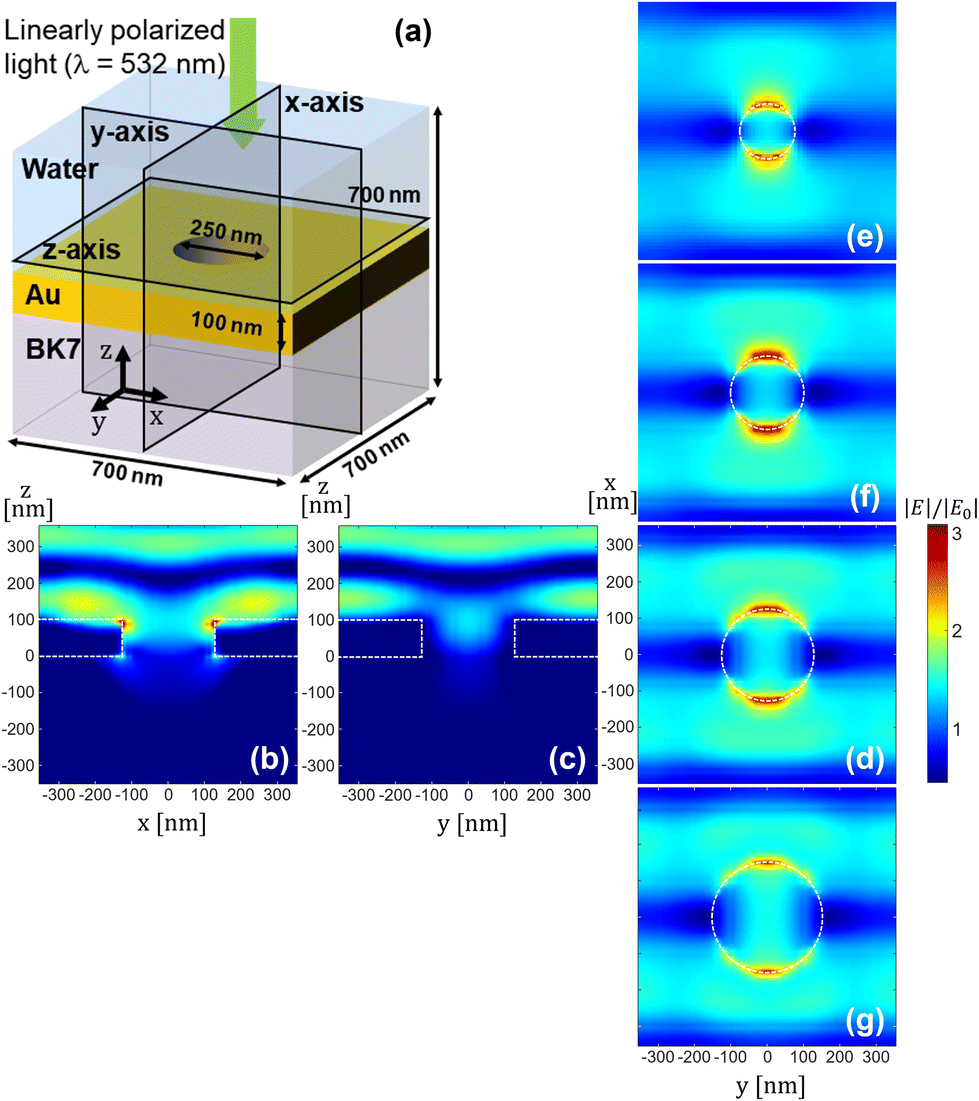 | ||
| Fig. 2 (a) 3D schematic representations of the FDTD model of a gold nanohole (period: 700 nm and thickness: 100 nm) on top of the glass substrate in water medium. (b–d) FDTD simulation results of the gold nanohole structure with a nanohole diameter ∅ = 250 nm in the cross-sections of the x-, y-, and z-axes shown in (a). Near-field distribution with the nanohole diameter being varied to: (e) ∅ = 150 nm, (f) 200 nm, and (g) 300 nm. The electric field amplitudes |E| represented by the color bar were normalized by the incident electric field amplitude E0; thus the color bar scale is unitless. The color bar applies to (b–g). The results confirm the localization and enhancement of electric fields by a nanohole, especially at edges, which can be used for SERS. | ||
To simulate the DEP field, we first calculated the distribution of the AC electric field generated by the IDE electrodes, as presented in Fig. 3(a). The 25 μm gold electrodes, spaced 25 μm apart, create a non-uniform electric field, and the resulting DEP force is indicated by the arrows in Fig. 3(b). Calculations were performed using a spherical single-shell model with a diameter of 10 μm. As mentioned in the Materials and methods section, the cell samples for the DEP experiments were treated with trypsin to create a suspension in the buffer, making the spherical cell modeling suitable for experimental calculations. According to the calculations, the DEP force causes cells on the electrodes as well as those in the gap regions to be drawn towards the substrate surface. The DEP force causes cells to become fully trapped in the nanoholes on the electrode surface, allowing for a controllable SERS effect. Additionally, it was observed that the particles experience the strongest force at the edges of the electrodes, suggesting that measurements in the DEP–SERS system using the IDE chip should be performed at the edges rather than at the center for optimal results.
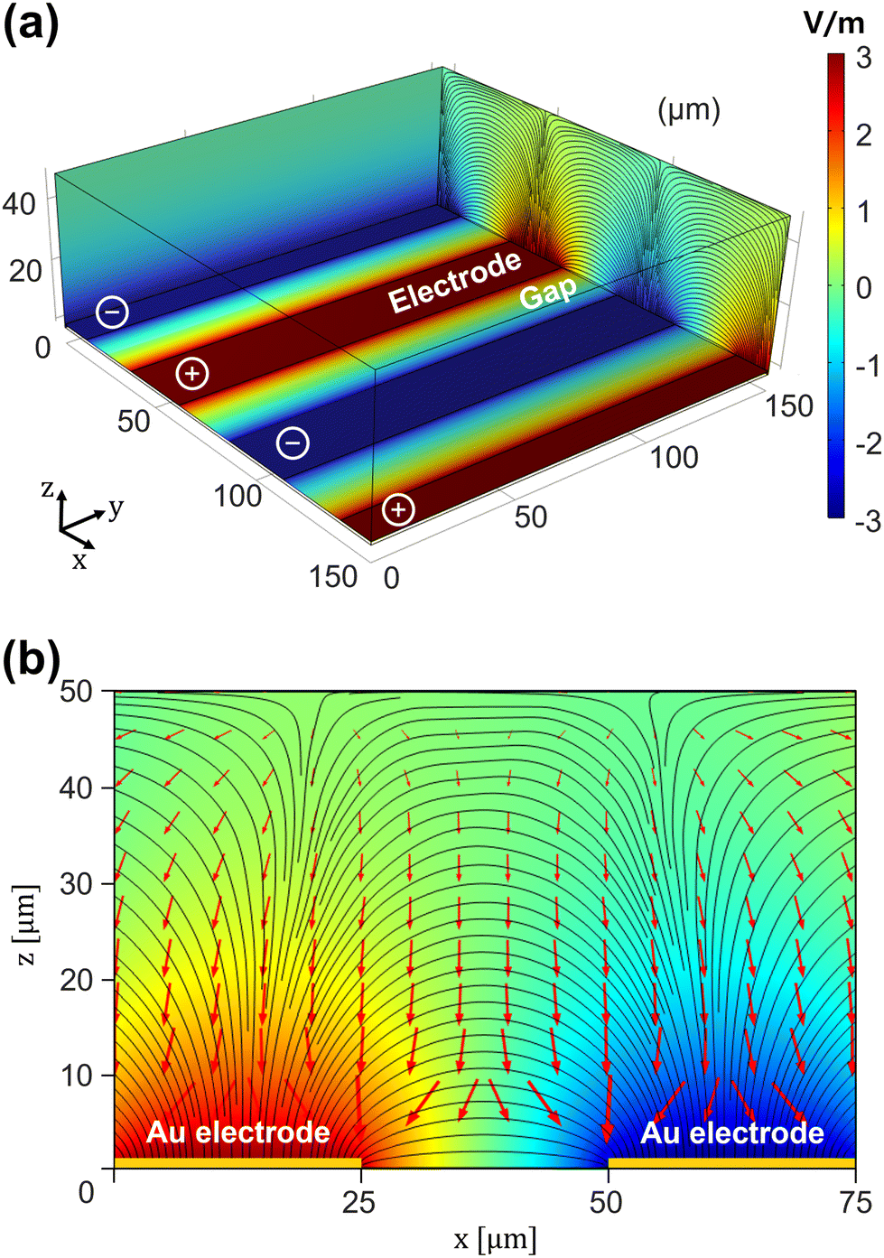 | ||
| Fig. 3 (a) Simulation of the electric field generated by IDEs composed of gold, with each electrode having a width of 25 μm and separated by a 25 μm gap. (b) Cross-sectional view along the x-axis of the electric field and DEP force vectors. The arrows indicate the direction of the positive DEP force vectors acting on a cell with a diameter of 10 μm. | ||
Acquisition of Raman signals from PS beads
The DEP set-up allows measurement of Raman signals on a single bead at a desired location. For the test, we used a PS bead (diameter ∅ = 10 μm) diluted in DI water, which may be trapped by the non-uniform electric field induced by gold electrodes. For the DEP trapping of a PS bead, an AC power supply with a voltage of 2Vpp at a frequency ranging from 1 kHz to 10 kHz was applied to the surrounding electrodes. The polarization frequency associated with IDEs, which can vary depending on other structural parameters, is estimated to be below 1 kHz, while DEP may dominate other fluidic force components in our system.60–64 A PS bead was moved from the positive DEP (p-DEP) trapping position above the nanohole array, where the Raman signal is measured, to the negative DEP (n-DEP) trapping position due to the change in the direction of the DEP force with varying frequency. The movement is shown in the bright and dark field optical image of a trapped PS bead presented in Fig. 4(a). To verify the passage of incident light through a single bead trapped by the DEP force, scattered images were captured without a notch filter, as shown in Fig. 4(b).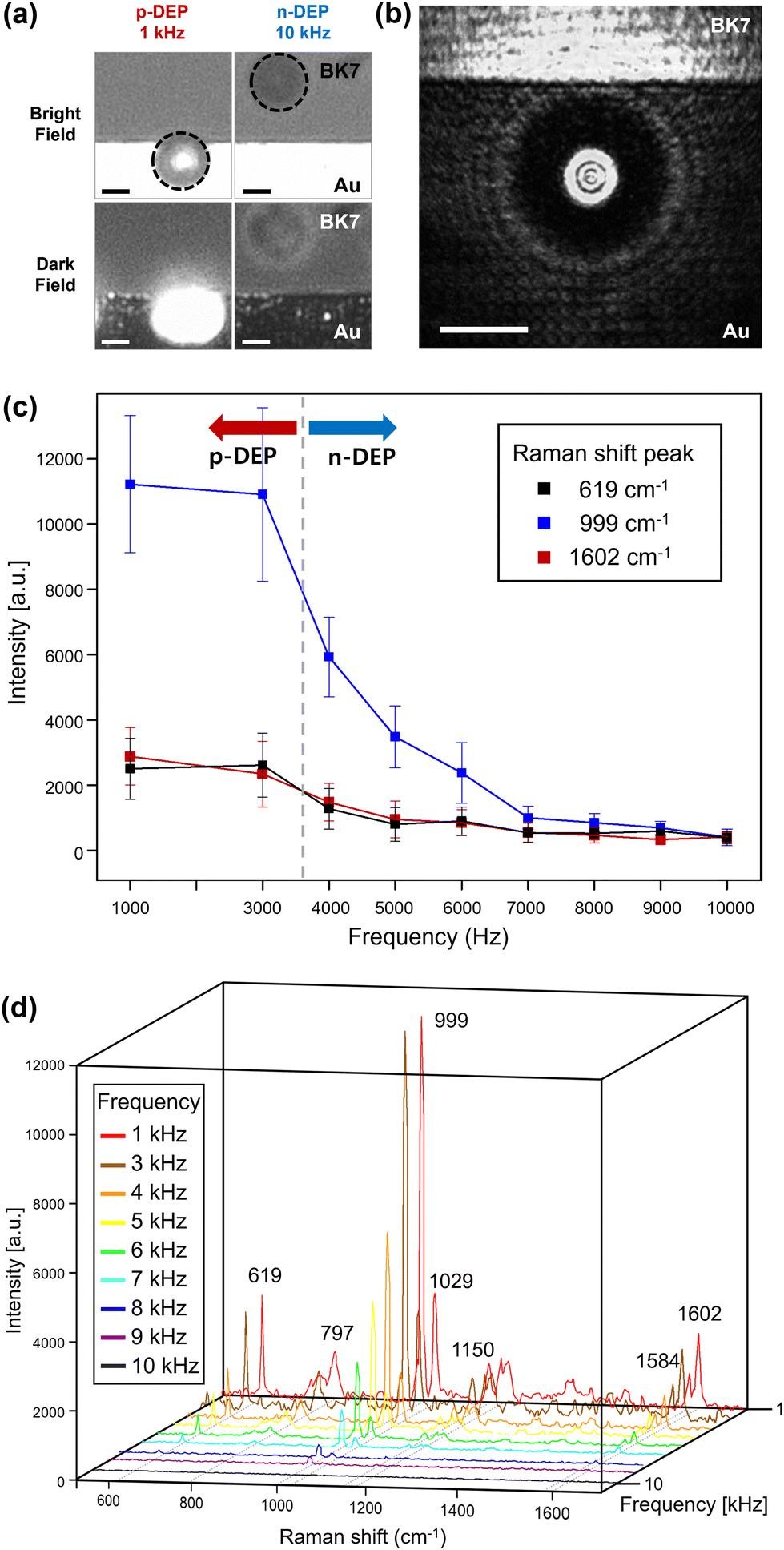 | ||
| Fig. 4 (a) An optical image of a trapped PS bead (diameter: 10 μm) in the bright-field and the dark-field (scale bar: 5 μm) captured for the electrode with nanohole arrays and the BK7 glass substrate. (b) Scatter image of a positive trapped PS bead (scale bar: 5 μm). (c) Raman peak intensity of a PS bead on gold nanohole arrays at different DEP frequencies (n = 10). (d) Raman spectra of a PS bead recorded on gold nanohole arrays at different DEP frequencies. The frequency decreases along the z-axis from 10 to 1 kHz. | ||
A trapped bead emits Raman signals upon exposure to the light localized by nanohole arrays in the near-field. The variation in the average signal intensity of the main Raman peaks at 619, 999, and 1602 cm−1 from 10 measurements with respect to the frequency changes is presented in Fig. 4(c). As the applied frequency of the electrode increases from 1 kHz to 10 kHz, a decrease in the average intensity can be observed. Of particular interest is the sharp decrease in SERS intensity that begins between 3 kHz and 4 kHz. Thus, it can be suggested that the crossover frequency, at which the DEP force reverses the direction, should be between 3 kHz and 4 kHz for the PS bead under test. This is consistent with the known crossover frequency of 3.8 kHz for 10 μm PS beads, shown as the vertical dashed line in Fig. 4(c).65 The SERS data of PS beads, measured at fixed positions on the gold nanohole array as a function of frequency, are shown in Fig. 4(d). The obtained results closely match the known Raman bands of PS.66,67 For reference, the assignment of each Raman peak is summarized in Table 1.
| Peak (cm−1) | Assignment |
|---|---|
| 619 | Ring deformation mode |
| 797 | C–H out-of-plane deformation |
| 999 | Ring breathing mode |
| 1029 | C–H in-plane deformation |
| 1150 | C–C stretch |
| 1584 | C![[double bond, length as m-dash]](https://www.rsc.org/images/entities/char_e001.gif) C stretch C stretch |
| 1602 | Ring-skeletal stretch |
Raman signals of control and manipulated U-87 MG cells
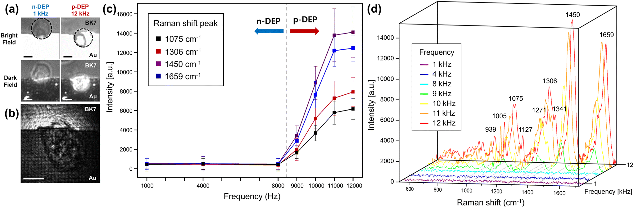
Enhancement of Raman signals was evaluated by measuring U-87 cells in the absence of the DEP field on a gold film and the BK7 glass substrate, in comparison with those on gold nanohole arrays patterned on the film at a frequency of 12 kHz with a voltage of 2Vpp. Raman signals acquired on gold nanohole arrays and the BK7 glass substrate confirm surface-enhanced field enhancement, i.e., at 1450 cm−1, the SNR was found to be 24.0 dB on gold nanohole arrays vs. 15.9 dB on the BK7 substrate, based on the first standard deviation. This indicates that an enhancement of 8.1 dB can be associated with SERS due to the nanohole arrays (see ESI S2† for more details).Fig. 5(a) shows an optical image of a U-87 MG cell trapped at different positions of the DEP chip at an applied frequency. At frequencies of 1 kHz and 12 kHz with a voltage of 2Vpp, the cell experiences negative DEP (n-DEP) and positive DEP (p-DEP) traps, respectively. To confirm light transmission through a single trapped cell via DEP force, scatter images were acquired using an EMCCD, as depicted in Fig. 5(b). Following a protocol similar to the PS bead experiments, we measured SERS signals by increasing the frequency applied to the electrodes of the DEP–SERS chip with U-87 MG cells from 1 kHz to 12 kHz. We compared the average intensities of the four strongest Raman peaks (1075, 1306, 1450, and 1659 cm−1) from 10 measurements and presented them in Fig. 5(c). An increase in the intensity was observed between 8 kHz and 9 kHz, implying the presence of crossover in the case of U-87 MG cells in this range, which is shown as the vertical dashed line. This result aligns well with those reported in the literature regarding the DEP characteristics of biological cells in an experimental buffer under the same conductivity.34Fig. 5(d) illustrates the variation in the Raman spectra measured for a single cell with changing frequency. The spectral regions with peaks of SERS signals were observed at around 1005 cm−1 (phenylalanine), 1075 cm−1 (protein), 1306 cm−1 (lipid), 1341 cm−1 (DNA), 1450 cm−1 (fatty acids), and 1659 cm−1 (protein). These peak assignments of Raman spectra are well established and support the reliability of our data through comparison with the literature.68–70 The Raman peak assignments of U-87 MG cells are summarized in Table 2.
 | ||
| Fig. 5 (a) An optical image of a trapped U-87 MG cell in the bright-field and the dark-field (scale bar: 5 μm) captured for the electrode with nanohole arrays and the BK7 glass substrate. (b) Scatter image of a positive trapped U-87 MG cell (scale bar: 5 μm). (c) Raman peak intensity of a U-87 MG cell placed on gold nanohole arrays at different DEP frequencies (n = 10). (d) Raman spectra of a U-87 MG cell on gold nanohole arrays at different DEP frequencies. The frequency increases along the z-axis from 1 to 12 kHz. | ||
| Peak (cm−1) | Assignment |
|---|---|
| 939 | Protein |
| 1005 | Phenylalanine |
| 1075 | Protein |
| 1127 | Protein |
| 1271 | Protein |
| 1306 | Lipid |
| 1341 | DNA |
| 1450 | Fatty acids |
| 1659 | Protein |
Discussion
The results presented in Fig. 4 and 5 suggest that DEP can be used to move target objects for increasing measurable Raman signals, which in this case were enhanced by SERS based on metallic nanohole arrays. The SERS signal variations of PS beads and U-87 MG cells with respect to the frequency changes exhibit opposite trends. This phenomenon, well-documented in the literature on the DEP behaviour of artificial particles and biological cells, is attributed to the differences in the dielectric properties and conductivity between the beads (single homogeneous material) and biological cells (two or more layers).71,72 If we define the improved efficiency of SERS following manipulation by DEP, ESERS, as the peak SERS intensity with respect to the background, ESERS = 26.5 (at the Raman shift/999 cm−1) and 30.8 (1450 cm−1), respectively, for the detection of PS beads and U-87 MG cells. The improvement by more than an order of magnitude, which is represented by ESERS, is a direct result of exact positioning of target particles enabled by DEP and shows that such capability can be critical for high performance detection in the microfluidic environment.Concluding remarks
In this study, we investigated the Raman signal acquisition and properties of PS beads and U-87 MG cells using a DEP–SERS system integrated with a nanostructured microfluidic chip platform. By manipulating PS beads and U-87 MG cells with DEP, which is similar to controlling a target on an xy-stage, we measured the corresponding changes in SERS signals on the nanohole array. Beyond Raman peak analysis, we estimated the crossover frequencies, revealing key electrical properties of the particles, e.g., the DEP behaviour of PS beads and biological cells was found to be opposite. With DEP, we were able to come up with significantly enhanced SERS efficiency. Our study demonstrates the practical applicability and potential of this system for simultaneously studying the electrical and biochemical properties of various chemical and biological microparticles. In future studies, multiple cell types can be detected for potential diagnostic applications.Author contributions
Kwanhwi Ko: conceptualization, formal analysis, investigation, methodology, software, visualization, writing – original draft and writing – review & editing. Hajun Yoo: investigation, software, validation, visualization, writing – original draft and writing – review & editing. Sangheon Han: resources and writing – original draft. Won Seok Chang: funding acquisition, resources and writing – original draft. Donghyun Kim: conceptualization, formal analysis, funding acquisition, project administration, supervision, writing – original draft and writing – review & editing.Data availability
The data used for this article will be provided upon request to the authors.Conflicts of interest
The authors declare no conflicts of interest.Acknowledgements
This work was supported by the National Research Foundation (NRF) grants funded by the Korean Government (NRF-2022R1A4A2000748) and the Korea Medical Device Development Fund (Project number: RS-2020-KD000103).References
- C. V. Raman and K. S. Krishnan, Nature, 1928, 121, 501–502 Search PubMed.
- H. Lui, J. Zhao, D. McLean and H. Zeng, Cancer Res., 2012, 72, 2491–2500 CrossRef PubMed.
- K. Ko, Y. Seo, S. Im, H. Lee, J. Y. Park, W. S. Chang and D. Kim, Korean J. Opt. Photonics, 2022, 33, 331–337 Search PubMed.
- T. T. Thu Nguyen, Y. Kim, S. Bae, M. Bari, H. R. Jung, W. Jo, Y.-H. Kim, Z.-G. Ye and S. Yoon, J. Phys. Chem. Lett., 2020, 11, 3773–3781 CrossRef PubMed.
- A. Z. Samuel, M. Zhou, M. Ando, R. Mueller, T. Liebert, T. Heinze and H.-O. Hamaguchi, Anal. Chem., 2016, 88, 4644–4650 CrossRef CAS.
- S.-Y. Ding, J. Yi, J.-F. Li, B. Ren, D.-Y. Wu, R. Panneerselvam and Z.-Q. Tian, Nat. Rev. Mater., 2016, 1, 1–16 Search PubMed.
- S. Lukin, K. Užarević and I. Halasz, Nat. Protoc., 2021, 16, 3492–3521 CrossRef CAS PubMed.
- K. Bērziņš, S. J. Fraser-Miller and K. C. Gordon, Int. J. Pharm., 2021, 592, 120034 CrossRef.
- J. Marzi, E. Fuhrmann, E. Brauchle, V. Singer, J. Pfannstiel, I. Schmidt and H. Hartmann, ACS Appl. Mater. Interfaces, 2022, 14, 30455–30465 CrossRef CAS.
- T. T. Ong, E. W. Blanch and O. A. Jones, Sci. Total Environ., 2020, 720, 137601 CrossRef CAS PubMed.
- Y. Park, K. Hembram, R. Yoo, B. Jang, W. Lee, S.-G. Lee, J.-G. Kim, Y.-I. Kim, D. J. Moon and J.-K. Lee, J. Phys. Chem. C, 2019, 123, 14003–14009 CrossRef CAS.
- C. Neumann, S. Reichardt, P. Venezuela, M. Drögeler, L. Banszerus, M. Schmitz, K. Watanabe, T. Taniguchi, F. Mauri and B. Beschoten, Nat. Commun., 2015, 6, 8429 CrossRef CAS.
- E. P. Tomasini, C. M. F. Dubois, N. C. Little, S. A. Centeno and M. S. Maier, Microchem. J., 2015, 121, 157–162 CrossRef CAS.
- D. Chiriu, F. A. Pisu, P. C. Ricci and C. M. Carbonaro, Materials, 2020, 13, 2456 CrossRef CAS.
- C. Chen, N. Hayazawa and S. Kawata, Nat. Commun., 2014, 5, 3312 CrossRef PubMed.
- H. Lee, K. Kang, K. Mochizuki, C. Lee, K.-A. Toh, S. A. Lee, K. Fujita and D. Kim, Nano Lett., 2020, 20, 8951–8958 CrossRef CAS PubMed.
- H. Lee, H. Yoo, G. Moon, K.-A. Toh, K. Mochizuki, K. Fujita and D. Kim, J. Chem. Phys., 2021, 155 Search PubMed.
- S. Dick, M. P. Konrad, W. W. Lee, H. McCabe, J. N. McCracken, T. M. Rahman, A. Stewart, Y. Xu and S. E. Bell, Adv. Mater., 2016, 28, 5705–5711 CrossRef CAS PubMed.
- X. Jiang, D. Yin, M. Yang, J. Du, W. Wang, L. Zhang, L. Yang, X. Han and B. Zhao, Appl. Surf. Sci., 2019, 487, 938–944 CrossRef CAS.
- Y. Zhang, Z. Ye, C. Li, Q. Chen, W. Aljuhani, Y. Huang, X. Xu, C. Wu, S. E. Bell and Y. Xu, Nat. Commun., 2023, 14, 1392 CrossRef CAS PubMed.
- H.-L. Liu, K. Zhan, K. Wang and X.-H. Xia, TrAC, Trends Anal. Chem., 2023, 159, 116939 CrossRef CAS.
- D.-K. Lim and P. P. P. Kumar, Nanophotonics, 2024, 13, 1521–1534 CrossRef.
- B. Deng, Y. Zhang, G. Qiu, J. Li, L. L. Lin and J. Ye, Small, 2024, 2402235 CrossRef.
- Y. Sun, D. Lou, W. Liu, Z. Zheng and X. Chen, Adv. Opt. Mater., 2023, 11, 2201549 CrossRef.
- N. Tyagi, G. Sharma, D. Kumar, P. P. Neelratan, D. Sharma, M. Khanuja, M. K. Singh, V. Singh, A. Kaushik and S. K. Sharma, Coord. Chem. Rev., 2023, 496, 215394 CrossRef.
- L. Jiang, M. M. Hassan, S. Ali, H. Li, R. Sheng and Q. Chen, Trends Food Sci. Technol., 2021, 112, 225–240 CrossRef.
- G. Medoro, N. Manaresi, A. Leonardi, L. Altomare, M. Tartagni and R. Guerrieri, IEEE Sens. J., 2003, 3, 317–325 CrossRef.
- H. Zhang, H. Chang and P. Neuzil, Micromachines, 2019, 10, 423 CrossRef PubMed.
- M. Alshareef, N. Metrakos, E. Juarez Perez, F. Azer, F. Yang, X. Yang and G. Wang, Biomicrofluidics, 2013, 7, 011803 CrossRef PubMed.
- I. S. Park, J. Lee, G. Lee, K. Nam, T. Lee, W.-J. Chang, H. Kim, S.-Y. Lee, J. Seo and D. S. Yoon, Anal. Chem., 2015, 87, 5914–5920 Search PubMed.
- R. R. Pethig, Dielectrophoresis: Theory, Methodology and Biological Applications, John Wiley & Sons, 2017 Search PubMed.
- A. T. J. Kadaksham, P. Singh and N. Aubry, Electrophoresis, 2004, 25, 3625–3632 CrossRef PubMed.
- T. Zheng, Z. Zhang and R. Zhu, Anal. Chem., 2019, 91, 4479–4487 Search PubMed.
- S. Choi, K. Ko, J. Lim, S. H. Kim, S.-H. Woo, Y. S. Kim, J. Key, S. Y. Lee, I. S. Park and S. W. Lee, Sensors, 2018, 18, 3543 CrossRef PubMed.
- V. Varmazyari, H. Habibiyan, H. Ghafoorifard, M. Ebrahimi and S. Ghafouri-Fard, Sci. Rep., 2022, 12, 12100 CrossRef PubMed.
- I. Cheng, H.-C. Chang, D. Hou and H.-C. Chang, Biomicrofluidics, 2007, 1, 021503 Search PubMed.
- I. Cheng, C.-C. Lin, D.-Y. Lin and H.-C. Chang, Biomicrofluidics, 2010, 4, 034104 CrossRef PubMed.
- S. Cherukulappurath, S. H. Lee, A. Campos, C. L. Haynes and S.-H. Oh, Chem. Mater., 2014, 26, 2445–2452 CrossRef.
- K. J. Freedman, C. R. Crick, P. Albella, A. Barik, A. P. Ivanov, S. A. Maier, S.-H. Oh and J. B. Edel, ACS Photonics, 2016, 3, 1036–1044 CrossRef.
- T. Ge, S. Yan, L. Zhang, H. He, L. Wang, S. Li, Y. Yuan, G. Chen and Y. Huang, Nanotechnology, 2019, 30, 475202 CrossRef PubMed.
- A. F. Chrimes, A. A. Kayani, K. Khoshmanesh, P. R. Stoddart, P. Mulvaney, A. Mitchell and K. Kalantar-Zadeh, Lab Chip, 2011, 11, 921–928 RSC.
- G. B. Almeida, R. J. Poppi and J. A. F. da Silva, Analyst, 2017, 142, 375–379 RSC.
- M. Constantinou, C. Panteli, L. Potamiti, M. I. Panayiotidis, A. Agapiou, S. Christodoulou and C. Andreou, Adv. Sens. Res., 2024, 3, 2300161 CrossRef.
- S. Azimi and A. Docoslis, Sens. Actuators, B, 2023, 393, 134250 CrossRef.
- K. H. P. Vu, M.-C. Lee, G. H. Blankenburg, Y.-J. Chang, M.-L. Chu, A. Erbe, L. Lesser-Rojas, Y.-R. Chen and C.-F. Chou, Anal. Chem., 2021, 93, 16320–16329 CrossRef PubMed.
- H. Y. Lin, C. H. Huang, W. H. Hsieh, L. H. Liu, Y. C. Lin, C. C. Chu, S. T. Wang, I. T. Kuo, L. K. Chau and C. Y. Yang, Small, 2014, 10, 4700–4710 CrossRef PubMed.
- A. B. Nowicka, M. Czaplicka, T. Szymborski and A. Kamińska, Anal. Bioanal. Chem., 2021, 413, 2007–2020 CrossRef PubMed.
- A. F. Chrimes, K. Khoshmanesh, S.-Y. Tang, B. R. Wood, P. R. Stoddart, S. S. Collins, A. Mitchell and K. Kalantar-Zadeh, Biosens. Bioelectron., 2013, 49, 536–541 CrossRef.
- R. Salemmilani, M. Moskovits and C. D. Meinhart, Analyst, 2019, 144, 3080–3087 RSC.
- A. Savitzky and M. J. Golay, Anal. Chem., 1964, 36, 1627–1639 CrossRef.
- G. Sheehy, F. Picot, F. Dallaire, K. Ember, T. Nguyen, K. Petrecca, D. Trudel and F. Leblond, J. Biomed. Opt., 2023, 28, 025002–025002 Search PubMed.
- E. D. Palik, Handbook of Optical Constants of Solids, Academic press, 1998 Search PubMed.
- A. C. Sabuncu, J. A. Liu, S. J. Beebe and A. Beskok, Biomicrofluidics, 2010, 4, 021101 CrossRef.
- D. Kim, J. Opt. Soc. Am. A, 2006, 23, 2307–2314 CrossRef PubMed.
- K. Kim, S. J. Yoon and D. Kim, Opt. Express, 2006, 14, 12419–12431 Search PubMed.
- K. Kim, J. Yajima, Y. Oh, W. Lee, S. Oowada, T. Nishizaka and D. Kim, Small, 2011, 8, 892–900 CrossRef PubMed.
- W. Lee, Y. Kinosita, Y. Oh, N. Mikami, H. Yang, M. Miyata, T. Nishizaka and D. Kim, ACS Nano, 2015, 9, 10896–10908 CrossRef CAS.
- T. Son, D. Lee, C. Lee, G. Moon, G. E. Ha, H. Lee, H. Kwak, E. Cheong and D. Kim, ACS Nano, 2019, 13, 3063–3074 CrossRef CAS.
- T. Son, G. Moon, C. Lee, P. Xi and D. Kim, Nanophotonics, 2022, 11, 4805–4819 CrossRef.
- A. González, A. Ramos, N. G. Green, A. Castellanos and H. Morgan, Phys. Rev. E, 2000, 61, 4019 CrossRef.
- Z. Gagnon and H.-C. Chang, Electrophoresis, 2005, 26, 3725–3737 CrossRef CAS PubMed.
- W. Liu, Y. Ren, Y. Tao, X. Chen, B. Yao, M. Hui and L. Bai, Phys. Fluids, 2017, 29, 112002 CrossRef.
- M. Vazquez-Pinon, B. Pramanick, F. G. Ortega-Gama, V. H. Perez-Gonzalez, L. Kulinsky, M. J. Madou, H. Hwang and S. O. Martinez-Chapa, J. Micromech. Microeng., 2019, 29, 075007 CrossRef CAS.
- C. L. Song, Y. Tao, W. Y. Liu, Y. C. Chen, R. Xue, T. Y. Jiang, B. Li, H. Y. Jiang and Y. K. Ren, Phys. Rev. E, 2022, 105, 025102 CrossRef CAS PubMed.
- X. Xing, M. Zhang and L. Yobas, J. Microelectromech. Syst., 2012, 22, 363–371 Search PubMed.
- T. E. Bridges, M. P. Houlne and J. M. Harris, Anal. Chem., 2004, 76, 576–584 CrossRef CAS.
- M. Mazilu, A. C. De Luca, A. Riches, C. S. Herrington and K. Dholakia, Opt. Express, 2010, 18, 11382–11395 CrossRef CAS.
- J. Rix, O. Uckermann, K. Kirsche, G. Schackert, E. Koch, M. Kirsch and R. Galli, J. R. Soc., Interface, 2022, 19, 20220209 CrossRef CAS.
- A. R. Boccaccini, P. X. Ma and L. Liverani, Tissue Engineering Using Ceramics and Polymers, Woodhead Publishing, 2021 Search PubMed.
- M. Kopeć, A. Borek-Dorosz, K. Jarczewska, M. Barańska and H. Abramczyk, Analyst, 2024, 149, 2697–2708 RSC.
- S.-K. Fan, P.-W. Huang, T.-T. Wang and Y.-H. Peng, Lab Chip, 2008, 8, 1325–1331 RSC.
- Q. Chen and Y. J. Yuan, RSC Adv., 2019, 9, 4963–4981 RSC.
Footnote |
| † Electronic supplementary information (ESI) available. See DOI: https://doi.org/10.1039/d4an00983e |
| This journal is © The Royal Society of Chemistry 2024 |