
 Open Access Article
 This Open Access Article is licensed under a Creative Commons Attribution-Non Commercial 3.0 Unported Licence
Top-down micro and nano structuring of wide bandgap semiconductors for ultraviolet photodetection†
Ramit Kumar
Mondal
a,
You Jin
Kim
a,
Yikai
Liao
a,
Zhihua
Zheng
ab,
Jiangnan
Dai
 b and
Munho
Kim
*a
b and
Munho
Kim
*a
aSchool of Electrical and Electronic Engineering, Nanyang Technological University, 50 Nanyang Avenue, Singapore, 639798, Singapore. E-mail: munho.kim@ntu.edu.sg
bWuhan National Laboratory for Optoelectronics, Huazhong University of Science and Technology, Wuhan 430074, China
First published on 9th January 2025
Abstract
Solar blind ultraviolet (UV) photodetectors (PDs) based on III-nitrides, silicon carbide (SiC), and other wide bandgap semiconductors such as diamond and gallium oxide (Ga2O3) offer excellent device performance such as low dark current, high responsivity, high detectivity, and high UV/visible rejection ratio. The performance of the UV PDs can be further improved by implementing micro and nanostructures via enhanced light–matter interaction. This review paper primarily encompasses the detailed study and recent development of various approaches of dry and wet etching techniques to enable the formation of micro and nanostructures built on the aforementioned material systems. Applications of different etching techniques for the development of PDs have been reviewed subsequently. Finally, the major challenges and future direction of micro and nanostructured UV PDs are briefly discussed.
Introduction
At the present time, 95% of industrial production of electronic devices still relies on first-generation semiconductors i.e., Si and Ge. Second-generation semiconductors like III-arsenide and III-phosphide did not receive much attention for standard applications as they are expensive and toxic. Third-generation semiconductors like III-nitrides and silicon carbide (SiC) are being considered as a potential material over Si in many advanced electronic and photonic applications due to their high thermal conductivity, high breakdown field strength, and high saturation electron drift velocity.1 Other wide bandgap (WBG) semiconductors like diamond and gallium oxide (Ga2O3) are also attracting substantial amounts of research interest as the beyond third-generation semiconductors. Third-generation semiconductors including III-nitrides can be used to enable various modern electronics applications such as 5G/6G mobile communication,2 and electric vehicle and smartphone fast charging3,4 due to their unique properties like high temperature sustainability, high power handling capability, high frequency operability, and adaptability to other harsh conditions.5 Optoelectronics including display, sensing, and lighting are among the other prominent fields of applications for these third-generation (and beyond) semiconductors. Wider band gaps facilitate them as the perfect materials for optoelectronic devices operating in the ultraviolet (UV) wavelength region. The UV wavelength spectrum can be subdivided into UV-A (400–315 nm), UV-B (315–280 nm), UV-C (280–200 nm), and vacuum UV (200–100 nm). Numerous applications of UV optoelectronics over other wavelength bands including medical imaging apparatuses, indoor farming, communication systems, security surveillance, nanofabrication tools, astronomy, and satellite positioning have emerged over the past years.6 Especially after the outbreak of COVID-19, research on UV optoelectronics has become a topic of interest with substantial societal impacts due to their germicidal and disinfection competences. Light emitters (e.g., LEDs and laser diodes) and photodetectors (PDs) are the dominant optoelectronic devices operating in the UV wavelength region. At present, the III-nitride material system is quite mature and is industrially accepted to produce UV LEDs7,8 and solar blind UV PDs,9,10 even at the commercial level due to some beneficial factors such as band gap tunability by alloy engineering, availability of both p and n type dopants, and matured epitaxial growth techniques. In contrast, the usage of SiC, Ga2O3, and diamond is mostly limited to the construction of solar blind UV PDs due to their indirect bandgap structures. Solar blind UV PDs have been employed in many significant applications like tracking missiles, combustion flame detection, UV astronomy, satellite positioning, etc.11Light management by means of light trapping is a very important aspect to improve the performance of the PDs. In terms of PDs, their performance heavily depends on the amount of light that can be absorbed. For most photo-sensing materials, constructing PDs, surface reflection is considered as major optical loss that limits the amount of incident light being absorbed. Therefore, light management by means of implementing antireflective structures has been studied extensively and intensively to enhance light absorption and achieve further improvement in the performance of PDs.12 Two methods are typically employed to realize antireflection: layered coating and surface texturing (Fig. 1). The former one relies on the occurrence of destructive interference between the reflected light wave from the top surface and the interface of two layers with dissimilar refractive index. On the other hand, the latter one involves either microstructures or nanostructures on the surface to realize multiple light reflection and scattering for enhanced light absorption.
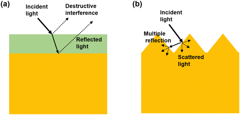 | ||
| Fig. 1 Anti-reflection strategies: (a) layered coating and (b) surface texturing. | ||
One of the main benefits of nanofabrication in UV photodetectors lies in reducing optical reflection through light-trapping structures. By texturing the device surface at micro- or nanoscale dimensions, incident photons undergo multiple reflections, thereby increasing the effective optical path and enhancing light absorption. As a result, responsivity can be significantly improved. Additionally, such surface modifications can influence carrier dynamics by altering interface states, which may affect dark current and response speed. These aspects underscore the physics behind nanofabrication as a powerful approach to boost overall device performance.
Top-down or bottom-up approaches are being adopted to fabricate micro or nanostructures.13 Due to several advantages such as precise controllability, scalability, and lower power consumption, top-down approaches are more industrially compatible. In the case of top-down approaches, various etching techniques have been explored. Fig. 2 represents the classifications of various top-down etching techniques along with schematics illustrating the fundamental mechanisms of each approach. The details of these mechanisms are discussed in subsequent sections.
 | ||
| Fig. 2 Classification of top-down etching techniques with representative schematics for each (plasma etching: typical ICP reactor configuration showing the direction of the magnetic field and chamber geometry,14 laser assisted etching: principle of laser micromachining for trench formation,15 crystal and defect dependent etching: OH− adsorption on Ga dangling bonds and subsequent back-bond attack,16 MacEtch: five-step mechanism illustrating the catalysis, injection, diffusion, etching, and by-product removal processes,17 and electro-chemical etching: experimental setup for generating porous GaN).18 | ||
A summarized comparison of these top-down etching techniques is provided in Table 1, highlighting their key advantages, drawbacks, and methods to address potential surface and material defects.
| Etching technique | Advantages | Disadvantages | Potential mitigation methods |
|---|---|---|---|
| Plasma etching | High resolution | Higher cost | Post etch annealing to heal defects |
| High aspect ratio | |||
| Controllability | Surface defects | Optimized process parameters | |
| Repeatability | |||
| Laser assisted etching | Environmental friendliness | Elevated local temperature can damage surface or introduce unwanted thermal stress | Careful selection of laser power and scan speed |
| Good controllability | |||
| Clean and less complex steps | Use of protective coatings | ||
| Crystal and defect dependent etching | Lower cost | Low aspect ratio structures | Optimized chemical concentrations and temperature |
| Fewer surface defects | Limited geometry control | Pre-patterning for selective etching | |
| MacEtch | High aspect ratio nano/microstructures | Requires noble metal catalyst patterning | Optimized metal deposition |
| Electrochemical etching | Ability to create porous structures and nanowires | Requires external bias | Uniform electrode design and bias control |
| Possible non-uniform etching | Real time monitoring |
As illustrated in Fig. 3, our review covers a comprehensive discussion on the micro/nano-structuring of gallium nitride (GaN), SiC, Ga2O3, and diamond using dry and wet etching techniques to enhance the performance of PDs via a light trapping effect. Firstly, we have discussed various etching techniques and their mechanisms. The effect of various etching parameters on the etching profile of the aforementioned semiconductors is included. In the next section, we present the device level applications of micro and nanostructures for UV PDs. Finally, we conclude this review article with the major challenges and future outlook of the nanostructured UV PDs.
 | ||
| Fig. 3 An illustration of various etching techniques for the fabrication of micro/nanostructures of III-nitrides, SiC, Ga2O3, and diamond. | ||
Process and materials
Dry etching
Dry etching is a process of removing material from a surface by means of bombardment of heavy ions and reactive gas plasma or high energy laser beam. The most prominent advantage of dry etching is that it can achieve high anisotropy which leads to higher etching rate in the vertical direction compared with that in the horizontal direction. As a result, very high-resolution and high aspect ratio nanostructures can be fabricated. Besides that, a higher degree of controllability and repeatability can be ensured by dry etching techniques. However, dry etching techniques are costlier than wet etching processes, which require complex equipment.Plasma etching
Plasma etching involves exposing the substrate to a high-speed stream of glow discharge plasma, which contains species such as heavy ions and reactive radicals. Plasma etching proceeds by either physical sputtering, chemical reaction, or a combination of both processes. Physical sputtering involves the bombardment of positive ions on the substrate surface, resulting in high-energy collisions that eject atoms from the material. Chemical reaction involves the formation of volatile products between the reactive gas and the substrate material, which are then pumped away by the vacuum system. The etching rate depends on the detachment of atoms from the surface of target materials and the volatility of product materials. However, re-deposition of non-volatile compounds can hamper the etching process. More importantly, due to heavy ion bombardment, many defects on the surface are generated at the bombarded surface, causing degraded electrical properties of the material by plasma damages. Induced defects can be recovered by annealing at appropriate temperatures.19 Four kinds of plasma etching techniques exist, namely reactive ion etching (RIE), high-density plasmas (HDP), chemically assisted ion beam etching (CAIBE), and low energy electron enhanced etching (LE4). Fig. 4 displays different micro/nano-structuring of GaN, SiC, Ga2O3, and diamond by an inductive coupled plasma (ICP)-RIE process.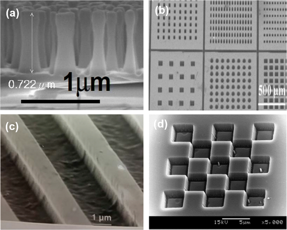 | ||
| Fig. 4 Micro/nano structuring by ICP-RIE. (a) GaN. Reproduced with permission.20 Copyright 2008, Optica. (b) SiC. Reproduced with permission.21 Copyright 2017, Springer Nature. (c) Ga2O3. Reproduced with permission.22 Copyright 2018, American Vacuum Society. (d) Diamond. Reproduced with permission.23 Copyright 2005, Elsevier. | ||
Chlorine (Cl2)-based gas chemistry is mostly adapted for plasma etching of III-nitrides. The first report of GaN RIE used SiCl4 plasma with a DC bias of 400 V to achieve an etch rate of above 50 nm min−1.24 Compared to simple RIE, ICP etching can offer fast etch rates with low damage. Though Cl2/Ar chemistry can provide satisfactory etch rates and profile for most of the GaN micron and nanostructures, the addition of BCl3 (i.e., Cl2/BCl3/Ar gas chemistry) plasma can improve sputter desorption due to higher mass ions and reduced surface oxidation which can produce more consistent results. The Ar percentage influences the etching characteristics. Higher Ar percentage increases the anisotropy due to higher physical etching but at the same time it invokes more surface damages and low etch rates.25 Apart from that, parameters including pressure, DC bias, and ICP power vastly influence the etching characteristics. The etch rate increases up to a certain gas pressure (1–2 mTorr) and it is reduced afterwards. Moreover, the anisotropy is also hampered when the pressure reaches above 10 mTorr. Due to the enhanced sputter desorption of the etch product and breaking of Ga–N bonds, the etch rate initially increases with an increase in DC bias. However, the etch rate is saturated at higher DC bias because of sputter desorption of reactive species from the surface before the reactions occur. This leads to operation under an adsorption limited etch regime. Similarly, the etch rate initially increases with ICP power but it is stabilized later, attributed by the operation under an adsorption limited etch regime. Typically, the etch rate decreases when the material changes from GaN to AlN. It is related to the bond strength, which is higher for AlN (11.52 eV per atom) as compared to GaN (8.92 eV per atom).26 High bond strength results in lower etch rate. The effect of temperature on GaN and AlN etching is not very significant. It is noteworthy to mention that the N-face GaN is etched faster with respect to Ga-face GaN under an identical condition.27
Mostly, fluorine (F2)-based gas chemistry is used over chlorine-based gas chemistry due to the higher etching rate for the plasma etching of SiC.28 In general, different kinds of F2-based gas like SF6, CF4, CHF3, C2F6, CBrF3, and NF3 are applied for etching of SiC.29–34 The F content of the gas directs the formation of C–F chemical bonds such as ionic, semi-ionic and covalent ones, which result in different etching characteristics.35 The etching characteristics depend on the degree of crystallinity of SiC. The polycrystalline SiC is etched more aggressively as compared to single crystal SiC due to the presence of a large number of dangling bonds at the grain boundaries.36 The difference between the dangling bonds at crystal faces is also responsible for the 20% higher etching rate of β-SiC compared with 6H-SiC. A smoother surface can be achieved by adding 30% of Ar to the SF6 + O2 gas mixture.37,38 The roughness of the etched surface of SiC also depends on temperature, RF power, and distance between the plasma source and sample. It has been observed that the increasing of temperature range of 100 to 300 °C can lower the root-mean-square (RMS) roughness of the surface from 153 to 0.7 nm.39 Moreover, a higher temperature of around 150 °C can raise the etch rate. The roughness of the etched surface of SiC increases with the increase in the distance between the RF source and sample as well as the RF power.40 Around 20% O2 inclusion results in an increase in etch rate due to an increase in the number of broken C–F bonds. However, above 20% of O2 inclusion results in dilution of F atoms, which slows down the etching rate.31 Although O2 inclusion results in better etch rates, it also creates trenches at the bottom of the etched surfaces. This trench formation is related to the formation of SiFxOy compound by-products during the SiC etching by SF6 and O2 plasma. During the etching process, those SiFxOy by-products are gathered at the etched surface boundary. As a result, the rate of chemical reaction at those boundaries is increased, which results in the formation of trenches.41 Another problem with inclusion of O2 plasma arises in terms of limitation of photoresist as a mask for actual device fabrication. As O2 plasma etches photoresist significantly, a hard mask needs to be used. Different metal masks as the substitutes of photoresist (mostly Ni, Cr) are generally used for deep etching of SiC.
Similar to GaN, Ga2O3 can be etched using chlorine-based gas chemistry. It was reported that the highest etch rate of 180 nm min−1 was accomplished under etching with 90 W RF power, 900 W ICP power and BCl3/Ar flow rate of 35/5 sccm.42 BCl3 plasma etching provides higher etch rates than Cl2 etching. This happens because BCl3 radicals react with the oxygen atoms in the Ga2O3. They remove oxide more efficiently which is attributed to increased Cl radical density in BCl3 with response to Cl2.43 Yang et al. observed that a higher etch rate was achieved at a RF frequency of 13.56 MHz than at 40 MHz.44 Instead of Cl2-based gas chemistry, F2-based gas chemistry can provide a more controlled etching profile, while it sacrifices etch rate.45
Potential of single crystal diamond (SCD) is highly rated for advanced electronic devices. It is difficult to etch diamond because it is a highly inert material. O2 plasma is mainly used to dry etch SCD.46,47 As a result, a hydrocarbon-based photoresist cannot be used for masking purposes. Generally, SiO2 or Al is used as a hard mask for deep etching of diamond.48,49 A two cycle process is a popular technique to etch SCD.50 In this technique, O2 is used in the first cycle to etch the SCD. In the second cycle, F2-based gas is added with O2 to remove silicon oxide residue on the diamond surface. It is found that instead of using only O2, inclusion of Ar increases the etch rate due to physical etching.51 Therefore, one cycle etching with O2/SF6/Ar followed by the next cycle etching with SF6/Ar is preferred. It is observed that Cl plasma produces better surface quality. Therefore, Ar/Cl plasma is used before Ar/O2 plasma to incorporate Cl.52 Apart from the gas chemistry, RF power, ICP power, chamber pressure, and temperature are important parameters that influence the etching characteristics. The chamber pressure, ICP and RF power are in the range of 1–15 mTorr, 500–2000 W and 200–400 W, respectively.53 Temperature has a minor effect on etching characteristics. It is noted that room temperature is ideal for SCD etching.
Laser surface texturing/etching
The laser surface texturing (LST) process has many beneficial features such as environmental friendliness, good controllability, cleanliness and less complexity. LST works upon heating and melting of the targeted material to be etched by irradiation of short pulses of a laser. Advanced LST can produce feature sizes as low as 200 nm.54 The precision of LST is subjected to pulse duration. If the pulse duration is 10−13 s, the absorbed energy cannot be transferred from electrons to the lattice in such a short relaxation time. In this case, the electron–electron interaction can only increase the local electron temperature material by the irradiated laser pulse. On the other hand, for longer pulse duration, electrons can transfer the energy to the lattice, leading to an increase in temperature locally. Due to very highly localized temperature, material expulsion from the irradiated surface takes place, leading to surface patterning. Higher localization of temperature causes clean patterning. Localization of temperature is ensured by shorter pulse width. Broadening of the temperature affected zone arising from longer pulse duration leaves enormous debris and distorted features. Thus, the quality of the textured features degrades as the laser pulse duration increases from femtosecond to nanosecond.55 Laser pulse intensity also impacts the morphology of the textures. Generally a higher energy of the pulses creates ripples in the surface due to melting of the target material in higher quantity. Fig. 5 shows different micro/nano-structuring of GaN, SiC, Ga2O3, and diamond by LST.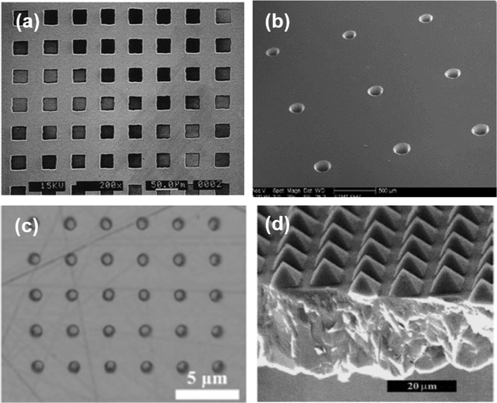 | ||
| Fig. 5 Micro/nano structuring by LST. (a) GaN. Reproduced with permission.56 Copyright 1998. Elsevier. (b) SiC. Reproduced with permission.57 Copyright 2006. Elsevier. (c) Ga2O3. Reproduced with permission.58 Copyright 2022. Elsevier. (d) Diamond. Reproduced with permission.59 Copyright 1999, Wiley-VCH. | ||
Patterning on GaN films using LST was firstly achieved by employing a Nd:YAG pulsed laser with a wavelength of 355 nm.60 The pulse duration, beam diameter, and energy density were 5 ns, 7 mm, and 420 mJ cm−2, respectively. High-energy laser pulses heat up the GaN film locally above 900 °C, resulting in a rapid effusion of nitrogen. Next the sample was chemically treated by hydrochloric acid (HCl) to remove excess gallium. The etch rate was in the range of 50–70 nm per pulse. Similarly, F2-based LST of GaN was realized to obtain an etched surface with roughness of 4 nm.61 The KrF laser was also employed for etching of GaN by ablation.62 After laser ablation, the samples were treated with HCl or H2SO4/H2O2 solution to etch out material residues such as Ga and Ga oxide. An etching rate of 60 nm per pulse was obtained under low pressure conditions. Simultaneous irradiation of F2 and KrF laser was found to be favorable towards the reduction of surface roughness of the etched GaN region.
LST of 3C, 4H, and 6H-SiC was carried out by various research groups. Cone shaped nanostructures of 6H-SiC with the dimensions of 100–200 nm height and 5–10 nm width were obtained by the nitrogen laser with a wavelength of 337 nm and a pulse duration of 7 ns.63 The required energy density for etching of 6H-SiC was determined to be 3.5 J cm−2. Laser assisted micro machining was carried out for 3C-SiC by employing a UV laser. KrF and ArF lasers, with respective emitting wavelengths of 248 nm and 193 nm, and pulse durations of 34 ns and 26 ns, were deployed to create through holes in 400 μm thick 3C-SiC.57 Ti: sapphire laser emitting system with a wavelength of 800 nm and a laser pulse duration of 40 fs was utilized to make nanostructures on 4H-SiC.64
A very limited number of literature reports on the LST of Ga2O3 are available. Zhang et al. reported on the texturing of β-Ga2O3 by using green (515 nm) and IR femtosecond lasers (1030 nm).58 The pulse duration of 285 fs and the single pulse energy of 22 nJ were set to obtain the desired morphology. They found that, for similar etched depths, the energy required for the 515 nm laser is much smaller than the 1030 nm laser. Moreover, the etching damage was also lesser in the case of lower wavelength laser.
Nanosecond pulse excimer lasers have facilitated the micro-structuring of diamond surfaces. In order to deliver nano-structuring, more advanced techniques including controlled ablation through graphitization and etching via two-photon surface excitation were utilized. Trucchi et al. reported a detailed review on laser texturing on the diamond surface.65Fig. 6 describes different parameters for laser-based texturing of diamonds.65
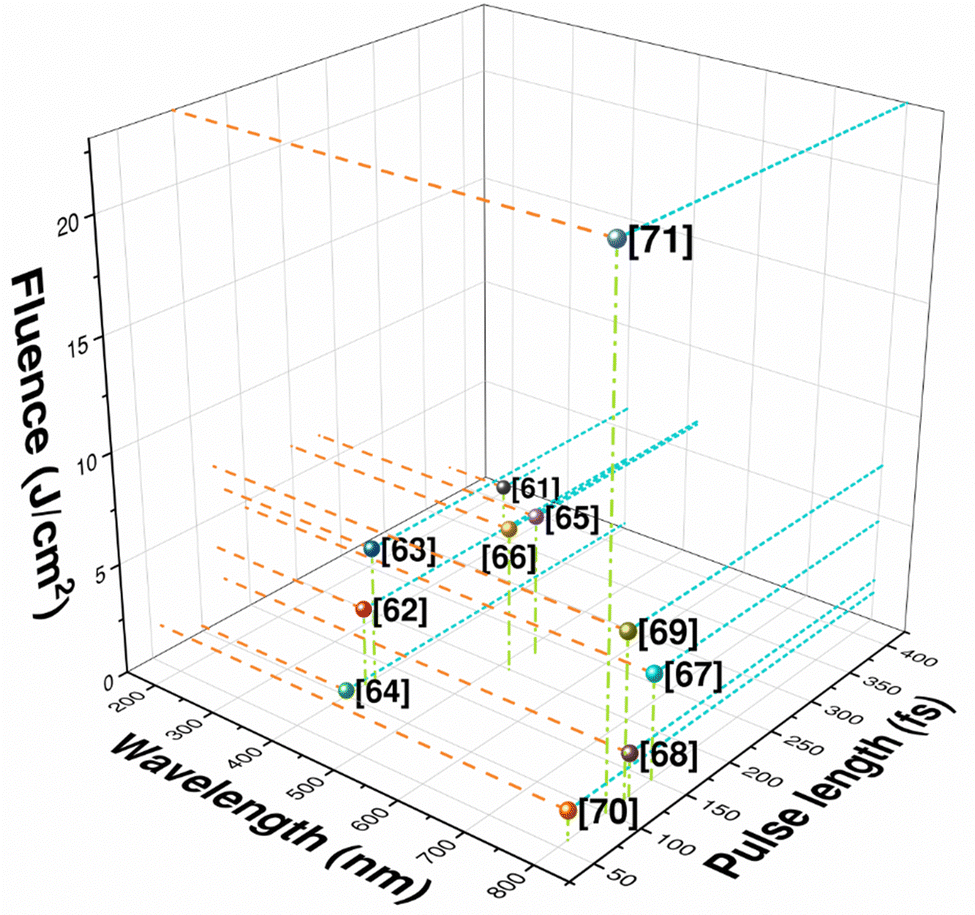 | ||
| Fig. 6 Pulse laser parameters for laser texturing of diamonds reported in different research articles.66–76 | ||
Wet etching techniques
Wet etching of a material generally proceeds in three steps. First, etchants are diffused to the surface of the material to be etched. Second, chemical reaction takes place between etchants and the exposed surface. Third, the reaction products are removed from the etched surface. A wet etching process is generally cheaper than dry etching and it also produces less surface defects. Although it is difficult to achieve anisotropic wet etching, the processes such as defect dependent wet etching, electrochemical etching, and metal-assisted chemical etching (MacEtch) can produce a higher degree of anisotropy, which can lead to the creation of high aspect ratio nanostructures.Crystal plane and defect dependent wet etching
A difference in etching rate between the undistorted matrix and defective region leads to an anisotropic etching profile. This anisotropic etching can be utilized for micro/nano-structuring of WBG semiconductors as a top-down approach.The etching characteristics of Ga-polar and N-polar GaN varied due to the different states of surface bonding arising from polarity. It was evident that N-polar GaN can be etched by KOH solution at a temperature around 80 °C, resulting in the formation of hexagonal hillocks with facets of {10![[1 with combining macron]](https://www.rsc.org/images/entities/char_0031_0304.gif) } planes stopping the etching, resulting in a pyramid shaped structure.77 It should be noted that Ga-polar GaN cannot be etched by the same etching condition. This is because of the repulsion between the OH− ion and dangling bonds of nitrogen. Similarly, thte formation of nanotip pyramids was observed by Hock et al. with KOH treatment of N-polar GaN (Fig. 7(a)).78 Conversely, defect selective etching of Ga-polar GaN can be carried out by soaking it into the hot (200 °C) phosphoric acid (H3PO4).79,80 It will selectively etch Ga-polar GaN epitaxial films along the (0001) direction to form hexagonal etch pits. The possible origins for hexagonal pit formation can be the open core screw dislocations. It was noticeable that etch pits were formed on screw or mixed dislocations, but etch pits were absent on edge dislocations. As compared to GaN, the dislocation and polarity sensitive etching is more prominent in AlN. High quality N-polar AlN can be etched in KOH based solution even at room temperature. On the other hand, the etch resistance of Al-polar AlN is much higher than the N-polar AlN when treated with KOH solution at the temperature of 80 °C.81 Molten solutions of NaOH/KOH can etch hexagonal pits on the AlN surface (Fig. 7(b)).82 The etching rate selectivity of AlN and GaN under varying solution temperatures of H3PO4 is also noticeable. The AlN etching by H3PO4 takes place at much lower temperatures as compared to GaN.83
} planes stopping the etching, resulting in a pyramid shaped structure.77 It should be noted that Ga-polar GaN cannot be etched by the same etching condition. This is because of the repulsion between the OH− ion and dangling bonds of nitrogen. Similarly, thte formation of nanotip pyramids was observed by Hock et al. with KOH treatment of N-polar GaN (Fig. 7(a)).78 Conversely, defect selective etching of Ga-polar GaN can be carried out by soaking it into the hot (200 °C) phosphoric acid (H3PO4).79,80 It will selectively etch Ga-polar GaN epitaxial films along the (0001) direction to form hexagonal etch pits. The possible origins for hexagonal pit formation can be the open core screw dislocations. It was noticeable that etch pits were formed on screw or mixed dislocations, but etch pits were absent on edge dislocations. As compared to GaN, the dislocation and polarity sensitive etching is more prominent in AlN. High quality N-polar AlN can be etched in KOH based solution even at room temperature. On the other hand, the etch resistance of Al-polar AlN is much higher than the N-polar AlN when treated with KOH solution at the temperature of 80 °C.81 Molten solutions of NaOH/KOH can etch hexagonal pits on the AlN surface (Fig. 7(b)).82 The etching rate selectivity of AlN and GaN under varying solution temperatures of H3PO4 is also noticeable. The AlN etching by H3PO4 takes place at much lower temperatures as compared to GaN.83
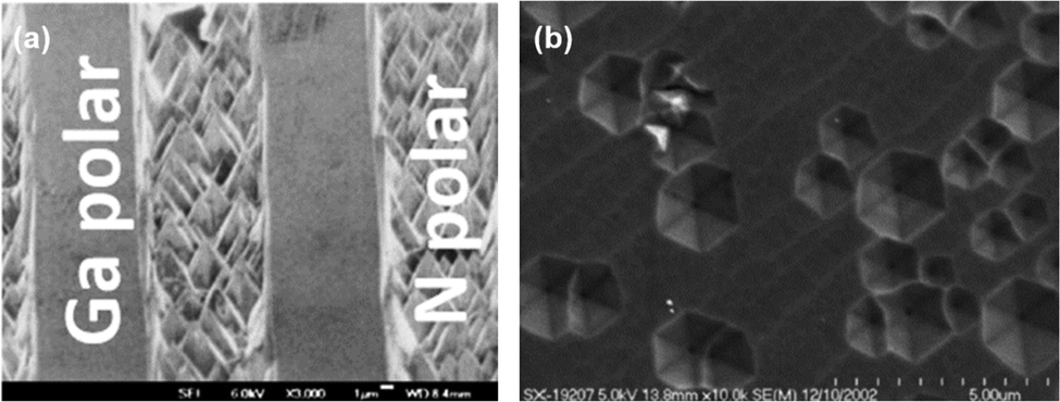 | ||
| Fig. 7 (a) Hexagonal pyramids on the N-polar face of GaN while the surface of the Ga-polar region remained smooth and intact. Reproduced with permission.78 Copyright 2003. AIP Publishing. (b) Dislocation mediated hexagonal etch pits on AlN. Reproduced with permission.82 Copyright 2004. Elsevier. | ||
In the case of α-SiC, the etch rate of the Si face is much slower than the C face under the same etching conditions. In the mixture of 1![[thin space (1/6-em)]](https://www.rsc.org/images/entities/char_2009.gif) :1 KOH and KNO3, the etch rate of the C face was found to be 10 times higher than the Si face, which is attributed to the difference in surface free energy along different faces.84 The shape of the etch pits also depends on the polytypes of the SiC. The etching pits in the case of 3C-SiC was triagonal in nature (Fig. 8(a)).85 On the other hand, the etching pits on 4H- and 6H-SiC were distorted hexagonal with alternating long and short edges in shape (Fig. 8(b)).86
:1 KOH and KNO3, the etch rate of the C face was found to be 10 times higher than the Si face, which is attributed to the difference in surface free energy along different faces.84 The shape of the etch pits also depends on the polytypes of the SiC. The etching pits in the case of 3C-SiC was triagonal in nature (Fig. 8(a)).85 On the other hand, the etching pits on 4H- and 6H-SiC were distorted hexagonal with alternating long and short edges in shape (Fig. 8(b)).86
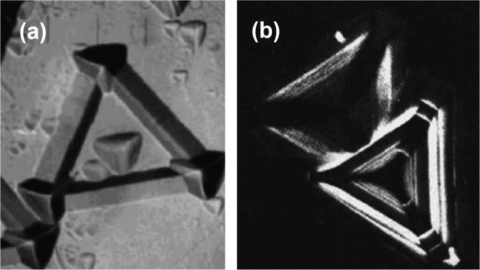 | ||
| Fig. 8 (a) Triangular etch pits in 3C-SiC. Reproduced with permission.85 Copyright 1997, Wiley-VCH. (b) Distorted hexagon etch pits in the 4H and 6H-SiC. Reproduced with permission.86 Copyright 2005, Elsevier. | ||
Treating β-Ga2O3 in hot (130–140 °C) H3PO4 can form etch pits and patterns due to the presence of defects along (![[2 with combining macron]](https://www.rsc.org/images/entities/char_0032_0304.gif) 01) and (101) facets. It was found that three types of defects are associated with these kinds of the etch pits – edge dislocation arrays on (201), plate-like nanopipes on (010) and twin lamellae.87 Similarly, KOH treatment of β-Ga2O3 under an elevated temperature of 140 °C for 2 hours can form triangle and quadrangle shaped etching pits (Fig. 9(a and b)).88 The origin of triangle-shaped etching pits is from dislocation in the [100] depth directions. Quadrangle-shaped etching pits originate from void defects on the (100) crystal surface.
01) and (101) facets. It was found that three types of defects are associated with these kinds of the etch pits – edge dislocation arrays on (201), plate-like nanopipes on (010) and twin lamellae.87 Similarly, KOH treatment of β-Ga2O3 under an elevated temperature of 140 °C for 2 hours can form triangle and quadrangle shaped etching pits (Fig. 9(a and b)).88 The origin of triangle-shaped etching pits is from dislocation in the [100] depth directions. Quadrangle-shaped etching pits originate from void defects on the (100) crystal surface.
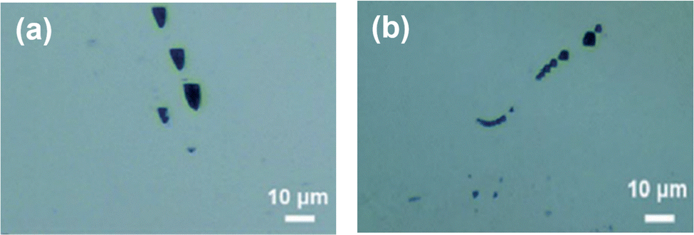 | ||
| Fig. 9 (a) Triangle-shaped and (b) quadrangle-shaped etch pits in the 4H and 6H-SiC. Reproduced with permission.88 Copyright 2020, Royal Society of Chemistry. | ||
Electrochemical etching
Electrochemical etching firstly originated from Bell Labs in 1956 and was applied to nanostructure engineering of Si wafers.89 Subsequently, a surge of research emerged, delving into different electrochemical approaches aimed at etching Si wafers under varied conditions.90,91 Generally, the creation of porous Si structures involves the electrochemical etching of Si wafers in organic solutions, typically acetonitrile (CH3CN) or dimethylformamide (C3H7NO), supplemented with hydrofluoric acid (HF).92 Watanabe and Sakai's 1971 publication marked the initial exploration of the porous characteristics of porous Si. Over the subsequent decades, numerous studies investigating porous Si and its properties were disseminated. The fascination with porous Si nanostructures intensified when Ulrich Gösele detected quantum confinement effects in the absorption spectrum of porous Si. Leigh Canham also observed vibrant red-orange photoluminescence from porous Si nanostructures.93,94 These studies inspired a series of studies aimed at understanding the mechanisms of pore formation and performance regulation to expand applications in the field of optoelectronic devices. Multiple theories regarding the formation mechanisms of porous Si were proposed, encompassing crystallographic face selectivity, enhanced electric field, tunnelling, quantum confinement, and space-charge limitation.95,96In the 1990s, the wet etching of WBG GaN and SiC commenced, and over the years, it has undergone significant development.97 Wet etching proves instrumental in achieving various goals, including revealing defects, addressing polarity issues, enhancing properties, and processing micro/nanostructures such as trenches, holes, grooves, and other targeted patterns. The commonly utilized wet etching technology can be categorized into pure chemical etching methods, encompassing traditional aqueous solution etching and molten salt selective etching, as well as electrochemical etching approaches, mainly including anodic oxidation etching. It is important to note that, due to its extremely low material removal rate and isotropic etching characteristics, pure chemical etching is primarily employed for revealing the defect status of semiconductor surfaces and distinguishing polar planes rather than processing functional micro/nano structures of third-generation semiconductors,98–101 as shown in Fig. 10.
 | ||
| Fig. 10 (a) Electrochemical etching of nanoporous GaN. Reproduced with permission.100 Copyright 2020, American Chemical Society. (b) Electrochemical etching of nanoporous SiC. Reproduced with permission.101 Copyright 2020, IOP Publishing. | ||
Nanowire (NW) structures can also be generated through electrochemical etching, typically evolving from nanoporous structures. It is commonly understood that extended etching time leads to further etching of pore walls, resulting in the formation of NWs. SiC NWs, owing to their improved optoelectronic properties, have significant interest for applications in optoelectronic devices. Zhou et al. pioneered the fabrication of large-scale freestanding n-doped 4H-SiC NW arrays using anodic oxidation etching, demonstrating outstanding performance in the development of piezoelectric nanogenerators.102 Pulsed voltage anodic oxidation etching allows for the production of specialized NW array shapes, such as gourd-shaped NWs, which exhibit remarkable performance in field emission devices.103
Typically, the electrochemical etching process can be delineated into two sequential stages: the initial stage involves oxidizing the semiconductor surface, while the subsequent stage entails dissolving the solid oxidation product with the etching solution, concurrently allowing the escape of gas oxidation products from the semiconductor surface. The redox reaction necessitates both electrons and holes to oxidize the semiconductors.86 The electrochemical etching requires the application of an external bias voltage to furnish the electrons and holes essential for semiconductor oxidation. In these etching processes, the semiconductor slated for etching and the inert counter electrode are connected to the positive and negative terminals of the external voltage, respectively. Consequently, the semiconductor linked to the positive terminal receives an injection of holes, triggering an oxidation reaction. Subsequently, the oxidation products either dissolve in the etching solution or escape. Simultaneously, electrons are consumed at the inert electrode.104,105
Metal assisted chemical etching
Metal assisted chemical etching (MacEtch) was firstly put forward by Li et al. in 2000.106 They found that by immersing the noble metal (Au, Pt, Pd) coated Si wafer in an etchant mixture of oxidant (H2O2) and acid (HF), Si water can be etched vertically. The anisotropic etching characteristic is similar to dry (plasma) etching nonetheless it is a plasma-free process. In Si MacEtch, holes are generated by reduction of H2O2 and H+ catalyzed by the noble metal (cathode reaction). The generated holes then oxidize Si which is dissolved by HF (anode reaction).107 Therefore, due to the continuous oxidizing and dissolving process, Si species underneath the novel metal layer can be removed, forming vertical Si nanostructures.Apart from Si, the application of MacEtch has been extended to other narrow bandgap semiconductors such as Ge and GaAs. Similar as Si, Ge MacEtch typically makes use of an etchant mixture of oxidant (H2O2, KMnO4) and acid (HF).108,109 Nonetheless, as the oxide species of Ge is soluble in water, Ge MacEtch in the absence of acid is also reported.110 Similarly, H2O2 and KMnO4 are widely used as oxidants and HF as the acid in GaAs MacEtch.111,112 However, one distinct difference among MacEtch of Si, Ge and GaAs is the etching characteristic. In most reported Si MacEtch, the forward etching feature was observed, meaning that the Si species underneath the noble metal layer was removed.113 However, in terms of Ge, the inverse-MacEtch (i-MacEtch) is normally seen. In this case, etching happens in the areas not covered by a noble metal layer.114 This is likely from the rapid diffusion of holes away from the metal-coated junction region to the off-area.108 For GaAs MacEtch, both MacEtch and i-MacEtch have been reported, depending on the difference in etching environment.115
MacEtch can been applied to WBG semiconductors such as SiC, Ga2O3 and GaN,116–118 as shown in Fig. 11. Similar as MacEtch of narrow bandgap semiconductors, oxidant (K2S2O8, H2O2, etc.) and acid (HF) are typically necessary in the etchant. Nonetheless, for GaN MacEtch, alkali was used instead of acid. Being different from MacEtch of narrow bandgap semiconductors, UV illumination with the above bandgap photon energy is typically needed for realizing efficient and effective etching of WBG materials during MacEtch. In this case, photons are absorbed by WBG materials, generating holes which participate in oxidizing semiconductor material species, which are further dissolved by etchant. This can be attributed to the WBG characteristic of materials. The valence band of WBG semiconductors could be more negative than the electro potential of oxidant reduction. Therefore, the holes generated from the oxidant reduction reaction may not be injected into semiconductors.107 As a result, an extra source such as UV illumination is necessary to supply holes. This feature of photoinduced etching also leads to the fact that MacEtch of WBG semiconductors exhibits i-MacEtch characteristics. The other distinct feature in MacEtch of WBG semiconductors is that the material which can be etched is limited to n-type doping. This could be attributed to the surface band structures. As in the case of p-type semiconductors, the surface upward bending could drive the photogenerated holes away from the semiconductor/etchant interface. Therefore, the etching efficiency is greatly limited.
 | ||
| Fig. 11 (a) SiC nanopillar structures formed by MacEtch. Reproduced with permission.116 Copyright 2021, Wiley-VCH. (b) Ga2O3 fin structures formed by MacEtch. Reproduced with permission.117 Copyright 2019, American Chemical Society. (c) GaN nanopillar structures formed by MacEtch. Reproduced with permission.118 Copyright 2021, American Vacuum Society. | ||
Applications in photodetection
Table 2 summarizes selected studies in which micro/nanostructured photodetectors were fabricated using different top-down etching techniques. The values of dark current and response speed often depend on factors such as material quality, surface states introduced during etching, and any subsequent passivation. In contrast, responsivity commonly increases due to enhanced light-trapping and reduced UV reflectance on the textured surface. Detailed explanations are provided in the respective sections.| Material | Etching technique | Ref. | Nanostructure description | Responsivity | Dark current | Response speed |
|---|---|---|---|---|---|---|
| GaN | Plasma | 119 | Nanowire | — | 0.005 nA at 5 V bias | — |
| GaN | Plasma | 120 | Nanohole array | Increased from 55.7 × 10² to 1.4 × 10⁵ A W−1 at 325 nm, 5 V bias | Decreased from 98.1 to 15 nA at 5 V bias | τ rise increased from 36 to 64 ms under 325 nm at an on/off pulse interval of 10 s |
| SiC | Plasma | 121 | Nanocone array | 0.078 A W−1 at 320 nm, −0.5 V bias | 1 × 10⁻³ nA at −0.5 V bias | τ rise: 1.7 ms under 360 nm with −0.5 V bias |
| SiC | Plasma | 122 | Microhole array | Increased from 0.01 to 0.063 A W−1 at 270 nm, 5 V bias | 5 × 10⁻⁶ nA at 5 V bias | τ rise: 1.9 × 10⁻⁶ ms under 266 nm with 10 V bias |
| Ga2O3 | Plasma | 123 | Nanowire | Increased from 0.01 to 0.122 A W−1 at 260 nm, 5 V bias | Decreased | τ rise decreased from 152 to 34 ms under 266 nm with 5 V bias |
| Ga2O3 | Plasma | 45 | Thinned flake | — | 100 μA at 5 V bias | τ rise: 1.4 s under 254 nm |
| Diamond | Plasma | 124 | Nanowire | 388 A W−1 at 350 nm, 0 V bias | 70 nA at 300 nm | τ rise: 24 ms under 300 nm with 0 V bias |
| SiC | Electrochemical | 125 | Pores | 0.20 A W−1 at 340 nm, 5 V bias | — | — |
| (Al)GaN | Electrochemical | 126 | Pores | Increased from 1.3 to 19.4 A W−1 at 254 nm, 5 V bias | Decreased | τ rise decreased from 10 ms to 6 μs under 254 nm with 5 V bias |
| Ga2O3 | MacEtch | 127 | Groove textured | Increased from 1.3 to 71.7 A W−1 at 254 nm, −6 V bias | Increased from 0.015 to 1.58 nA at −6 V bias | — |
| GaN | MacEtch | 128 | Nanoridge | Increased from 18 to 115 A W−1 at 365 nm, 3 V bias | Decreased | τ rise increased from 0.8 to 2.1 s under 365 nm with 3 V bias |
Plasma etched GaN nanostructure
A plasma etching process was employed to fabricate p–i–n NW GaN PDs.119 The fabrication process flow is illustrated in Fig. 12(a). The P–i–n GaN structure was epitaxially grown on sapphire by using metal–organic vapor phase epitaxy. An SiO2 layer was deposited on the epitaxial layer. Next, 1 μm polystyrene nanospheres were dispersed on the p–i–n wafers for the masking purpose. After that, polystyrene nanospheres were treated with oxygen plasma to shrink down the size of the polystyrene nanospheres. A CHF3 chemistry-based plasma process was carried out to etch the SiO2 layer uncovered by polystyrene nanospheres. Subsequently, BCl3–Cl2 chemistry in ICP-RIE was used for deep etching of GaN to form the NWs. The schematic of the fabricated PD is featured in Fig. 12(b). The response of NW PD can be observed from the I–V characteristics in Fig. 12(c) where an increase in photocurrent is evident.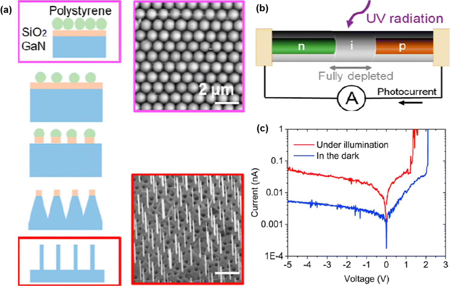 | ||
| Fig. 12 (a) Fabrication process steps and FESEM image of GaN NW. (b) Schematic of p–i–n GaN NW PD. (c) I–V characteristics of GaN NW PD. Reproduced with permission.119 Copyright 2023, American Chemical Society. | ||
Periodic nanoholes were fabricated on the AlGaN/GaN high electron mobility transistor (HEMT) structure to improve photon absorption of metal–semiconductor–metal (MSM) PD.120 Electron beam lithography (EBL) was firstly used to pattern the nano-hole array. Next, ICP-RIE plasma etching was carried out with a BCl3/Cl2 gas mixture to etch the AlGaN layer. As shown in Fig. 13(a), the diameter and depth of etching hole were 150 nm and 42.3 nm respectively. The simulation results predicted that the reflectance was reduced and electric field was concentrated with increased etching hole size (Fig. 13(b and c)). The nanohole array enhanced light trapping to prolong their path into the GaN layer, which attributed to increased photocarrier generation (Fig. 13(d)). As a result, around four orders magnitude of increment in photocurrent was noticed (Fig. 13(e)). The responsivity, photo to dark current ratio and detectivity of the nanohole PDs were found to be 1 × 10⁵ (A W−1) (Fig. 13(f)), 103 and 4.9 × 10¹⁴ Jones, respectively. It is worth mentioning that the PD with a flat surface had 106 times lower detectivity as compared to the PD with nanohole arrays. These findings illustrate how plasma-etched GaN nanostructures reduce reflectivity and increase light absorption, thereby boosting photocurrent and responsivity for UV photodetection.
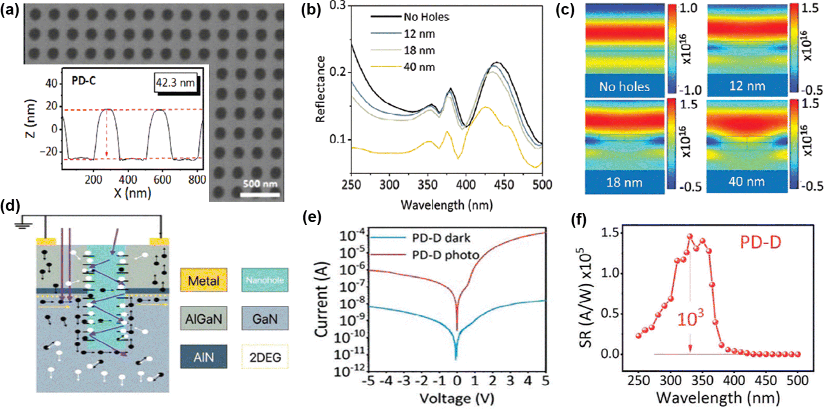 | ||
| Fig. 13 (a) FESEM and AFM image of nanohole array AlGaN/GaN. Simulated (b) reflectance and (c) electric field profile with and without nanoholes. (c) Schematic of AlGaN/GaN PD. (d) Photodetection mechanism. (e) I–V characteristics and (f) spectral response of the AlGaN/GaN nanohole array PD. Reproduced with permission.120 Copyright 2024, Wiley-VCH. | ||
Plasma etched SiC nano/microstructure
PD made of 4H-SiC p–i–n vertical nano-cone (NC) array structure was demonstrated by Guo et al. (Fig. 14).121 They firstly grew a 4H-SiC p–i–n structure on an n-type SiC substrate by high-temperature chemical vapor deposition (HTCVD). The fabrication steps are displayed in (Fig. 14(a)). Ni was deposited as a etch mask in accordance with EBL. After that, ICP-RIE was carried out to etch SiC uncovered by the Ni etch mask. After etching, the Ni etch mask was removed by HCl. The SEM image of the SiC NW array is shown in Fig. 14(b). Indium tin oxide (ITO) was deposited as electrodes for electrical connection in the p-side. On the other hand, Ni was used for n-contact. A schematic of the fabricated device is shown in Fig. 14(c). The top diameter, bottom diameter, and height of the single nanocolumn were 200 nm, 480 nm, and 1800 nm, respectively. Peak responsivity of the PD reached about 78 mA W−1 at 320 nm. Moreover, due to surface passivation of SiC against the surface defects of SiC NC, a fast response (rise time = 1.7 ms and fall time = 1.8 ms) was achieved (Fig. 14(d)).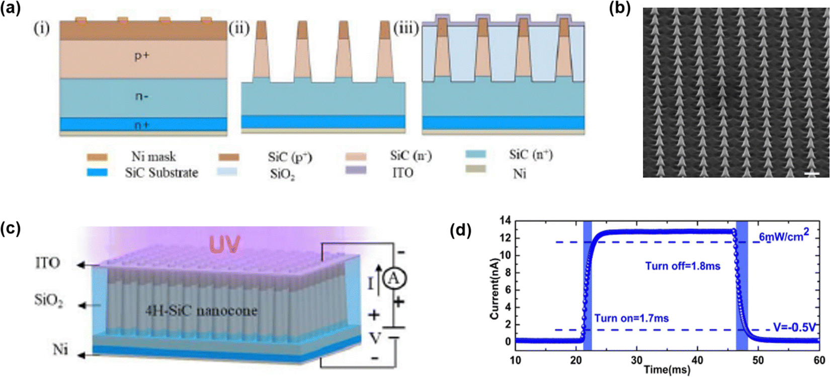 | ||
| Fig. 14 Schematic of (a) the fabrication process steps and (b) FESEM image of the 4H-SiC NC array with a scale bar of 1 μm. (c) Diagram of p–i–n 4H-SiC NC PD. (d) Transient characteristics of the 4H-SiC NC array PD. Reproduced with permission.121 Copyright 2021, IEEE Publishing. | ||
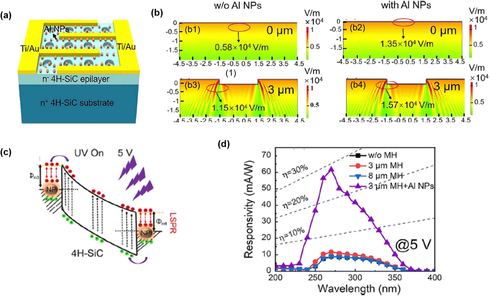
An enhanced photodetection performance was observed by localized surface plasmon resonance (LSPR) of Al nanoparticles (NPs) inside the etching micro-hole (MH) arrays of 4H-SiC MSM PDs (Fig. 15(a)).122 The fabrication of MH on SiC was accomplished by photolithography, followed by ICP-RIE. Etching was performed at 10 °C with a 30 sccm (CF4)/5 sccm (O2) gas flow rate. The average hole depth was 400 nm. The Al NPs were embedded into the MH region to enable LSPR. In order to embed Al NPs, 5 nm Al thin film was deposited and annealed at 500 °C under ambient N2. Fig. 15(b1–b4) exhibit the simulated electric field distribution, which reveals that SiC MH with Al NPs created the maximum electric field. The concentrated electric field distribution resulted in better light trapping. The Al NPs in contact with SiC formed the localized depletion regions where the electric field rapidly swept away the photogenerated carriers (Fig. 15(c)). The 600% increment in responsivity was achieved in the case of the Al NP embedded MH array PD as compared to conventional flat 4H-SiC MSM PD ((Fig. 15(d)). Hence, plasma-etched SiC micro- and nanostructures lead to enhanced responsivity and faster response times, underscoring the direct correlation between etching-induced surface texturing and improved UV detection capabilities.
 | ||
| Fig. 15 (a) Schematic of 4H-SiC MSM PD with Al nanoparticles embedded in the micro-hole. Electric field distribution of the device (b-1) without Al nanoparticles, (b-2) with Al nanoparticles, (b-3) with micro hole and (b-4) with a micro hole and Al nanoparticles. (c) Charge transfer process between 4HSiC and Al NPs at 5 V. (d) Spectral response of PD. Reproduced with permission.122 Copyright 2023, American Chemical Society. | ||
Plasma etched Ga2O3 nano/microstructure
Vertical β-Ga2O3 NW arrays were fabricated to improve the photodetection capability by enhancing the light trapping as compared to the flat film of β-Ga2O3.55,123 The fabrication process steps are described in Fig. 16(a). The fabrication process started with the deposition of a 10 nm Ni layer. Next, the sample was annealed under ambient N2 at 850 °C for 3 min to form Ni NPs which work as the etching mask. BCl3/Ar gas chemistry based ICP-RIE treatment was carried out to form the NW array. The SEM image of the cross-sectional view of the NW array is displayed in Fig. 16(b). MSM electrodes of Ti/Au (20/80 nm) were deposited to complete the PD fabrication process. Presence of stronger light field intensity in the case of the NW array signifies better light trapping is responsible for higher photocurrent in β-Ga2O3 PD with the NW array as compared to the flat surface (Fig. 16(c)). The I–V characteristics of Ga2O3 PD with and without NW are presented in Fig. 16(d). Lower dark current in NW Ga2O3 PD was expected due to lower defects and oxygen vacancies. Higher photocurrent in Ga2O3 NW PD was achieved due to better light trapping. The Ga2O3 NW PD had a responsivity of 0.122 A W−1, which was 10 times higher than that of flat surface Ga2O3 PD.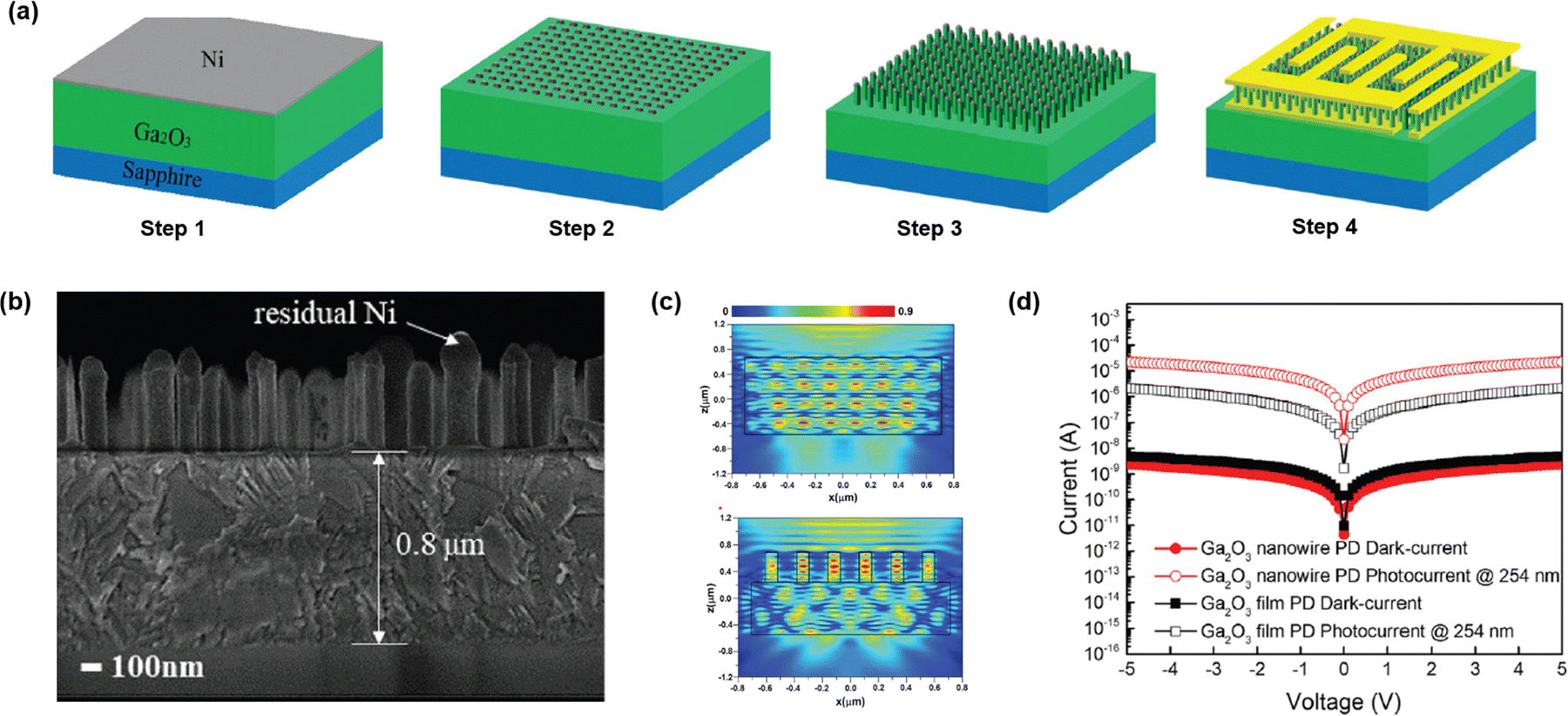 | ||
| Fig. 16 (a) Schematic of the fabrication process steps of β-Ga2O3 NW PD. (b) FESEM image of the β-Ga2O3 NW array. Comparison of (c) light field intensity of NW and flat surface β-Ga2O3. (d) I–V characteristics of PD with and without a NW array. Reproduced with permission.123 Copyright 2020, De Gruyter. | ||
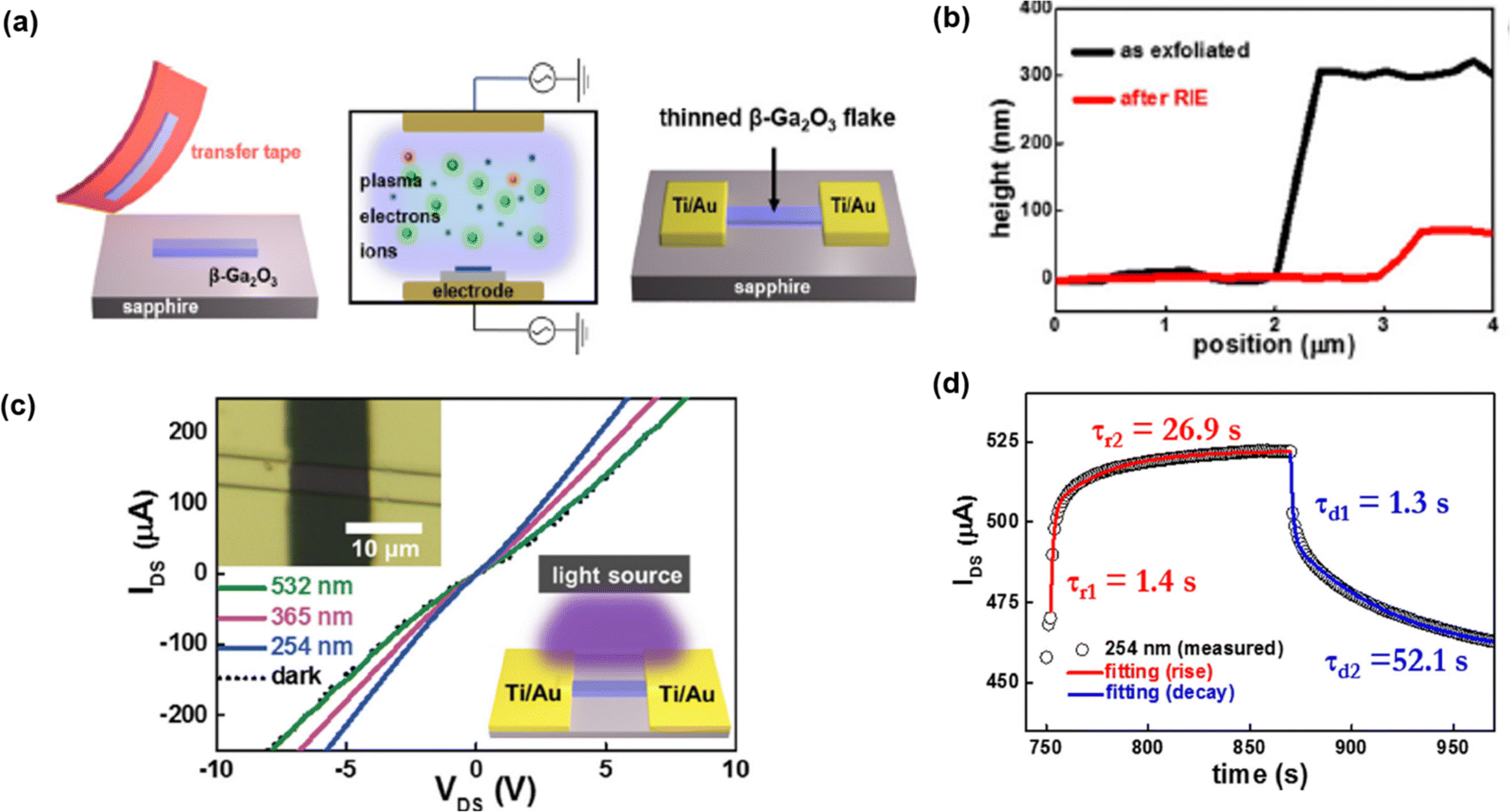
An RIE based technique was employed to convert three dimensional β-Ga2O3 into ultrathin micro-flakes. β-Ga2O3 micro-flakes were used to make UV PD.45 The fabrication process is depicted in Fig. 17(a). In order to realize β-Ga2O3 micro-flakes, β-Ga2O3 flakes were prepared by a conventional mechanical exfoliation method. SF6 gas-based RIE plasma etching was processed to thin down β-Ga2O3 with a thickness below 100 nm as confirmed by AFM characterization (Fig. 17(b)). Ti/Au electrodes were deposited for electrical connection. The I–V characteristic (Fig. 17(c)) shows that the photoresponse of the fabricated PD, leading to the noticeable response under the illumination of 254 nm and 365 nm wavelengths. As the bandgap of β-Ga2O3 is 4.9 eV, it should not respond to the wavelength of 365 nm. However, it indicates a photoresponse even under 365 nm illumination due to the presence of intrinsic defects including oxygen vacancies. The rise and fall time were recorded as 1.4 and 1.3 seconds, respectively for the 254 nm wavelength (Fig. 17(d)), which are comparable to the un-etched β-Ga2O3. The creation of Ga2O3 nanowire arrays via plasma etching demonstrates that lowering dark current and promoting stronger light absorption can significantly improve photodetector performance in the UV region.
 | ||
| Fig. 17 (a) Schematic of the fabrication process steps of β-Ga2O3 micro-flakes PD. (b) AFM image showing thinning of the flakes. (c) I–V characteristics and (d) transient response of PD. Reproduced with permission.45 Copyright 2017, AIP Publishing. | ||
Plasma etched diamond nano/microstructures
A new design of PD based on vertically aligned ultra-nanocrystalline diamond (UNCD) NW was demonstrated. It consisted of 110 UNCD NW situated between two pair of electrodes, one external pair and one internal pair (Fig. 18(a)).124 UNCD was deposited on tungsten coated Si substrate. The detailed fabrication process is discussed elsewhere.129 Hydrogen silsesquioxane was spin coated on the UNCD surface as a resist. EBL was employed for nanopatterning. After pattering, two step ICP-RIE was carried out. First oxygen-based RIE formed UNCD NWs and then tungsten/Si undercutting were realized by fluoride-based RIE. The SEM image of UNCD NW is shown in Fig. 18(b). Ti/Au metal alloy was deposited for electrode formation. The device could operate under self-biasing mode. Peak responsivity and UV-Vis rejection ratio were measured to be 388 A W−1 and 1 × 10⁵, respectively (Fig. 18(c)). The response time was as fast as 20 ms. These UNCD NW arrays, fabricated through ICP-RIE, exhibit higher responsivity and faster response, validating the effectiveness of plasma etching in forming vertically aligned nanostructures that enhance photo-to-carrier conversion.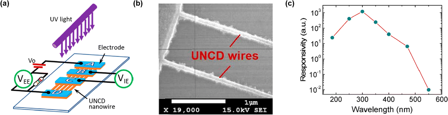 | ||
| Fig. 18 (a) Schematic of NW UNCD PD. (b) FESEM image showing NW UNCD. (c) Spectral response of fabricated PD. Reproduced with permission.124 Copyright 2019, American Chemical Society. | ||
Electrochemical etched SiC nanostructure PD
Nanoporous SiC often exhibits optical or electrical properties that surpass those of pristine bulk SiC. Many researchers have delved into exploring the correlation between the luminescence properties and the porous structure of nanoporous SiC formed through electrochemical etching.130–132 It was discovered that the photoluminescence (PL) performance of SiC, following anodic oxidation etching, was significantly influenced by its morphology. Porous SiC demonstrated a marked enhancement in PL intensity compared to bulk SiC. Similarly, in the research conducted by Dao et al.,97 nanoporous SiC was achieved through electrochemical etching, and varying characteristics of porous SiC were obtained by employing different HF concentrations and etching durations. The PL of porous SiC with distinct features was compared. Parallel to the findings of Drop et al., all forms of porous SiC exhibited heightened PL intensity, which increased with longer etching time. The augmentation of PL intensity primarily stems from the enhanced internal light scattering and the alleviation of internal stress facilitated by the porous structure. Naderi et al. prepared a visible blind UV PD based on porous 6H-SiC through electrochemical etching.125 As shown in Fig. 19(a–c), for different current densities of 10, 15 and 20 mA cm−2, the respective percentages of porosity were observed to be 52, 68, and 72%, which signified that porosity increased with the applied current density. The porosity of SiC also influenced the PD characteristics. From Fig. 19(d), it is clear that the responsivity and quantum efficiency of the PDs increased as the porosity increased which attributes to elevation in the light absorption. Thus, electrochemical etching of SiC to form nanoporous structures effectively increases internal light scattering and reduces surface reflection, resulting in higher responsivity and improved device performance. | ||
| Fig. 19 Surface morphology of nanoporous SiC structure under different etching current densities: (a) 10, (b) 15, and (c) 20 mA cm−2. (d) Spectral responsivity of PDs based on different nanoporous SiC structures. Reproduced with permission.125 Copyright 2013, Elsevier. | ||
Electrochemical etched (Al)GaN nanostructure PDs
GaN with micro and nanostructures exhibit outstanding photoelectrochemical properties, prompting considerable research efforts to fabricate such structures through electrochemical etching methods. Vajpeyi et al. successfully generated porous GaN with an average pore size of approximately 85–90 nm using photoelectrochemical etching with HF solution as the electrolyte.133 Their investigation of the optical properties revealed a significant enhancement in the PL intensity of porous GaN compared to the pristine counterpart. The observed red shift of the E-2 (high) phonon peak in the Raman spectrum was attributed to compressive stress relaxation in porous GaN and the improved crystal quality resulting from photoelectrochemical etching. In the study conducted by Al-Heuseenet et al.,134–136 detailed examinations were carried out on current density and various electrolytes (H2SO4 & H2O2, KOH, HF & HNO3, HF & C2H5OH) in the process of generating porous GaN. The results indicated a substantial enhancement in the PL spectral peak intensity of porous GaN, along with improved stress state, compared to the pristine sample. From the aforementioned reports, it is evident that the porous morphology is highly dependent on the type of electrolyte and current density. Zhao et al. developed an AlGaN-based deep ultraviolet distributed Bragg reflector (DBR) based on electrochemical lateral etching,137 which has a reflectivity of 95% at 280 nm. It became the basis of AlGaN-based microcavity structures for deep UV (DUV) PDs.Zheng et al. prepared nanoporous AlGaN through electrochemical etching and fabricated UV PDs, which produced better performance as compared to planar AlGaN PD.126 During the electrochemical process, they used 1% KOH as the electrolyte and platinum (Pt) plate as the anode and cathode with the potential difference of 40 V. For comparison, one half of an AlGaN on sapphire wafer was treated with an electrochemical etching procedure for 5 minutes to make nanoporous PDs, and another half was untreated to make planar PDs (Fig. 20(a)). As depicted in Fig. 20(b), the surface reflectivity of the NP AlGaN PD was suppressed from 18 to 1% while comparing with the planar surface. In Fig. 20(c), the larger electric field intensity distributions in nanoporous AlGaN as compared to planar AlGaN clearly indicates that the nanoporous structure facilitates enhanced photon capture capabilities. Nanoporous structures, which have fewer carrier transport channels due to etching porosity and increased resistance, can reduce the dark current. Meanwhile, owing to the enhanced photon absorption, these nanoporous structures produced a higher photocurrent as compared to that of planar PDs (Fig. 20(e)). With lower dark current and higher photocurrent, the detectivity of the nanoporous AlGaN PD not only reached 1.5 × 10¹³ Jones but also showed ultra-fast response (6–7 ms) due to effective defect passivation. By introducing nanoporous AlGaN through electrochemical etching, the resultant reduction in surface reflectivity and dark current directly translates into superior detectivity and faster photoresponse, highlighting the clear relationship between nanostructuring and UV PD performance.
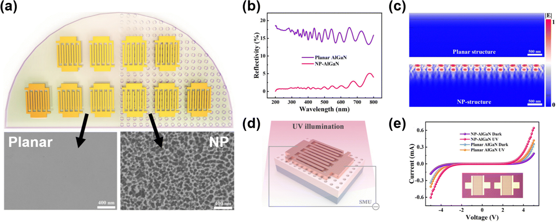 | ||
| Fig. 20 (a) AlGaN electrochemical etching process and MSM PD fabrication; (b) spectral reflectivity of AlGaN before and after electrochemical etching; (c) simulated electric field distribution comparison between planner and nanoporous AlGaN; (d) schematic of AlGaN nanoporous PD; (e) I–V characteristic curve of nanoporous and planar PD under dark and UV exposure. Reproduced with permission.126 Copyright 2023, Royal Society of Chemistry. | ||
MacEtched Ga2O3 nanostructure PD
Due to the anisotropic etching characteristic, the effective antireflective nanostructures are mostly fabricated via dry etching. However, surface damage from plasma could lead to degraded device performance.138 Therefore, as the alternative of dry etching in realizing anisotropic etching features, MacEtch has been employed in Ga2O3 in fabricating antireflective nanostructures for PD applications. In Kim et al.'s work,127 MacEtch was employed on (010) β-Ga2O3 substrates in an etchant mixture of K2S2O8 and HF under 254 nm UV illumination. The nanogroove structures with depth and height of 120 and 150 nm, respectively, were fabricated (Fig. 21(a)). Such surface texturing was able to realize a 20% reduction in UV reflection, therefore enhanced UV absorption was achieved (Fig. 21(b)). The fabricated MSM PD based on textured β-Ga2O3 substrate showed a responsivity of 71.7 A W−1 compared with 1.3 A W−1 on planar β-Ga2O3 substrate (Fig. 21(c)). However, despite the enhanced responsivity, MacEtch led to the oxygen deficiency in β-Ga2O3. Such a surface condition resulted in reduced Schottky barrier height and higher dark current in PD (Fig. 21(d)). Therefore, further optimization of the MacEtch process should be explored to enhance PD performance. Although MacEtched Ga2O3 offers enhanced responsivity by virtue of improved light absorption via nanogrooves, balancing surface defect generation and dark current remains a critical optimization step. | ||
| Fig. 21 (a) SEM image of β-Ga2O3 nanogroove surface texturing. (b) Surface reflection spectra of β-Ga2O3 before and after MacEtch texturing. (c) Responsivity and (d) dark current of MSM PDs based on planar and textured β-Ga2O3. Reproduced with permission.127 Copyright 2018, AIP Publishing. | ||
MacEtched GaN nanostructured PDs
Similar as β-Ga2O3, MacEtch can also be employed in GaN for PD applications. In Guo et al.'s work,139 porous GaN was fabricated on undoped, lightly n-doped, and heavily n-doped GaN wafers (Fig. 22(a) and (b)) via Pt-assisted MacEtch in an etchant mixture of H2O2 and HF under UV illumination. By fabricating UV PDs, they found that such porous structures could distinctly boost the photoresponse of UV PDs based on doped GaN wafer (Fig. 22(c)). However, degradation of the PD performance on undoped GaN wafer was observed (Fig. 22(c)), which was attributed to the increased defect density after MacEtch. In comparison, Liao et al. fabricated nanoridge texturing on undoped GaN via MacEtch. The PD exhibited an 8 times responsivity enhancement compared with that of the planar GaN PD128 (Fig. 22(d) and (e)). Such discrepancy can be from the difference in etching recipe and environment as they directly determine the surface condition and morphology of etched GaN which affect the PD performance significantly. Although the plasma-induced surface damage could be avoided in MacEtch, unfavorable surface conditions such as porous and amorphous layers with an increase in defect density is unavoidable.108,140 Therefore, appropriate post-etching treatment has been reported to repair the surface damage from MacEtch for potential device level applications.116,140 Collectively, these studies reveal how MacEtch can achieve substantial responsivity gains in GaN-based UV PDs by reducing surface reflection, yet appropriate post-etching treatments may be necessary to mitigate defect-induced dark current.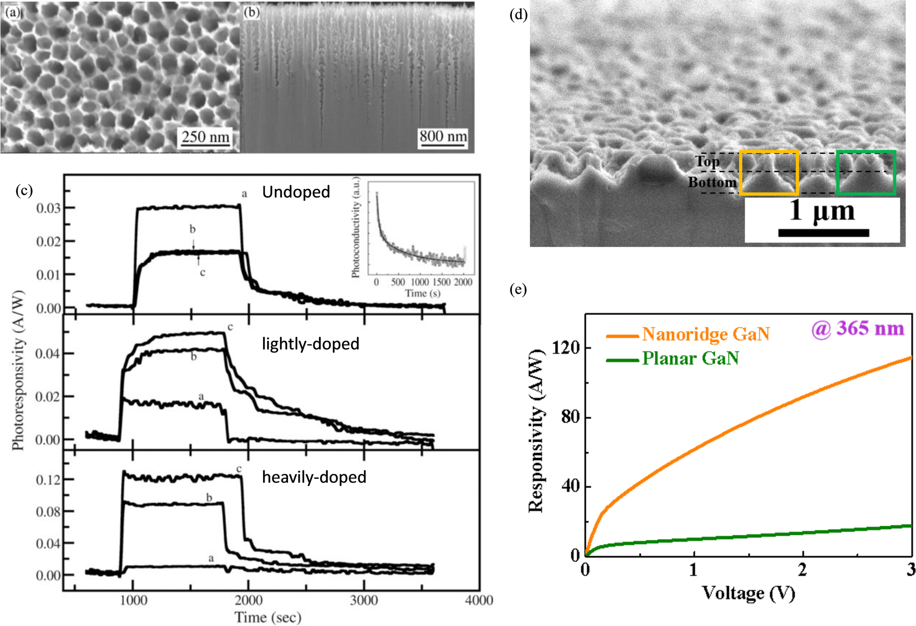 | ||
| Fig. 22 (a) Top and (b) cross-sectional SEM images of GaN porous structures. (c) Photoresponse of MSM PDs based on GaN samples with different doping concentrations indicated in subfigures. Curves labeled as (a), (b) and (c) correspond to unetched, 1-hour etched, and 2-hour etched GaN samples, respectively. Reproduced with permission.139 Copyright 2006, Elsevier. (d) Cross-sectional SEM images of GaN nanoridge structures. (e) UV photoresponse of MSM PDs based on planar and nanoridge textured GaN surfaces. Reproduced with permission.128 Copyright 2023, American Chemical Society. | ||
Outlook and conclusions
In summary, we have reviewed top down dry and wet etching techniques for III-nitride, SiC, Ga2O3, and diamond. We have also presented a comprehensive summary on the applications of those etching techniques to make micro and nanostructured UV PDs. Enhanced light trapping results in performance improvement of PDs.Though plasma etching is the main process for fabricating nano and microstructures, it induces damages to the etched surface. The plasma defects can be mitigated by post-chemical or thermal treatment. Micro/nano-structuring of III-nitride, SiC, Ga2O3, and diamond via plasma etching has been adapted widely to improve the photoresponse of PDs. Apart from plasma etching, LST with the assistance of a femto-second laser is also employed to make microstructures of WBG semiconductors. However, micro-structuring by means of LST has not been adopted to date for performance improvement of third generation or WBG-based PDs, which defines an achievable research gap to be explored.
Though plasma etching is the most widely used technique to achieve micro/nano-structuring, wet etching routes are also being adapted. Controlling anisotropy is a challenge in the case of wet etching. However, some advanced wet etching techniques such as MacEtch, electrochemical etching, and crystal plane and defect dependent wet etching have exhibited controllable anisotropy etching behavior. MacEtch has been adapted to fabricate nano/micro-structuring for GaN and Ga2O3-based UV PDs, which contribute to performance improvement. In addition, MacEtch has been adapted to make antireflective surface structuring in SiC. Further research can be extended to the demonstration of nano/micro-structuring of SiC, resulting in superior PD performance. MacEtch of diamond has not been achieved yet. MacEtch of WBG semiconductors needs above bandgap UV illumination which excites photoelectrons and holes. Due to an ultra-wideband gap of 6.5 eV, it is difficult to excite diamond and fail to achieve MacEtch of diamond, which could be a future research direction.
It is evident that crystal plane and defect dependent wet etching result in ordered micro/nano-structuring of III-nitride, SiC, and Ga2O3. Being a very inert material, it is very difficult to impose crystal plane dependent wet chemical etching in diamond. Though this kind of wet etching is mostly utilized to reveal the defects in the crystals, this technique can be adapted to induce light trapping in diamond for the advanced DUV PDs.
Currently, electrochemical etching stands out as the most widely adopted wet etching approach for third-generation semiconductors. In comparison to pure chemical etching, electrochemical etching offers a more diverse range of processing targets and structures. It enables us to develop various anisotropic etching outcomes. However, few examples of electrochemical etching on III-nitride and SiC for UV PDs have been reported, which makes room for further research in this area. More specifically, electrochemical etching has not been employed to fabricate Ga2O3 and diamond-based UV PDs to date. Therefore, continued advances in both conventional and unconventional etching techniques such as LST, MacEtch, electrochemical etching, and crystal plane sensitive etching can provide an avenue for the development of future advanced high-performance UV PDs.
Data availability
All data required to evaluate the conclusions of the dissertation appear in the paper and/or the ESI.† Other relevant data supporting the findings of this study are available from the corresponding author upon reasonable request. Source data are provided with this paper.Conflicts of interest
There are no conflicts to declare.Acknowledgements
This work was supported by the A*STAR, Singapore, Advanced Manufacturing and Engineering (AME) Individual Research Grant (IRG) under the Project M21K2c0107 and M23M6c0099.References
- W. Zhao, The Application Status of the Third Generation of Semiconductor Materials in the FIeld of Electric Power, Highlight Sci. Eng. Technol., 2023, 53, 194–198 CrossRef.
- P. Neininger, M. Mikulla, P. Döring, M. Dammann, F. Thome, S. Krause, D. Schwantuschke, P. Brückner, C. Friesicke and R. Quay, Advances in GaN Devices and Circuits at Higher Mm-Wave Frequencies, E-Prime - Adv. Electr. Eng. Electron. Energy, 2023, 4, 100177, DOI:10.1016/j.prime.2023.100177.
- N. Islam, M. F. P. Mohamed, M. F. A. J. Khan, S. Falina, H. Kawarada and M. Syamsul, Reliability, Applications and Challenges of GaN HEMT Technology for Modern Power Devices: A Review, Crystals, 2022, 12(11), 1581, DOI:10.3390/cryst12111581.
- A. Udabe, I. Baraia-Etxaburu and D. G. Diez, Gallium Nitride Power Devices: A State of the Art Review, IEEE Access, 2023, 11, 48628–48650, DOI:10.1109/ACCESS.2023.3277200.
- J. He, W. Cheng, Q. Wang, K. Cheng, H. Yu and Y. Chai, Recent Advances in GaN-Based Power HEMT Devices, Adv. Electron. Mater., 2021, 7(4), 2001045, DOI:10.1002/aelm.202001045.
- R. K. Mondal, S. Adhikari, V. Chatterjee and S. Pal, Recent Advances and Challenges in AlGaN-Based Ultra-Violet Light Emitting Diode Technologies, Mater. Res. Bull., 2021, 140, 111258, DOI:10.1016/j.materresbull.2021.111258.
- R. K. Mondal, V. Chatterjee and S. Pal, Hole Transport in Ultraviolet Light-Emitting Diode via p-Type Injection Channel, IEEE Trans. Electron Devices, 2021, 68(5), 2320–2325, DOI:10.1109/TED.2021.3064784.
- M. Kneissl, T.-Y. Seong, J. Han and H. Amano, The Emergence and Prospects of Deep-Ultraviolet Light-Emitting Diode Technologies, Nat. Photonics, 2019, 13(4), 233–244, DOI:10.1038/s41566-019-0359-9.
- Y.-Y. Zhang, Y.-X. Zheng, J.-Y. Lai, J.-H. Seo, K. H. Lee, C. S. Tan, S. An, S.-H. Shin, B. Son and M. Kim, High Performance Flexible Visible-Blind Ultraviolet Photodetectors with Two-Dimensional Electron Gas Based on Unconventional Release Strategy, ACS Nano, 2021, 15(5), 8386–8396, DOI:10.1021/acsnano.0c10374.
- R. K. Mondal, Z. Xiong, M. K. Ghimire, R. Lingaparthi, D. Nethaji, K. Radhakrishnan and M. Kim, Enhanced Performance of Ultraviolet AlGaN/GaN Photo-HEMTs by Optimized Channel Isolation Schemes, Adv. Opt. Mater., 2024, 12(12), 2302602, DOI:10.1002/adom.202302602.
- Q. Cai, H. You, H. Guo, J. Wang, B. Liu, Z. Xie, D. Chen, H. Lu, Y. Zheng and R. Zhang, Progress on AlGaN-Based Solar-Blind Ultraviolet Photodetectors and Focal Plane Arrays, Light: Sci. Appl., 2021, 10(1), 94, DOI:10.1038/s41377-021-00527-4.
- H. K. Raut, V. A. Ganesh, A. S. Nair and S. Ramakrishna, Anti-Reflective Coatings: A Critical, in-Depth Review, Energy Environ. Sci., 2011, 4(10), 3779, 10.1039/c1ee01297e.
- H. Zhao, Y. Lee, M. Han, B. K. Sharma, X. Chen, J.-H. Ahn and J. A. Rogers, Nanofabrication Approaches for Functional Three-Dimensional Architectures, Nano Today, 2020, 30, 100825, DOI:10.1016/j.nantod.2019.100825.
- S. J. Pearton, E. A. Douglas, R. J. Shul and F. Ren, J. Vac. Sci. Technol., A, 2020, 38, DOI:10.1116/1.5131343.
- G. Mak, E. Lam and H. Choi, J. Vac. Sci. Technol., B, 2010, 28, 380–385, DOI:10.1116/1.3359593.
- Y.-Y. Lai, S.-C. Hsu, H.-S. Chang, Y. S. Wu, C.-H. Chen, L.-Y. Chen and Y.-J. Cheng, Res. Chem. Intermed., 2017, 43, 3563–3572, DOI:10.1007/s11164-016-2430-1.
- R. P. Srivastava and D. Y. Khang, Adv. Mater., 2021, 33, 2005932, DOI:10.1002/adma.202005932.
- F. Yam, Z. Hassan and S. Ng, Thin Solid Films, 2007, 515, 3469–3474, DOI:10.1016/j.tsf.2006.10.104.
- H. P. Gillis, D. A. Choutov and K. P. Martin, The Dry Etching of Group III-Nitride Wide-Bandgap Semiconductors, JOM, 1996, 48(8), 50–55, DOI:10.1007/BF03223028.
- C. H. Chiu, P. Yu, H. C. Kuo, C. C. Chen, T. C. Lu, S. C. Wang, S. H. Hsu, Y. J. Cheng and Y. C. Chang, Broadband and Omnidirectional Antireflection Employing Disordered GaN Nanopillars, Opt. Express, 2008, 16(12), 8748, DOI:10.1364/OE.16.008748.
- H.-K. Sung, T. Qiang, Z. Yao, Y. Li, Q. Wu, H.-K. Lee, B.-D. Park, W.-S. Lim, K.-H. Park and C. Wang, Vertical and Bevel-Structured SiC Etching Techniques Incorporating Different Gas Mixture Plasmas for Various Microelectronic Applications, Sci. Rep., 2017, 7(1), 3915, DOI:10.1038/s41598-017-04389-y.
- S. J. Pearton, J. Yang, P. H. Cary, F. Ren, J. Kim, M. J. Tadjer and M. A. Mastro, A Review of Ga2O3 Materials, Processing, and Devices, Appl. Phys. Rev., 2018, 5(1), 011301, DOI:10.1063/1.5006941.
- J. Enlund, J. Isberg, M. Karlsson, F. Nikolajeff, J. Olsson and D. J. Twitchen, Anisotropic Dry Etching of Boron Doped Single Crystal CVD Diamond, Carbon, 2005, 43(9), 1839–1842, DOI:10.1016/j.carbon.2005.02.022.
- Properties, Processing and Applications of Gallium Nitride and Related Semiconductors .
- S. J. Pearton, R. J. Shul and F. Ren, A Review of Dry Etching of GaN and Related Materials, MRS Internet J. Nitride Semicond. Res., 2000, 5(1), e11, DOI:10.1557/S1092578300000119.
- J. Lee, H. Cho, D. C. Hays, C. R. Abernathy, S. J. Pearton, R. J. Shul, G. A. Vawter and J. Han, Dry Etching of GaN and Related Materials: Comparison of Techniques, IEEE J. Sel. Top. Quantum Electron., 1998, 4(3), 557–563, DOI:10.1109/2944.704117.
- K. H. Baik and S. J. Pearton, Dry Etching Characteristics of GaN for Blue/Green Light-Emitting Diode Fabrication, Appl. Surf. Sci., 2009, 255(11), 5948–5951, DOI:10.1016/j.apsusc.2009.01.041.
- J. J. Wang, E. S. Lambers, S. J. Pearton, M. Ostling, C.-M. Zetterling, J. M. Grow, F. Ren and R. J. Shul, ICP Etching of SiC, Solid-State Electron., 1998, 42(12), 2283–2288, DOI:10.1016/S0038-1101(98)00226-3.
- F. A. Khan, B. Roof, L. Zhou and I. Adesida, Etching of Silicon Carbide for Device Fabrication and through Via-Hole Formation, J. Electron. Mater., 2001, 30(3), 212–219, DOI:10.1007/s11664-001-0018-y.
- J. Sugiura, W.-J. Lu, K. C. Cadien and A. J. Steckl, Reactive Ion Etching of SiC Thin Films Using Fluorinated Gases, J. Vac. Sci. Technol., B: Microelectron. Process. Phenom., 1986, 4(1), 349–354, DOI:10.1116/1.583329.
- J. H. Xia, Rusli, S. F. Choy, R. Gopalakrishan, C. C. Tin, S. F. Yoon and J. Ahn, CHF3–O2 Reactive Ion Etching of 4H-SiC and the Role of Oxygen, Microelectron. Eng., 2006, 83(2), 381–386, DOI:10.1016/j.mee.2005.10.008.
- B. Kim, S. Kim, S.-C. Ann and B.-T. Lee, Proximity-Controlled Silicon Carbide Etching in Inductively Coupled Plasma, Thin Solid Films, 2003, 434(1–2), 276–282, DOI:10.1016/S0040-6090(03)00459-0.
- W. S. Pan and A. J. Steckl, Reactive Ion Etching of SiC Thin Films by Mixtures of Fluorinated Gases and Oxygen, J. Electrochem. Soc., 1990, 137(1), 212–220, DOI:10.1149/1.2086368.
- J. J. Wang, E. S. Lambers, S. J. Pearton, M. Ostling, C.-M. Zetterling, J. M. Grow and F. Ren, High Rate Etching of SiC and SiCN in NF3 Inductively Coupled Plasmas, Solid-State Electron., 1998, 42(5), 743–747, DOI:10.1016/S0038-1101(97)00297-9.
- L. Jiang, R. Cheung, R. Brown and A. Mount, Inductively Coupled Plasma Etching of SiC in SF6/O2 and Etch-Induced Surface Chemical Bonding Modifications, J. Appl. Phys., 2003, 93(3), 1376–1383, DOI:10.1063/1.1534908.
- R. Padiyath, R. L. Wright, M. I. Chaudhry and S. V. Babu, Reactive Ion Etching of Monocrystalline, Polycrystalline, and Amorphous Silicon Carbide in CF4/O2 Mixtures, Appl. Phys. Lett., 1991, 58(10), 1053–1055, DOI:10.1063/1.104420.
- L. Jiang, Impact of Ar Addition to Inductively Coupled Plasma Etching of SiC in SF6/O2, Microelectron. Eng., 2004, 73–74, 306–311, DOI:10.1016/S0167-9317(04)00116-9.
- A. A. Osipov and S. E. Aleksandrov, Etching of SiC in Low Power Inductively-Coupled Plasma, Russ. Microelectron, 2018, 47(3), 427–433, DOI:10.1134/S1063739719010074.
- A. A. Osipov, G. A. Iankevich, A. B. Speshilova, A. A. Osipov, E. V. Endiiarova, V. I. Berezenko, I. A. Tyurikova, K. S. Tyurikov and S. E. Alexandrov, High-Temperature Etching of SiC in SF6/O2 Inductively Coupled Plasma, Sci. Rep., 2020, 10(1), 19977, DOI:10.1038/s41598-020-77083-1.
- B. Kim, K. Kim and B. T. Lee, Radio Frequency Bias Power Effect on Surface Roughness of Silicon Carbide Plasma Etching, Appl. Surf. Sci., 2003, 217(1–4), 261–267, DOI:10.1016/S0169-4332(03)00567-1.
- D. Ruixue, Y. Yintang and H. Ru, Microtrenching Effect of SiC ICP Etching in SF6/O2 Plasma, J. Semicond., 2009, 30(1), 016001, DOI:10.1088/1674-4926/30/1/016001.
- L. Zhang, A. Verma, H. G. Xing and D. Jena, Inductively-Coupled-Plasma Reactive Ion Etching of Single-Crystal β-Ga2O3, Jpn. J. Appl. Phys., 2017, 56(3), 030304, DOI:10.7567/JJAP.56.030304.
- A. P. Shah and A. Bhattacharya, Inductively Coupled Plasma Reactive-Ion Etching of β-Ga2O3: Comprehensive Investigation of Plasma Chemistry and Temperature, J. Vac. Sci. Technol., A, 2017, 35(4), 041301, DOI:10.1116/1.4983078.
- J. Yang, S. Ahn, F. Ren, S. Pearton, R. Khanna, K. Bevlin, D. Geerpuram and A. Kuramata, Inductively Coupled Plasma Etching of Bulk, Single-Crystal Ga2O3, J. Vac. Sci. Technol., B:Nanotechnol. Microelectron.:Mater., Process., Meas., Phenom., 2017, 35(3), 031205, DOI:10.1116/1.4982714.
- Y. Kwon, G. Lee, S. Oh, J. Kim, S. J. Pearton and F. Ren, Tuning the Thickness of Exfoliated Quasi-Two-Dimensional β-Ga2O3 Flakes by Plasma Etching, Appl. Phys. Lett., 2017, 110(13), 131901, DOI:10.1063/1.4979028.
- Z. Ma, J. Wu, W. Shen, L. Yan, X. Pan and J. Wang, Etching of CVD Diamond Films Using Oxygen Ions in ECR Plasma, Appl. Surf. Sci., 2014, 289, 533–537, DOI:10.1016/j.apsusc.2013.11.033.
- J. Schmitt, W. Nelissen, U. Wallrabe and F. Völklein, Implementation of Smooth Nanocrystalline Diamond Microstructures by Combining Reactive Ion Etching and Ion Beam Etching, Diamond Relat. Mater., 2017, 79, 164–172, DOI:10.1016/j.diamond.2017.09.014.
- D. S. Hwang, T. Saito and N. Fujimori, New Etching Process for Device Fabrication Using Diamond, Diamond Relat. Mater., 2004, 13(11–12), 2207–2210, DOI:10.1016/j.diamond.2004.07.020.
- A. Toros, M. Kiss, T. Graziosi, H. Sattari, P. Gallo and N. Quack, Precision Micro-Mechanical Components in Single Crystal Diamond by Deep Reactive Ion Etching, Microsyst. Nanoeng., 2018, 4(1), 12, DOI:10.1038/s41378-018-0014-5.
- T. Yamada, H. Yoshikawa, H. Uetsuka, S. Kumaragurubaran, N. Tokuda and S. Shikata, Cycle of Two-Step Etching Process Using ICP for Diamond MEMS Applications, Diamond Relat. Mater., 2007, 16(4–7), 996–999, DOI:10.1016/j.diamond.2006.11.023.
- A. Toros, M. Kiss, T. Graziosi, S. Mi, R. Berrazouane, M. Naamoun, J. Vukajlovic Plestina, P. Gallo and N. Quack, Reactive Ion Etching of Single Crystal Diamond by Inductively Coupled Plasma: State of the Art and Catalog of Recipes, Diamond Relat. Mater., 2020, 108, 107839, DOI:10.1016/j.diamond.2020.107839.
- M. Challier, S. Sonusen, A. Barfuss, D. Rohner, D. Riedel, J. Koelbl, M. Ganzhorn, P. Appel, P. Maletinsky and E. Neu, Advanced Fabrication of Single-Crystal Diamond Membranes for Quantum Technologies, Micromachines, 2018, 9(4), 148, DOI:10.3390/mi9040148.
- V. I. Konov, Laser Photonics Rev., 2012, 6, 739–766 CrossRef CAS.
- Z. Lin and M. Hong, Femtosecond Laser Precision Engineering: From Micron, Submicron, to Nanoscale, Ultrafast Sci., 2021, 2021, 9783514, DOI:10.34133/2021/9783514.
- V. Kumar, R. Verma, S. Kango and V. S. Sharma, Recent Progresses and Applications in Laser-Based Surface Texturing Systems, Mater. Today Commun., 2021, 26, 101736, DOI:10.1016/j.mtcomm.2020.101736.
- J. Zhang, K. Sugioka, S. Wada, H. Tashiro and K. Midorikawa, Study on High-Speed Deep Etching of GaN Film by UV Laser Ablation, J. Cryst. Grow., 1998, 189–190, 725–729, DOI:10.1016/S0022-0248(98)00272-3.
- S. Zoppel, M. Farsari, R. Merz, J. Zehetner, G. Stangl, G. A. Reider and C. Fotakis, Laser Micro Machining of 3C–SiC Single Crystals, Microelectron. Eng., 2006, 83(4–9), 1400–1402, DOI:10.1016/j.mee.2006.01.064.
- K. Zhang, Z. Xu, H. Wang, S. Zhang and B. Dong, Patterning the Surface Structure of Transparent Hard-Brittle Material β-Ga2O3 by Ultrashort Pulse Laser, Ceram. Int., 2022, 48(19), 27650–27657, DOI:10.1016/j.ceramint.2022.06.061.
- V. G. Ralchenko, A. V. Khomich, A. V. Baranov, I. I. Vlasov and V. I. Konov, Fabrication of CVD Diamond Optics with Antireflective Surface Structures, Phys. Status Solidi A, 1999, 174(1), 171–176 CrossRef.
- M. K. Kelly, O. Ambacher, B. Dahlheimer, G. Groos, R. Dimitrov, H. Angerer and M. Stutzmann, Optical Patterning of GaN Films, Appl. Phys. Lett., 1996, 69(12), 1749–1751, DOI:10.1063/1.117473.
- T. Akane, K. Sugioka, S. Nomura, K. Hammura, N. Aoki, K. Toyoda, Y. Aoyagi and K. Midorikawa, F2 Laser Etching of GaN, Appl. Surf. Sci., 2000, 168(1–4), 335–339, DOI:10.1016/S0169-4332(00)00783-2.
- C.-F. Chu, C. K. Lee, C. C. Yu, Y. K. Wang, J. Y. Tasi, C. R. Yang and S. C. Wang, High Etching Rate of GaN FIlms by KrF Excimer Laser, Mater. Sci. Eng., B, 2001, 82(1–3), 42–44 CrossRef.
- L. Fedorenko, A. Medvid, M. Yusupov, V. Yukhimchuck, S. Krylyuk and A. Evtukh, Nanostructures on SiC Surface Created by Laser Microablation, Appl. Surf. Sci., 2008, 254(7), 2031–2036, DOI:10.1016/j.apsusc.2007.08.048.
- Z. U. Rehman and K. A. Janulewicz, Structural Transformations in Femtosecond Laser-Processed n-Type 4H-SiC, Appl. Surf. Sci., 2016, 385, 1–8, DOI:10.1016/j.apsusc.2016.05.041.
- D. Trucchi, A. Bellucci, M. Girolami, M. Mastellone and S. Orlando, Surface Texturing of CVD Diamond Assisted by Ultrashort Laser Pulses, Coatings, 2017, 7(11), 185, DOI:10.3390/coatings7110185.
- A. M. Ozkan, A. P. Malshe, T. A. Railkar, W. D. Brown, M. D. Shirk and P. A. Molian, Femtosecond Laser-Induced Periodic Structure Writing on Diamond Crystals and Microclusters, Appl. Phys. Lett., 1999, 75(23), 3716–3718, DOI:10.1063/1.125439.
- M. Girolami, A. Bellucci, M. Mastellone, S. Orlando, V. Valentini, R. M. Montereali, M. A. Vincenti, R. Polini and D. M. Trucchi, Impact of Laser Wavelength on the Optical and Electronic Properties of Black Diamond, Phys. Status Solidi A, 2017, 214(11), 1700250, DOI:10.1002/pssa.201700250.
- E. Granados, M. Martinez-Calderon, M. Gomez, A. Rodriguez and S. M. Olaizola, Photonic Structures in Diamond Based on Femtosecond UV Laser Induced Periodic Surface Structuring (LIPSS, Opt. Express, 2017, 25(13), 15330, DOI:10.1364/OE.25.015330.
- Q. Wu, Y. Ma, R. Fang, Y. Liao, Q. Yu, X. Chen and K. Wang, Femtosecond Laser-Induced Periodic Surface Structure on Diamond Film, Appl. Phys. Lett., 2003, 82(11), 1703–1705, DOI:10.1063/1.1561581.
- G. Miyaji and K. Miyazaki, Origin of Periodicity in Nanostructuring on Thin Film Surfaces Ablated with Femtosecond Laser Pulses, Opt. Express, 2008, 16(20), 16265, DOI:10.1364/OE.16.016265.
- T. Apostolova, B. D. Obreshkov, A. A. Ionin, S. I. Kudryashov, S. V. Makarov, N. N. Mel’nik and A. A. Rudenko, Ultrafast Photoionization and Excitation of Surface-Plasmon-Polaritons on Diamond Surfaces, Appl. Surf. Sci., 2018, 427, 334–343, DOI:10.1016/j.apsusc.2017.07.263.
- G. Dumitru, V. Romano, H. P. Weber, M. Sentis and W. Marine, Femtosecond Ablation of Ultrahard Materials, Appl. Phys. A:Mater. Sci. Process., 2002, 74(6), 729–739, DOI:10.1007/s003390101183.
- M. Huang, F. Zhao, Y. Cheng, N. Xu and Z. Xu, Mechanisms of Ultrafast Laser-Induced Deep-Subwavelength Gratings on Graphite and Diamond, Phys. Rev. B:Condens. Matter Mater. Phys., 2009, 79(12), 125436, DOI:10.1103/PhysRevB.79.125436.
- P. Calvani, A. Bellucci, M. Girolami, S. Orlando, V. Valentini, A. Lettino and D. M. Trucchi, Optical Properties of Femtosecond Laser-Treated Diamond, Appl. Phys. A: Mater. Sci. Process., 2014, 117(1), 25–29, DOI:10.1007/s00339-014-8311-9.
- M. Förster, C. Huber, O. Armbruster, R. Kalish and W. Kautek, 50-Nanometer Femtosecond Pulse Laser Induced Periodic Surface Structures on Nitrogen-Doped Diamond, Diamond Relat. Mater., 2017, 74, 114–118, DOI:10.1016/j.diamond.2017.02.016.
- E. Granados, M. M. Calderon, J. Krzywinski, E. Wörner, A. Rodriguez, M. G. Aranzadi and S. M. Olaizola, Enhancement of Surface Area and Wettability Properties of Boron Doped Diamond by Femtosecond Laser-Induced Periodic Surface Structuring, Opt. Mater. Express, 2017, 7(9), 3389, DOI:10.1364/OME.7.003389.
- T. Palacios, F. Calle, M. Varela, C. Ballesteros, E. Monroy, F. B. Naranjo, M. A. Sánchez-García, E. Calleja and E. Muñoz, Wet Etching of GaN Grown by Molecular Beam Epitaxy on Si(111, Semicond. Sci. Technol., 2000, 15(10), 996–1000, DOI:10.1088/0268-1242/15/10/312.
- H. M. Ng, N. G. Weimann and A. Chowdhury, GaN Nanotip Pyramids Formed by Anisotropic Etching, J. Appl. Phys., 2003, 94(1), 650–653, DOI:10.1063/1.1582233.
- Y. Morimoto, Few Characteristics of Epitaxial GaN—Etching and Thermal Decomposition, J. Electrochem. Soc., 1974, 121(10), 1383, DOI:10.1149/1.2401694.
- A. Shintani and S. Minagawa, Etching of GaN Using Phosphoric Acid, J. Electrochem. Soc., 1976, 123(5), 706–713, DOI:10.1149/1.2132914.
- J. Jasinski, Z. Liliental-Weber, Q. S. Paduano and D. W. Weyburne, Inversion Domains in AlN Grown on (0001) Sapphire, Appl. Phys. Lett., 2003, 83(14), 2811–2813, DOI:10.1063/1.1616191.
- D. Zhuang, J. H. Edgar, B. Strojek, J. Chaudhuri and Z. Rek, Defect-Selective Etching of Bulk AlN Single Crystals in Molten KOH/NaOH Eutectic Alloy, J. Cryst. Grow., 2004, 262(1–4), 89–94, DOI:10.1016/j.jcrysgro.2003.10.051.
- T. Ide, M. Shimizu, A. Suzuki, X.-Q. Shen, H. Okumura and T. Nemoto, Advantages of AlN/GaN Metal Insulator Semiconductor Field Effect Transistor Using Wet Chemical Etching with Hot Phosphoric Acid, Jpn. J. Appl. Phys., 2001, 40(8R), 4785, DOI:10.1143/JJAP.40.4785.
- R. Brander and A. Boughey, Br. J. Appl. Phys., 1967, 18, 905, DOI:10.1088/0508-3443/18/7/304.
- S. N. Gorin and L. M. Ivanova, Cubic Silicon Carbide (3C-SiC): Structure and Properties of Single Crystals Grown by Thermal Decomposition of Methyl Trichlorosilane in Hydrogen, Phys. Status Solidi B, 1997, 202(1), 221–245 CrossRef.
- D. Zhuang and J. H. Edgar, Wet Etching of GaN, AlN, and SiC: A Review, Mater. Sci. Eng., R, 2005, 48(1), 1–46, DOI:10.1016/j.mser.2004.11.002.
- O. Ueda, N. Ikenaga, K. Koshi, K. Iizuka, A. Kuramata, K. Hanada, T. Moribayashi, S. Yamakoshi and M. Kasu, Structural Evaluation of Defects in β-Ga2O3 Single Crystals Grown by Edge-Defined Film-Fed Growth Process, Jpn. J. Appl. Phys., 2016, 55(12), 1202BD, DOI:10.7567/JJAP.55.1202BD.
- B. Fu, W. Mu, J. Zhang, X. Wang, W. Zhuang, Y. Yin, Z. Jia and X. Tao, A Study on the Technical Improvement and the Crystalline Quality Optimization of Columnar β-Ga 2 O 3 Crystal Growth by an EFG Method, CrystEngComm, 2020, 22(30), 5060–5066, 10.1039/D0CE00683A.
- A. Uhlir, Electrolytic Shaping of Germanium and Silicon, Bell Syst. Tech. J., 1956, 35(2), 333–347, DOI:10.1002/j.1538-7305.1956.tb02385.x.
- D. R. Turner, Electropolishing Silicon in Hydrofluoric Acid Solutions, J. Electrochem. Soc., 1958, 105(7), 402, DOI:10.1149/1.2428873.
- K. H. Beckmann, Investigation of the Chemical Properties of Stain Films on Silicon by Means of Infrared Spectroscopy, Surf. Sci., 1965, 3(4), 314–332, DOI:10.1016/0039-6028(65)90002-6.
- M. Sailor, Porous Silicon in Practice: Preparation, Characterization and Applications.
- L. T. Canham, Silicon Quantum Wire Array Fabrication by Electrochemical and Chemical Dissolution of Wafers, Appl. Phys. Lett., 1990, 57(10), 1046–1048, DOI:10.1063/1.103561.
- V. Lehmann and U. Gösele, Porous Silicon Formation: A Quantum Wire Effect, Appl. Phys. Lett., 1991, 58(8), 856–858, DOI:10.1063/1.104512.
- V. Lehmann, The Physics of Macropore Formation in Low Doped n-Type Silicon, J. Electrochem. Soc., 1993, 140(10), 2836–2843, DOI:10.1149/1.2220919.
- S. Lust and C. Lévy-Clément, Chemical Limitations of Macropore Formation on Medium-Doped p-Type Silicon, J. Electrochem. Soc., 2002, 149(6), C338, DOI:10.1149/1.1475688.
- Y. Chen, P. Yu, Y. Zhong, S. Dong, M. Hou, H. Liu, X. Chen, J. Gao and C.-P. Wong, Review—Progress in Electrochemical Etching of Third-Generation Semiconductors, ECS J. Solid State Sci. Technol., 2023, 12(4), 045004, DOI:10.1149/2162-8777/acce03.
- T. C. Wen, W. I. Lee, J. K. Sheu and G. C. Chi, Observation of Dislocation Etch Pits in Epitaxial Lateral Overgrowth GaN by Wet Etching, Solid-State Electron., 2002, 46(4), 555–558, DOI:10.1016/S0038-1101(01)00256-8.
- J. L. Weyher, P. D. Brown, J. L. Rouvière, T. Wosinski, A. R. A. Zauner and I. Grzegory, Recent Advances in Defect-Selective Etching of GaN, J. Cryst. Grow., 2000, 210(1–3), 151–156, DOI:10.1016/S0022-0248(99)00669-7.
- K. J. Lee, J.-W. Min, B. Turedi, A. Y. Alsalloum, J.-H. Min, Y. J. Kim, Y. J. Yoo, S. Oh, N. Cho, R. C. Subedi, S. Mitra, S. E. Yoon, J. H. Kim, K. Park, T.-H. Chung, S. H. Jung, J. H. Baek, Y. M. Song, I. S. Roqan, T. K. Ng, B. S. Ooi and O. M. Bakr, Nanoporous GaN/n- Type GaN: A Cathode Structure for ITO-Free Perovskite Solar Cells, ACS Energy Lett., 2020, 5(10), 3295–3303, DOI:10.1021/acsenergylett.0c01621.
- S. Wang, Q. Huang, R. Guo, J. Xu, H. Lin and J. Cao, Study on the Layering Phenomenon of SiC Porous Layer Fabricated by Constant Current Electrochemical Etching, Nanotechnology, 2020, 31(20), 205702, DOI:10.1088/1361-6528/ab704a.
- L. Zhou, T. Yang, L. Zhu, W. Li, S. Wang, X. Hou, X. Mao and Z. L. Wang, Piezoelectric Nanogenerators with High Performance against Harsh Conditions Based on Tunable N Doped 4H-SiC Nanowire Arrays, Nano Energy, 2021, 83, 105826, DOI:10.1016/j.nanoen.2021.105826.
- C. Chen, S. Chen, M. Shang, F. Gao, Z. Yang, Q. Liu, Z. He and W. Yang, Fabrication of Highly Oriented 4H-SiC Gourd-Shaped Nanowire Arrays and Their Field Emission Properties, J. Mater. Chem. C, 2016, 4(23), 5195–5201, 10.1039/C6TC00450D.
- J. S. Shor, X. G. Zhang and R. M. Osgood, Laser-Assisted Photoelectrochemical Etching of N-type Beta - SiC, J. Electrochem. Soc., 1992, 139(4), 1213–1216, DOI:10.1149/1.2069369.
- H. Mikami, T. Hatayama, H. Yano, Y. Uraoka and T. Fuyuki, Analysis of Photoelectrochemical Processes in α-SiC Substrates with Atomically Flat Surfaces, Jpn. J. Appl. Phys., 2005, 44(12R), 8329, DOI:10.1143/JJAP.44.8329.
- X. Li and P. W. Bohn, Metal-Assisted Chemical Etching in HF/H2O2 Produces Porous Silicon, Appl. Phys. Lett., 2000, 77(16), 2572–2574, DOI:10.1063/1.1319191.
- Z. Huang, N. Geyer, P. Werner, J. De Boor and U. Gösele, Metal-Assisted Chemical Etching of Silicon: A Review: In Memory of Prof. Ulrich Gösele, Adv. Mater., 2011, 23(2), 285–308, DOI:10.1002/adma.201001784.
- M. Kim, S. Yi, J. D. Kim, X. Yin, J. Li, J. Bong, D. Liu, S.-C. Liu, A. Kvit, W. Zhou, X. Wang, Z. Yu, Z. Ma and X. Li, Enhanced Performance of Ge Photodiodes via Monolithic Antireflection Texturing and α-Ge Self-Passivation by Inverse Metal-Assisted Chemical Etching, ACS Nano, 2018, 12(7), 6748–6755, DOI:10.1021/acsnano.8b01848.
- S. Lee, H. Choo, C. Kim, E. Oh, D. Seo and S. Lim, Metal-Assisted Chemical Etching of Ge Surface and Its Effect on Photovoltaic Devices, Appl. Surf. Sci., 2016, 371, 129–138, DOI:10.1016/j.apsusc.2016.02.197.
- S.-H. Shin, Y. Liao, B. Son, Z.-J. Zhao, J.-H. Jeong, C. S. Tan and M. Kim, A Highly Ordered and Damage-Free Ge Inverted Pyramid Array Structure for Broadband Antireflection in the Mid-Infrared, J. Mater. Chem. C, 2021, 9(31), 9884–9891, 10.1039/D1TC01134K.
- P. Lova, V. Robbiano, F. Cacialli, D. Comoretto and C. Soci, Black GaAs by Metal-Assisted Chemical Etching, ACS Appl. Mater. Interfaces, 2018, 10(39), 33434–33440, DOI:10.1021/acsami.8b10370.
- K. Kim, B. Ki, K. Choi, S. Lee and J. Oh, Resist-Free Direct Stamp Imprinting of GaAs via Metal-Assisted Chemical Etching, ACS Appl. Mater. Interfaces, 2019, 11(14), 13574–13580, DOI:10.1021/acsami.9b00456.
- R. P. Srivastava and D. Khang, Structuring of Si into Multiple Scales by Metal-Assisted Chemical Etching, Adv. Mater., 2021, 33(47), 2005932, DOI:10.1002/adma.202005932.
- Y. Liao, S. H. Shin, Y. Jin, Q. J. Wang and M. Kim, Producing Microscale Ge Textures via Titanium Nitride- and Nickel-Assisted Chemical Etching with CMOS-Compatibility, Adv. Mater. Interfaces, 2021, 8(20), 2100937, DOI:10.1002/admi.202100937.
- M. DeJarld, J. C. Shin, W. Chern, D. Chanda, K. Balasundaram, J. A. Rogers and X. Li, Formation of High Aspect Ratio GaAs Nanostructures with Metal-Assisted Chemical Etching, Nano Lett., 2011, 11(12), 5259–5263, DOI:10.1021/nl202708d.
- J. A. Michaels, L. Janavicius, X. Wu, C. Chan, H. Huang, S. Namiki, M. Kim, D. Sievers and X. Li, Producing Silicon Carbide Micro and Nanostructures by Plasma-Free Metal-Assisted Chemical Etching, Adv. Funct. Mater., 2021, 31(32), 2103298, DOI:10.1002/adfm.202103298.
- H.-C. Huang, M. Kim, X. Zhan, K. Chabak, J. D. Kim, A. Kvit, D. Liu, Z. Ma, J.-M. Zuo and X. Li, High Aspect Ratio β-Ga2O3 Fin Arrays with Low-Interface Charge Density by Inverse Metal-Assisted Chemical Etching, ACS Nano, 2019, 13(8), 8784–8792, DOI:10.1021/acsnano.9b01709.
- C. Y. Chan, S. Namiki, J. K. Hite, M. A. Mastro, S. B. Qadri and X. Li, Homoepitaxial GaN Micropillar Array by Plasma-Free Photo-Enhanced Metal-Assisted Chemical Etching, J. Vac. Sci. Technol., A, 2021, 39(5), 053212, DOI:10.1116/6.0001231.
- B. C. Da Silva, A. Biegański, C. Durand, Z. Sadre Momtaz, A. Harikumar, D. Cooper, E. Monroy and M. I. Den Hertog, High-Aspect-Ratio GaN p–i–n Nanowires for Linear UV Photodetectors, ACS Appl. Nano Mater., 2023, 6(14), 12784–12791, DOI:10.1021/acsanm.3c01495.
- A. S. Razeen, D. Kotekar-Patil, M. Jiang, E. X. Tang, G. Yuan, J. Ong, V. C. Wyen, K. Radhakrishnan and S. Tripathy, Enhanced Performance of Metal-Semiconductor-Metal UV Photodetectors on Algan/Gan Hemt Structure via Periodic Nanohole Patterning, Adv. Mater. Interfaces, 2024, 11(9), 2300726, DOI:10.1002/admi.202300726.
- S. Guo, X. Zhao, Y. He, Y. Cai, M. Yang, X. Guo, X. Fu and L. Zhang, Visible-Blind Photodetector Based on p-i-n Junction 4H-SiC Vertical Nanocone Array, IEEE Trans. Electron Devices, 2021, 68(12), 6208–6215, DOI:10.1109/TED.2021.3117193.
- M. Yuan, M. Zhang, Z. Fu, S. Han, Y. Zhang, S. Wu, R. Hong, X. Chen, J. Cai, D. Lin, Z. Wu, B. Zhang, J. Wang and F. Zhang, Metal–Semiconductor–Metal Ultraviolet Photodetectors Based on Al Nanoparticles in 4H-SiC Microholes, ACS Appl. Nano Mater., 2023, 6(11), 9376–9384, DOI:10.1021/acsanm.3c01080.
- L. Zhang, X. Xiu, Y. Li, Y. Zhu, X. Hua, Z. Xie, T. Tao, B. Liu, P. Chen, R. Zhang and Y. Zheng, Solar-Blind Ultraviolet Photodetector Based on Vertically Aligned Single-Crystalline β-Ga2O3 Nanowire Arrays, Nanophotonics, 2020, 9(15), 4497–4503, DOI:10.1515/nanoph-2020-0295.
- A. F. Zhou, R. Velázquez, X. Wang and P. X. Feng, Nanoplasmonic 1D Diamond UV Photodetectors with High Performance, ACS Appl. Mater. Interfaces, 2019, 11(41), 38068–38074, DOI:10.1021/acsami.9b13321.
- N. Naderi and M. R. Hashim, Visible-Blind Ultraviolet Photodetectors on Porous Silicon Carbide Substrates, Mater. Res. Bull., 2013, 48(6), 2406–2408, DOI:10.1016/j.materresbull.2013.02.078.
- Z. Zheng, Y. Zhao, P. Jian, S. Tan, F. Wu, W. Liu, Y. Yang, M. Kim, J. Dai and C. Chen, High-Performance Shortwave Deep-UV Response-Enhanced Photodetector Based on Nanoporous AlGaO/AlGaN with Efficient Light-Harvesting, J. Mater. Chem. C, 2023, 11(47), 16719–16727, 10.1039/D3TC03105E.
- M. Kim, H.-C. Huang, J. D. Kim, K. D. Chabak, A. R. K. Kalapala, W. Zhou and X. Li, Nanoscale Groove Textured β-Ga2O3 by Room Temperature Inverse Metal-Assisted Chemical Etching and Photodiodes with Enhanced Responsivity, Appl. Phys. Lett., 2018, 113(22), 222104, DOI:10.1063/1.5053219.
- Y. Liao, Y. J. Kim, J. Lai, J.-H. Seo and M. Kim, Antireflective GaN Nanoridge Texturing by Metal-Assisted Chemical Etching via a Thermally Dewetted Pt Catalyst Network for Highly Responsive Ultraviolet Photodiodes, ACS Appl. Mater. Interfaces, 2023, 15(10), 13343–13352, DOI:10.1021/acsami.2c22929.
- X. Wang, L. E. Ocola, R. S. Divan and A. V. Sumant, Nanopatterning of Ultrananocrystalline Diamond Nanowires, Nanotechnology, 2012, 23(7), 075301, DOI:10.1088/0957-4484/23/7/075301.
- F. Hassen, R. M’Ghaieth, H. Maaref and R. Madar, Morphological and Optical Characterization of Porous Silicon Carbide, Mater. Sci. Eng., C, 2001, 15(1–2), 113–115, DOI:10.1016/S0928-4931(01)00252-1.
- P. Newby, J. Bluet, V. Aimez, L. G. Fréchette and V. Lysenko, Structural Properties of Porous 6H Silicon Carbide, Phys. Status Solidi C, 2011, 8(6), 1950–1953, DOI:10.1002/pssc.201000222.
- A. Keffous, K. Bourenane and A. Boukezzata, Structural and optical properties of polycrystalline 6H-SiC and crystalline sic film grown onto silicon substrate by PLD, Mod. Phys. Lett. B, 2008, 22(01), 61–72, DOI:10.1142/S0217984908014559.
- A. P. Vajpeyi, S. Tripathy, S. J. Chua and E. A. Fitzgerald, Investigation of Optical Properties of Nanoporous GaN Films, Phys. E, 2005, 28(2), 141–149, DOI:10.1016/j.physe.2005.03.007.
- K. Al-Heuseen, M. R. Hashim and N. K. Ali, Effect of Different Electrolytes on Porous GaN Using Photo-Electrochemical Etching, Appl. Surf. Sci., 2011, 257(14), 6197–6201, DOI:10.1016/j.apsusc.2011.02.031.
- K. Al-heuseen, M. R. Hashim and N. K. Ali, Enhanced Optical Properties of Porous GaN by Using UV-Assisted Electrochemical Etching, Phys. B, 2010, 405(15), 3176–3179, DOI:10.1016/j.physb.2010.04.043.
- K. Al-Heuseen, M. R. Hashim and N. K. Ali, Growth and Characterization of Tree-Like Crystalline Structures during Electrochemical Formation of Porous GaN, J. Electrochem. Soc., 2011, 158(5), D240, DOI:10.1149/1.3561420.
- Y. Zhao, M. Shan, Z. Zheng, P. Jian, W. Liu, S. Tan, C. Chen, F. Wu and J. Dai, Fabrication of Wafer-Scale Nanoporous AlGaN-Based Deep Ultraviolet Distributed Bragg Reflectors via One-Step Selective Wet Etching, Sci. Rep., 2022, 12(1), 22434, DOI:10.1038/s41598-022-25712-2.
- J. Yang, S. Ahn, F. Ren, R. Khanna, K. Bevlin, D. Geerpuram, S. J. Pearton and A. Kuramata, Inductively Coupled Plasma Etch Damage in (-201) Ga2O3 Schottky Diodes, Appl. Phys. Lett., 2017, 110(14), 142101, DOI:10.1063/1.4979592.
- X. Y. Guo, T. L. Williamson and P. W. Bohn, Enhanced Ultraviolet Photoconductivity in Porous GaN Prepared by Metal-Assisted Electroless Etching, Solid State Commun., 2006, 140(3–4), 159–162, DOI:10.1016/j.ssc.2006.08.003.
- L. Kong, Y. Song, J. D. Kim, L. Yu, D. Wasserman, W. K. Chim, S. Y. Chiam and X. Li, Damage-Free Smooth-Sidewall InGaAs Nanopillar Array by Metal-Assisted Chemical Etching, ACS Nano, 2017, 11(10), 10193–10205, DOI:10.1021/acsnano.7b04752.
Footnote |
| † Electronic supplementary information (ESI) available. See DOI: https://doi.org/10.1039/d4tc03230f |
| This journal is © The Royal Society of Chemistry 2025 |