
 Open Access Article
 This Open Access Article is licensed under a Creative Commons Attribution-Non Commercial 3.0 Unported Licence
Imaging electrochemically regulated water–air nanointerfaces with single-molecule fluorescence†
Guopeng
Li‡
abcd,
Lisi
Wen‡
bcd,
Runfeng
Sun
bcd and
Rui
Hao
 *bcd
*bcd
aDepartment of Chemistry and Chemical Engineering, Harbin Institute of Technology, 150006 Harbin, China
bDepartment of Chemistry, Southern University of Science and Technology, 518055 Shenzhen, China. E-mail: haor@sustech.edu.cn
cResearch Center for Chemical Biology and Omics Analysis, Southern University of Science and Technology, 518055 Shenzhen, China
dShenzhen Key Laboratory of Functional Proteomics, Southern University of Science and Technology, 518055 Shenzhen, China
First published on 5th March 2025
Abstract
Water–air nanointerfaces are essential components of multiphase electrochemical processes in various energy-related applications, including water electrolysis, hydrogen fuel cells, and CO2 electrochemical reduction. Deep insights into the critical properties of the interfaces are much sought after but very challenging to obtain due to their highly dynamic, transparent, and nanoscopic nature. A new approach has been proposed for constructing stable water–air nanointerfaces using FIB-fabricated Janus nanopore electrodes. The curvature of the nanointerfaces can be controlled electrochemically, ranging from positive (nanodroplets) to negative (nanoconcaves/nanobubbles) ones. The morphologies of different nanointerfaces were fully characterized with AFM. Single-molecule collision events of charged dye molecules, recorded with fluorescence imaging, were used to probe the intrinsic properties of the nanointerfaces. A unique phenomenon of charged dye rejection was discovered for isoelectric nanointerfaces. The role of surface curvature in the collision frequency was also elucidated. We believe that using this platform could be highly beneficial for deepening our understanding of the interfaces, thus guiding the rational design of various energy-related systems.
Introduction
Nanoscopic water–air interfaces, including nanobubbles and nanodroplets, are involved in numerous fundamental physical and chemical processes.1,2 A deep dive into the fine structure and properties of the nanointerfaces would significantly benefit research in related areas, such as water-splitting,3–6 hydrogen fuel cells,7 and CO2 electrochemical reduction.8,9 The interfaces are extremely small, optically transparent, and inherently unstable, making them very difficult to characterize. Additionally, water–air interfaces in electrochemical processes, which occur at multiphasic boundaries and are influenced by highly dynamic electrochemical reactions,10,11 present an even greater challenge to study.Methods have been proposed to study spontaneous and randomly generated interfacial nanobubbles in water. AFM is the most widely used tool for the study of interfacial nanobubbles.12–14 However, due to its interaction with nanobubbles and limited time resolution, AFM is difficult to use for studying high-speed dynamic processes, such as electrochemical ones. Nanoelectrodes are another popular tool for studying electrochemical nanobubbles.15 White and coworkers studied the nucleation and evolution of nanobubbles on nanoelectrodes by measuring blockade currents.16–23 However, direct morphological information is hard to obtain with electrochemical measurement. Microscopic techniques have been adapted to study surface nanobubbles, providing morphological information.24 Zhang et al.25 used a single-molecule imaging approach to study the growth dynamics of H2 nanobubbles at the electrode surface in the water splitting reaction, and the method has been further extended to study various types of interfacial nanobubbles.26–29 Wang et al.30 used a single-molecule imaging approach which visualized the growth kinetics of individual H2 nanobubbles that are generated at single CdS nanoparticles during photocatalysis.
In contrast, characterization studies of interfacial water nanodroplets have rarely been reported due to the unstableness of water nanodroplets in air, which results from high water–air exchange at the interface. The current studies on nanodroplets either focus on nanodroplets formed in another immiscible liquid,31–34 or at the high-boiling point in air.35,36 Recently, Kanoufi et al.37 presented a comprehensive characterization of the scanning electrochemical cell microscopy (SECCM) meniscus probe in operation using in situ interference reflection microscopy (IRM). However, the nanodroplets must be in contact with a solid surface, resulting in a loss of information from the original water–air interface.
Essentially, nanobubbles and nanodroplets are the same water–air interfaces with different curvatures. Producing such a nanointerface with controlled curvatures will be necessary for studying its intrinsic structure and properties. On the other hand, single-molecule analysis can provide differences between individual molecules that are difficult to capture in ensemble behaviors, which has been widely used to probe interfacial properties.38–40 For instance, electrochemically generated nanobubbles can be labeled with single fluorescent molecules since the interface-trapped dye generates more stable and bright fluorescent signals.25 Thus, the properties of the interfaces could be obtained by analyzing the single-molecule fluorescence behaviors.
Herein, electrochemically regulated water–air nanointerfaces were constructed with Focused-Ion-Beam (FIB)-fabricated Janus nanopore electrodes. The nanopores confine the interfaces while applied potentials control the surface curvatures with electrostatic forces between the charged interface and the electrode. Nanodroplets can be produced with electrostatic repulsion, and nanoconcaves (enantiomers of nanobubbles) can be obtained with electrostatic attraction from the nanopore electrodes. The morphologies of the interfaces with various curvatures were directly detailed with Atomic Force Microscopy (AFM). Two cyanine dyes with different charges, negatively charged Cy5.5 and positively charged +Cy5, were chosen to probe molecular behavior under various conditions. Surfactants, SDS, and CTAB are further used to modify the nanointerface charge. The fluorescence recording of single-molecule collision results elucidates the pivotal role of nanointerface charging states and curvature in single-molecule interaction dynamics. Such previously unobtainable information on the water–air interfaces could be used to facilitate developments in intricate multiphasic electrochemistry.
Experimental section
Chemicals
All chemicals were directly used as received from the manufacturer and included sulfo-cyanine5.5 (Cy5.5, 100%, Sigma-Aldrich), cyanine 5-N-hydroxysuccinimide (+Cy5, 100%, Sigma-Aldrich), sodium dodecyl sulfate (SDS, Molecular Biology, Sangon Biotech), cetyl trimethyl ammonium bromide (CTAB, Molecular Biology, Sigma-Aldrich), phosphate buffered saline (PBS, 1×, pH 7, Macklin), acetic acid sodium acetate buffer solution (CH3COOH–CH3COONa buffer, 1 mol L−1, pH 4, Macklin), 2-amino-2-methyl-1-propanol buffer (AMP buffer, 0.5 M, pH 10, Macklin), standard solutions of sulfuric acid (H2SO4, pH 1, 0.5 M, Macklin), standard solutions of potassium hydroxide (KOH, pH 14, 1 M, Macklin), 1H,1H,2H,2H-perfluorodecanethiol (CF3(CF2)7CH2CH2SH, 97%, Macklin), 1H,1H,2H,2H-heptadecafluorodecyl (C13H13F17O3Si, 98%, Macklin), ethanol (CH3CH2OH, ≥99.8%, Aladdin), and deionized water (DI water, Chemical Technology (Shenzhen)). Silicon chips with a freestanding silicon nitride window (TE100D, thickness of silicon nitride film: 200 nm, window size: 1 × 1 mm) were purchased from Suzhou in situ Chips Technology Co., Ltd.Instruments
A dual-focused ion beam (FIB; Helios 600i, FEI, America) with a scanning electron microscope (SEM) was used to fabricate the nano-ring electrode arrays. An electron beam evaporation system (TF500, HHV, Britain) was used to evaporate gold (Au) and platinum (Pt) layers on the silicon nitride film window. A helium ion microscope (HIM; ORION NanoFab, Zeiss, America) was used to characterize the detailed morphology of nano-ring electrodes. An Atomic Force Microscope (AFM, MFP-3D stand-alone, Oxford, England) was used to characterize the morphology of nanodroplets. A microscope (ECLIPSE Ti2-E, Nikon, Japan) with an oil immersion objective (CFI Apochromat TIRF 60XC, Nikon; numerical aperture [NA]: 1.49) with an external 1.5× magnification on the microscope, white light source (Nikon), 640 nm laser (GATACA SYSTEMS, Vortran, America) and corresponding laser longpass set (TRF 49914-ET – 640–647 nm, Nikon, Japan), and high-speed and high-sensitivity scientific complementary metal-oxide semiconductor (sCMOS; Kinetix, Teledyne Photometrics, China) was used for operando optical imaging of the fluorescence response. The voltage was generated by using an electrochemical workstation (Vertex.One.EIS, Ivium, Germany) and applied across the working electrode (nano-ring electrode) with respect to the Ag quasi-reference counter electrode.Fabrication of nano-ring electrode arrays
As shown in Fig. S31,† a nanoring electrode array was prepared in three steps. Initially, a 50 nm Au or Pt layer was evaporated on the front of a silicon chip (the front is a silicon nitride film layer and the back is a silicon carrier) employing electron beam evaporation equipment (HHV, TF500) to ensure good conductivity of electrodes and high-precision FIB processing conditions. Subsequently, the self-assembled monolayer (SAM) of 1H,1H,2H,2H-perfluorodecanethiol (C10H5F17S) was modified on the surface of the Au or Pt layer to make its surface hydrophobic and prevent the solution from leaking out of the nanopores. Specific modifications will be detailed in the next section. Finally, the silicon chip was inverted so that its backside was facing up, and an area of approximately 25 × 25 μm was selected at the back side of the silicon nitride film window and the nanopore array was milled using a dual-beam FIB (FEI, Helios 600i) at an ion-beam current of 80 pA with the aid of a built-in scanning electron microscope for visual reference. The silicon nitride film window with a conductive layer (Pt or Au) forms perforations when irradiated with the ion beam. The final nanopore array consisted of four 1 × 5 nanopore arrays 200, 240, 280, and 320 nm in diameter with a spacing of 5 μm, with each 1 × 5 array horizontally aligned with a spacing of 5 μm. In this way, a nano-ring electrode array is formed. Alternatively, uniform 5 × 4 Au nanopore electrode arrays were prepared using the same method.Conductive layer modification
Conductive layer modification was mainly performed using a self-assembled monolayer (SAM). Silicon nitride film windows with a conductive layer (Pt or Au) were ultraviolet (UV)-irradiated for 30 min to induce hydroxylation at the conductive layer surface. Each pretreated chip was then immersed in a solution of CF3(CF2)7CH2CH2SH in ethanol (95%) for 12 hours, such that a monolayer containing fluoroalkyl groups was produced on the conductive layer surface. The fluoroalkyl groups decreased the surface energy, yielding a hydrophobic surface.Construction of a nanodroplet electrochemical cell
A 100 μm-thick coverslip was used as a support substrate to carry the nanodroplet electrochemical cell. In addition, another important function of this thin coverslip is to be coupled to the optical microscope with a high NA objective (short working distance (200 μm)), thus ensuring high optical imaging resolution. The construction of nanodroplet electrochemical cells is shown in Fig. S32.† First, double-sided conductive nonwoven tape with 3-mm-diameter perforations was glued to the coverslip surface. Second, the front side of the silicon chip prepared with nano-ring electrode arrays adhered to the conductive nonwoven tape, wherein the silicon nitride film window was in the perforated region of the conductive nonwoven tape. Due to the Au layer on the front of the silicon chip, the electrical connection between the conductive non-woven tape and the nano-ring electrode array is realized. Here, the conductive non-woven tape not only serves as an electrical connection but also anchors the silicon chip to ensure its structural stability during subsequent electrochemical testing. Moreover, the thickness of the conductive non-woven tape used in this structure is 30 μm, which is also to meet the requirements of high-resolution optical imaging. Third, the fluorophore solution is added to the recessed area on the back of the silicon chip. The solution penetrates the nanopores and comes into contact with the Au layer on the front of the silicon chip to achieve electrical connection. At the same time, nano-droplets are formed on the Au film side (the solution is blocked by the hydrophobic SAM and does not leak) and a water–air interface is formed at the position of the nanopore on the front of the silicon chip. Finally, the wire from the conductive nonwoven tape is connected to the working electrode of the electrochemical workstation, and the counter and reference electrodes of the electrochemical workstation are connected with a silver wire to be inserted into the exposed liquid. In this way, a nanodroplet electrochemical cell is formed in which the working electrode is an Au nano-ring electrode array and the quasi-reference counter electrode is a silver wire. Note that the size of the nanodroplets in this structure as well as the size of the water–air interface can be controlled by adjusting the size of the nanopore.Optical imaging device
As shown in Fig. S33,† the laser beam is incident at a 30° angle and focused on the nanodroplet surface of the silicon chip, exciting fluorescent molecules in the nanodroplets to emit fluorescence and the electrochemical response of different fluorescent molecules is tracked under different conditions. Due to the limited penetration depth, incident light at 30° can weaken background fluorescence to some extent, thereby improving imaging resolution. The reason for not continuing to increase the incident angle is that higher incident angles make it difficult to effectively excite fluorophores. The camera used has a temporal resolution of 50 ms and a corresponding frame rate of 20 fps. In addition, all Au nano-ring electrode arrays were first applied with a potential of −0.2 V and then switched to 0.2 V, unless otherwise stated.Image analysis
The image information of the electrochemical response of fluorescent molecules was processed using Image J software. In addition, Image J software was used to extract the fluorescence intensity signal during the electrochemical response of fluorescent molecules, and then the Matlab self-programming code was used to extract peak height, peak width, and frequency information from the fluorescence intensity signal.Results and discussion
The water–air nanointerface can be constructed at a nanopore on a gold (50 nm)/silicon carbide (200 nm) Janus membrane with a gold side hydrophobically modified. The Au nanoring electrodes are created on Si3N4 membrane-supported gold films, modified with a hydrophobic SAM (self-assembled monolayer), and then milled to form nanopores. Therefore, the inner wall of the nanopore is bare gold. A nanodroplet or nano-concave of water could form with an aqueous solution on the Si3N4 side (Fig. 1A). Direct contact of the solution with Au nano-ring electrodes realizes electrochemical regulation of the nanointerface morphology (Fig. 1B). Since gold's potential zero point (PZC) is 0.5 V (vs. SHE),41,42 the Au nanoring electrode is negatively charged with no potential applied. Taking the AMP buffer (pH 10) as an example, the water–air interface is negatively charged due to OH− adsorption at the interface.43 The nanodroplet would show a convex morphology under the electrostatic repulsion of the Au nanoring electrode (above Fig. 1B). At −0.2 V (vs. Ag QRE, −0.054 V vs. SHE, the calibration of the QRE is provided in Fig. S1†), the negative charge on the Au nanoring electrode increases. The increased electrostatic repulsion leads to the further growth of nanodroplets (the middle of Fig. 1B). At 0.2 V (vs. Ag QRE, 0.346 V vs. SHE), which is less than the PZC of Au, the Au nanoring electrode is still slightly negatively charged, leading to weaker electrostatic repulsion on the water–air interface, and the nanodroplet surfaces are thus flatter (the bottom of Fig. 1B). Unless otherwise noted below, the potentials are relative to the Ag electrode. | ||
| Fig. 1 Evidence for applied potential regulation of the nanointerface curvature: (a) schematic of constructing a nanointerface through a nanopore. (b) Theoretical prediction of the nanointerface curvature at different potentials. (c) HIM characterization of nanopores for the generation of nanointerfaces. Detailed AFM characterization of the nanointerface curvature with (d) no electrolyte, and AMP electrolyte at (e) no potential, (f) −0.2 V, and (g) 0.2 V. Detailed height of nanointerfaces for AFM characterization with (h) no electrolyte, and AMP electrolyte at (i) no potential, (j) −0.2 V, and (k) 0.2 V. The red dashed line is a reference line that allows for a clearer comparison of the height of the nanointerfaces under different conditions. | ||
Fig. 1C shows a 3 × 3 nanopore array, extracted from the full 5 × 4 array (the full 5 × 4 array is shown in Fig. S2†). The use of the nanopore array ensures parallel optical detection and analysis. The diameter of each nanopore in the nanopore array is about 280 nm, as shown in the upper right image. The morphology of a single nanopore captured by HIM from the Si3N4 side with a 52° angle shows an inverted truncated cone shape, as shown in the lower right image.
The nanointerface morphology was detailed with AFM (Atomic Force Microscopy, Fig. S3†), which verifies the hypothesis above (Fig. 1D–K and S4†). Unlike the imaging experiments, the devices shown in Fig. S3† had an upward configuration to facilitate AFM characterization of the nanointerfaces for obtaining the curvature and the height information. Fig. 1D–G depict the morphology of nanointerfaces at the same nanopore array under each condition, while Fig. 1H–K show the corresponding height information. With no electrolyte (Fig. 1D and H), nanopores with a depth of about 40 nm can be observed, demonstrating the accurate construction of the nanopore array. With the addition of electrolytes and the absence of potential (Fig. 1E and I), nanodroplets 15 nm in height can be observed. By applying a potential of −0.2 V (Fig. 1F and J), the nanodroplets maintain a height of about 15 nm. The lack of further growth of the nanodroplets may be due to the limitation of the surface tension of the water–air interface.44 At a potential of 0.2 V (Fig. 1G and K), the height of the nanodroplets generally decreases, with a few exceptions (mid-row Fig. 1H), suggesting heterogeneity among individual nanodroplets. Overall, the potential on the ring electrode has a significant modulation effect on the water–air nanointerface, which lays the foundation for realizing an electrochemically regulated single-molecule detection platform.
Two commercially available cyanine-based dyes (Cy5.5 and Cy5-NHS) having similar fluorescence properties and distinct charge properties were utilized to detect single molecules at nanointerfaces. As shown in Fig. S5A and S5B.† Cy5.5 is negatively charged due to the sulfo-groups, and Cy-NHS is positively charged. Please note that although the NHS group could react with the buffer molecule AMP in a pH 10 solution, the resulting molecule Cy5-AMP is still positively charged (Fig. S5C†). Therefore, for simplicity, the positively charged fluorophores, either Cy5-NHS or Cy5-AMP, are denoted as +Cy5 in the following text.
The schematics in Fig. 2A show the imaging process of single molecule collision at the nanointerface, specifically nanodroplets under this condition. A 640 nm laser with an incident angle of 30° could illuminate the interface sufficiently while reducing the excitation of bulk solution fluorophores on the Si3N4 side. The fluorophores adsorbed to the nanointerfaces will be briefly captured by the gas–liquid interface, which provides a highly favorable environment for fluorescence emission, resulting in fluorescence bursts. The favorable conditions for fluorescence emission at the gas–liquid interface have been widely studied.25,27,28 Conversely, the rapidly moving fluorophores near the interface produce constant low-intensity background fluorescence. The distinct difference between fluorescence bursts and background fluorescence enables single-molecule detection.
 | ||
| Fig. 2 Operando photoelectrochemical study of the collisions of Cy5.5 and +Cy5 at different pH values and different sizes of nanopores. (a) Schematic of a fluorophore inserted into the nanointerface excited by a laser. Example optical imaging result of Cy5.5 in pH 10 (AMP buffer) electrolyte under (b) no potential, (c) −0.2 V, and (d) 0.2 V conditions; the scale bar is 5 μm. Curves of fluorescence intensity of (e and f) Cy5.5 at (e) −0.2 V and (f) 0.2 V and (g and h) +Cy5 at (g) −0.2 V and (h) 0.2 V over time at different pH values. Statistics of average collision numbers of (i) Cy5.5 and (j) +Cy5 at the nanointerface formed on the 280 nm diameter nanopores at various pH values and different potentials. Temporal continuity exists between −0.2 V and 0.2 V under the same conditions, where −0.2 V is applied first, followed by 0.2 V. | ||
Fig. 2B–D show fluorescence imaging results of AMP buffer/air interfaces (pH 10) on nanopore arrays, appearing as bright spots, with no, −0.2 V, and 0.2 V potential applied on the gold ring electrode. Without a potential being applied, the fluorescence intensity of individual nanodroplets is low and remained constant (Fig. 2B). At −0.2 V, several nanodroplets have significant fluorescence bursts (Fig. 2C). The nanodroplets marked by yellow boxes are the ones that show fluorescence bursts. At 0.2 V, several nanodroplets also showed fluorescence bursts, but the number of nanodroplets with fluorescence bursts decreased relative to −0.2 V (Fig. 2D). Voltages as small as −0.2 V and 0.2 V are used to modulate the nanointerface curvature, ensuring that the fluorescence mechanism of the fluorophores is not affected, in contrast with the previous electrochemically regulated single-molecule fluorescence with a much larger potential range.45–49
As discussed above, the observed background fluorescence at each nanopore in Fig. 2B–D comes from the free-moving fluorophores near the interfaces. Under the condition of no applied potential (Fig. 2B), the fluorescence background of some nanodroplets seems to be higher than that under the condition of +0.2 V (Fig. 2D). The difference is mainly because the nanointerface curvature is greater under the no-voltage condition than that at +0.2 V, as shown in the AFM results in Fig. 1. It can also be found that the background fluorescence intensities of the 20 nanodroplets in Fig. 2B exhibit certain disparities, which should be due to the heterogeneity of the individual nanodroplets. This is consistent with the AFM characterization of the nanointerfaces curvature in Fig. 1. To achieve fluorescence detection, the nanopore sizes must be close to or greater than the diffraction limit (Fig. S6†). A square wave scan (−0.2 V 5 s, +0.2 V 5 s, 12 cycles) was conducted to ensure reproducible detection before each recording. No fluorescence burst can be observed if no potential is applied.
The single-molecule collision behaviors at constant potentials in different pH solutions were analyzed. Fig. 2E demonstrates the fluorescence intensity of a representative nanointerface at a 280 nm nanopore of electrolyte Cy5.5 (1 μM) as a function of time in pH 0, 4, 7, 10, and 14 solutions, with −0.2 V applied. The HIM results of nanopore electrode arrays of different sizes are shown in Fig. S7.† The corresponding imaging data shown in Fig. S8 and S10A† depict a typical electrochemical recording. Interestingly, the fluorophores showed no collision behaviors in the pH 0 and pH 4 environments. It has been reported that pH 4 is the isoelectric point of the water–air interface.50 It has been reported that pH 4 is the isoelectric point of the water–air interface, indicating that the interface exhibits electrical neutrality under this specific pH condition. The result shows that the negatively charged Cy5.5 cannot enter this uncharged interface. Being close to the isoelectric point, the nanointerface is slightly positively charged by the adsorption of H+ from the electrolyte at pH 0 (ref. 51 and 52) while slightly negatively charged at pH 7 with extra OH− at the interface.50 No (pH 0) or minimal (pH 7) collision behavior of Cy5.5 can be observed. The difference could be due to the repulsion of the negatively charged compact layer (opposite to the surface charge) of the interface in pH 0 solution for negatively charged Cy5.5.53–55 At pH 10, the interface carries a negative charge due to a sufficient amount of OH−. A pronounced single fluorophore collision behavior can be observed starting at around 50 s. Before the recording, a square wave of −0.2 V and +0.2 V was applied. The onset period should be the formation of a stable interface.56,57 At pH 14, there were no collisions between the fluorophores and the interface. This might be due to the unfavorable condition of the Cy5.5 fluorescence.58–60
Fig. 2F shows the fluorescence intensity change of Cy5.5 at different pH values over time at 0.2 V. The corresponding imaging data can be found in Fig. S9† while Fig. S10B† shows representative electrochemical data at 0.2 V applied to different pH solutions of Cy5.5. A similar and less frequent single-molecule collision behavior can be observed at pH 10. No collisions can be found under other pH conditions (Fig. 2I). We could conclude that the surface charge density could determine if a charged dye molecule could collide with the interface.61 The less detected single-molecule event shows that under similar surface charging conditions, the nanodroplet's curvature, which is larger at −0.2 V and smaller at +0.2 V, affects the collision behavior. The decrease in the number of Cy5.5 collisions with the interface in the case of a nanoconvex at 0.2 V should be mainly due to a decrease in the curvature of the gas–liquid interface of the nanodroplets and not because of the potential modulation.
The detailed single-molecule collision behaviors were further studied. As shown in Fig. S11A,† the collision events of Cy5.5 with the nanointerface at −0.2 V and pH 10 on 280 nm nanopore electrodes could be categorized into three types: (1) single molecule collisions with a peak width of 50 ms (Fig. S11B†); (2) a few molecules colliding with the interface at the same time with a peak width of 100–200 ms (Fig. S11C†); (3) a large number of molecules colliding with the interface at the same time with a peak width of 250 ms and above (Fig. S11D†). Fig. S12† illustrates the statistics of the relative heights of different types of collision peaks versus the collision numbers in 20 nanodroplets. The majority of events show narrower peaks and small peak height, indicating that single-molecule collisions dominate the interaction between Cy5.5 and the nanointerface. However, it is also clear that wider peaks usually correspond to higher fluorescence burst intensities, suggesting the collision of multiple fluorophores with the nanointerface in a short period of time.
Fig. 2G shows the single-molecule collision behavior of positively charged +Cy5 fluorophores at nanointerfaces in varying pH solutions at a constant potential of −0.2 V. Fig. S13† depicts the imaging results, and Fig. S15A† shows a representative electrochemical recording. Similar to the Cy5.5 case, no fluorophores collide with the interface at pH 4, the isoelectric point of water. In contrast, there are certain collision events at pH 0 for +Cy5, and at pH 7 and pH 10, the collision numbers of +Cy5 with the water–air interface significantly increases. The difference should be that fewer charges of +Cy5 carry (1+) compared to Cy5.5 (4−) which could allow easier insertion into the charged interface. The collision count of +Cy5 at pH 10 is higher than that at pH 7. This is due to the more negative charge adsorbed at the water–air interface which electrostatically attracts the positively charged +Cy5. At pH 14, similar to the Cy5.5 situation, no detection could be observed. The single-molecule collision behaviors of +Cy5 at +0.2 V (Fig. 2H and S14, S15B†) have no significant trend difference from that at −0.2 V (Fig. 2J). The statistics of the average collision numbers of dye molecules with the water–air interface in nanodroplets formed on nanopores of other diameters are presented in Fig. S6.† Generally, the single-molecule collision behavior is consistent under the same pH and electrochemical conditions, and with larger nanopores, the number of collision events could increase.
As discussed above, the surface curvature of the nanointerface of the nanodroplet is greater at −0.2 V than at +0.2 V. The +Cy5 molecule is not able to differentiate between the two, whereas Cy5.5 can clearly distinguish between them. Carrying more charges, the latter fluorophore should be more sensitive to the charging structure of the nanointerface. One might speculate that the charges on the flat interface are more closely packed, repelling multiple charged molecules. The structure of the charged interface plays an essential role in modulating the collision behavior, which is more pronounced in the case of multiple-charged molecules.
Given the significant role of surface charge, surfactants such as SDS and CTAB are utilized to modify the morphology of the nanointerface at varying potentials.51,62,63 Zhang's research group analyzed the interaction between surfactant SDS and the surface of nanobubbles in detail, showing that surfactant SDS affects the fluorescence intensity and residence life of fluorophores by influencing bubble properties (size, shape, etc.) and gas–liquid interface structure (surfactant charge and hydrophilicity), without significantly affecting the fluorescent molecules themselves.28 Furthermore, the interaction between CTAB and the nanobubble interface is similar to that of SDS, which mainly affects the interaction between fluorescent molecules and the interface by influencing the bubble surface charge and bubble structure. Still, it has no significant effect on the fluorescence molecules themselves.64
Fig. 3A, S16A and S16D† show the AFM characterization of nanointerface morphology in the AMP electrolyte with 40 μM of SDS without applying potential. Fig. 3A shows an enlarged view of a selected portion from Fig. S16A.† The water–air nanointerface appears as nanodroplets with an average height of about 15 nm, similar to the morphology with no SDS in Fig. 1. A significant increase in the height and size of nanodroplets after applying −0.2 V can be observed (Fig. 3B and S16B, S16E†). Certain nanodroplets even split into several smaller ones, which might be the artifact of a broken droplet caused by AFM tapping. The formation of large nanodroplets results from the electrostatic repulsion between the Au nano-ring electrode and the negatively charged surface, as shown in Fig. 3D. At 0.2 V, which is 0.2 V below the PZC of gold, the height of the nanodroplets recovered to 15 nm in the AMP electrolyte containing 40 μM SDS (Fig. 3C and S16C, S16F†). The reduced negative charge on the Au nanoring electrodes at the potential makes their electrostatic repulsion to the water–air interface weaker, as depicted in the schematic in Fig. 3E.
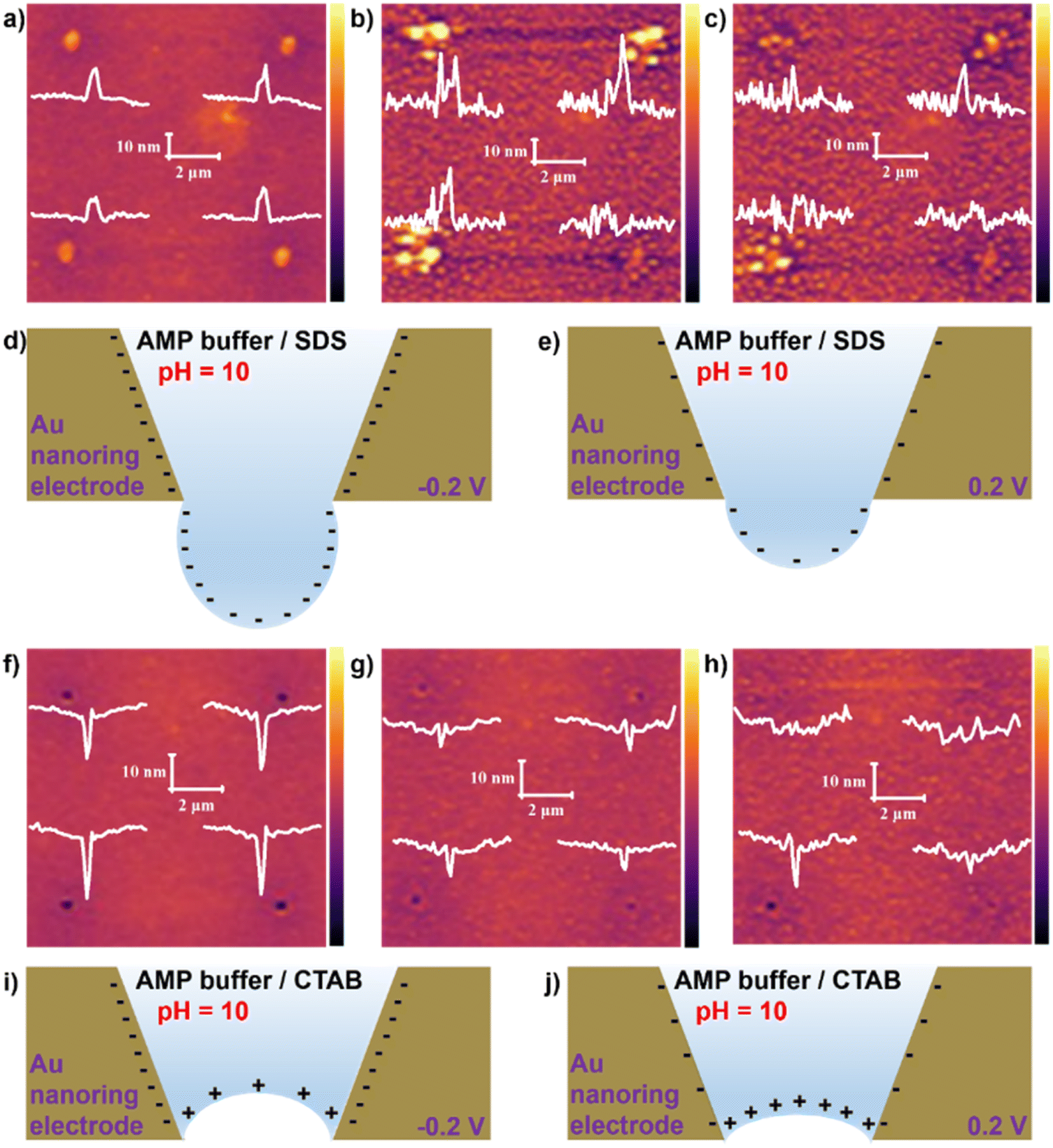 | ||
| Fig. 3 AFM characterization of the effect of surfactants on the nanointerfaces curvature in AMP buffers. AFM characterization of the nanointerfaces after the addition of (a–c) 40 μM SDS at (a) no potential, (b) −0.2 V, and (c) 0.2 V, and (f–h) CTAB at (f) no potential, (g) −0.2 V, and (h) 0.2 V; the insets show the specific height of each nanodroplet. Schematic of nanointerfaces subjected to electrostatic forces from Au nanoring electrodes after the addition of (d and e) SDS at (d) −0.2 V and (e) 0.2 V and (i and j) CTAB at (i) −0.2 V and (j) 0.2 V. | ||
A new nanointerface morphology, nanoconcave, an enantiomer of nanobubbles, can be observed with a CTAB-containing solution. Fig. 3F, S17A, and S17D† show the AFM characterization of nanointerface morphology in the AMP electrolyte with 40 μM of CTAB with no potential, showing nanoconcaves with a high degree of curvature. The open-circuit potential of gold in the buffer solution containing CTAB is −0.006 V vs. SHE (the calibration of gold is provided in Fig. S18†), which is more negative than the PZC of gold (+0.5 V vs. SHE), indicating that the gold electrode is negatively charged. The negative charges on the Au nanoring electrodes electrostatically attract the positive charges on the water–air interface. At −0.2 V vs. Ag QRE (−0.054 V vs. SHE), a nanoconcave morphology can also be obtained with an average depth of about 8 nm (Fig. 3G, S17B, and S17E†), which also resulted from the electrostatic attraction between the nanointerface and the electrode (Fig. 3I). The anomaly that the depth of the nanoconcaves in no potential case is more prominent than at −0.2 V might be due to the influence of electromigration.65,66 However, with +0.2 V applied (0.346 V vs. SHE), the curvature decreases (Fig. 3H, S17C, and S17F†), which is consistent with our theory (Fig. 3J).
The surfactant-modified nanointerfaces are further utilized for single-molecule detection. Fig. 4A shows fluorescence intensity versus time curves of imaging results (Fig. S19†) for Cy5.5 during the collision with different concentrations of SDS at pH 10 and −0.2 V. As the SDS concentration increased, the collision numbers between Cy5.5 and the water–air interface lowered. In this case, the dominant factor should be electrostatic repulsion between the negatively charged interface and the negatively charged molecules. The statistical results in Fig. 4C directly depict the negative correlation between SDS concentration and collision counts. Interestingly, with higher SDS concentration, the collision number increases with time. With high SDS concentration, the repulsion from the electrode could be stronger. The size of the nanodroplet is thus larger than the nanopore. For a spherical-shaped nanodroplet with a high surface negative charge, the diffusion layer67 could effectively exclude the negatively charged species within, resulting in a lower detection frequency of Cy5.5.
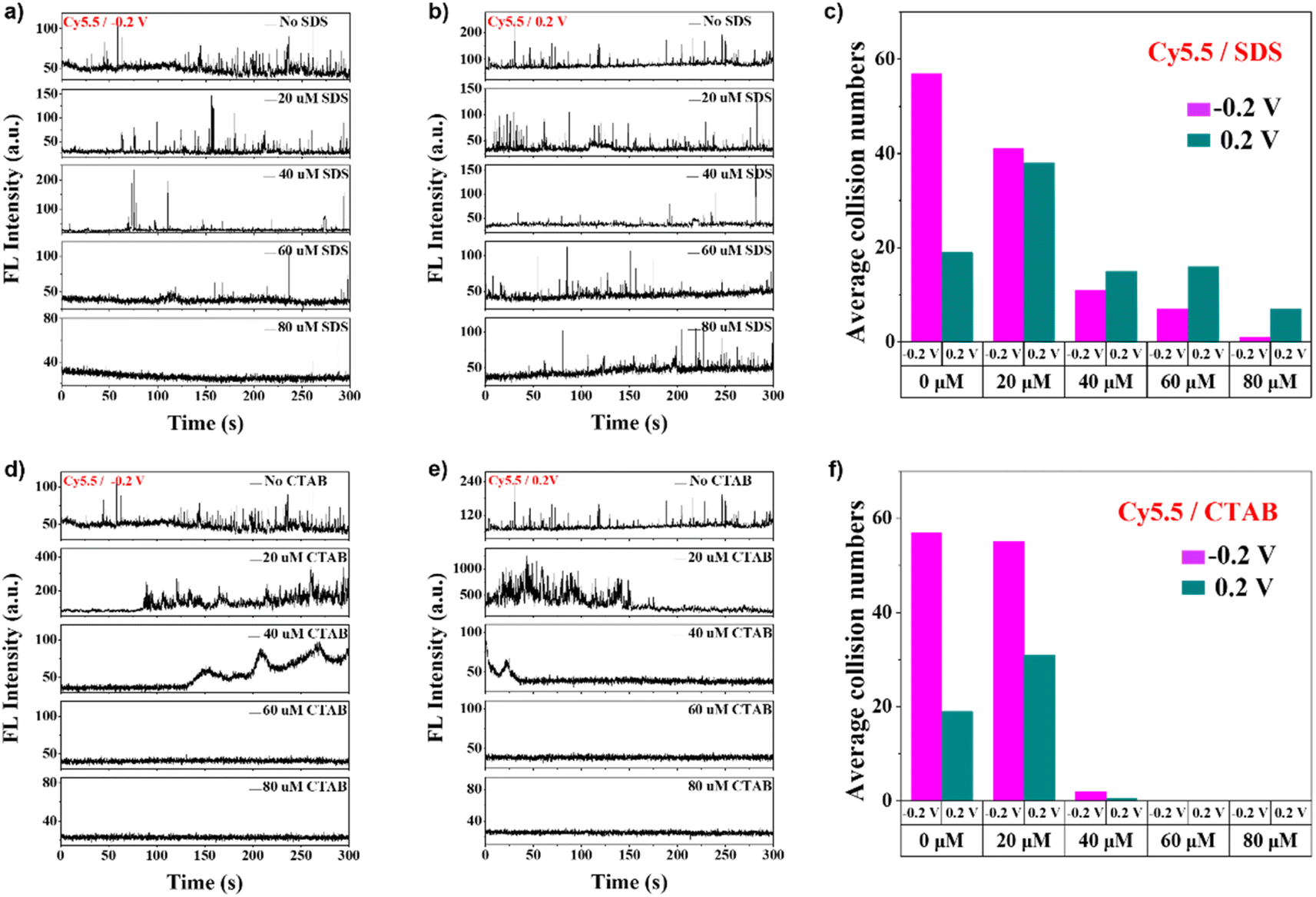 | ||
| Fig. 4 Collision of Cy5.5 with the water–air nanointerfaces in AMP buffers containing different surfactants at pH 10 and −0.2 V and 0.2 V. Fluorescence intensity versus time curves of Cy5.5 during the collisions with the nanointerfaces in the AMP buffers containing different concentrations of (a and b) SDS at (a) −0.2 V and (b) 0.2 V and (d and e) CTAB at (d) −0.2 V and (e) 0.2 V. Statistics of the average collision numbers of Cy5.5 with the nanointerfaces in the AMP buffers containing different concentrations of (c) SDS and (f) CTAB at −0.2 V and 0.2 V. Temporal continuity exists between −0.2 V and 0.2 V under the same conditions, where −0.2 V is applied first, followed by 0.2 V. | ||
The single-molecule collision behaviors of Cy5.5 with different concentrations of SDS at pH 10 and 0.2 V are shown in Fig. 4B and S20.† The collision numbers decrease as the SDS concentration increases (Fig. 4C). Unlike the monotonic decreases in collision numbers with increased concentration of SDS in the −0.2 V case, the collision counts peaked at 20 μM SDS, and the counts are significantly higher in more concentrated SDS solutions with +0.2 V applied. A temporal dependence of the collisions under this condition is not apparent. As shown in Fig. 3C, the diameters of the nanodroplets are similar to those of the nanopores. The electrostatic repulsion between the interface and the dyes should be the dominant factor for low collision frequency in high-concentration SDS solutions.
The nanoconcave is also used as a single-molecule detection platform. Fig. 4D, E, S22, and S23† show single-molecule collision behaviors of Cy5.5 in different concentrations of CTAB at pH 10 and at −0.2 V and +0.2 V. Due to the electric attraction between the CTAB-modified nanointerface and Cy5.5, with 20 μM CTAB, numerous collision events can be observed and become undistinguishable at an even higher concentration (40 μM). This is also clearly reflected in the statistical results of the average collision numbers in Fig. 4F. A significant temporal dependence of collision counts can be found in 20 μM and 40 μM CTAB solutions, with turning-on behaviors at −0.2 V and turning-off behaviors at +0.2 V. As mentioned above, a square wave was applied to the nanointerface before the recording. The temporal dependence should be due to the formation process of a stable water–air interface. The nanoconcave at −0.2 V should be a favorable water–air interface for dye insertion. In contrast, flatter ones at +0.2 V are not an ideal environment for such processes. The phenomena are similar to those in the case of no surfactant. The absence of detection (60 μM and 80 μM) should be due to the increased concavity of the interface into the nanopore, which blocks fluorescence detection.
Fig. 5A, B, S25, and S26† show single-molecule collision behaviors of +Cy5 in different concentrations of SDS at pH 10 and at −0.2 V and +0.2 V. As shown in the statistical results of the average collision numbers in Fig. 5C, the collision count at −0.2 V is slightly higher than that at 0.2 V. At the same time, the SDS concentration did not affect the collision events between +Cy5 and the water–air interface. This should be because the nanodroplets could not exclude dyes of opposite charges. The relatively low charge of +Cy5 makes insertion into charged water–air interfaces easier. The nanodroplets at −0.2 V are relatively larger (Fig. 3B and C), resulting in a slightly higher detection frequency.
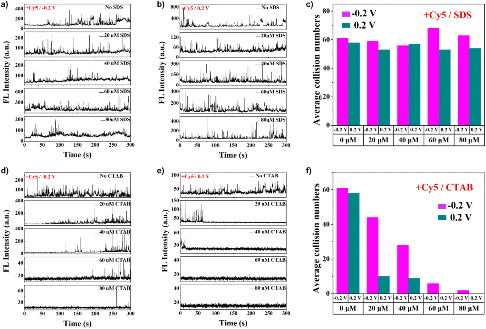 | ||
| Fig. 5 Collision of +Cy5 with the water–air nanointerfaces in AMP buffers containing different surfactants at pH 10 and −0.2 V and 0.2 V. Fluorescence intensity versus time curves of +Cy5 during the collisions with the nanointerfaces in the AMP buffers containing different concentrations of (a and b) SDS at (a) −0.2 V and (b) 0.2 V and (d and e) CTAB at (d) −0.2 V and (e) 0.2 V. Statistics of the average collision numbers of +Cy5 with the nanointerfaces in the AMP buffers containing different concentrations of (c) SDS and (f) CTAB at −0.2 V and 0.2 V. Temporal continuity exists between −0.2 V and 0.2 V under the same conditions, where −0.2 V is applied first, followed by 0.2 V. | ||
Fig. 5D, E, S28, and S29† show the single-molecule collision behaviors of +Cy5 in CTAB electrolyte solution (pH 10). Similar to the Cy5.5 situation, temporal-dependent collision behaviors can be observed. At −0.2 V, the collision events appear at later stages, and the on-set times are more delayed with higher CTAB concentration. In contrast, there are still collision events at higher concentrations of CTAB (60 and 80 μM). This is also reflected in the statistics of the average collision numbers in Fig. 5F. The temporal difference in collision behavior is similar to that in the previous situation. A more curved interface that favors single-molecule collision takes a particular time to be formed. The decreasing collision frequency with increased CTAB concentration should be due to electrostatic repulsion between the same positive charge of CATB and +Cy5.
Conclusion
In this study, a novel way to construct water–air interfaces was proposed, and the nanointerface properties were studied with single-molecule fluorescence. For the first time, AFM characterized the morphology of water–air nanointerfaces with diverse morphologies. The electrostatic interaction between the charged nanointerface and the electrodes, which the applied potentials can regulate, determines the curvature of the nanointerfaces: repulsion generates nanodroplets and attraction forms nanoconcaves. The nanointerfaces are probed by recording the collision behaviors of single fluorescent dyes, Cy5.5 (negatively charged) and +Cy5 (positively charged). The transient trapping of the single molecules during the collision could result in fluorescence bursts at the interface. SDS and CTAB were used to modify the surface charges of the interfaces further. An interesting phenomenon was unveiled that uncharged interfaces (at the isoelectric point) don't permit single-molecule insertion into the interfaces. A sufficient amount of charges at the interfaces, whether the same type or opposite, is necessary for collision behavior, although the electrostatic force might affect the collision frequency. Curved nanointerfaces instead of flat ones are preferred for single-molecule collisions. Stable water–air interfaces are constructed and studied with electrochemical regulation and single-molecule analysis. This study could help build next-generation single-molecule detection techniques as well as provide research means and theoretical support for water–air nanointerfaces for various applications in the fields of electrochemistry and energy.Data availability
The data supporting this article have been included as part of the ESI.†Author contributions
Guopeng Li and Lisi Wen contributed equally. GL conducted device fabrication and imaging experiments. LW collected AFM data. RS analyzed the data. RH conceived and supervised the project. GL wrote the manuscript. All authors contributed to the final version of the manuscript.Conflicts of interest
There are no conflicts to declare.Acknowledgements
This work was financially supported by the National Natural Science Foundation of China (22374064) and the Shenzhen Innovation of Science and Technology Commission (ZDSYS20230626090803004).References
- G. A. Novak and T. H. Bertram, Reactive VOC Production from Photochemical and Heterogeneous Reactions Occurring at the Air–Ocean Interface, Acc. Chem. Res., 2020, 53, 1014–1023 CrossRef CAS.
- F. Zhang, X.-Y. Yu and Z. Wang, Analytical advances to study the air – water interfacial chemistry in the atmosphere, Trends Environ. Anal. Chem., 2022, 36, e00182 CrossRef CAS.
- F. Niu, D. Wang, F. Li, Y. Liu, S. Shen and T. J. Meyer, Hybrid Photoelectrochemical Water Splitting Systems: From Interface Design to System Assembly, Adv. Energy Mater., 2019, 10, 1900399 CrossRef.
- Y. Du, B. Li, G. Xu and L. Wang, Recent advances in interface engineering strategy for highly-efficient electrocatalytic water splitting, InfoMat, 2022, 5, 12377 Search PubMed.
- A. J. Shih, M. C. O. Monteiro, F. Dattila, D. Pavesi, M. Philips, A. H. M. da Silva, R. E. Vos, K. Ojha, S. Park, O. van der Heijden, G. Marcandalli, A. Goyal, M. Villalba, X. Chen, G. T. K. K. Gunasooriya, I. McCrum, R. Mom, N. López and M. T. M. Koper, Water electrolysis, Nat. Rev. Methods Primers, 2022, 2, 84 CrossRef CAS.
- J. Li, L. Ding, Z. Su, K. Li, F. Fang, R. Sun, Y. Qin and K. Chang, Non-Lignin Constructing the Gas–Solid Interface for Enhancing the Photothermal Catalytic Water Vapor Splitting, Adv. Mater., 2023, 35, 2305535 CrossRef CAS PubMed.
- V. R. Stamenkovic, D. Strmcnik, P. P. Lopes and N. M. Markovic, Energy and fuels from electrochemical interfaces, Nat. Mater., 2016, 16, 57–69 CrossRef PubMed.
- J. Filippi, L. Rotundo, R. Gobetto, H. A. Miller, C. Nervi, A. Lavacchi and F. Vizza, Turning manganese into gold: efficient electrochemical CO2 reduction by a fac-Mn(apbpy)(CO)3Br complex in a gas–liquid interface flow cell, Chem. Eng. J., 2021, 416, 129050 CrossRef CAS.
- J. Dong, J. Chen, W. Wang, Z. Wei, Z.-Q. Tian and F. R. Fan, Charged Microdroplets as Microelectrochemical Cells for CO2 Reduction and C–C Coupling, J. Am. Chem. Soc., 2024, 146, 2227–2236 CrossRef CAS.
- J. Yu, B. Q. Li, C. X. Zhao, J. N. Liu and Q. Zhang, Asymmetric Air Cathode Design for Enhanced Interfacial Electrocatalytic Reactions in High-Performance Zinc–Air Batteries, Adv. Mater., 2020, 32, 1908488 CAS.
- S. Lu, Y. Wang, H. Xiang, H. Lei, B. B. Xu, L. Xing, E. H. Yu and T. X. Liu, Mass transfer effect to electrochemical reduction of CO2: electrode, electrocatalyst and electrolyte, J. Energy Storage, 2022, 52, 104764 Search PubMed.
- L. Zhang, Y. Zhang, X. Zhang, Z. Li, G. Shen, M. Ye, C. Fan, H. Fang and J. Hu, Electrochemically Controlled Formation and Growth of Hydrogen Nanobubbles, Langmuir, 2006, 22, 8109–8113 CAS.
- S. Yang, P. Tsai, E. S. Kooij, A. Prosperetti, H. J. W. Zandvliet and D. Lohse, Electrolytically Generated Nanobubbles on Highly Orientated Pyrolytic Graphite Surfaces, Langmuir, 2009, 25, 1466–1474 CAS.
- E. Dollekamp, P. Bampoulis, B. Poelsema, H. J. Zandvliet and E. S. Kooij, Electrochemically Induced Nanobubbles between Graphene and Mica, Langmuir, 2016, 32, 6582–6590 CAS.
- Q. J. Chen and L. Luo, Correlation between Gas Bubble Formation and Hydrogen Evolution Reaction Kinetics at Nanoelectrodes, Langmuir, 2018, 34, 4554–4559 CAS.
- L. Luo and H. S. White, Electrogeneration of Single Nanobubbles at Sub-50-nm-Radius Platinum Nanodisk Electrodes, Langmuir, 2013, 29, 11169–11175 CAS.
- Q. J. Chen, L. Luo, H. Faraji, S. W. Feldberg and H. S. White, Electrochemical Measurements of Single H2 Nanobubble Nucleation and Stability at Pt Nanoelectrodes, J. Phys. Chem. Lett., 2014, 5, 3539–3544 CrossRef CAS.
- Q. J. Chen, H. S. Wiedenroth, S. R. German and H. S. White, Electrochemical Nucleation of Stable N2 Nanobubbles at Pt Nanoelectrodes, J. Am. Chem. Soc., 2015, 137, 12064–12069 CrossRef CAS.
- S. R. German, M. A. Edwards, Q. J. Chen, Y. W. Liu, L. Luo and H. S. White, Electrochemistry of single nanobubbles. Estimating the critical size of bubble-forming nuclei for gas-evolving electrode reactions, Faraday Discuss., 2016, 193, 223–240 RSC.
- H. Ren, S. R. German, M. A. Edwards, Q. Chen and H. S. White, Electrochemical Generation of Individual O2 Nanobubbles via H2O2 Oxidation, J. Phys. Chem. Lett., 2017, 8, 2450–2454 CrossRef CAS PubMed.
- S. R. German, M. A. Edwards, H. Ren and H. S. White, Critical Nuclei Size, Rate, and Activation Energy of H2 Gas Nucleation, J. Am. Chem. Soc., 2018, 140, 4047–4053 CrossRef CAS PubMed.
- M. A. Edwards, H. S. White and H. Ren, Voltammetric Determination of the Stochastic Formation Rate and Geometry of Individual H2, N2, and O2 Bubble Nuclei, ACS Nano, 2019, 13, 6330–6340 CrossRef CAS PubMed.
- Q. J. Chen, Y. W. Liu, M. A. Edwards, Y. L. Liu and H. S. White, Nitrogen Bubbles at Pt Nanoelectrodes in a Nonaqueous Medium: Oscillating Behavior and Geometry of Critical Nuclei, Anal. Chem., 2020, 92, 6408–6414 CrossRef CAS.
- S. Karpitschka, E. Dietrich, J. R. T. Seddon, H. J. W. Zandvliet, D. Lohse and H. Riegler, Nonintrusive Optical Visualization of Surface Nanobubbles, Phys. Rev. Lett., 2012, 109, 0066102 CrossRef PubMed.
- R. Hao, Y. S. Fan, M. D. Howard, J. C. Vaughan and B. Zhang, Imaging nanobubble nucleation and hydrogen spillover during electrocatalytic water splitting, Proc. Natl. Acad. Sci. U.S. A., 2018, 115, 5878–5883 CrossRef CAS PubMed.
- R. Hao, Y. Fan, T. J. Anderson and B. Zhang, Imaging Single Nanobubbles of H2 and O2 During the Overall Water Electrolysis with Single-Molecule Fluorescence Microscopy, Anal. Chem., 2020, 92, 3682–3688 CrossRef CAS PubMed.
- Z. Y. Peng and B. Zhang, Nanobubble Labeling and Imaging with a Solvatochromic Fluorophore Nile Red, Anal. Chem., 2021, 93, 15315–15322 CrossRef CAS PubMed.
- M. Suvira and B. Zhang, Effect of Surfactant on Electrochemically Generated Surface Nanobubbles, Anal. Chem., 2021, 93, 5170–5176 CrossRef CAS PubMed.
- W. R. Leininger, Z. Peng and B. Zhang, Transient Adsorption Behavior of Single Fluorophores on an Electrode-Supported Nanobubble, Chem. Biomed. Imaging, 2023, 1, 380–386 CrossRef CAS PubMed.
- H. Su, Y. Fang, F. Chen and W. Wang, Monitoring the dynamic photocatalytic activity of single CdS nanoparticles by lighting up H2 nanobubbles with fluorescent dyes, Chem. Sci., 2018, 9, 1448–1453 RSC.
- H. Xu and X. Zhang, Formation, characterization and stability of oil nanodroplets on immersed substrates, Adv. Colloid Interface Sci., 2015, 224, 17–32 CrossRef CAS PubMed.
- D. Lohse and X. Zhang, Surface nanobubbles and nanodroplets, Rev. Mod. Phys., 2015, 87, 981–1035 CrossRef CAS.
- E. Lim, B. Kim, M. S. Oh and J. B. You, Microfluidic formation of surface nanodroplets using green deep eutectic solvents for liquid–liquid nanoextraction and controlled precipitation, J. Colloid Interface Sci., 2023, 643, 82–91 CrossRef CAS PubMed.
- J. B. You, Surface nanodroplets as platforms for small scale chemical engineering, Chem. Eng. J., 2024, 483, 149252 CrossRef CAS.
- W. Huang, L. Zhao, X. He, Y. Li, C. P. Collier, Z. Zheng, J. Liu, D. P. Briggs and J. Cheng, Low-temperature Leidenfrost-like jumping of sessile droplets on microstructured surfaces, Nat. Phys., 2024, 20, 1274–1281 Search PubMed.
- Y.-H. Tsao, T.-Y. Wang, H.-K. Tsao and Y.-J. Sheng, Thermally assisted mobility of nanodroplets on surfaces with weak defects, J. Colloid Interface Sci., 2021, 604, 150–156 CAS.
- D. Valavanis, P. Ciocci, I. J. McPherson, G. N. Meloni, J.-F. Lemineur, F. Kanoufi and P. R. Unwin, Operando Electrochemical and Optical Characterization of the Meniscus of Scanning Electrochemical Cell Microscopy (SECCM) Probes, ACS Electrochem., 2025, 1, 153–163 CrossRef CAS PubMed.
- Y. L. Ying, J. J. Wang, A. R. Leach, Y. Jiang, R. Gao, C. Xu, M. A. Edwards, A. D. Pendergast, H. Ren, C. K. T. Weatherly, W. Wang, P. Actis, L. Q. Mao, H. S. White and Y. T. Long, Single-entity electrochemistry at confined sensing interfaces, Sci. China Chem., 2020, 63, 589–618 CAS.
- H. Zhao, J. Ma, X. Zuo and F. Li, Electrochemical Analysis for Multiscale Single Entities on the Confined Interface, Chin. J. Chem., 2021, 39, 1745–1752 CAS.
- X. Li, Y. H. Fu, N. Wei, R. J. Yu, H. Bhatti, L. Zhang, F. Yan, F. Xia, A. G. Ewing, Y. T. Long and Y. L. Ying, Emerging Data Processing Methods for Single-Entity Electrochemistry, Angew. Chem., Int. Ed., 2024, 63, e202316551 CAS.
- A. M. El-Aziz, L. A. Kibler and D. M. Kolb, The potentials of zero charge of Pd(111) and thin Pd overlayers on Au(111), Electrochem. Commun., 2002, 4, 535–539 CAS.
- J. B. Le, M. Iannuzzi, A. Cuesta and J. Cheng, Determining Potentials of Zero Charge of Metal Electrodes versus the Standard Hydrogen Electrode from Density-Functional-Theory-Based Molecular Dynamics, Phys. Rev. Lett., 2017, 119, 016801 Search PubMed.
- H. Iyota and R. Krastev, Equilibrium thickness of foam films and adsorption of ions at surfaces: water and aqueous solutions of sodium chloride, hydrochloric acid, and sodium hydroxide, J. Colloid Interface Sci., 2020, 565, 405–415 CAS.
- V. P. Carey, Surface Tension Effects on Post-Nucleation Growth of Water Microdroplets in Supersaturated Gas Mixtures, J. Heat Transfer, 2000, 122, 294–302 CrossRef CAS.
- S. Fan, J. E. A. Webb, Y. Yang, D. J. Nieves, V. R. Gonçales, J. Tran, G. Hilzenrat, M. Kahram, R. D. Tilley, K. Gaus and J. J. Gooding, Observing the Reversible Single Molecule Electrochemistry of Alexa Fluor 647 Dyes by Total Internal Reflection Fluorescence Microscopy, Angew. Chem., Int. Ed., 2019, 58, 14495–14498 CrossRef CAS PubMed.
- Y. Yang, Y. Ma, J. F. Berengut, L. K. Lee, R. D. Tilley, K. Gaus and J. J. Gooding, Electrochemically controlled blinking of fluorophores for quantitative STORM imaging, Nat. Photonics, 2024, 18, 713–720 CrossRef CAS.
- Y. Yang, Y. Ma and J. J. Gooding, The electrochemical modulation of single molecule fluorescence, Faraday Discuss., 2025, 257, 333–343 RSC.
- H. He and R. Hao, Multiplexed Fluoro-electrochemical Single-Molecule Counting Enabled by SiC Semiconducting Nanofilm, Nano Lett., 2024, 24, 11051–11058 Search PubMed.
- J. Lu, Y. Fan, M. D. Howard, J. C. Vaughan and B. Zhang, Single-Molecule Electrochemistry on a Porous Silica-Coated Electrode, J. Am. Chem. Soc., 2017, 139, 2964–2971 Search PubMed.
- N. O. Mchedlov-Petrossyan, A. Y. Kharchenko, M. O. Marfunin and O. R. Klochaniuk, Nano-sized bubbles in solution of hydrophobic dyes and the properties of the water/air interface, J. Mol. Liq., 2019, 275, 384–393 CrossRef CAS.
- Y. Gu and D. Li, Measurements of the electric charge and surface potential on small aqueous drops in the air by applying the Millikan method, Colloids Surf. A: Physicochem. Eng., 1998, 137, 205–215 CrossRef CAS.
- M. Manciu and E. Ruckenstein, Ions near the air/water interface. II: Is the water/air interface acidic or basic? Predictions of a simple model, Colloids Surf. A: Physicochem. Eng., 2012, 404, 93–100 CrossRef CAS.
- O. Stern, Zur Theorie Der Elektrolytischen Doppelschicht, Z. Elektrochem. Angew. Phys. Chem., 2014, 30, 508–516 Search PubMed.
- X. Shi, J. Xie, F. Yang, F. Wang, D. Zheng, X. Cao, Y. Yu, Q. Liu and X. Lu, Compacting Electric Double Layer Enables Carbon Electrode with Ultrahigh Zn Ion Storage Capability, Angew. Chem., Int. Ed., 2022, 61, e202214773 CrossRef CAS PubMed.
- J. Hu, M. Iwamoto and X. Chen, A Review of Contact Electrification at Diversified Interfaces and Related Applications on Triboelectric Nanogenerator, Nanomicro Lett., 2023, 16, 7–31 Search PubMed.
- D. Li, Z. Yang, A. A. Pahlavan, R. Zhang, R. Hu and Y.-F. Chen, Stability Transition in Gap Expansion-Driven Interfacial Flow, Phys. Rev. Lett., 2024, 133, 034003 CrossRef CAS PubMed.
- S. Huang, P. Lv and H. Duan, Morphology evolution of liquid–gas interface on submerged solid structured surfaces, Extreme Mech. Lett., 2019, 27, 34–51 CrossRef.
- V. Metelev, R. Weissleder and A. Bogdanov, Synthesis and Properties of Fluorescent NF-κB-Recognizing Hairpin Oligodeoxyribonucleotide Decoys, Bioconjugate Chem., 2004, 15, 1481–1487 CrossRef CAS.
- T. Ma, Y. Hou, J. Zeng, C. Liu, P. Zhang, L. Jing, D. Shangguan and M. Gao, Dual-Ratiometric Target-Triggered Fluorescent Probe for Simultaneous Quantitative Visualization of Tumor Microenvironment Protease Activity and pH in Vivo, J. Am. Chem. Soc., 2017, 140, 211–218 CrossRef.
- H. A. Shindy, Fundamentals in the chemistry of cyanine dyes: a review, Dyes Pigm., 2017, 145, 505–513 CrossRef CAS.
- G. Zhang and M. Schreier, Leveraging electrochemical double layer structure to rationally control electrolysis, Natl. Sci. Rev., 2024, 11, nwae299 CrossRef.
- A. Sharipova, S. Aidarova, V. B. Fainerman, A. Stocco, P. Cernoch and R. Miller, Dynamics of adsorption of polyallylamine hydrochloride/sodium dodecyl sulphate at water/air and water/hexane interfaces, Colloids Surf. A: Physicochem. Eng., 2011, 391, 112–118 CrossRef CAS.
- T. Adel, K. C. Ng, M. G. Vazquez de Vasquez, J. Velez-Alvarez and H. C. Allen, Insight into the Ionizing Surface Potential Method and Aqueous Sodium Halide Surfaces, Langmuir, 2021, 37, 7863–7874 CrossRef CAS PubMed.
- M. Suvira and B. Zhang, Single-Molecule Interactions at a Surfactant-Modified H2 Surface Nanobubble, Langmuir, 2021, 37, 13816–13823 CrossRef CAS PubMed.
- H. L. Huang and J. S. Yang, Summary Abstract: Surface morphology and electromigration, J. Vac. Sci. Technol. A: Vac. Surf. Films, 1987, 5, 1487–1488 CrossRef.
- R. Sprocati and M. Rolle, On the interplay between electromigration and electroosmosis during electrokinetic transport in heterogeneous porous media, Water Res., 2022, 213, 118161 CrossRef CAS.
- J. Wu, Understanding the Electric Double-Layer Structure, Capacitance, and Charging Dynamics, Chem. Rev., 2022, 122, 10821–10859 CrossRef CAS PubMed.
Footnotes |
| † Electronic supplementary information (ESI) available. See DOI: https://doi.org/10.1039/d5sc00189g |
| ‡ These authors contributed equally. |
| This journal is © The Royal Society of Chemistry 2025 |