Photo- and electroactive amorphous molecular materials—molecular design, syntheses, reactions, properties, and applications
Yasuhiko
Shirota
ab
aCenter for Advanced Science and Innovation, Osaka University, Yamadaoka, Suita, Osaka 565-0871, Japan. E-mail: shirota@ap.chem.eng.osaka-u.ac.jp
bFukui University of Technology, 3-6-1, Gakuen, Fukui City, Fukui 910-8505, Japan
First published on 24th November 2004
Abstract
A new field of organic materials science that deals with amorphous molecular glasses has been opened up. In addition, amorphous molecular materials have constituted a new class of functional organic materials for use in various applications. This article is focused on the recent progress of studies on photo- and electroactive amorphous molecular materials, highlighting photochromic amorphous molecular materials, amorphous molecular resists, and amorphous molecular materials for use in devices such as organic EL devices. The molecular design concepts, syntheses, reactions, molecular and solid-state properties, functions, and device fabrication and performance are described.
 Yasuhiko Shirota |
Yasuhiko Shirota graduated from Osaka University in 1963, and received his Doctor of Engineering from Osaka University in 1968. He was appointed to be a Research Associate at Osaka University in 1968 and promoted to an Associate Professor in 1972, and a Professor in 1986. Since 2003, he has been a Professor Emeritus of Osaka University, a Guest Professor at Center for Advanced Science and Innovation, Osaka University, and a Professor at Fukui University of Technology. His research interest covers a wide field of organic materials science including the synthesis, structures, reactions, properties, functions, and device performance of both small organic molecules and polymers. He received The Society of Polymer Science Japan Award in 1980 and The Chemical Society of Japan Award in 1999. |
1 Introduction
Control over materials morphology is a key issue in materials science and practical applications. Among several organisation states, e.g., single crystals, polycrystals, liquid crystals, and amorphous glasses, amorphous glasses are good candidates for materials for various applications because of their good processability, transparency, and homogeneous properties. Amorphous metals and inorganic amorphous glasses have recently attracted a great deal of attention as a new class of materials. With regard to organic materials, amorphous polymers and composite polymer systems in which small molecules are dispersed are well known. Small organic molecules, on the other hand, generally tend to crystallise very readily, and hence, they usually exist as crystals below their melting temperatures. However, recent extensive studies have revealed that small organic molecules can also form stable amorphous glasses above room temperature if their molecular structures are properly designed.1 Small organic molecules that readily form stable amorphous glasses above room temperature are referred to as “amorphous molecular materials”.Amorphous molecular materials are of interest because of the following aspects.1 They are in a state of thermodynamic nonequilibrium and hence, they undergo structural relaxation, exhibiting glass-transition phenomena usually associated with amorphous polymers. They can assume several different organisation states, e.g., amorphous glass, crystal, supercooled liquid, and melt. They show isotropic and homogeneous properties without grain boundaries. They are characterised by the presence of free volume and disorder in both molecular distance and orientation. They are capable of forming uniform amorphous thin films by themselves by either vacuum deposition or spin coating from solution.
Amorphous molecular materials have received growing attention, in particular, from the standpoint of application as materials for organic electroluminescent (EL) devices, and a number of reports have been published since the mid-1990s. A new field of organic materials science that deals with amorphous molecular glasses has now been opened up. In addition, amorphous molecular materials have constituted a new class of functional organic materials for use in various applications.
Since the late 1980s, we have performed a series of studies on the creation of amorphous molecular materials and have investigated their structures, reactions, properties, functions, and applications.1 We aimed at creating amorphous molecular materials based on π-electron systems in light of their characteristic features, e.g., UV and visible light absorption and emission, charge carrier generation and transport, and nonlinear optical properties.
This article is focused on the recent progress of studies on photo- and electroactive amorphous molecular materials, highlighting photochromic amorphous molecular materials, amorphous molecular resists, and amorphous molecular materials for use in devices such as organic EL devices. The molecular design concepts, syntheses, reactions, molecular and solid-state properties, functions, and device fabrication and performance are described.
2 Molecular design concepts and creation of amorphous molecular materials
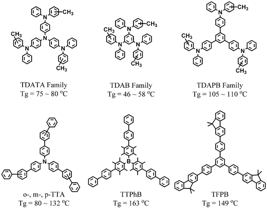
Studies of the correlation between molecular structures and glass-forming properties, glass-transition temperatures, and the stability of the glassy state have provided several important guidelines for the molecular design of amorphous molecular materials.1 (1) Molecules should possess nonplanar molecular structures, as evidenced by their X-ray crystal structure analysis. (2) Nonplanar molecular structures, however, do not necessarily lead to the formation of amorphous glasses. The existence of different conformers in addition to nonplanar molecular structures is required for the formation of amorphous glasses. (3) The incorporation of bulky and heavy substituents makes glass formation easier, leading to enhanced stability of the resulting amorphous glasses. (4) The enlargement of molecular size also enhances the stability of the glassy state. (5) The glass-transition temperature (Tg) can be increased by the introduction of structurally rigid moieties, e.g., biphenyl, naphthalene, fluorene, carbazole, and phenothiazine, and by the introduction of heavy substituents. (6) Tg also increases with increasing molecular size and weight.A variety of amorphous molecular materials based on π-electron systems have been created. Typical key compounds that form amorphous glasses are the following: π-electron starburst molecules, e.g., the families of tris(diphenylamino)triphenylamine (TDATA),2 1,3,5-tris(diphenylamino)benzene (TDAB),3 and 1,3,5-tris[4-(diphenylamino)phenyl]benzene (TDAPB),4 diarylaminophenylaldehyde arylhydrazones,5 tris(oligoarylenyl)amines, e.g., tri(terphenyl-4-yl)amine (p-TTA),6 1,3,5-triarylbenzenes,7,8 tris(oligoarylenyl)boranes,9 a variety of triarylamine end-capped π-electron systems,10,11 molecules containing macrocyclic rings such as phthalocyanine12 and porphyrin13 cores, e.g., PcArA and PorArA, spiro-compounds, e.g., Spiro-4Φ14 and tetraarylmethane derivatives, e.g., C(tBuSSB)4.15 A number of amorphous molecular materials with various structural modifications of the above key compounds have also been reported. The modifications include the replacement of a phenyl group by a naphthyl, fluorenyl, phenanthryl, or oxadiazoyl group, the replacement of a diphenylamino group by a carbazolyl or benzocarbazolyl group, and the enlargement of the molecular size to form dendrimers. Examples of such materials are described later.
TDATA and methyl-substituted TDATA have been synthesised by the Ullmann coupling reaction of tris(4-iodophenyl)amine with diphenylamine or methyl-substituted diphenylamine. TDAB and methyl-substituted TDAB have been synthesised by the reaction of phloroglucinol with aniline, followed by the Ullmann coupling reaction with iodobenzene or methyl-substituted iodobenzene. TDAPB and methyl-substituted TDAPB have been synthesised by the Ullmann coupling reaction between 1,3,5-tris(4-iodophenyl)benzene and diphenylamine or methyl-substituted diphenylamine. p-TTA has been synthesized by the Grignard coupling reaction of tris(4-iodophenyl)amine with biphenyl-4-yl magnesium bromide. It can also be prepared by the Suzuki coupling reaction using biphenyl-4-yl boronic acid.
The formation of the amorphous glassy state is confirmed by polarising microscopy, X-ray diffraction (XRD), differential scanning calorimetry (DSC), and Raman spectroscopy.1 Amorphous molecular materials contrast polymers in that they are pure materials with well-defined molecular structures and definite molecular weights without any distribution, and can be purified mostly by column chromatography, followed by recrystallisation from solution or by vacuum sublimation. Many of the compounds have been obtained as polycrystals by recrystallisation from solution. They readily form amorphous glasses when the melt samples are cooled on standing in air or rapidly cooled with liquid nitrogen. The stability of the resulting amorphous glasses greatly depends on molecular structures. Stable amorphous glasses that do not undergo crystallisation even on heating above their Tgs have also been created. Some compounds have been obtained only as amorphous glasses despite attempted recrystallisation from solution.
Amorphous molecular materials are characterised by well-defined Tgs and ready formation of uniform amorphous thin films by themselves. Tg is a key factor that determines the thermal stability of amorphous molecular materials. The Tg of amorphous molecular glasses is understood as the temperature at which molecular motions of a group of molecules begin to take place, resulting in the change in the gravity of molecules and being accompanied by a specific heat change.
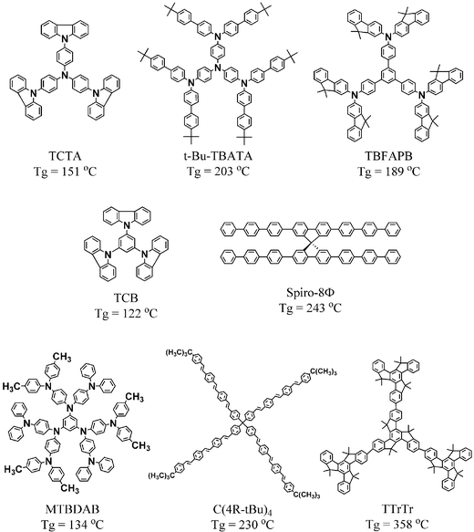
Thermally stable amorphous molecular materials have been developed on the basis of the ideas of incorporating rigid moieties and enlarging the molecular size. The examples are given by e.g., 4,4′,4″-tris(N-carbazolyl)triphenylamine (TCTA),16 4,4′,4″-tris[bis(4′-tert-butylbiphenyl-4-yl)amino]triphenylamine (t-Bu-TBATA),17 1,3,5-tris{4-[bis(9,9-dimethyl-fluoren-2-yl)amino]phenyl}benzene (TBFAPB),18 1,3,5-tris(N-carbazolyl)benzene,19 spiro-8Φ,14 2,7,12-tris(5,5,10,10,15,15-hexamethyltruxen-2-yl)-5,5,10,10,15,15-hexamethyltruxene (TTrTr),20 and dendrimers, e.g., MTBDAB21 and others.22 An attempt to increase the Tg of amorphous molecular materials tends to make materials insoluble and unprocessable. It is required to develop soluble, processable materials with high Tgs. A truxene-based amorphous molecular material TTrTr exhibited a Tg of 358 °C, which is the highest ever reported for soluble, processable amorphous molecular materials.20
It is of great interest to provide amorphous molecular materials with various functions. We have proposed several novel concepts for photo- and electroactive organic materials, which include electrically conducting amorphous molecular materials,23 photochromic amorphous molecular materials,11 and amorphous molecular resists.24 In addition, amorphous molecular materials have demonstrated their suitability and versatility as photo- and electroactive materials for electronic, optoelectronic, and photonic devices, in particular, organic EL devices or organic light-emitting diodes (OLEDs) (Fig. 1).
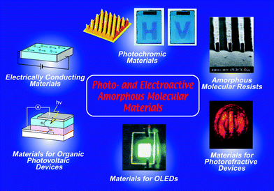 | ||
| Fig. 1 Photo- and electroactive amorphous molecular materials. | ||
3 Photochromic amorphous molecular materials
Photochromic materials have recently attracted renewed interest in view of their potential technological applications for optical data storage and optical switching. Since such applications usually require materials as solid films, there have been extensive studies on photochromic polymers and molecularly dispersed polymer systems, where small organic photochromic molecules are dispersed in a polymer binder.25–27Photochromic amorphous molecular materials constitute a new class of photochromic materials that form uniform amorphous films by themselves. They have an advantage over polymers and molecularly dispersed polymer systems, where small molecules may crystallise at high concentrations, in that there is no dilution of photochromic chromophores.11
3-1 Creation of photochromic amorphous molecular materials
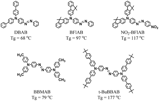
Considering that the photochromic behaviour of azobenzenes have been studied extensively and that dithienylethenes are known as fatigue-resistant, thermally stable photochromic compounds, we have created photochromic amorphous molecular materials based on azobenzene and dithienylethene chromophores.11,28–33 The synthesised azobenzene-based compounds include 4-[bis(4-methylphenyl)amino]azobenzene (BMAB), 4-[bis(4-methylphenyl)amino]-4′-methoxyazobenzene (MeO-BMAB), 4-[di(biphenyl-4-yl)amino]azobenzene (DBAB), 4-[bis(9,9-dimethylfluoren-2-yl)amino]azobenzene (BFlAB), 4-[bis(9,9-dimethylfluoren-2-yl)amino]-4′-nitroazobenzene (BFlAB-NO2), 4,4′-bis[bis(4-methylphenyl)amino]azobenzene (BBMAB), and 4,4′-bis[bis(4′-tert-butylbiphenyl-4-yl)amino]azobenzene (t-BuBBAB).11,28,29,32,33 BFlAB was synthesised by the Ullmann coupling reaction of 4-aminoazobenzene with 2-iodo-9,9-dimethylfluorene. Dithienylethene-based compounds include 1-{5-[4-(di-p-tolylamino)phenyl]-2-methylthiophen-3-yl}-2-(2,5-dimethylthiophen-3-yl)-3,3,4,4,5,5-hexafluorocyclopentene (TPTTC), 1-(5-{4-[bis(4-methylphenyl)amino]phenyl}-2-methylthiophen-3-yl)-2-(2-methylbenzo[b]thiophen-3-yl)-3,3,4,4,5,5-hexafluorocyclopentene (TPTBC), and 1,2-bis(5-{4-[bis(4-methylphenyl)amino]phenyl}-2-methylthiophen-3-yl)-3,3,4,4,5,5-hexafluorocyclopentene (BTPTC).30,31All these compounds readily formed amorphous glasses with well-defined Tgs when the melt samples were cooled on standing in air. Tg increased with the increasing molecular size, with the introduction of rigid moieties, e.g., biphenyl and fluorenyl groups, and with the introduction of polar substituents. They formed uniform amorphous films by spin coating from solution.
All the compounds described above were found to exhibit photochromism as amorphous films as well as in solution. Upon irradiation of amorphous films of the azobenzene-based compounds with 450 nm light, photoisomerisation from the trans-form to the cis-form took place. When irradiation was stopped after the reaction system had reached the photostationary state, the backward thermal isomerisation from the cis-form to the trans-form took place. The backward cis–trans isomerisation also took place by irradiation with 500 nm light. The fractions of the photogenerated cis-isomers at the photostationary state as amorphous film were found to be smaller than those in solution (0.81–0.85 in solution and 0.53–0.54 as amorphous films for BMAB, DBAB, and BFlAB), significantly decreasing with the increasing molecular size, and in particular, with the introduction of a diarylamino group at the two phenyl groups of the azobenzene chromophore (0.80 in solution and 0.17 and 0.15 as amorphous films for BBMAB and t-BuBBAB, respectively). These results suggest that the local free volume of amorphous films is not large enough for the whole molecules to be isomerised.11,34
As it is thought that reactions as amorphous films are affected by the surroundings, studies of reactions as amorphous films are expected to provide information about the microstructures of amorphous films. The cis–trans thermal isomerisation reactions of azobenzene-based amorphous molecular materials as amorphous films were found to exhibit the following features.11,32,33 While the backward thermal isomerisation reaction from the photogenerated cis-form to the trans-form in solution followed first-order kinetics for all the compounds described above, the reaction as amorphous films did not follow first-order kinetics, and the apparent reaction rate as amorphous films was found to be either accelerated or retarded relative to that in solution, depending upon the molecular structures. As Fig. 2a shows, the apparent rate constant for the thermal isomerisation of BMAB, DBAB, and BFlAB as amorphous films was initially larger than that in solution, gradually approaching that of the reaction in solution. The reactions as amorphous films could be analysed in terms of the first-order kinetics consisting of two components: fast and slow. The apparent rate constants of the fast component were approximately two orders of magnitude greater than those of the slow component, which were almost the same as those in solution. These results suggest that there exist cis-isomers trapped in constrained conformations as amorphous films, which go back faster to the trans-isomers than the structurally relaxed cis-isomers.11,32,33 On the other hand, the apparent rate constants for the thermal isomerisation reactions of BBMAB and t-BuBBAB as amorphous films were significantly smaller than those in solution, as shown in Fig. 2b. BBMAB and t-BuBBAB were found to be much more reactive than DBAB and BFlAB, and the first-order rate constants for the cis–trans isomerisation in solution were approximately two orders of magnitude larger than those for DBAB and BFlAB. However, the reaction of BBMAB as amorphous film was much slower than the reaction in solution, although the apparent rate constant for BBMAB as amorphous film was approximately one order of magnitude larger than those of DBAB and BFlAB as amorphous films. It is thought that the free volume is not large enough to readily allow the cis–trans isomerisation as amorphous film. The photogenerated cis-form of t-BuBBAB as amorphous film was fairly stable at room temperature.11
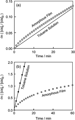 | ||
| Fig. 2 First order plots of cis–trans isomerization of (a) DBAB and (b) BBMAB in toluene solution and as amorphous films. | ||
It is noteworthy that the acceleration effect of the cis–trans thermal isomerisation observed for e.g., BFlAB, became more prominent when irradiation was stopped before the reaction system reached the photostationary state. The analysis of the reaction in terms of the first-order kinetics consisting of the two components showed that the fraction of the faster component significantly increased with decreasing irradiation time. It is understood that the local free volume around the molecules as amorphous films as prepared is not large, and hence, the relative ratio of strained cis-isomers to structurally relaxed ones is initially higher; however, the local free volume is gradually enlarged during repeated trans–cis and cis–trans photoisomerisations that accompany changes in the molecular shape. Consequently, the fraction of the faster component gradually decreases with increasing irradiation time, reaching that of the photostationary state.34
Dithienylethene-based photochromic amorphous molecular materials also exhibited photochromism as amorphous films as well as in solution.30,31 Upon irradiation of spin-coated amorphous film of the open-form of BTPTC (BTPTC-o) with 365 nm light, the band with a maximum at around 360 nm gradually decreased, and new absorption bands with maxima at around 442 and 635 nm together with a shoulder at ∼675 nm appeared as a result of the transformation of BTPTC-o to its cyclised isomer (BTPTC-c), and the reaction system reached the photostationary state (Fig. 3). The backward ring-opening reaction of BTPTC-c to regenerate BTPTC-o took place by irradiation with visible light of wavelength longer than 580 nm. The quantum yields for the photocyclisation of TPTTC, TPTBC, and BTPTC were higher (0.81, 0.79, and 0.61, respectively, in solution, and 0.28, 0.33, and 0.61 as amorphous films) than those reported for other dithienylethene derivatives that do not form amorphous glasses (mostly in the range from 0.3 to 0.5 in solution). On the other hand, the quantum yields for the backward ring-opening photochemical reactions (ca. 0.001, 0.015, and 0.001 for TPTTC, TPTBC, and BTPTC, respectively, both in solution and as amorphous films) were much smaller than those reported for other dithienylethene derivatives (0.1–0.5). Because of the high quantum yields for the photocyclisation and the low quantum yields for the backward photoinduced ring-opening reaction, the conversion from the open-form into the cyclised form at the photostationary state upon irradiation with 365 nm light in solution was almost 100%.30,31
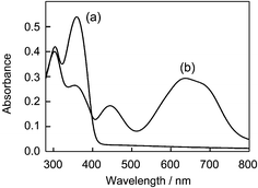 | ||
| Fig. 3 Electronic absorption spectral change of amorphous film of BTPTC. (a) Before photoirradiation. (b) Photostationary state upon irradiation with 365 nm light. | ||
Similar dithienylethene-based photochromic amorphous molecular materials,35,36 dithienylethene-based tetraazaporphyrin37 and phthalocyanine38 have also been reported.
3-2 Application of azobenzene-based photochromic amorphous molecular materials for surface relief grating formation
Formation of surface relief gratings (SRG) observed for azobenzene-functionalised polymers has been a topic of current interest in view of both scientific interest and potential applications for erasable and rewritable holographic memory, polarisation discriminator, and waveguide coupler.39–47 SRG is formed by mass transport induced by the photoisomerisation of the azobenzene chromophore. A few models have been proposed for SRG formation, which include a pressure gradient model,41 an electric-field gradient model,42 and an anisotropic diffusion model.45,46SRG formation using azobenzene-based photochromic amorphous molecular materials was investigated from the viewpoints that azobenzene-based photochromic amorphous molecular materials may also be good candidates for SRG-forming materials and that amorphous molecular materials are suitable for the study of the correlation between molecular structures and SRG-forming properties since they are free from polymer chains and hence their entanglement.32,33
When the amorphous films of azobenzene-based photochromic amorphous molecular materials, e.g., DBAB and BFlAB, were irradiated with two linearly polarised 488 nm Ar+ laser beams (at 10 mW cm−2), SRG formation took place, as confirmed by atomic force microscopy (AFM) (Fig. 4) and by the measurement of diffraction efficiency. The diffraction efficiency, which was monitored by the intensity of the first-order diffraction beam from a He–Ne laser probe beam (633 nm), greatly depended on the polarisation directions of the two writing beams; higher diffraction efficiencies were obtained when the polarised writing beams of either p−/p+ or +45°/−45° with respect to the p-polarisation were irradiated. By contrast, irradiation with writing beams of s-polarisation was not effective for SRG formation. A diffraction efficiency of 23% and a modulation depth of 280 nm as determined by AFM were obtained for BFlAB. The formed SRG was stable, retaining a diffraction efficiency of 80% of the original value even after three months in the dark at room temperature.32 When the sample was heated above its Tg, the SRG disappeared, and a new SRG was again formed by irradiation with the two writing beams at room temperature. These results indicated that the presence of a polymer chain is not necessarily required for the formation of SRG and that photochromic amorphous molecular materials also constitute promising candidates for SRG-forming materials.
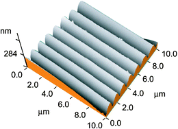 | ||
| Fig. 4 AFM image of SRG formed on amorphous film of BFlAB. | ||
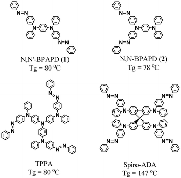
A marked effect of molecular structure on SRG formation was observed for amorphous molecular materials with two azobenzene chromophores, N,N′-bis[4-(phenylazo)phenyl]-N,N′-diphenyl-p-phenylenediamine (N,N′-BPAPD, 1)
(Tg
= 80 °C) and N,N-bis[4-(phenylazo)phenyl]-N,N′-diphenyl-p-phenylenediamine (N,N-BPAPD, 2)
(Tg
= 78 °C).48N,N′-BPAPD was synthesised by the reaction of p-diiodobenzene with 4-(phenylamino)azobenzene. N,N-BPAPD was synthesised by the reaction of 4-aminotriphenylamine with 4-iodoazobenzene. When the amorphous films of 1 and 2 were irradiated with two linearly polarised writing beams, the diffraction efficiency gradually increased with irradiation time and was almost saturated within 5 min. While the diffraction efficiency and the modulation depth of SRG were only 5% and 120 nm for 2, those for 1 were 20% and 240 nm. As it is thought that the ease of molecular motions is similar for 1 and 2 since the Tgs of 1 and 2 are almost the same, the four times greater diffraction efficiency and the doubled modulation depth of SRG observed for 1 relative to 2 are reasonably explained in terms of the anisotropic diffusion model. The model assumes that molecules that absorbed light move to the direction parallel to the long axis of the azobenzene chromophore through the cycles of the photoinduced trans–cis and cis–trans isomerizations of the azobenzene chromophore, escaping from the site where the interference light with a stronger p-polarization component is irradiated to the site where the interference light with a weaker p-polarization component is irradiated.48
SRG formation has also been investigated for other azobenzene-based photochromic amorphous molecular materials, e.g., N,N′-bis(phenyl)-N,N′-bis((4-phenylazo)phenyl)benzidine,49 tris[(4-(phenylazo)diphenylamine)phenylamine] (TPPA),50 and 2,2′,7,7′-tetrakis(4-phenylazodiphenylamino)-9,9′-spirobifluorene (Spiro-ADA).51. It has recently been reported that TPPA having three azobenzene groups formed an SRG with a diffraction efficiency reaching 23% and a modulation depth of 250 nm, and that the crystalline morphology originating from molecular aggregation strongly prevented the SRG formation.50 A high diffraction efficiency of 38% has also been reported for spiro-ADA with high Tg.51
Elucidating differences in SRG-forming properties between amorphous molecular materials and polymers is of great interest. Comparative studies of SRG formation using DBAB and a corresponding vinyl polymer containing the same azobenzene moiety as a pendant group, PVDBAB, showed that SRG was formed more rapidly for the amorphous molecular material than for the corresponding vinyl polymer (Fig. 5).52 It is thought that more facile mass transport in the amorphous molecular material relative to the vinyl polymer is responsible for the faster formation of SRG.
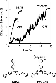 | ||
| Fig. 5 Diffraction efficiency of SRG as a function of irradiation time for amorphous films of DBAB and PVDBAB. | ||
3-3 Application of dithienylethene-based photochromic amorphous molecular materials for image formation and memory
Dithienylethene-based photochromic amorphous molecular materials have found a potential application for dual image formation at the same location.31 Linearly polarised-light induced dichroism was observed for the dithienylethene-based photochromic amorphous molecular materials, and the use of this phenomenon enabled dual image formation at the same location of amorphous film. For example, the amorphous film of the open form of TPTBC was irradiated with non-polarised 365 nm light for 5 min, and then the resulting blue-coloured film was irradiated with polarised red light of horizontal polarisation for 30 s through a mask, where the area other than the letter in the mask is exposed, followed by irradiation with polarised red light of vertical polarisation for another 30 s through another mask, where the area other than the letter in the second mask is exposed. When the film was viewed through a polariser with horizontal polarisation, the letter in the first mask is visible, while the letter in the second mask is visible through a polariser with vertical polarisation. The formation of dual images at the same location can be utilized for seeing a stereo image with glasses using the two polarisers.A nondestructive readout method and a principle of organic bistable molecular memory using photochromic diarylethenes have also been reported.53,54
4 Amorphous molecular resists
Electronic circuit density in semiconductor devices has become increasingly higher year by year, and the minimum feature size required for device fabrication has become smaller. While 1 Gbit DRAMs with a resolution of 130 nm are produced at present, it is expected that 4 Gbit DRAM chips with a resolution of 65 nm will be fabricated in the near future. Both new lithographic processes and new resist materials for future nanolithography are under active investigation. Photolithographic processes have been developed from processes using 436 and 365 nm light from high-pressure mercury lamps to those using 248, 193, and 157 nm light from KrF, ArF, and F2 excimer lasers. Electron-beam lithography, which enables direct writing of nanometer-scale high-resolution patterns without masks, is expected to be a promising candidate for future nanolithographic processes.Polymers and composite polymers have been used as photo- and electron-beam resist materials owing to their capability of uniform amorphous film formation.55 However, a serious problem encountered with polymer resists for the fabrication of nanometer-scale patterns is the fluctuation of line patterns resulting from their large molecular size together with the presence of a molecular-weight distribution, which leads to edge and surface roughness. Reducing the molecular size is an effective approach towards higher resolution in future nanolithography.
Amorphous molecular resists, namely, amorphous molecular materials with resist properties, have advantages over polymer resist materials in their smaller molecular size and the absence of any molecular-weight distribution. Amorphous molecular resists, which form uniform, amorphous films by spin coating from solution, are expected to provide a breakthrough for future nanolithography, enabling the fabrication of nanometer-scale line patterns with a lower degree of edge and surface roughness relative to those fabricated with polymer resists.24
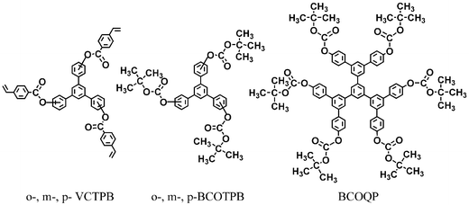
On the basis of this new concept, we have created several novel classes of electron-beam molecular resists.24,56–60 They include 1,3,5-tris[4-(4-toluenesulfonyl)phenyl]benzene (TsOTPB),24 4,4′,4″-tris(allylsuccinimido)triphenylamine (ASITPA),24 1,3,5-tris[(4-vinylphenylcarbonyloxy)phenyl]benzenes (o-, m-, and p-VCTPB),58,59 and a family of chemically amplified, positive-type resists, e.g., 1,3,5-tris(4-tert-butoxycarbonyloxyphenyl)benzene (p-BCOTPB) and 5′,5‴-bis(tert-butoxycarbonyloxy)phenyl-5″-[4,4″-bis(tert-butoxycarbonyloxy)-1,1′ : 3′,1″-terphenyl-5′-yl]-1,1′ : 3′,1″ : 3″,1‴ : 3‴,1‴′-quinquephenyl (BCOQP).56,60 The synthetic route to BCOQP is shown in Scheme 1.
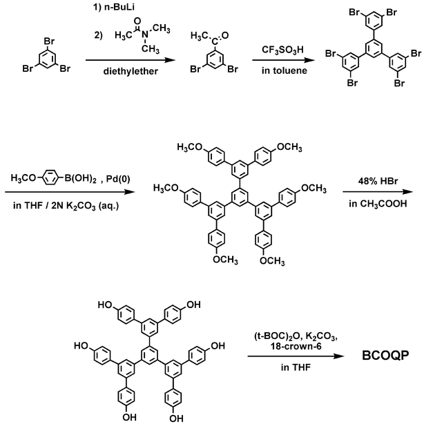 | ||
| Scheme 1 | ||
A positive resist TsOTPB and a negative resist ASITPB permitted the fabrication of 150 and 70 nm line patterns, respectively, on exposure to 50 keV electron beams; however, the sensitivities of these molecular resists were approximately 3 mC cm−2.24 Negative-type electron-beam molecular resists, o-, m-, and p-VCTPB, exhibited much higher sensitivities of ca. 50 µC cm−2 than those for TsOTPB and ASITPA.58,59 A novel class of chemically amplified, positive-type electron-beam molecular resists, o-, m- and p-BCOTPB and BCOQP, have been developed.56,60 Spin-coated films of p-BCOTPB and BCOQP containing 5 wt% diphenyliodonium triflate as an acid generator on a silicon wafer were prebaked for 1–2 min and irradiated with focused electron beams using a scanning electron microscope at 50 keV. The irradiated film was developed with a mixed solvent of tetramethylammonium hydroxide and isopropyl alcohol. The exposed area of the resist film became soluble in the developer solvent because of the transformation of the tert-butoxycarbonyloxy group into the hydroxy group. p-BCOTPB and BCOQP exhibited high sensitivities of 4.4 and 2 µC cm−2, respectively, enabling the fabrication of ca. 40 and 25 nm line patterns, respectively, on exposure to 50 keV electron beams. These sensitivities well meet the requirements of practical use as electron-beam resist materials. Amorphous molecular resists are expected to be promising candidates for future nanolithographic materials.
Related to the amorphous molecular resists described above, vacuum evaporated C60 films have been reported to act as a negative electron-beam resist with a low sensitivity of 10 mC cm−2.61 A nanocomposite resist consisting of subnanometer size C60 and a conventional polymer resist has also been reported.62 Calixarenes have been reported to work as negative electron-beam resists with a sensitivity of 800 µC cm−2.63 No detailed information is available with regard to the morphology of evaporated C60 and calixarenes.
5 Amorphous molecular materials for organic electroluminescent devices
Organic electroluminescent (EL) devices or organic light-emitting diodes (OLEDs) have been the subject of recent extensive studies. They have attracted a great deal of attention in view of both fundamental science and technological applications for full-color, flat-panel displays and lighting.1,64–68 The operation of organic EL devices involves charge injection from electrodes into organic layers, transport of charge carriers, recombination of holes and electrons to generate an electronically excited state or an exciton in the emitting layer, followed by its deactivation by luminescence, either fluorescence or phosphorescence. The main factors that determine luminous and external quantum efficiencies are charge carrier injection from electrodes, charge balance, spin multiplicity of the electronically excited state, emission quantum yield, and light output coupling factor. In order to attain high EL quantum efficiency, it is necessary to achieve efficient charge injection from electrodes at low drive voltage and good charge balance, confining charge carriers within the emitting layer to increase the recombination probability of charge carriers.Usually, layered devices using charge-transporting and charge-blocking layers in addition to the emitting layer have been fabricated in order to meet the above requirements for high performance. The performance of organic EL devices depends upon various materials functioning in specialised roles such as charge-transporting, charge-blocking, and emitting. Both small molecules and polymers have been studied for use as materials in organic EL devices. Amorphous molecular materials that form uniform amorphous thin films by either vacuum deposition or spin coating from solution have proven to be promising materials for organic EL devices. They function as hole-transporting, electron-transporting, hole-blocking, or emitting materials, mainly depending upon their ionisation potentials and electron affinities. Generally, amorphous molecular materials have an advantage over crystalline materials in that the luminescence quantum efficiency in the solid state is not reduced relative to crystalline materials owing to weaker intermolecular π–π interactions.
5-1 Hole-transporting amorphous molecular materials
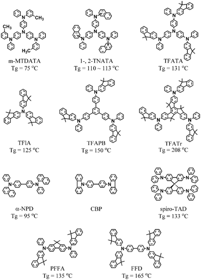
The hole-transport layer in layered organic EL devices plays the roles of facilitating hole injection from the anode into the organic layer and transporting holes, blocking electrons from escaping from the emitting layer to the anode. Therefore, hole-transporting materials should have electron-donating properties to form stable cation radicals and the capability of transporting holes.In order to facilitate hole injection from the ITO electrode into the emitting layer, a hole injection buffer layer has often been inserted between the ITO electrode and the hole-transport layer. The family of TDATA, e.g., 4,4′,4″-tris[3-methylphenyl(phenyl)amino]triphenylamine (m-MTDATA),69,70 4,4′,4″-tris[2-naphthyl(phenyl)amino]triphenylamine (2-TNATA),70 4,4′,4″-tris[biphenylyl(3-methylphenyl)amino]triphenylamine,71 and 4,4′,4″-tris[9,9-dimethylfluoren-2-yl(phenyl)amino]triphenylamine (TFATA),72 have been proven to serve as excellent materials for use in the hole-injection buffer layer. m-MTDATA and its analogues are characterised by very low solid-state ionisation potentials of ca. 5.0 to 5.1 eV, reversible anodic oxidation to give stable cation radicals, and good quality of their amorphous films prepared by vacuum deposition or spin coating from solution. The analysis of current density–voltage characteristics for the hole-only device using m-MTDATA showed that the m-MTDATA/ITO interface is capable of providing trap-free space charge-limited current and that m-MTDATA forms nearly an ohmic contact with the ITO electrode.73–75
N,N′-Bis(3-methylphenyl)-N,N′-diphenyl-[1,1′-biphenyl]-4,4′-diamine (TPD) and N,N′-di(1-naphthyl)-N,N′-diphenyl-[1,1′-biphenyl]-4,4′-diamine (α-NPD) have been widely used as hole transporters in organic EL devices;76,77 however, these materials are not thermally stable. TPD is not morphologically stable either, tending to crystallise readily. A number of hole-transporting amorphous molecular materials with higher Tgs than those of TPD and α-NPD have been developed on the basis of the guideline of the incorporation of rigid moieties, which include TCTA,16 the family of TDAPB, e.g., 1,3,5-tris{4-[methylphenyl(phenyl)amino]phenyl}benzene (o-, m-, and p-MTDAPB)4 and 4,4′,4″-tris[9,9-dimethylfluoren-2-yl(phenyl)aminophenyl]benzene (TFAPB),18 the family of TDAB, e.g., 1,3,5-tris[N-(4-diphenylaminophenyl)phenylamino]benzene,78 the family of TPD, e.g., N,N′-di(biphenyl-4-yl)-N,N′-diphenyl-[1,1′-biphenyl]-4,4′-diamine (p-BPD),79N,N,N′,N′-tetrakis(9,9-dimethylfluorene-2-yl)-[1,1′-biphenyl]-4,4′-diamine (FFD),72 and N,N′-bis(9,9-dimethylfluoren-2-yl)-N,N′-diphenyl-9,9-dimethylfluorene-2,7-diamine (PFFA),80 4,4′-di(N-carbazolyl)biphenyl (CBP),81 2,2′,7,7′-tetrakis(N,N-diphenylamino)-9,9′-spirobifluorene (spiro-TAD),14 tris(9,9-dimethylfluoren-2-yl)amine (TFlA),82 and 2,7,12-tris[9,9-dimethylfluoren-2-yl(phenyl)amino]-5,5,10,10,15,15-hexamethyltruxene (TFATr).20 Most of these materials meet the requirements of reversible anodic oxidation to form stable cation radicals. Materials with ionisation potentials higher than those of materials of the TDATA family are used as the second hole-transporting layer in combination with the first layer which functions as the hole injection buffer layer.
The high-Tg materials enabled the fabrication of high performance, thermally stable, tris(8-quinolinolato)aluminum (Alq3)-based organic EL devices that operate at temperatures above 150 °C.16,72,83 The half-decay time of the 800 cd m−2 initial luminance for a device consisting of 1-TNATA and α-NPD as hole-transport layers, N,N′-diethylquinacridone(QA)-doped Alq3 as an emitting layer, and Alq3 as an electron transport layer was 3200 h at room temperature at constant dc current. The device exhibited high performance with luminous efficiency of 7.5 lm W−1 at 90 °C for obtaining 100 cd m−2 and an external quantum efficiency of 2.2%.84 A truxene-based hole transporter, TFATr, was found to undergo reversible anodic oxidation with almost the same oxidation potential with that of TPD. A device consisting of TFATr and quinacridone-doped Alq3, ITO/TFATr(70 nm)/QA-doped Alq3(40 nm)/Alq3(30 nm)/LiF : Al, exhibited high performance with a turn-on voltage of 2.5 V, a maximum luminance of 86000 cd m−2 at 10.5 V, luminous and external quantum efficiencies of 3.2 lm W−1 and 1.6% at a luminance of 300 cd m−2. The device operated even at 200 °C without any appreciable drop in the initial luminance of 300 cd m−2 (Fig. 6).20
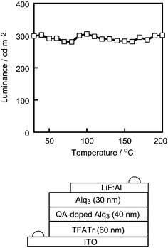 | ||
| Fig. 6 Device structure and temperature dependence of luminance for the device. | ||
The method of the preparation of thin films affects charge injection from electrodes and hence the performance of organic EL devices, depending upon the kinds of materials.85,86 Devices using spin-coated films of TPD or p-BPD as a hole-transport layer and vapor-deposited Alq3 as an emitting layer sandwiched between the ITO and MgAg electrodes exhibited higher injected current density and higher luminance than the corresponding devices using vacuum-deposited films of TPD or p-BPD. On the other hand, no such behaviour was observed for the thin films of m-MTDATA or 2-TNATA.
5-2 Electron-transporting amorphous molecular materials
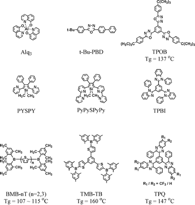
The electron-transport layer plays the roles of facilitating electron injection from the cathode into the organic layer and transporting electrons. It also functions to block holes from escaping from the emitting layer to the cathode. Consequently, electron-transporting materials should have electron-accepting properties to form stable anion radicals and the ability to transport electrons.As compared with various hole-transporting materials, there have been reported fewer electron-transporting materials. Alq3 has been widely used as an excellent electron transporter in organic EL devices. Other reported electron transporters include oxadiazole derivatives, e.g., 2-(biphenyl-4-yl)-5-(4-tert-butylphenyl)-1,3,4-oxadiazole (t-Bu-PBD)76 and 1,3,5-tris(4-tert-butylphenyl-1,3,4-oxadiazoyl)benzene (TPOB),70,87,88 3-(biphenyl-4-yl)-4-phenyl-5-(4-tert-butylphenyl)-1,2,4-triazole (TAZ),89 a benzimidazole derivative (TPBI),90 tris(phenylquinoxaline)
(TPQ),91 silole derivatives, e.g., 1,1-dimethyl-2,5-di(2-pyridyl)silole (PYSPY)92 and 2,5-bis(6′-(2′,2″-bipyridyl))-1,1-dimethyl-3,4-diphenylsilole (PyPySPyPy),93 and boron-containing compounds, e.g., α,ω-bis[bis(dimesitylboryl)]oligothiophenes (BMB-nT)94 and 1,3,5-tris[5-(dimesitylboryl)thiophen-2-yl]benzene (TMB-TB).95 BMB-nT (n
= 1, 2, and 3) and TMB-TB readily form stable amorphous glasses with Tgs above 100 °C and undergo reversible cathodic reduction to form stable anion radicals, exhibiting two or three sequential cathodic and the corresponding anodic waves in their cyclic voltammograms.
BMB-nT with stronger electron-accepting properties than Alq3 were found to serve as an electron injection buffer layers that facilitate electron injection from the Mg cathode into an emitting layer of Alq3 with electron-transporting properties. Multilayer organic EL devices, ITO/m-MTDATA/α-NPD/Alq3/BMB-nT/MgAg, exhibited 10 to 20% higher luminous and quantum efficiencies than the corresponding device without the BMB-nT layer.94
5-3 Hole-blocking amorphous molecular materials
When materials with hole-transporting properties are used as emitters in organic EL devices, the presence of an electron-transport layer with an effective hole-blocking ability is required in order to facilitate electron injection from the cathode into the emitting layer and to block hole carriers to be injected from the emitting layer. However, there have been few electron transporters that function as effective hole blockers at the same time; a well-known electron transporter Alq3 does not necessarily function well as an effective hole blocker; instead, Alq3 itself emits green light as a result of hole injection from the emitting layer. An effective approach for the fabrication of organic EL devices using emitters with hole-transporting properties is the use of a hole-blocking layer inserted between the emitting layer and the electron-transport layer, where the electron-transporting and hole-blocking layers play each role of facilitating electron injection from the cathode and blocking holes from escaping from the emitting layer to confine holes within the emitting layer, respectively.Hole-blocking materials for use in organic EL devices should fulfill several requirements. They should possess proper energy levels of the highest occupied molecular orbital (HOMO) and the lowest unoccupied molecular orbital (LUMO) to be able to block holes from escaping from the emitting layer into the electron-transport layer but to pass on electrons from the electron-transport layer to the emitting layer. In other words, the difference in the HOMO energy levels between the emitting material and the hole-blocking material should be much larger than that in their LUMO energy levels. The materials should have weak electron-accepting properties to form stable anion radicals. In addition, they should not form any exciplexes with emitting materials having electron-donating properties.
Bathocuproine (BCP) has been reported to function as a hole-blocking material;96 however, it forms exciplexes with a number of hole-transporting materials to give new emission at longer wavelength regions.97
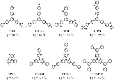
Two families of hole-blocking amorphous molecular materials have been developed. One is a triarylbenzene family,8,98e.g., 1,3,5-tri(biphenyl-4-yl)benzene (TBB), 1,3,5-tris(4-fluorobiphenyl-4′-yl)benzene (F-TBB), 1,3,5-tris(9,9-dimethylfluoren-2-yl)benzene (TFB), and 1,3,5-tris[4-(9,9-dimethylfluoren-2-yl)phenyl]benzene (TFPB). Fluoro-substituted phenylene compounds also serve as hole-blocking materials.99 Another class of hole-blocking amorphous molecular materials are boron-containing compounds,9e.g., tris(2,3,5,6-tetramethylphenyl)borane (TPhB), tris(2,3,5,6-tetramethylbiphenyl-4-yl)borane (TBPhB), tris(2,3,5,6-tetramethyl-1,1′;4′,1″-terphenyl-4-yl)borane (TTPhB), and tris[2,3,5,6-tetramethyl-4-(1,1′;3′,1″-terphenyl-5′-yl)phenyl]borane (TTPhPhB). In addition to the above two families, BMB-2T with a larger ionisation potential than that of Alq3 has also been used as an effective hole-blocking material, as described in the following section.
High performance blue- and blue-violet-emitting organic EL devices have been developed by the use of these hole-blocking materials and TPD, N,N-bis(9,9-dimethylfluoren-2-yl)aniline (F2PA), p-TTA, and α-NPD as blue-violet and blue emitters.8,9,98 For example, a device, ITO/m-MTDATA/TPD/F-TBB/Alq3/MgAg, exhibited blue violet emission with a turn-on voltage of 4.0 V and an external quantum efficiency of 1.40%.8
5-4 Emitting amorphous molecular materials
In any type of devices consisting of a single emitting layer or multilayers with additional charge-transporting and charge-blocking layers, the emitting layer in organic EL devices functions as the recombination center for holes and electrons injected from the anode and cathode, respectively. The generated electronically excited state or the exciton either emits luminescence or serves as a host, transferring its excitation energy to a luminescent dopant. Therefore, materials for use in the emitting layer should accept both hole and electron carriers, that is, the materials should have bipolar character, permitting the formation of both stable cation and anion radicals. The materials should have proper HOMO and LUMO energy levels to be able to accept holes and electrons from adjacent layers without significant energy barriers. The emitting materials should have high luminescence quantum efficiencies. In addition to these requirements, they should be capable of forming smooth, uniform thin films with both thermal and morphological stability. The fulfillment of these requirements is expected to lead to enhanced performance and improved durability of devices.Alq3 has been most widely used as a green emitter or a host material for luminescent dopants. However, its anodic oxidation and cathodic reduction processes are irreversible. The instability of the Alq3 ion radicals might lead to a long-term degradation of Alq3-based organic EL devices.100,101 Some of the reported emitting materials lack information about redox properties, and some materials undergo irreversible oxidation and/or reduction. Ionic transition metal complexes such as ruthenium(II) complexes have bipolar properties,102 but do not tend to form uniform thin films by themselves.
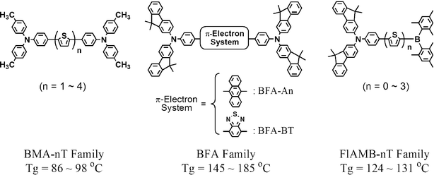
Three novel families of amorphous molecular materials, BMA-nT,10,103–106 BFA-1T,107 BFA-An, BFA-BT,108 and FlAMB-nT,109,110 have provided definite examples of emitting materials that meet all the requirements described above. The incorporation of two bis(4-methylphenyl)aminophenyl groups in the BMA-nT family provided electron-donating properties to accept hole carriers, facilitating amorphous glass formation owing to their nonplanar molecular structures. The central oligothiophene unit provided properties of accepting electrons, controlling emission color depending on the length of π-conjugation. With regard to the BFA family, two bis(4-methylpheny)aminophenyl groups in the BMA-nT family were replaced by two bis(9,9-dimethylfluoren-2-yl)aminophenyl groups in order to increase Tgs. Anthracene, benzothiadiazole, thiophene, and oligothiophene were introduced in the central π-electron system to provide properties of accepting electrons and to control the LUMO energy levels. In the FlAMB-nT family, the incorporation of the bis(dimesitylboryl) group was intended to give electron-accepting properties as well as to facilitate amorphous glass formation. The synthetic route of FlAMB-1T is shown in Scheme 2.
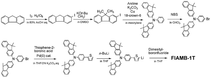 | ||
| Scheme 2 | ||
All the compounds of the above three families were found to readily form stable amorphous glasses with well-defined Tgs, as characterised by DSC, XRD, and IR and Raman spectroscopy.111,112 They exhibited intense fluorescence with relatively high quantum yields. They were found to possess desired bipolar character, undergoing both reversible anodic oxidation and cathodic reduction to permit the formation of stable cation and anion radicals. The HOMO energy levels of BMA-nT (n = 1–4) were almost the same irrespective of the conjugation length of oligothiophene, as determined by cyclic voltammetry and ultraviolet photoelectron spectroscopy.113,114 The π-conjugation length of oligothiophenes mainly affected the LUMO energy levels, tuning the emission colour from blue to green, yellow, and orange. The results of cyclic voltammetry of the FlAMB-nT (n = 0–3) family showed that the oxidation potentials gradually decreased and the reduction potentials became increasingly more positive with increasing conjugation length of the central thiophene unit, leading to the differences of 0.09 and 0.48 V, respectively, between n = 0 and n = 3. The π-conjugation length of the central oligothiophenes finely controlled the HOMO and LUMO energy gap and the emission colour. The HOMO and LUMO energy levels of the BFA family greatly depended on the kinds of the central π-electron system. The materials of the BFA family exhibited intense fluorescence from blue to red, depending upon the kind of the central π-electron system.
These three classes of emitting amorphous molecular materials with desired bipolar properties were found to function as excellent emitting and host materials for emissive dopants for use in organic EL devices. All the fabricated devices consisting of m-MTDATA as a hole-transport layer, BMA-nT, BFA-An, BFA-BT, or FlAMB-nT as an emitting layer, BMB-2T as a hole-blocking layer, and Alq3 as an electron-transport layer sandwiched between the ITO anode and the LiF/Al cathode (Fig. 7) exhibited high performance. Some results are listed in Table 1. The performance of the green-emitting device C in Table 1 was of the highest level among undoped, fluorescence-based green-emitting organic EL devices. FlAMB-nT served as good host materials for emissive dopants, permitting colour tuning and leading to improved performance. For example, the device D using rubrene-doped FlAMB-1T as an emitting layer emitted bright yellow light originating from rubrene, no green emission from FlAMB-1T being observed. White light emission was also obtained by the combination of two emitting materials of FlAMB-nT; a device consisting of m-MTDATA as a hole-transport layer, FlAMB-0T and FlAMB-3T as emitting bilayers, and Alq3 as an electron-transport layer emitted white light with high performance.110
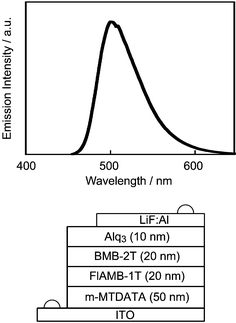 | ||
| Fig. 7 Device structure and electroluminescence spectrum of device C. | ||
| Devicea | Emission colour | Turn on voltageb/V | Maximum luminance/cd m−2 | Luminous efficiencyc/lm W−1 | External quantum efficiencyc (%) |
|---|---|---|---|---|---|
| a A: ITO/TFATA (20 nm)/BFA-An (20 nm)/Alq3 (60 nm)/LiF:Al. B: ITO/m-MTDATA (50 nm)/BFA-BT (20 nm)/BMB-2T (20 nm)/Alq3 (10 nm)/LiF:Al. C: ITO/m-MTDATA (50 nm)/FlAMB-1T (20 nm)/BMB-2T (20 nm)/Alq3 (10 nm)/LiF:Al. D: ITO/m-MTDATA (50 nm)/FlAMB-1T:Rubrene (5 wt%) (20 nm)/BMB-2T (20 nm)/Alq3 (10 nm)/LiF:Al. b Voltage to obtain a luminance of 0.1 cd m−2. c At a luminance of 300 cd m−2. | |||||
| A | Blue | 3.5 | 36900 (at 10.0 V) | 2.0 | 1.3 |
| B | Orange | 2.5 | 23890 (at 10.5 V) | 1.4 | 2.2 |
| C | Green | 2.5 | 26900 (at 12.0 V) | 3.1 | 2.0 |
| D | Yellow | 2.3 | 35740 (at 11.0 V) | 4.3 | 2.1 |
A number of emitting materials are available in the literature,93,115–123 although some of them lack information as to whether they meet the requirements of emitting materials described above. Blue-emitting amorphous molecular materials include BMB-2T,117,118 2,2′-bis(10-phenylanthracen-9-yl)-9,9′-spirobifluorene,119 9-silafluorene-9-spiro-1′-(2′,3′,4′,5′-tetraphenyl)-1′H-silacyclopentadiene,93 spiro-configured terfluorene and others.121 Bis(4-(N-(1-naphthyl)phenylamino)phenyl)fumaronitrile122 and N-methyl-bis(4-(N-(1-naphthyl)-N-phenylamino)phenyl)maleimide123 provide the examples of red-emitting amorphous molecular materials. Organic EL devices using liquid-crystalline materials containing both oxadiazole and amine moieties as emitters or as a matrix have been fabricated and their emission behaviour examined.124,125
The doping of emissive dyes in a host material is as an effective method towards higher performance and enhanced durability of organic EL devices as well as the tuning of emission colour. Rubrene, quinacridone and its derivatives, and DCM dyes are well-known dopants. Recently developed red-emissive dyes that function as dopants include 6,13-diphenylpentacene,126 [7-dimethylamino-3-(2-thienyl)chromen-2-ylidene]-2,2-dicyanovinylamine,127 and {10-(2-thienyl)-2,3,6,7-tetrahydro-1H,5H-chromeno[8,7,6-ij]quinolizin-11-ylidene}-2,2-dicyanovinylamine.127
Phosphorescence-based organic EL devices have recently received a great deal of attention in view of attaining higher quantum efficiency than that of fluorescence-based devices. While the probability of the formation of the electronically excited singlet state as a result of the recombination of holes and electrons is 25%, that of the triplet state is 75%. Triplet phosphors, e.g., iridium,128,129 platinum,130 and europium,131 have been used mostly as dopants dispersed in a host material such as CBP,81 TCTA,16 and F2PA.98 The selection of host materials for triplet phosphors is of crucial importance for attaining efficient energy transfer from the host to the phosphorescent dopant. There is a possibility that the triplet phosphor dopant acts as a recombination center. In this case, the opposite energy transfer from the triplet phosphors to the host material should be prevented.
Amorphous molecular materials are suitable for the investigation of exciplex formation at the organic/organic solid interface because of their homogeneous properties without any grain boundaries. Direct contact between the two layers of the materials of the TDATA family and Alq3 leads to the formation of exciplexes at the interface.132 An organic EL device consisting of the two layers of m-MTDATA and Alq3 emitted yellow light at drive voltages below 8 V and green light at higher drive voltages. While the green emission originates from Alq3, the yellow emission results from the contribution of the exciplex emission.. Thus, the two colours could be reversibly switched, depending upon the drive voltage.132 The exciplex emission can be intensified by the insertion of a thin layer of a mixture of m-MTDATA or 2-TNATA and Alq3 between the two layers.133 Exciplex formation in the organic EL devices has been observed for a number of combinations of hole-transporting and electron-transporting amorphous molecular materials.88,93,134–136 Usually, attention is directed to avoid exciplex formation in organic EL devices. For example, the exciplex formation was prevented by the insertion of a thin layer of a suitable material between the two layers that form an exciplex at the interface.117 On the other hand, the utilisation of intense exciplex emission is one approach for obtaining desired emission colour.135,136
6 Charge transport in the amorphous glassy state and electrically conducting amorphous molecular materials
6-1 Charge transport
Charge transport plays an important role in the operation of photoreceptors in electrophotography, organic EL devices, organic photovoltaic devices, and organic field-effect transistors. It is a subject of great importance to create materials with high charge carrier mobilities for the fabrication of high-performance devices.Charge transport in organic disordered systems has been studied extensively with regard to polymers and molecularly dispersed polymers, where small organic molecules are dispersed in a polymer binder. A few models have been proposed to explain charge transport in disordered systems, which include the Poole–Frenkel model, the small-polaron model, and the disorder formalism. It has been shown that charge transport in molecularly dispersed polymer systems is greatly dependent upon the binder polymer; hole drift mobilities of molecularly dispersed systems vary by two orders of magnitude depending upon the kind of binder polymers.137–139 Creation of amorphous molecular materials has enabled the investigation of charge transport in the amorphous glassy state of small molecules in the absence of any polymer binder.
Recent numerous studies of charge transport in amorphous molecular materials have revealed that the charge-carrier drift mobilities of amorphous molecular materials greatly depend upon molecular structures, being mostly in the range from 10−6 to 10−2 at an electric field of 105 V cm−1 at room temperature, as measured by the time-of-flight method.1,140 The electric-field and temperature dependences of charge carrier drift mobilities have been analysed in terms of the disorder formalism (eqn. (1)), which assumes that charge transport in disordered systems occurs by hopping through a manifold of states, subject to fluctuations in both hopping site energies (energetic disorder) and the intermolecular wavelength overlap (positional disorder)141,142
 | (1) |
The TDATA family71–73 and diarylaminophenylaldehyde arylhydrazones5,143–146 exhibited relatively low mobilities from 10−5 to 10−4 cm2 V−1 s−1. On the other hand, TPD147 and its analogues, e.g., p-BPD79 and FFD,72 TDAPB, and certain triarylamines, e.g., tri(biphenyl-4-yl)amine (TBA),6,148,149p-TTA,140,149 F2PA,149 and TFlA,149 exhibited high mobilities of 10−3 cm2 V−1 s−1 or greater. In particular, thiophene- and selenophene-containing tris(oligoarylenyl)amines, e.g., tris[4-(2-thienyl)phenyl]amine (TTPA), tris[4-(5-phenylthiophen-2-yl)phenyl]amine (TPTPA), tris[4-(2-selenyl)phenyl]amine (TSePA), and tris[4-(5-phenylselenophen-2-yl)phenyl]amine (TPSePA), were found to exhibit very high hole drift mobilities exceeding 10−2 cm2 V−1 s−1 at an electric field of 1.0 × 10⁵ V cm−1 at 293 K in their amorphous glassy states.150 The mobilities exceeding 10−2 are of the highest level among those reported for organic disordered systems. The analysis of the electric-field and temperature dependences of drift mobilities showed that approximately one order of magnitude larger μ0 (1.1–1.8 × 10⁻¹ cm2 V−1 s−1) and relatively small σ (0.063–0.075 eV) are responsible for the high mobilities of TTPA, TPTPA, TSePA, and TPSePA.
On the other hand, reported electron drift mobilities are lower than the hole mobilities, being in the range from 10−6 to 10−4 cm2 V−1 s−1. Tables 2 and 3 list charge carrier drift mobilities of the hole-transporting materials described above and several electron-transporting materials, respectively.
| Material | μ h/cm2 V−1 s−1 | Ref. | Material | μ h/cm2 V−1 s−1 | Ref. |
|---|---|---|---|---|---|
| a Measured at an electric field of ca. 105 V cm−1 at 293 K. | |||||
| m-MTDATA | 3.0 × 10⁻⁵ | 73 | TAPC | 7 × 10⁻³ | 151 |
| p-PMTDATA | 3.0 × 10⁻⁵ | 71 | F2PA | 6.7 × 10⁻³ | 149 |
| 2-TNATA | 5.2 × 10⁻⁵ | 149 | TFlA | 8.1 × 10⁻³ | 149 |
| TFATA | 1.7 × 10⁻⁵ | 72 | p-TTA | 6.9 × 10⁻³ | 140,149 |
| TPD | 1.0 × 10⁻³ | 147 | TTPA | 1.1 × 10⁻² | 150 |
| α-NPD | 8.8 × 10⁻⁴ | 152 | TPTPA | 1.0 × 10⁻² | 150 |
| p-BPD | 1.0 × 10⁻³ | 79 | TSePA | 1.5 × 10⁻² | 150 |
| FFD | 4.1 × 10⁻³ | 72 | TPSePA | 1.1 × 10⁻² | 150 |
The relationship between molecular structure and charge transport properties still remains to be studied. The charge carrier drift mobility has been found to vary greatly depending upon the position of the phenyl group in the biphenyl moiety in the TTA and BPD families. Hole drift mobilities of the o- and p-isomers of TTA and BPD in their glassy states were more than one order of magnitude greater than those of m-TTA and m-BPD.79
6-2 Electrically conducting amorphous molecular materials and their application as materials for organic EL devices
Extensive studies have been performed on organic electrical conductors of small molecules. The previous studies have dealt with only single crystals and polycrystals of charge-transfer complexes, ion-radical salts, and partially oxidised metal complexes. It is of interest to create electrically conducting amorphous molecular materials, which might serve as molecular solders for applications.23 They can also be used as materials for organic photovoltaic devices and organic EL devices. It is expected that increasing the electrical conductivity of materials results in the decrease of bulk resistivity in organic photovoltaic devices and enhances hole injection from the ITO electrode in organic EL devices.Chemical doping of the amorphous films of 4,4′,4″-tris(N-phenothiazinyl)triphenylamine (TPTTA), m-MTDATA, and BMA-nT with iodine has been studied.23,86,158 Doped materials were found to retain the amorphous glassy state without undergoing crystallisation, as evidenced by XRD. The electronic absorption spectra were almost the same as those of anodically oxidised species in solution. The iodine-doped materials were identified as radical cation salts with I3− and I5− as dopants by infrared, Raman, and electronic absorption spectra. The room temperature electrical conductivities of the doped films were in the range from 10−7 to 10−5 S cm−1.
Increasing electrical conductivity of hole-transporting materials would enhance hole injection from the ITO electrode. The use of TDATA and m-MTDATA doped with tetrafluoroquinodimethane (F4TCNQ) in organic EL devices has been reported to enhance hole injection from the ITO electrodes relative to the use of undoped materials, resulting in the reduction of drive voltage.159,160 The effect of iodine doping of m-MTDATA on hole injection currents in a hole-only device, ITO/m-MTDATA/TPD/Ag, and an organic EL device, ITO/m-MTDATA/TPD/Alq3/MgAg, was investigated.158 The current density in the hole-only device using iodine-doped m-MTDATA was approximately two orders of magnitude greater than that of the corresponding device using undoped m-MTDATA at an electric field of 1 × 10⁵ V cm−1. Likewise, an EL device using iodine-doped m-MTDATA as a hole-injection buffer layer exhibited approximately one order of magnitude larger injected current density and higher luminance at an applied voltage of 10 V than the corresponding device using undoped m-MTDATA. The device using iodine-doped m-MTDATA resulted in the reduction of drive voltage relative to the device using undoped m-MTDATA; the turn-on voltages for obtaining a luminance over 1 cd m−2 were 7.7 and 4.5 V, and the drive voltages for obtaining a luminance of 300 cd m−2 were 20.2 and 8.8 V for the devices using undoped and iodine-doped m-MTDATA, respectively. The higher luminance and the doubled external quantum efficiency at the same drive voltage are suggested to result from the increased number of recombined charge carriers and better charge balance in the device using iodine-doped m-MTDATA. Since hole carriers are dominant even in the device using undoped m-MTDATA, the results strongly suggest that not only hole injection from the ITO electrode but also electron injection from the cathode into Alq3 is facilitated when iodine-doped m-MTDATA is used as a hole-injection buffer layer probably because a steeper electric field is applied in the Alq3 layer. Thus, increasing the electrical conductivity of the hole-transport layer is one of the effective methods for enhancing electron injection from the cathode as well as hole injection from the anode, leading to higher performance of organic EL devices.
7 Amorphous molecular materials for organic photovoltaic and photorefractive devices
Organic photovoltaic (PV) devices that directly convert light energy into electrical energy have attracted attention because of their light weight, potentially low cost, and ready fabrication of large-area, thin-film devices. PV devices consist of organic thin films sandwiched between two metal electrodes. The operation processes involve photoabsorption by an organic material to produce an exciton, its diffusion, charge carrier generation by electron transfer, followed by charge separation and charge transport, and charge collection at the electrodes. Significant progress in organic p–n heterojunction devices has been made by the use of copper phthalocyanine and a perylene pigment.161A Schottkey-type device using m-MTDATA sandwiched between the ITO and aluminium electrodes exhibited a conversion efficiency of 0.03%.2 Organic bilayer and trilayer devices using m-MTDATA as an electron donor and Alq3 as an electron acceptor have been fabricated.162 They showed both PV and EL properties. It was found that PV performance was significantly enhanced by the insertion of a thin layer of a mixture of m-MTDATA and Alq3 between the two organic layers of the original m-MTDATA/Alq3 bilayer devices. It is shown that strong exciplex emission in an EL device is a good indicator of efficient charge transfer at the organic interface. m-MTDATA doped with F4TCNQ has been used as a hole-transport layer in bulk heterojunction organic PV devices using zinc phthalocyanine as a donor and C60 as an acceptor.163
Since m-MTDATA responds only to near-UV light, efforts have been made to extend photosensitivity to visible light by the introduction of intramolecular charge transfer. 4,4′,4″-Tris[4-nitrophenyl(4-methylphenyl)amino]triphenylamine (MNTDATA) with a Tg of 134 °C and 4,4′,4″-tris[5-(dimesitylboryl)thiophen-2-yl]triphenylamine (MB-TTPA) with a Tg of 161 °C show electronic absorption bands extending to the wavelength of visible light.164 p–n Heterojunction devices using MNTDATA or MB-TTPA as a p-type semiconductor and anthra[2″,1″,9″:4,5,6:6″5″10″:4′,5′,6′]diisoquino[2,1-a:2′,1′-a′]dibenzimidazole-10,21-dione as an n-type semiconductor responded to visible light, exhibiting conversion efficiencies of 0.4 and 0.1%, respectively, when irradiated with monochromatic light of 440 nm which MNTDATA and MB-TTPA mainly absorb. The BMA-nT series has been modified to show electronic absorption in the visible wavelength region by the replacement of the thiophene unit with a isothianaphthene group.165
A p–n heterojunction photovoltaic device consisting of a triarylphthalocyanine-based amorphous molecular material, PcArA (M: Ti![[double bond, length as m-dash]](https://www.rsc.org/images/entities/char_e001.gif) O), as a p-type semiconductor and N,N′-dimethyl-3,4,9,10-perylenebis(dicarboximide)
(MPCI) as an n-type semiconductor exhibited PV properties when irradiated with 400–600 nm light which MPCI absorbs. The action spectrum resembled the electronic absorption spectrum of MPCI. On the other hand, no photocurrent was observed when the cell was irradiated with 650–900 nm light which PcArA (M: Ti
O), as a p-type semiconductor and N,N′-dimethyl-3,4,9,10-perylenebis(dicarboximide)
(MPCI) as an n-type semiconductor exhibited PV properties when irradiated with 400–600 nm light which MPCI absorbs. The action spectrum resembled the electronic absorption spectrum of MPCI. On the other hand, no photocurrent was observed when the cell was irradiated with 650–900 nm light which PcArA (M: Ti![[double bond, length as m-dash]](https://www.rsc.org/images/entities/char_e001.gif) O) absorbs.166 It is understood that electron transfer takes place from the electronically excited state MPCI to the ground state PcArA to generate electron and hole carriers, whereas the electronically excited PcArA undergoes instant intramolecular charge transfer from the central titanyl phthalocyanine core to the triarylamine unit at the peripheral position instead of electron transfer to MPCI, followed by charge recombination to regenerate the ground state PcArA.
O) absorbs.166 It is understood that electron transfer takes place from the electronically excited state MPCI to the ground state PcArA to generate electron and hole carriers, whereas the electronically excited PcArA undergoes instant intramolecular charge transfer from the central titanyl phthalocyanine core to the triarylamine unit at the peripheral position instead of electron transfer to MPCI, followed by charge recombination to regenerate the ground state PcArA.
It has recently been shown that the use of an additional exciton blocker increases conversion efficiency. BCP has been employed as an exciton blocker in PV cells to improve performance, and a conversion efficiency of ca. 2.5% has been achieved.167
Dye-sensitised, nanocrystalline TiO2 solar cells have recently attracted considerable attention because of their high conversion efficiencies, reaching 10%.168 Hole-transporting amorphous molecular materials have been used in dye-sensitised, nanocrystalline TiO2 solar cells to transport hole carriers from the dye molecule to the counter electrode in place of I3−/I− redox species.169,170
The photorefractive (PR) effect is defined as spatial modulation of the refractive index of materials owing to the formation of space charge upon irradiation with spatially modulated light. It may find potential applications for holographic memories, displays, and optical image amplification.171 The PR effect of organic materials has been reported for amorphous molecular materials,172–175 as well as polymers176–178 and molecularly-doped polymer systems.179,180 Usually, the application of a high external electric field is required for the operation. A poling process is often required to make nonlinear optical materials oriented.
TCTA forms a weak charge-transfer complex with 2,4,7-trinitrofluorenone, exhibiting photoconductivity in response to 633 nm light.181 The material system consisting of a mixture of TCTA as a hole-transporting host material, 2,4,7-trinitrofluorenone as an electron acceptor, and 2,5-dimethyl-4-(p-nitrophenylazo)anisole as a nonlinear optical material exhibited a large PR effect with a two-beam coupling gain coefficient of ca. 100 cm−1 under zero electric field without any poling process.181
Auto-organised amorphous molecular materials with spontaneous nonlinear optical activity without any external poling process have recently been reported.182
Outlook
Organic electronics, optoelectronics, and photonics have attracted increasing attention as a newly emerging field of science and technology that covers chemistry, physics, and materials science. Materials design and synthesis, elucidation of their structures, reactions, and properties, and the fabrication of devices, e.g., organic field effect transistors, PV devices, photorefractive devices, and organic EL devices, have been the major subjects of recent extensive studies. Like crystals and liquid crystalline materials, amorphous molecular materials have also constituted a new class of versatile materials for various applications. Recent numerous studies on amorphous molecular materials have shown a new paradigm of research, paving the way for further developments in the future. There are many challenging subjects remaining to be studied, which include expansion of the scope of amorphous molecular materials to those containing elements other than nitrogen, boron, sulfur, and selenium and to various sorts of complexes other than metal phthalocyanines and metal porphyrins, elucidation of the microstructures of amorphous glasses including short-range ordering and orientation of molecules, correlation between morphologies and reactions and properties, and the search for new applications of amorphous molecular materials.Acknowledgements
The author thanks all the coauthors of the publications cited in this article. The author would also like to thank Dr Z. H. Kafafi of Naval Research Laboratory, Dr M. Ottmar and Professor M. Hanack of Tübingen University, J. T. López Navarrete of University of Malaga, Dr H. Antoniadis of Oslam Co. Ltd, Professor J. Kalinowski of Technical University of Gdańsk, Professor S. T. Lee of City University of Hong Kong, and Professor T. Ikeda of Tokyo Institute of Technology for joint collaboration.References
- Y. Shirota, J. Mater. Chem., 2000, 10, 1 RSC and references cited therein.
- Y. Shirota, T. Kobata and N. Noma, Chem. Lett., 1989, 1145 CAS.
- W. Ishikawa, H. Inada, H. Nakano and Y. Shirota, Chem. Lett., 1991, 1731 CAS; W. Ishikawa, H. Inada, H. Nakano and Y. Shirota, Mol. Cryst. Liq. Cryst., 1992, 211, 431 CAS.
- H. Inada and Y. Shirota, J. Mater. Chem., 1993, 3, 319 RSC.
- K. Nishimura, T. Kobata, H. Inada and Y. Shirota, J. Mater. Chem., 1991, 1, 897 RSC.
- A. Higuchi, K. Ohnishi, S. Nomura, H. Inada and Y. Shirota, J. Mater. Chem., 1992, 2, 1109 RSC.
- D. J. Plazek and J. H. Magill, J. Chem. Phys., 1966, 45, 3038 CrossRef CAS.
- K. Okumoto and Y. Shirota, Appl. Phys. Lett., 2001, 79, 1231 CrossRef CAS.
- M. Kinoshita, H. Kita and Y. Shirota, Adv. Funct. Mater., 2002, 12, 780 CrossRef CAS.
- T. Noda, I. Imae, N. Noma and Y. Shirota, Adv. Mater., 1997, 9, 239 CrossRef CAS.
- S. Yoshikawa, Y. Kotani and Y. Shirota, 69th Annual Meeting of the Chemical Society of Japan, Kyoto, 1995, prepr. no.2, p. 641 Search PubMed; Y. Shirota, K. Moriwaki, S. Yoshikawa, T. Ujike and H. Nakano, J. Mater. Chem., 1998, 8, 2579 Search PubMed.
- M. Ottmar, T. Ichisaka, L. R. Subramanian, M. Hanack and Y. Shirota, Chem. Lett., 2001, 788 CrossRef CAS.
- K. Hirayama, H. Kawai and Y. Shirota, to be submitted for publication.
- J. Salbeck, N. Yu, J. Bauer, F. Weissörtel and H. Bestgen, Synth. Met., 1997, 91, 209 CrossRef CAS.
- S. Wang, W. J. Oldham, Jr., R. A. Hudack, Jr. and G. C. Bazan, J. Am. Chem. Soc., 2000, 122, 5695 CrossRef CAS.
- Y. Kuwabara, H. Ogawa, H. Inada, N. Noma and Y. Shirota, Adv. Mater., 1994, 6, 677 CAS.
- H. Ogawa, H. Inada and Y. Shirota, Macromol. Symp., 1997, 125, 171.
- K. Okumoto, H. Doi and Y. Shirota, J. Photopolym. Sci. Technol., 2002, 15, 239 CAS.
- A. Higuchi, K. Katsuma and Y. Shirota, Koubunshi Ronbunshu, 1996, 53, 829 Search PubMed.
- K. Okumoto and Y. Shirota, 81st Annual Spring Meeting of the Chemical Society of Japan, Tokyo, March 2002, prepr. no. 1, p. 215; 82nd Annual Meeting of the Chemical Society of Japan, Tokyo, March 2003, prepr. no. 1, p. 83; Jpn. Kokai Tokkyo Koho, 2003, 261473 Search PubMed.
- W. Ishikawa, K. Noguchi, Y. Kuwabara and Y. Shirota, Adv. Mater., 1993, 5, 559 CrossRef CAS.
- M. Thelakkat, Macromol. Mater. Eng., 2002, 287, 442 CrossRef CAS.
- A. Higuchi, H. Inada, T. Kobata and Y. Shirota, Adv. Mater., 1991, 3, 549 CrossRef CAS.
- M. Yoshiiwa, H. Kageyama, Y. Shirota, F. Wakaya, K. Gamo and M. Takai, Appl. Phys. Lett., 1996, 69, 2605 CrossRef CAS.
- H. Dürr and H. Bouas-Laurant, Photochromism, Molecules and Systems, Elsevier, Amsterdam, 1990 Search PubMed.
- C. B. McArdle, Applied Photochromic Polymer Systems, Blackie & Son Ltd., New York, 1992 Search PubMed.
- K. Ichimura, Organic Photochromic and Thermochromic Compounds, ed. J. C. Crano and R. J. Guglielmetti, Plenum Press, New York and London, 1999 Search PubMed.
- T. Ujike, K. Moriwaki, H. Nakano and Y. Shirota, J. Photopolym. Sci. Technol., 1998, 11, 33 CAS.
- D. Nagahama, T. Ujike, K. Moriwaki, S. Yoshikawa, H. Nakano and Y. Shirota, J. Photopolym. Sci. Technol., 1999, 12, 277 CAS.
- H. Utsumi, D. Nagahama, H. Nakano and Y. Shirota, J. Mater. Chem., 2000, 10, 2436 RSC.
- H. Utsumi, D. Nagahama, H. Nakano and Y. Shirota, J. Mater. Chem., 2002, 12, 2612 RSC.
- H. Nakano, T. Takahashi, T. Kadota and Y. Shirota, Adv. Mater., 2002, 14, 1157 CrossRef CAS.
- Y. Shirota, H. Utsumi, T. Ujike, S. Yoshikawa, K. Moriwaki, D. Nagahama and H. Nakano, Opt. Mater., 2003, 21, 249 CrossRef CAS.
- T. Tanino, H. Nakano and Y. Shirota, 83rd Annual Meeting of the Chemical Society of Japan, Tokyo, 2003, prepr. No. 1, p. 46.
- M.-S. Kim, T. Kawai and M. Irie, Chem. Lett., 2000, 1188 CAS.
- M. Fukudome, K. Kamiyama, T. Kawai and M. Irie, Chem. Lett., 2001, 70 CrossRef CAS.
- H. Tian, B. Chen, H. Tu and K. Müllen, Adv. Mater., 2002, 14, 918 CrossRef CAS.
- B. Chen, M. Wang, Y. Wu and H. Tian, Chem. Commun., 2002, 1060 RSC.
- P. Rochon, E. Batalla and A. Natansohn, Appl. Phys. Lett., 1995, 66, 136 CrossRef CAS.
- D. Y. Kim, S. K. Tripathy, Lian Li and J. Kumar, Appl. Phys. Lett., 1995, 66, 1166 CrossRef CAS.
- C. J. Barrett, A. L. Natansohn and P. L. Rochon, J. Phys. Chem., 1996, 100, 8836 CrossRef CAS.
- J. Kumar, L. Li, X. Jiang, D.-Y. Kim, T. S. Lee and S. Tripathy, Appl. Phys. Lett., 1998, 72, 2096 CrossRef CAS.
- N. K. Viswanathan, D. Y. Kim, S. Bian, J. Williams, W. Liu, L. Li, L. Samuelson, J. Kumar and S. K. Tripathy, J. Mater. Chem., 1999, 9, 1941 RSC.
- L. Andruzzi, A. Altomare, F. Ciardelli, R. Solaro, S. Hvilsted and P. S. Ramanujam, Macromolecules, 1999, 32, 448 CrossRef.
- P. Lefin, C. Fiorini and J.-M. Nunzi, Pure Appl. Opt., 1998, 7, 71 CrossRef CAS.
- C. Fiorini, N. Prudhomme, G. de Veyrac, I. Maurin, P. Raimond and J.-M. Nunzi, Synth. Met., 2000, 115, 121 CrossRef CAS.
- T. Ubukata, T. Seki and K. Ichimura, Adv. Mater., 2000, 12, 1675 CrossRef CAS.
- H. Ueda, T. Tanino, H. Ando, H. Nakano and Y. Shirota, Chem. Lett., 2004, 33, 1152 CrossRef CAS.
- T. Fuhrmann and T. Tsutsui, Chem. Mater., 1999, 11, 2226 CrossRef CAS.
- M.-J. Kim, E.-M. Seo, D. Vak and D.-Y. Kim, Chem. Mater., 2003, 15, 4021 CrossRef CAS.
- C. Chun, M.-J. Kim, D. Vak and D. Y. Kim, J. Mater. Chem., 2003, 13, 2904 RSC.
- H. Ando, T. Takahashi, H. Nakano and Y. Shirota, Chem. Lett., 2003, 32, 710 CrossRef CAS.
- T. Tsujioka, Y. Hamada, K. Shibata, A. Taniguchi and T. Fuyuki, Appl. Phys. Lett., 2001, 78, 2282 CrossRef CAS.
- T. Tsujioka and H. Kondo, Appl. Phys. Lett., 2003, 83, 937 CrossRef CAS.
- E. Reichmanis, O. Nalamasu and F. M. Houlihan, Macromol. Symp., 2001, 175, 185 CrossRef CAS.
- T. Kadota, H. Kageyama, F. Wakaya, K. Gomo and Y. Shirota, J. Photopolym. Sci. Technol., 1999, 12, 375 CrossRef CAS.
- T. Kadota, H. Kageyama, F. Wakaya, K. Gamo and Y. Shirota, J. Photopolym. Sci. Technol., 2000, 13, 203 CAS.
- T. Kadota, M. Yoshiiwa, H. Kageyama, F. Wakaya, K. Gamo and Y. Shirota, Proc. SPIE-Int. Soc. Opt. Eng., 2001, 4345, 891 Search PubMed.
- T. Kadota, H. Kageyama, F. Wakaya, K. Gamo and Y. Shirota, Mater. Sci. Eng. C, 2001, 16, 91 CrossRef.
- T. Kadota, H. Kageyama, F. Wakaya, K. Gamo and Y. Shirota, Chem. Lett., 2004, 33, 706 CrossRef CAS.
- T. Tada and T. Kanayama, Jpn. J. Appl. Phys., 1996, 35, L63 CrossRef CAS.
- T. Ishii, H. Nozawa and T. Tamamura, J. Photopolym. Sci. Technol., 1997, 10, 651 CAS.
- J. Fujita, Y. Ohnishi, Y. Ochiai and S. Matsui, Appl. Phys. Lett., 1996, 68, 1297 CrossRef CAS.
- C. W. Tang and S. A. VanSlyke, Appl. Phys. Lett., 1987, 51, 913 CrossRef CAS.
- J. H. Burroughes, D. D. C. Bradley, A. R. Brown, R. N. Marks, K. Mackay, R. H. Friend, P. L. Burns and A. B. Holmes, Nature, 1990, 347, 539 CrossRef CAS.
- A. Kraft, A. C. Grimsdale and A. B. Holmes, Angew. Chem., Int. Ed., 1998, 37, 402 CrossRef.
- R. H. Friend, R. W. Gymer, A. B. Holmes, J. H. Burroughes, R. N. Marks, C. Taliani, D. D. C. Bradley, D. A. Dos Santos, J. L. Bredas, M. Logdlund and W. R. Salaneck, Nature, 1999, 397, 121 CrossRef CAS.
- U. Mitshke and P. Bäuerle, J. Mater. Chem., 2000, 10, 1471 RSC.
- Y. Shirota, Y. Kuwabara, H. Inada, T. Wakimoto, H. Nakada, Y. Yonemoto, S. Kawami and K. Imai, Appl. Phys. Lett., 1994, 65, 807 CrossRef CAS.
- Y. Shirota, Y. Kuwabara, D. Okuda, R. Okuda, H. Ogawa, H. Inada, T. Wakimoto, H. Nakada, Y. Yonemoto, S. Kawami and K. Imai, J. Lumin., 1997, 72–74, 985 CrossRef CAS.
- Y. Shirota, K. Okumoto and H. Inada, Synth. Met., 2000, 111–112, 387 CrossRef CAS.
- K. Okumoto and Y. Shirota, Chem. Lett., 2000, 1034 CrossRef CAS.
- C. Giebeler, H. Antoniadis, D. D. C. Bradley and Y. Shirota, Appl. Phys. Lett., 1998, 72, 2448 CrossRef CAS.
- H. Antoniadis, C. Giebeler, D. D. C. Bradley and Y. Shirota, Proc. SPIE-Int. Soc. Opt. Eng., 1998, 3476, 142 Search PubMed.
- C. Giebeler, H. Antoniadis, D. D. C. Bradley and Y. Shirota, J. Appl. Phys., 1999, 85, 608 CrossRef CAS.
- C. Adachi, T. Tsutsui and S. Saito, Appl. Phys. Lett., 1989, 55, 1489 CrossRef CAS.
- S. A. Van Slyke, C. H. Chen and C. W. Tang, Appl. Phys. Lett., 1996, 69, 2160 CrossRef CAS.
- W. Ishikawa, K. Noguchi, Y. Kuwabara and Y. Shirota, Adv. Mater., 1993, 5, 559 CrossRef CAS.
- K. Okumoto, K. Wayaku, T. Noda, H. Kageyama and Y. Shirota, Synth. Met., 2000, 111–112, 473 CrossRef CAS.
- K. Okumoto and Y. Shirota, Mater. Sci. Eng. B, 2001, 85, 135 CrossRef.
- B. E. Koene, D. E. Loy and M. E. Thompson, Chem. Mater., 1998, 10, 2235 CrossRef CAS.
- M. Tanaka, M. Maeda, H. Kageyama and Y. Shirota, to be submitted for publication.
- H. Inada, Y. Yonemoto, T. Wakimoto, K. Imai and Y. Shirota, Mol. Cryst. Liq. Cryst., 1996, 280, 331 CAS.
- H. Murata, C. D. Merrit, H. Inada, Y. Shirota and Z. H. Kafafi, Appl. Phys. Lett., 1999, 75, 3252 CrossRef CAS.
- M. Ishihara, K. Okumoto and Y. Shirota, Chem. Lett., 2003, 32, 162 CrossRef CAS.
- M. Ishihara, K. Okumoto and Y. Shirota, Proc. SPIE-Int. Soc. Opt. Eng., 2004, 5214, 133 Search PubMed.
- J. Bettenhausen and P. Strohriegl, Adv. Mater., 1996, 8, 507 CAS.
- H. Ogawa, R. Okuda and Y. Shirota, Mol. Cryst. Liq. Cryst., 1998, 315, 187.
- J. Kido, C. Ohtaki, K. Hongawa, K. Okuyama and K. Nagai, Jpn. J. Appl. Phys., 1993, 32, L917 CAS.
- Z. Gao, C. S. Lee, I. Bello, S. T. Lee, R.-M. Chen, T.-Y. Luh, J. Shi and C. W. Tang, Appl. Phys. Lett., 1999, 74, 865 CrossRef CAS.
- M. Jandke, P. Strohriegl, S. Berleb, E. Werner and W. Brütting, Macromolecules, 1998, 31, 6434 CrossRef CAS.
- K. Tamao, M. Uchida, T. Izumizawa, K. Furukawa and S. Yamaguchi, J. Am. Chem. Soc., 1996, 118, 11974 CrossRef CAS.
- L. C. Palilis, H. Murata, M. Uchida and Z. H. Kafafi, Org. Electron., 2003, 4, 113 Search PubMed.
- T. Noda and Y. Shirota, J. Am. Chem. Soc., 1998, 120, 9714 CrossRef CAS.
- M. Kinoshita and Y. Shirota, Chem. Lett., 2001, 614 CrossRef CAS.
- Y. Kijima, N. Asai and S. Tamura, Jpn. J. Appl. Phys., 1999, 38, 5274 CrossRef CAS.
- Y. Shirota, M. Kinoshita and K. Okumoto, Proc. SPIE-Int. Soc. Opt. Eng., 2002, 4464, 203 Search PubMed.
- K. Okumoto and Y. Shirota, Chem. Mater., 2003, 15, 699 CrossRef CAS.
- M. Ikai, S. Tokito, Y. Sakamoto, T. Suzuki and Y. Taga, Appl. Phys. Lett., 2001, 79, 156 CrossRef CAS.
- H. Aziz, Z. D. Popovic, N.-X. Hu, A. M. Hor and G. Xu, Science, 1999, 283, 1900 CrossRef CAS.
- Z. D. Popovic, H. Aziz, N.-X. Hu, A. M. Hor and G. Xu, Synth. Met., 2000, 111–112, 229 CrossRef CAS.
- H. Rudmann and M. F. Rubner, J. Appl. Phys., 2001, 90, 4338 CrossRef CAS.
- T. Noda, H. Ogawa, N. Noma and Y. Shirota, Appl. Phys. Lett., 1997, 70, 699 CrossRef CAS.
- T. Noda, H. Ogawa, N. Noma and Y. Shirota, Adv. Mater., 1997, 9, 720 CrossRef CAS.
- T. Noda, H. Ogawa, N. Noma and Y. Shirota, J. Mater. Chem., 1999, 9, 2177 RSC.
- Y. Ohsedo, T. Yamate, K. Okumoto and Y. Shirota, J. Photopolym. Sci. Technol., 2001, 14, 297 CAS.
- K. Okumoto, T. Ohara, T. Noda and Y. Shirota, Synth. Met., 2001, 121, 1655 CrossRef CAS.
- M. Maeda, K. Hashimoto, K. Okumoto and Y. Shirota, Polym. Prepr. Jpn., 2004, 53(2), 4559 Search PubMed.
- Y. Shirota, M. Kinoshita, T. Noda, K. Okumoto and T. Ohara, J. Am. Chem. Soc., 2000, 122, 11021 CrossRef CAS.
- H. Doi, M. Kinoshita, K. Okumoto and Y. Shirota, Chem. Mater., 2003, 15, 1080 CrossRef CAS.
- C. Moreno Castro, M. C. Ruiz Delgado, V. Hernandez, Y. Shirota and J. T. Lopez Navarrete, J. Phys. Chem. B, 2002, 106, 7163 CrossRef.
- J. Casado, M. C. Ruiz Delgado, Y. Shirota, V. Hernandez and J. T. Lopez Navarrete, J. Phys. Chem. B, 2003, 107, 2637 CrossRef CAS.
- A. J. Mäkinen, I. G. Hill, T. Noda, Y. Shirota and Z. H. Kafafi, Appl. Phys. Lett., 2001, 78, 670 CrossRef CAS.
- A. J. Mäkinen, I. G. Hill, M. Kinoshita, T. Noda, Y. Shirota and Z. H. Kafafi, J. Appl. Phys., 2002, 91, 5456 CrossRef CAS.
- H. Ogawa, K. Ohnishi and Y. Shirota, Synth. Met., 1997, 91, 243 CrossRef CAS.
- N. Tamoto, C. Adachi and K. Nagai, Chem. Mater., 1997, 9, 1077 CrossRef CAS.
- T. Noda, H. Ogawa and Y. Shirota, Adv. Mater., 1999, 11, 283 CrossRef CAS.
- T. Noda and Y. Shirota, J. Lumin., 2000, 87–89, 1168 CrossRef CAS.
- W.-J. Shen, R. Doda, C.-C. Wu, F.-I. Wu, T.-H. Liu, H.-H. Chen, C. H. Chen and C.-F. Shu, Chem. Mater., 2004, 16, 930 CrossRef.
- Y. Geng, D. Katsis, S. W. Culligan, J. J. Qu, S. H. Chen and L. J. Rothenberg, Chem. Mater., 2002, 14, 463 CrossRef CAS.
- H. Benmansour, T. Shioya, Y. Sato and G. C. Bazan, Adv. Funct. Mater., 2003, 13, 883 CrossRef CAS.
- H.-C. Yeh, S.-J. Yeh and C.-T. Chen, Chem. Commun., 2003, 2632 RSC.
- H.-C. Yeh, L.-H. Chan, W.-C. Wu and C.-T. Chen, J. Mater. Chem., 2004, 14, 1293 RSC.
- H. Mochizuki, T. Hasui, T. Shiono, T. Ikeda, C. Adachi, Y. Taniguchi and Y. Shirota, Appl. Phys. Lett., 2000, 77, 1587 CrossRef CAS.
- H. Mochizuki, T. Hasui, M. Kawamoto, T. Shiono, T. Ikeda, C. Adachi, Y. Taniguchi and Y. Shirota, Chem. Commun., 2000, 1923 RSC.
- L. C. Picciolo, H. Murata and Z. H. Kafafi, Appl. Phys. Lett., 2001, 78, 2378 CrossRef CAS.
- J. Yu and Y. Shirota, Chem. Lett., 2002, 984 CrossRef CAS.
- M. A. Baldo, S. Lamansky, P. E. Thompson and S. R. Forrest, Appl. Phys. Lett., 1999, 75, 4 CrossRef CAS.
- S. Lamansky, P. Djurovich, D. Murphy, F. Abdel-Razzaq, H.-E. Lee, C. Adachi, P. E. Burrows, S. R. Forrest and M. E. Thompson, J. Am. Chem. Soc., 2001, 123, 4304 CrossRef CAS.
- M. A. Baldo, D. F. O'Brien, Y. You, A. Shoustikov, S. Sibley, M. E. Thompson and S. R. Forrest, Nature, 1998, 395, 151 CrossRef CAS.
- J. Fang and D. Ma, Appl. Phys. Lett., 2003, 83, 4041 CrossRef CAS.
- K. Itano, H. Ogawa and Y. Shirota, Appl. Phys. Lett., 1998, 72, 636 CrossRef CAS.
- K. Okumoto and Y. Shirota, J. Lumin., 2000, 87–89, 1171 CrossRef CAS.
- H. Ogawa, R. Okuda and Y. Shirota, Appl. Phys. A, 1998, 67, 599 CrossRef.
- M. Cocchi, D. Virgili, G. Giro, V. Fattori, P. Di Marco, J. Kalinowski and Y. Shirota, Appl. Phys. Lett., 2002, 80, 2401 CrossRef CAS.
- M. Guan, Z. Q. Bian, Y. F. Zhou, F. Y. Li, Z. J. Li and C. H. Huang, Chem. Commun., 2003, 2708 RSC.
- T. Sasakawa, T. Ikeda and S. Tazuke, J. Appl. Phys., 1989, 65, 2750 CrossRef CAS.
- P. M. Borsenberger, J. Appl. Phys., 1990, 68, 5188 CrossRef CAS.
- H.-J. Yuh and D. M. Pai, Mol. Cryst. Liq. Cryst., 1990, 183, 217 CAS.
- Y. Shirota, S. Nomura and H. Kageyama, Proc. SPIE-Int. Soc. Opt. Eng., 1998, 3476, 132 Search PubMed and references cited therein.
- H. Bässler, Phys. Status Solidi B, 1981, 107, 9.
- H. Bässler, Phys. Status Solidi B, 1993, 175, 15 CrossRef.
- K. Nishimura, H. Inada, T. Kobata, Y. Matsui and Y. Shirota, Mol. Cryst. Liq. Cryst., 1992, 217, 235 CAS.
- S. Nomura, K. Nishimura and Y. Shirota, Mol. Cryst. Liq. Cryst., 1994, 253, 79.
- S. Nomura, K. Nishimura and Y. Shirota, Thin Solid Films, 1996, 273, 27 CrossRef CAS.
- S. Nomura and Y. Shirota, Chem. Phys. Lett., 1997, 268, 461 CrossRef CAS.
- M. Stolka, J. F. Yanus and D. M. Pai, J. Phys. Chem., 1984, 88, 4707 CrossRef CAS.
- H. Inada, K. Ohnishi, S. Nomura, A. Higuchi, H. Nakano and Y. Shirota, J. Mater. Chem., 1994, 4, 171 RSC.
- M. Tanaka, K. Okumoto, A. Mozer, H. Kageyama and Y. Shirota, to be submitted for publication.
- H. Ohishi, M. Tanaka, H. Kageyama and Y. Shirota, Chem. Lett., 2004, 33, 1266 CrossRef CAS.
- P. M. Borsenberger, L. Pautmeier, R. Richert and H. Bässler, J. Chem. Phys., 1991, 94, 8276 CrossRef CAS.
- Z. Deng, S. T. Lee, D. P. Webb, Y. C. Chan and W. A. Gambling, Synth. Met., 1999, 107, 107 CrossRef CAS.
- R. G. Kepler, P. M. Beeson, S. J. Jacobs, R. A. Anderson, M. B. Sinclair, V. S. Valencia and P. A. Cahill, Appl. Phys. Lett., 1995, 66, 3618 CrossRef CAS.
- G. G. Malliaras, Y. Shen, D. H. Dunlap, H. Murata and Z. H. Kafafi, Appl. Phys. Lett., 2001, 79, 2582 CrossRef CAS.
- H. Murata, G. G. Malliaras, M. Uchida, Y. Shen and Z. H. Kafafi, Chem. Phys. Lett., 2001, 339, 161 CrossRef CAS.
- M. Redecker, D. D. C. Bradley, M. Jandke and P. Strohriegl, Appl. Phys. Lett., 1999, 75, 109 CrossRef CAS.
- T. C. Wong, J. Kovac, C. S. Lee, L. S. Hung and S. T. Lee, Chem. Phys. Lett., 2001, 334, 61 CrossRef CAS.
- M. Ishihara, T. Noda, H. Kageyama, H. Nakano and Y. Shirota, Synth. Met., 2001, 120, 795 CrossRef CAS.
- X. Zhou, M. Pfeiffer, J. Blochwitz, A. Werner, A. Nollau, T. Fritz and K. Leo, Appl. Phys. Lett., 2001, 78, 410 CrossRef CAS.
- X. Zhou, J. Blochwitz, M. Pfeiffer, A. Nollau, T. Fritz and K. Leo, Adv. Funct. Mater., 2001, 11, 310 CrossRef CAS.
- C. W. Tang, Appl. Phys. Lett., 1986, 48, 183 CrossRef CAS.
- Z. R. Hong, C. S. Lee, S. T. Lee, W. L. Li and Y. Shirota, Appl. Phys. Lett., 2002, 81, 2878 CrossRef CAS.
- D. Gebeyehu, B. Maennig, J. Drechsel, K. Leo and M. Pfeiffer, Solar Energy Mater. Solar Cells, 2003, 79, 81 CrossRef CAS.
- M. Kinoshita, N. Fujii, T. Tsuzuki and Y. Shirota, Synth. Met., 2001, 121, 1571 CrossRef CAS.
- R. Kisselev and M. Thelakkat, Chem. Commun., 2002, 1530 RSC.
- T. Ichisaka, M. Ottmar, H. Kageyama, Y. Shirota, M. Fujitsuka, O. Ito, L. R. Subramanian and M. Hanack, presented at Second International Conference on Porphyrins and Phthalocyanines, Kyoto, Japan, June 30–July 5, 2002, to be submitted for publication.
- P. Peumans, V. Bulovic and S. R. Forrest, Appl. Phys. Lett., 2000, 76, 2650 CrossRef CAS.
- M. K. Nazeeruddin, A. Kay, I. Rodicio, R. Humphry-Baker, E. Muller, P. Liska, N. Vlachopoulos and M. Grätzel, J. Am. Chem. Soc., 1993, 115, 6382 CrossRef CAS.
- J. Hagen, W. Schaffrath, P. Otschik, R. Fink, A. Bacher, H.-W. Schmidt and D. Haarer, Synth. Met., 1997, 89, 215 CrossRef CAS.
- U. Bach, D. Lupo, P. Comte, J. E. Moser, F. Ewissortel, J. Salbeck, H. Spreitzer and M. Grätzel, Nature, 1998, 395, 583 CrossRef.
- W. E. Moerner and S. M. Silence, Chem. Rev., 1994, 94, 127 CrossRef CAS.
- P. M. Lundquist, R. Wortmann, C. Geletneky, R. J. Twieg, M. Jurich, V. Y. Lee, C. R. Moylan and D. M. Burland, Science, 1996, 274, 1182 CrossRef CAS.
- L. Wang, Y. Zhang, T. Wada and H. Sasabe, Appl. Phys. Lett., 1996, 69, 728 CrossRef CAS.
- C. Hohle, U. Hofmann, S. Schloter, M. Thelakkat, P. Strohriegl, D. Haarer and S. J. Zilker, J. Mater. Chem., 1999, 9, 2205 RSC.
- F. Wurthner, R. Wortmann and K. Meerholz, ChemPhysChem, 2002, 3, 17 CrossRef CAS.
- S. Ducharme, J. C. Scott, R. J. Twieg and W. E. Moerner, Phys. Rev. Lett., 1991, 66, 1846 CrossRef CAS.
- B. Kippelen, K. Tamura, N. Peyghambarian, A. B. Padias and H. K. Hall, Jr., Phys. Rev. B, 1993, 48, 10710 CrossRef.
- Z. Peng, A. R. Gharavi and L. Yu, Appl. Phys. Lett., 1996, 69, 4002 CrossRef CAS.
- K. Meerholz, B. L. Volodin, Sandalphon, B. Kippelen and N. Peyghambarian, Nature, 1994, 371, 497 CrossRef CAS.
- D. Wright, U. Gubler, Y. Roh, W. E. Moerner, M. He and R. J. Twieg, Appl. Phys. Lett., 2001, 79, 4274 CrossRef CAS.
- H. Kageyama, N. Kamiyoshi, T. Okamoto and Y. Shirota, to be submitted for publication.
- E. Ishow, C. Bellaïche, L. Bouteiller, K. Nakatani and J. A. Delaire, J. Am. Chem. Soc., 2003, 125, 15744 CrossRef CAS.
| This journal is © The Royal Society of Chemistry 2005 |

