UV-assisted capillary force lithography for engineering biomimetic multiscale hierarchical structures: From lotus leaf to gecko foot hairs
Hoon Eui
Jeong
a,
Rhokyun
Kwak
a,
Ali
Khademhosseini
bc and
Kahp Y.
Suh
*ad
aSchool of Mechanical and Aerospace Engineering, Seoul National University, Seoul 151-742, Korea. E-mail: sky4u@snu.ac.kr
bCenter for Biomedical Engineering, Department of Medicine, Brigham and Women's Hospital, Harvard Medical School, Boston, MA 021158, USA
cHarvard-MIT Division of Health Sciences and Technology, Massachusetts Institute of Technology, Cambridge, MA 02139, USA
dWorld Class University Program on Multiscale Mechanical Design, Seoul National University, Seoul 151-742, Korea
First published on 1st October 2009
Abstract
This feature article provides an overview of the recently developed two-step UV-assisted capillary force lithography and its application to fabricating well-defined micro/nanoscale hierarchical structures. This method utilizes an oxygen inhibition effect in the course of UV irradiation curing and a two-step moulding process, to form multiscale hierarchical or suspended nanobridge structures in a rapid and reproducible manner. After a brief description of the fabrication principles, several examples of the two-step UV-assisted moulding technique are presented. In addition, emerging applications of the multiscale hierarchical structures are briefly described.
1. Introduction
Recently much attention has been paid to the fabrication of various hierarchical structures that contain both micro- and nanoscale features. Multiscale, hierarchical structures are of potential benefit for the development of various biomimetic ,1–5 biomedical,6–8 micro/nanofluidic,9–12 photonic13–16 and electronic17–19 devices since such structures can enhance structural functionality, device performance and even lead to distinct properties compared to those of individual lengthscale structures.1–19 Therefore, much research has been performed to engineer multiscale hierarchical structures based on various bottom-up and top-down approaches. These hierarchical structures can be classified based on their structural features, material properties and desired applications (see Fig. 1).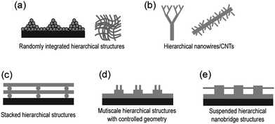 | ||
| Fig. 1 Schematic illustration of the various categories of multiscale hierarchical structures. | ||
In general, randomly integrated or branched hierarchical structures, which correspond to Fig 1a–b, have been generated by bottom-up approaches such as silicon etching,3self-assembly,20 micelle aggregation,21 phase separation22 and growth of carbon nanotubes and nanowires.18,23–25 One of the major advantages of such bottom-up methods is that it provides a facile and efficient route to generating multiscale hierarchical structures. Moreover, nanostructures, with feature sizes that are as small as a few tens of nanometres, can be obtained in a hierarchical format without the use of expensive and sophisticated processes. These approaches are especially useful for the fabrication of superhydrophobic surfaces3–5 or biomimetic scaffolds for tissue engineering.6 However, a limitation of this approach is that the self-organization is often limited by the range of design specification and lacks precise control over geometrical parameters, often generating randomly oriented or fractal-like hierarchical structures (Fig 1a–b).
In contrast, well-defined multiscale hierarchical structures, which correspond to Fig. 1c–e, have been fabricated by top-down approaches. Top-down approaches are based on unconventional lithographic techniques such as reversal imprinting,26,27 transfer printing28,29 and multi-step moulding.5,30,31 As compared to the bottom-up methods, these techniques offer more control in fabricating well-defined hierarchical structures in a predetermined manner. However, despite these advantages, there are a number of limitations with these approaches that have prevented their widespread use. For example, previous multi-step moulding techniques have utilized thermoplastic polymers such as polystyrene (PS) or polymethyl methacrylate (PMMA). In these instances, a high-resolution nanopatterned mould is pressed on preformed polymer microstructures that have been heated to above the polymer glass transition temperature (Tg) to generate combined micro/nanoscale hierarchical structures. Thus, the underlying microstructures are prone to collapse above Tg in the presence of a small loading pressure or other external stimulus.5 Therefore, high-aspect-ratio hierarchical structures are difficult to fabricate with these methods. Moreover, pattern uniformity over a larger area would be diminished. While transfer printing and reversal imprint methods are useful for generating 3D structures by stacking individual structured layers in a serial manner, the fabrication of hierarchical structures with complex geometry and high aspect ratio has not been demonstrated with these methods.26–29
In this feature article, we aim to provide an overview of the recently developed two-step UV-assisted capillary force lithography (CFL) method for generating robust multiscale, hierarchical structures with controllable geometry by overcoming several shortcomings of the previous methods. By exploiting the two-step UV-assisted CFL technique, one can fabricate complex hierarchical structures or suspended nanobridge structures in a geometrically-controllable manner.2,32,33 This review is comprised of three major parts. In the first part, fabrication principles of the two-step UV-assisted CFL are described. In the second part, several examples of the technique are described. Finally, emerging applications of the multiscale hierarchical structures are briefly discussed with emphasis on the fabrication of structures that mimic the lotus leaf and the gecko feet.
2. Two-step UV-assisted capillary force lithography (CFL)
2.1 Principles of two-step UV-assisted CFL
The two-step UV-assisted CFL exploits the inhibition effects of oxygen during photo-polymerization. Oxygen inhibition during the UV curing process is a process in which oxygen inhibits free radical polymerization by reacting with initiator radicals. This process has often been considered as a negative factor in thin film coating processes since it results in low rates of polymerization , under-curing, tacky surfaces and loss of desired optical properties.34–36 In the two-step UV-assisted CFL process, this seemingly undesirable effect has been utilized as a positive element to construct multiscale structures. A key finding is that a partially cured microstructure can be further moulded by sequential application of a nanopatterned mould, resulting in a monolithic hierarchical structure.32By utilizing UV curing kinetics, the UV-assisted CFL technique has several advantages. First, nanostructures can be precisely formed without any collapse or deformation of the preformed microstructures, which has been a major drawback of the multi-step moulding methods using thermoplastic resins.32,33 This is because only the top surface of the resin in contact with oxygen partially cures whereas the resin beneath the surface cures completely (see Fig. 2). During the moulding process, trapped air remains inside the mould cavity. Moreover, atmospheric air permeates through a porous mould (e.g., polydimethylsiloxane, PDMS). Thus, the surface of the moulded resin is directly exposed to air. As a result, UV curing of the resin surface is significantly hindered by the trapped or permeated oxygen that reacts with the radicals generated from the photoinitiator, resulting in a partially cured, tacky surface. In contrast, even though there is a small amount of pre-dissolved oxygen inside the liquid precursor, it is rapidly consumed during the UV curing process due to high mobility and reactivity of oxygen with a large amount of initial radicals. As the diffusivity of oxygen in the UV curable resin is relatively low (e.g. oxygen diffusivity DPUA = 10−13–10−12 m2 s−1),37 oxygen may not penetrate deeply into the polymer layer. Therefore, the inside of the resin would be cured completely as opposed to the top surface. As a result, a variety of nanostructures could be formed on the partially cured microstructures, thus enabling the generation of complex hierarchical structures with tunable geometry and aspect ratio.2,32,38 In addition, monolithic bridges can also be formed by placing a polyurethane acrylate (PUA) mould having engraved nanochannels on a base microstructure under low vacuum conditions (∼10−2 Pa).33 In small-scale channels or pores, capillary force is dominant and usually directs fluid flow along the walls. For a partially cured polymer that is less fluidic, the capillary force is not sufficiently high to guide migration over a long channel spanning the underlying base structures. As a result, at atmospheric pressure, nanostructures are only formed over the underlying microstructures by the fabrication method presented here. When the pressure is reduced to low level vacuum (∼10−2 Pa), however, even a partially cured layer can move into a long channel, thereby forming a suspended bridge structure after complete curing and mould removal.
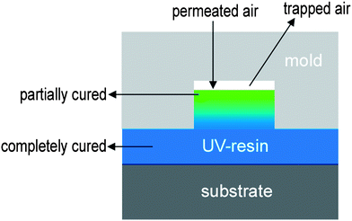 | ||
| Fig. 2 Schematic illustration of the UV light-induced partial curing induced by the trapped or permeated air. | ||
The second advantage is a short process time. As the room-temperature UV irradiation curing induces rapid curing of a solvent-free liquid resin into a solid polymeric structure within a few tens of seconds, the overall process time can be significantly reduced (<3 min).39 Large-area uniformity is another advantage of the current fabrication technique. While thermoplastic-based methods lack the desired uniformity in the resulting structures (due to collapse of the underlying microstructures, high viscosity, air trap and contact failure at the mould/polymer or the polymer/substrate interface), well defined hierarchical structures can be achieved over a large area with high uniformity (>5 × 5 cm2) by optimizing the UV-assisted moulding method.5
2.2 Fabrication results of two-step UV-assisted CFL
Fig. 3 shows a schematic diagram of the two-step UV-assisted CFL process. In the first moulding step, a UV-curable polymer resin of PUA was drop-dispensed on a solid substrate and subsequently partially cured by exposure to UV light (<30 s) (λ = 250–400 nm, intensity = 100 mW cm−2). With this curing time, the top layer was only cured partially, rendering the surface tacky and partially fluidic (1stmoulding). As previously explained, this is because the trapped or permeated air inside the mould inhibits radical polymerization of the PUA resin.35,39 Nanofabrication on the fabricated microstructures (2ndmoulding) was subsequently carried out by applying a nanoscale PUA mould with a low pressure (∼103 Pa) followed by an additional UV exposure for 10 s. The PUA mould has been recently introduced for sub-100-nm patterning. While PDMS is not suitable for sub-100 nm patterning due to low elastic modulus (∼1.8 MPa), the PUA mould is not only sufficiently rigid (Young's modulus of 19.8–320 MPa) but also flexible (∼50 µm thickness), enabling its use for nanopatterning over a large area.40,41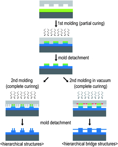 | ||
| Fig. 3 Schematic illustration of the fabrication of the micro/nanoscale combined hierarchical structures by using the two-step UV-assisted capillary force lithography (CFL). Polymer microstructures were formed by using a micropatterned mould followed by fabrication of nanostructures on top of the preformed microstructures by using a nanopatterned PUA mould. Under vacuum conditions, monolithic, suspended bridge structures can be fabricated. | ||
Fig. 4 shows representative scanning electron microscopy (SEM) images of engineered hierarchical structures on a PET (∼50 µm thickness) substrate. As it can be seen, nanopillars that are 100 nm diameter were integrated with the underlying microstructures without deformation of the base microstructure. Also, the integration of various nanostructures such as lines, holes and complex circuit patterns on the 50 nm scale, whether positive (features sticking out) or negative (features sticking in), was also demonstrated using the same approach.32,38 It is noteworthy that either silicon or glass can be used as the substrate instead of the flexible PET.
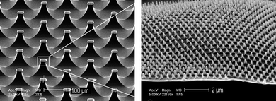 | ||
| Fig. 4 SEM images showing 100 nm pillars formed on 30 µm posts (spacing of 40 µm, height of 50 µm). Reproduced from ref. 32. | ||
In addition to the hierarchical structures described so far, simple monolithic bridge structures can be obtained by carrying out the UV-assisted CFL process at low vacuum (≈10−2 Pa) after placing a PUA mould having nanoscale lines or meshes on top of the partially cured base microstructure. In this process, air pressure was rapidly reduced to 10−2 Pa in a vacuum chamber while the nanopatterned mould was in place. In the course of reaching a low-level vacuum, the partially cured upper layer started to fill into the channel of the nanoscale mould by an omni-directional hydraulic pressure gradient, resulting in the formation of a suspended bridge structure as shown in Fig. 5.33 During the formation of a bridge structure, polymer mass is continuously supplied from the partially cured resin on the top layer. By using this process, complex features (e.g., meshes, concentric circles) could be fabricated on various underlying microstructures with high pattern fidelity. In this method, it is crucial to control the UV exposure time for partial curing of the base microstructures. If the curing time is too short, the microstructures collapse in the presence of a small mechanical loading during the second moulding process. Alternatively, if the time is too long, the nanostructures can not be formed on the completely cured microstructure due to non-fluidity of the UV-curable resin. However, by using an optimal curing time, the upper part of the microstructure will remain fluidic (tacky), allowing for subsequent formation of nanostructures over the preformed microstructures.
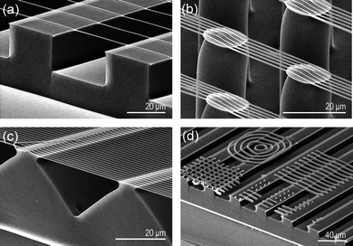 | ||
| Fig. 5 Tilted cross-sectional SEM images for various monolithic nanowire bridge structures of (a–c) nanolines and (d) meshes and concentric circles formed over each underlying microstructure. | ||
It is worthwhile noting that these multiscale hierarchical structures are difficult to fabricate by other methods due to technical or economical limitations. For example, photolithography requires a two-step process with application of a microscale mask followed by a nanoscale mask, which is not cost-effective and would suffer from swelling or deformation of the preformed microstructure. Although electron-beam lithography can serve as a tool for high-resolution nanopatterning, it is too slow and costly. Moreover, previous moulding methods that involved thermoplastic polymers often resulted in deformation or collapse of the preformed microstructures. Also, high-aspect-ratio nanopillars are not fabricated by transfer-based approaches. As compared to these techniques, the two-step UV-assisted CFL presented here offers a robust and highly efficient route to fabricating multiscale, hierarchical structures.
2.3 Theoretical analysis of two-step UV-assisted CFL
In the two-step UV-assisted CFL technique, the inhibitory effect of oxygen on the UV radiation polymerization is a key parameter. Thus, analysis of oxygen concentration with time and space is essential to fully understand the fabrication mechanism. To this end, we consider a one-dimensional governing equation for oxygen inside the cavity of the micromould (see Fig. 6a), which is given by | (1) |
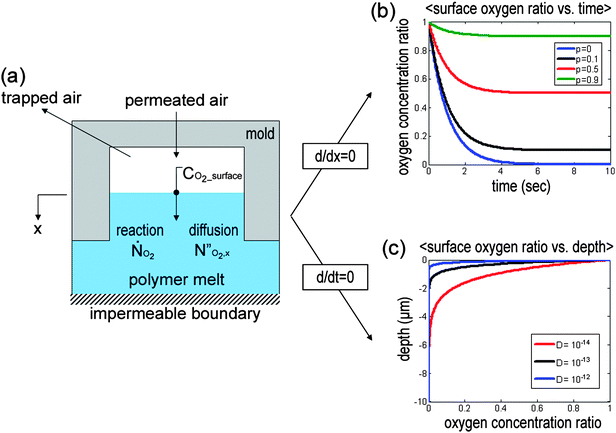 | ||
| Fig. 6 (a) Schematic illustration of permeation, diffusion and homogenous chemical reaction of oxygen in the polymer resin. (b) Change of oxygen concentration within the cavities as a function of time for micropatterned moulds with different permeability (k = 1). (c) Plot of the oxygen concentration with three different diffusivities of oxygen into the PUA resin (DPUA = 10−13–10−12 m2 s−1). As shown, oxygen concentration decreases exponentially in the x-direction, so that there is essentially no oxygen present approximately below about 4–5 µm. | ||
To gain an understanding of the oxygen concentration inside the mould cavity with time, which is associated with the permeability of the mould, a one-dimensional kinetic equation for oxygen can be derived by neglecting oxygen diffusion into the polymer layer in eqn (1), yielding
 | (2) |
Integration of eqn (2) then gives
 | (3) |
In addition to the time variation of oxygen concentration, the spatial change of oxygen also should be considered to understand the depth of the partial curing layer. For this purpose, one can derive a first-order diffusion equation for oxygen into the polymer layer by assuming steady-state conditions from eqn (1):
 | (4) |
This differential equation is easily solved in the dimensionless form with respect to the surface concentration of oxygen, CO2_surface (x = 0):
 | (5) |
2.4 Applications of two-step UV-assisted CFL
Among many possible applications, the current method would be especially useful to create nature-inspired, multiscale hierarchical surfaces. It has been revealed that elaborate functionalities of natural materials come from macro/micro/nanoscale combined hierarchical structures.13,43–47 One such example is a gecko lizard, which exhibits strong, yet reversible adhesion capability against surfaces of varying roughness and orientation due to their hierarchically organized foot hairs. Gecko foot hairs are comprised of a hierarchical structure of arrays of millions of fine microscopic foot hairs (setae), splitting into hundreds of smaller, nanoscale ends (spatulae), which form intimate contacts with various surfaces by van der Waals forces with strong adhesion (∼10 N cm−2).43,48 The gecko's multiscale combined hierarchical structures maximize structural compliance and thus increase adhesion strength against a rough surface with varying amplitude and wavelength without the structural instability observed in high AR nanostructures.49–51As a result, a number of methods have been proposed to mimic gecko's multiscale, hierarchical hairs. For generating hierarchical structures, multi-step photolithography,52 modified soft lithography,51 MEMS processing53 and direct moulding from AAO templates54 have been proposed. However, several challenges remain such as low resolution, low adhesion and structural instability, which significantly compromise the adhesion performance of the engineered surfaces.
In this light, the two-step UV-assisted CFL technique can be directly utilized to fabricate gecko-like high-aspect-ratio hierarchical hairs by overcoming the aforementioned limitations. For fabricating a microscopic setae-like structure, a micropatterned PDMS mould was placed onto a drop-dispensed UV-curable PUA resin on a thin PET film substrate followed by partial curingvia exposure to UV light for 50 s. Fabrication of spatulae-like, slanted nanohairs on the preformed microstructure was subsequently carried out by applying a nanoscale PUA mould. As mentioned previously, a partially cured microstructure can be further moulded by sequential application of a nanopatterned mould with the aid of inhibitory effects of trapped or permeated oxygen within cavities at the mould–polymer interface, resulting in a monolithic hierarchical structure.
Fig. 7a–b shows SEM images of multiscale hierarchical PUA hairs on a thin PET film substrate. As shown in the figure, well-defined angled, high AR nanohairs with a protruding flat head were uniformly formed on top of 5 µm hairs (spacing of 5 µm, height of 25 µm) over a large area without collapse of the underlying microstructures. It is intriguing that these structures appear similar to the actual gecko foot hairs. One notable feature is that the nanohairs have bulged flat heads similar to gecko's spatulae, which maximizes the contact area and thus adhesion force. As a consequence, the nanohairs could generate strong adhesion force (∼26 N cm−2) against a flat surface.2 Another important feature is that the nanohairs are angled. Fabrication of slanted nanohairs is essential for anisotropic, reversible dry adhesion because an angled structure significantly lowers the effective modulus of the surface. More importantly, anisotropic adhesion properties (i.e., strong attachment and easy detachment) could be obtained with slanted structures since such surfaces are only adhesive when loaded in a particular direction. For fabricating angled nanohairs, which are formed over the underlying microhairs, a new angled etching technique has recently been developed by employing a Faraday cage.2 In this process, the combination of angled etching and replica moulding resulted in the monolithic integration of slanted nanohairs on the microhairs with precise control over geometrical parameters (size, length, leaning angle and tip shape).
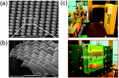 | ||
| Fig. 7 (a) A SEM image of tilted gecko-inspired hierarchical PUA hairs formed over a large area and (b) magnified, tilted images of (a), showing well-defined high AR, and angled nanohairs with bulged flat tops formed on 5 µm pillars (5 µm spacing, 25 µm height). (c) A photograph of the LCD glass transport system (top) and a magnified photograph showing the dry-adhesive patch integrated with the system (bottom). Reproduced from ref. 2. | ||
These monolithic, multiscale structures are especially useful for an artificial dry adhesive since they can enhance structural integrity and mechanical strength without an interface failure under an external load. With their structural similarity to gecko foot hairs, the hierarchical hairs maintained their adhesive force even on a rough surface (roughness <20 µm) due to an increase in the contact area by the enhanced height of hierarchy, whereas simple nanohairs lost their adhesion strength, demonstrating the usefulness of hierarchical structures against rough surfaces.2 Moreover, the multiscale hairs exhibit a directional adhesion property (strong attachment and weak detachment) due to the slanted nanohairs formed over the base microhairs. Based on the directional adhesion characteristic, it was revealed that the hierarchical nanohairs can be utilized for transporting a large-area glass panel without surface contamination (Fig. 7c), demonstrating potential applications of the adhesive patch with angled hierarchical nanohairs.
Another example of a bio-inspired multiscale functional surface is a lotus leaf, which exhibits amazing superhydrophobic properties due to dual-scale hierarchical structures on its surface.44 According to previous studies, the construction of micro/nanoscale hierarchical structures is a prerequisite to preparing a surface with the superior wetting properties of a higher contact angle (CA) and a lower sliding angle.55 To this end, it is possible to fabricate micro/nano dual roughness structures by using the two-step UV-assisted CFL technique and examine the wetting properties of a water droplet on the surface. Fig. 8a shows dual roughness surfaces consisting of microstructures (40 µm boxes with spacing of 80 µm and height of 40 µm) combined with 300 nm nanolines on top (spacing of ∼600 nm, height of ∼300 nm). For surface hydrophobization, the patterned surfaces were treated with trichloro(1H,1H,2H,2H-perfluorooctyl)-silane. The contact angle (CA) on a silane-treated flat PUA surface was measured to be ∼110°.
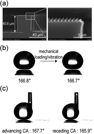 | ||
| Fig. 8 (a) A dual roughness structure with 300 nm lines (600 nm spacing, 300 nm height) over a 40 µm box pattern (80 µm spacing, 40 µm height). (b) Static contact angles on hierarchical structures before (left) and after (right) applying a mechanical loading or vibration. (c) Advancing and receding contact angles on hierarchical structures. Reprinted from ref. 32. | ||
The CA on the patterned microstructures or nanostructures was ∼125.2° and 146.2°, respectively. In contrast, the addition of nanostructures on the microstructures gave rise to an increased CA of ∼166.8°, which exhibited superhydrophobicity as compared to a simple micro- or nanostructured surface (Fig. 8b). Furthermore, the water droplet hardly adhered to the dual roughness surface, whereas it adhered easily to the microstructured surfaces. The droplet was also stable such that the Cassie wetting state was maintained even under mechanical loading or vibration. Moreover, the contact angle hysteresis (CAH) on the dual roughness surface was measured to be ∼2° (Fig. 8c), whereas that on the simple microstructured surface was over 30°, indicating that hierarchical structures are essential for realizing a stable Cassie state as well as an enhancement of CA and small CAH.32
In addition to applications that aim to mimic the bio-inspired functional properties of surfaces, the current method may also be of benefit for microfluidic chips or lab-on-a chip devices. One example is a microfluidic particle filter for precise collection of nanoparticles. To fabricate such a particle filtering device, we fabricated suspended nanomesh structures (hole size: 400 nm) over a microline structure (width of 20 µm and spacing of 20 µm) by the same method under low vacuum conditions. After fabricating the suspended nanomesh structures, a solution drop containing a mixture of 200 nm and 490 nm polystyrene particles was directly drop-dispensed on the structures. Fig. 9a shows motion of a droplet containing mixed nanoparticles after dispensing. When a solution of mixed particles is dispensed on the suspended nanomesh, the droplet starts to penetrate into the mesh holes due to its gravity and capillarity, and then moves laterally along the underlying microline structures by capillary action. To measure the trajectory of the nanoparticles during this process, the nanoparticles were tagged with different fluorescent dyes (green for 200 nm and red for 490 nm particles) and visualized under a fluorescence microscope. As shown in Fig. 9b–c, red-fluorescent nanoparticles that were larger than the mesh holes were trapped on the suspended meshes; whereas green-fluorescent nanoparticles passed through the meshes and were then collected on the underlying microstructures. Although more work is necessary to further analyze and optimize this process, this result demonstrates the possibility that the hierarchical, suspended bridge structures presented here can be used for a variety of other applications in microfluidic devices.
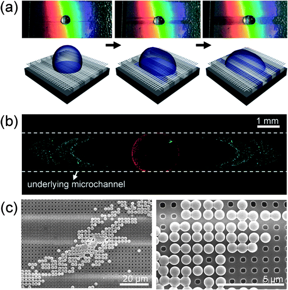 | ||
| Fig. 9 (a) Motion and schematic illustration with three consecutive steps of a droplet containing mixed particles with red (diameter of 490 nm) and green fluorescent polystyrene beads (diameter of 200 nm) on a suspended mesh structure (width of 450 nm, space of 450 nm and height of 500 nm) formed over the underlying microline structures (width of 20 µm, space of 20 µm and height of 13 µm). (b) A fluorescence image after dropping a liquid droplet. While red-fluorescent particles (490 nm diameter) remain on the mesh due to their larger size than that of mesh hole, green-fluorescent particles (200 nm diameter) are detected under the suspended mesh structures. | ||
3. Conclusions
This feature article has presented an overview of the two-step UV moulding technique for fabricating well-defined hierarchical structures containing both nano- and microstructures in a fast and geometrically-controllable manner. The method is based on sequential application of the UV-assisted CFL process using microscale and nanoscale moulds in two steps. A key finding is that a partially cured microstructure can be further moulded by subsequent application of a nanopatterned mould on the top surface, resulting in the formation of a monolithic, hierarchical structure and various nanoscale bridge structures.32,33,38The multiscale structures have shown great potential as a tool to mimic nature's multiscale functional surfaces such as gecko foot hairs2 and lotus leaves.5,32,38 Micro/nanoscale hierarchical structures are considered to be optimized building blocks that are mostly found in nature. Therefore, the fabrication of multiscale hierarchical structures may be a powerful tool for developing biomimetic functional surfaces. Also, it was found that various hierarchical nanobridge structures can be fabricated with high pattern fidelity and structural integrity, which could be useful for cell culture substrate and microfluidic applications.33
Recently, we found that in addition to PUA resin, other UV-curable materials such as polyethylene glycol dimethacrylate (PEG-DMA), polyethylene glycol diacrylate (PEG-DA), Norland Optical Adhesive (NOA, Norland Products), and even CNT-, silver- or gold nanoparticle-containing UV-curable resins can be used for the patterning material, and produce similar multiscale structures. With increasing demands on complex, hierarchically ordered structured interfaces, the two-step UV-assisted CFL technique presented here would serve as a new fabrication tool for a variety of applications including biomimetic , bio, micro/nanofluidic, photonic and electronic devices.
Acknowledgements
This work was supported by the Korea Science & Engineering Foundation through the Nano R&D Program (Grant 2007-02605), the King Abdullah University of Science and Technology (KAUST) program (No. KUK-F1-037-02) and the Micro Thermal System Research Center at Seoul National University.References
- E. Arzt, S. Gorb and R. Spolenak, Proc. Natl. Acad. Sci. U. S. A., 2003, 100, 10603–10606 CrossRef CAS.
- H. E. Jeong, J. K. Lee, H. N. Kim, S. H. Moon and K. Y. Suh, Proc. Natl. Acad. Sci. U. S. A., 2009, 106, 5639–5644 CrossRef CAS.
- Y. Xiu, L. Zhu, D. W. Hess and C. P. Wong, Nano Lett., 2007, 7, 3388–3393 CrossRef CAS.
- L. Feng, S. H. Li, Y. S. Li, H. J. Li, L. J. Zhang, J. Zhai, Y. L. Song, B. Q. Liu, L. Jiang and D. B. Zhu, Adv. Mater., 2002, 14, 1857–1860 CrossRef CAS.
- H. E. Jeong, S. H. Lee, J. K. Kim and K. Y. Suh, Langmuir, 2006, 22, 1640–1645 CrossRef CAS.
- S. L. Wu, X. M. Liu, T. Hu, P. K. Chu, J. P. Y. Ho, Y. L. Chan, K. W. K. Yeung, C. L. Chu, T. F. Hung, K. F. Huo, C. Y. Chung, W. W. Lu, K. M. C. Cheung and K. D. K. Luk, Nano Lett., 2008, 8, 3803–3808 CrossRef CAS.
- W. Hu, E. K. F. Yim, R. M. Reano, K. W. Leong and S. W. Pang, J. Vac. Sci. Technol., B, 2005, 23, 2984–2989 CrossRef CAS.
- S. S. Liao, F. Z. Cui, W. Zhang and Q. L. Feng, J. Biomed. Mater. Res., 2004, 69b, 158–165 Search PubMed.
- J. Han and H. G. Craighead, Science, 2000, 288, 1026–1029 CrossRef CAS.
- G. Chen, G. T. McCandless, R. L. McCarley and S. A. Soper, Lab Chip, 2007, 7, 1424–1427 RSC.
- J. O. Tegenfeldt, C. Prinz, H. Cao, R. L. Huang, R. H. Austin, S. Y. Chou, E. C. Cox and J. C. Sturm, Anal. Bioanal. Chem., 2004, 378, 1678–1692 CrossRef CAS.
- H. Cao, J. O. Tegenfeldt, R. H. Austin and S. Y. Chou, Appl. Phys. Lett., 2002, 81, 3058–3060 CrossRef CAS.
- A. R. Parker and H. E. Townley, Nat. Nanotechnol., 2007, 2, 347–353 CrossRef CAS.
- J. Henzie, M. H. Lee and T. W. Odom, Nat. Nanotechnol., 2007, 2, 549–554 CrossRef CAS.
- M. A. S. Chong, Y. B. Zheng, H. Gao and L. K. Tan, Appl. Phys. Lett., 2006, 89, 233104 CrossRef.
- J. A. Rogers, M. Meier, A. Dodabalapur, E. J. Laskowski and M. A. Cappuzzo, Appl. Phys. Lett., 1999, 74, 3257–3259 CrossRef CAS.
- J. Y. Lao, J. G. Wen and Z. F. Ren, Nano Lett., 2002, 2, 1287–1291 CrossRef CAS.
- C. H. Ye, L. D. Zhang, X. S. Fang, Y. H. Wang, P. Yan and J. W. Zhao, Adv. Mater., 2004, 16, 1019 CrossRef CAS.
- Y. T. Tseng, W. H. Tseng, C. H. Lin and R. M. Ho, Adv. Mater., 2007, 19, 3584 CrossRef CAS.
- Y. H. Xiu, L. B. Zhu, D. W. Hess and C. P. Wong, Langmuir, 2006, 22, 9676–9681 CrossRef CAS.
- Q. D. Xie, G. Q. Fan, N. Zhao, X. L. Guo, J. Xu, J. Y. Dong, L. Y. Zhang, Y. J. Zhang and C. C. Han, Adv. Mater., 2004, 16, 1830 CrossRef CAS.
- H. Y. Erbil, A. L. Demirel, Y. Avci and O. Mert, Science, 2003, 299, 1377–1380 CrossRef CAS.
- S. H. Li, H. J. Li, X. B. Wang, Y. L. Song, Y. Q. Liu, L. Jiang and D. B. Zhu, J. Phys. Chem. B, 2002, 106, 9274–9276 CrossRef CAS.
- H. Liu, J. Zhai and L. Jiang, Soft Matter, 2006, 2, 811–821 RSC.
- G. W. Meng, Y. J. Jung, A. Y. Cao, R. Vajtai and P. M. Ajayan, Proc. Natl. Acad. Sci. U. S. A., 2005, 102, 7074–7078 CrossRef CAS.
- N. Kehagias, V. Reboud, G. Chansin, M. Zelsmann, C. Jeppesen, C. Schuster, M. Kubenz, F. Reuther, G. Gruetzner and C. M. S. Torres, Nanotechnology, 2007, 18, 175303 CrossRef.
- X. D. Huang, L. R. Bao, X. Cheng, L. J. Guo, S. W. Pang and A. F. Yee, J. Vac. Sci. Technol., B, 2002, 20, 2872–2876 CrossRef CAS.
- J. Zaumseil, M. A. Meitl, J. W. P. Hsu, B. R. Acharya, K. W. Baldwin, Y. L. Loo and J. A. Rogers, Nano Lett., 2003, 3, 1223–1227 CrossRef CAS.
- S. Jeon, E. Menard, J. U. Park, J. Maria, M. Meitl, J. Zaumseil and J. A. Rogers, Adv. Mater., 2004, 16, 1369–1373 CrossRef CAS.
- L. R. Bao, X. Cheng, X. D. Huang, L. J. Guo, S. W. Pang and A. F. Yee, J. Vac. Sci. Technol., B, 2002, 20, 2881–2886 CrossRef CAS.
- F. X. Zhang, J. Chan and H. Y. Low, Appl. Surf. Sci., 2008, 254, 2975–2979 CrossRef CAS.
- H. E. Jeong, R. Kwak, J. K. Kim and K. Y. Suh, Small, 2008, 4, 1913–1918 CrossRef CAS.
- R. Kwak, H. E. Jeong and K. Y. Suh, Small, 2009, 5, 790–794 CrossRef CAS.
- S. Johnson, R. Burns, E. K. Kim, G. Schmid, M. Dickey, J. Meiring, S. Burns, N. Stacey, C. G. Willson, D. Convey, Y. Wei, P. Fejes, K. Gehoski, D. Mancini, K. Nordquist, W. J. Dauksher and D. J. Resnick, J. Photopolym. Sci. Technol., 2004, 17, 417–419.
- C. Decker and A. D. Jenkins, Macromolecules, 1985, 18, 1241–1244 CrossRef CAS.
- K. Studer, C. Decker, E. Beck and R. Schwalm, Prog. Org. Coat., 2003, 48, 92–100 CrossRef CAS.
- P. Tiemblo, J. Guzman, E. Riande, E. F. Salvador and C. Peinado, J. Polym. Sci., Part B: Polym. Phys., 2001, 39, 786–795 CrossRef CAS.
- H. E. Jeong, S. H. Lee, P. Kim and K. Y. Suh, Colloids Surf., A, 2008, 313–314, 359–364 CrossRef.
- C. Decker, Macromol. Rapid Commun., 2002, 23, 1067–1093 CrossRef CAS.
- S. J. Choi, P. J. Yoo, S. J. Baek, T. W. Kim and H. H. Lee, J. Am. Chem. Soc., 2004, 126, 7744–7745 CrossRef CAS.
- H. E. Jeong, S. H. Lee, P. Kim and K. Y. Suh, Nano Lett., 2006, 6, 1508–1513 CrossRef CAS.
- H. E. Jeong and K. Y. Suh, Lab Chip, 2008, 8, 1787–1792 RSC.
- K. Autumn, Y. A. Liang, S. T. Hsieh, W. Zesch, W. P. Chan, T. W. Kenny, R. Fearing and R. J. Full, Nature, 2000, 405, 681–685 CrossRef CAS.
- C. Neinhuis and W. Barthlott, Ann. Bot., 1997, 79, 667–677 CrossRef.
- J. Aizenberg, J. C. Weaver, M. S. Thanawala, V. C. Sundar, D. E. Morse and P. Fratzl, Science, 2005, 309, 275–278 CrossRef CAS.
- K. Vallé, P. Belleville, F. Pereira and C. Sanchez, Nat. Mater., 2006, 5, 107–111 CrossRef CAS.
- P. Fratzl, J. R. Soc. Interface, 2007, 4, 637–642 CrossRef CAS.
- K. Autumn, M. Sitti, Y. C. A. Liang, A. M. Peattie, W. R. Hansen, S. Sponberg, T. W. Kenny, R. Fearing, J. N. Israelachvili and R. J. Full, Proc. Natl. Acad. Sci. U. S. A., 2002, 99, 12252–12256 CrossRef CAS.
- B. Bhushan, A. G. Peressadko and T. W. Kim, J. Adhes. Sci. Technol., 2006, 20, 1475–1491 CrossRef CAS.
- H. Yao and H. Gao, J. Mech. Phys. Solids, 2006, 54, 1120–1146 CrossRef.
- M. P. Murphy, S. Kim and M. Sitti, ACS Appl. Mater. Interfaces, 2009, 1, 849–855 Search PubMed.
- C. Greiner, E. Arzt and A. del Campo, Adv. Mater., 2009, 21, 479 CrossRef CAS.
- M. T. Northen and K. L. Turner, Sens. Actuators, A, 2006, 130–131, 583–587 CrossRef.
- T. S. Kustandi, V. D. Samper, W. S. Ng, A. S. Chong and H. Gao, J. Micromech. Microeng., 2007, 17, N75–N81 CrossRef CAS.
- H. E. Jeong, M. K. Kwak, C. I. Park and K. Y. Suh, J. Colloid Interface Sci., 2009, 339, 202 CrossRef CAS.
| This journal is © The Royal Society of Chemistry 2009 |
