Nanoscale optical imaging by atomic force infrared microscopy
James H.
Rice
*
School of Physics, University College Dublin, Belfield, Dublin, Ireland. E-mail: james.rice@ucd.ie
First published on 11th February 2010
Abstract
This review outlines progress in atomic force infrared microscopy, reviewing the methodology and its application in nanoscale infrared absorption imaging of both biological and functional materials, including an outline of where this emerging method has been applied to image cellular systems in aqueous environments.
 James H. Rice | James Rice received his BSc and PhD degrees from the University of Sussex and the Queen's University Belfast respectively. Following this he spent time applying and developing optical techniques to study nanomaterials at the Université Paris-Sud (Laboratoire Aimé Cotton), the University of Oxford (Clarendon Laboratory) and the University of East Anglia. James Rice became a member of staff of the School of Physics at UCD in 2008. |
1. Introduction
Optical microscopy is an important and widely used method of imaging a range of structures and processes in materials from semiconductors to biological cells. The resolution of optical microscopy has a physical limit, the diffraction limit.1,2 The maximum resolution in optical microscopy is found to be ca.λ/2. Diffraction imaging using electromagnetic radiation at 5 μm (corresponding to an infrared (IR) absorption frequency of 2000 cm−1) results in an image resolution of 2.5 μm. Diffraction means that optical microscopy technology cannot image on the nanoscale (i.e. an image resolution of one hundred nanometres or less), even in the blue region of the visible electromagnetic spectrum.3 As a consequence, the application of optical microscopy to the study of nanoscale functional materials or to emerging disciplines such as nanobiology is limited.A number of techniques however have been established that do enable imaging of both functional materials and biosystems on the nanoscale. Important among these are none-optical methods such as electron microscopy, atomic force microscopy (AFM) and X-ray spectroscopy. Electron microscopy techniques such as high-resolution transmission electron microscopy (HRTEM) enable imaging of materials with a resolution better than 1 nm. Electron microscopy is an established method used to investigate both functional materials and biological processes. This method enables both 2D and 3D imaging when using, for example, scanning electron microscope-based methods.4–6 While these methods are presently considered state-of-the-art techniques for imaging both functional and biomaterials they possess limitations in information about the chemical structure of the material under investigation in comparison to what is obtained using optical methods such as Raman or infrared (IR) spectroscopy. X-Ray photoelectron spectroscopy, and electrophoretic mobility measurements enable high-resolution studies of cell-surface properties, however these methods require cell manipulation prior to measurement and provide averaged information obtained on ensembles of cells.7–9 Atomic force microscopy (AFM) has nm spatial resolution, with the possibility of ambient and live cell imaging.10 While AFM provides detailed topography information, limited information in regard to the chemical composition of the material under inspection can be obtained. However methods such as chemical force microscopy enable AFM to chemical identify surface located species via the use of modified AFM probe tips.11 While this method is demanding, requiring the preparation of AFM tips with specifically chosen organic monolayers it is emerging as an important method to evaluate the chemical composition of in particular biosystems.
Far-field optical microscopy encompasses a large number of different techniques such as Raman, IR, absorption or fluorescence based methods. These methods are based on measuring light that is either transmitted or scattered from the sample, with the light either collected and/or delivered by a microscope objective. Advances in sub-diffraction imaging have been made for fluorescence based imaging. A number of fluorescence microscopy techniques have been developed to which overcome the diffraction limit such as stimulated emission depletion microscopy (STED) and photoactivated localization microscopy (PALM) and are increasingly applied to image both functional materials and biosystems.12 These sub-diffraction fluorescence imaging methods are currently among the state-of-the-art methods for sub-diffraction optical imaging. These methods, in common with other fluorescence imaging techniques, address specific fluorophore groups and are unable to detect non-luminescent materials present within a host system. To date, advances have been limited for other far-field optical microscopy methods such as Raman and absorption techniques. An alternative method to far-field optical microscopy is near-field optical techniques. This method enables imaging with a resolution well beyond the diffraction limit. Scanning near-field optical microscopy (SNOM) combines high-resolution scanning probe methods with optical spectroscopy to enable ultrahigh resolution optical microscopy imaging. In SNOM the near-field optical probe is typically 20–120 nm in diameter.13 This aperture forms the resolution limit which is much smaller than the wavelength of the excitation light, thus enabling sub-diffraction imaging. The generation of tips with such small apertures is demanding. The probe emits light that consists mostly of evanescent waves instead of propagating waves. As a result of this, the incident light interacts with the sample within a layer typical tens of nm from the probe i.e. in the ‘near-field’ region. This limits significantly the studies that can be performed using SNOM, typically confining this method to surface-related studies. In addition, as it is a scanning probe based method, using SNOM to study soft, rough and motile surfaces, such as living cells, is very challenging. However, SNOM has been applied successfully to study a wide range of functional materials and biological systems. This approach has been advanced to include advanced infrared imaging methods.14 Infrared NSOM operating without any external illumination has been demonstrated, making use of the thermal infrared evanescent fields emitted by the surface. This method is referred to as ‘thermal radiation scanning tunnelling microscopy’ and was applied to image thermally excited surface plasmons and demonstrate spatial coherence effects in near-field thermal emission.
Absorption microscopy has the potential to provide considerable information with regard to the chemical composition of both luminescent and non-luminescent materials.14 An extensively used form of absorption spectroscopy is infrared absorption (IR) spectroscopy. This method of absorption spectroscopy measures the absorption of light by materials in the infrared region of the electromagnetic (EM) spectrum. IR spectroscopy commonly utilises the region of the EM spectrum between 1.5–30 μm (4000–400 cm−1). In this region molecular materials absorb radiation via vibration transitions. This enables IR to measure specific frequencies at which constituent parts of molecules corresponding to specific types of molecular bonds vibrate. This makes possible structural elucidation and compound identification of materials. As a consequence, IR absorption is extensively used as a (bio)chemical analytical tool. IR absorption spectroscopy when applied to imaging provides a method of chemical imaging or chemical mapping. IR absorption spectroscopy can be achieved using a range of different experimental approaches such as FT-IR, photoacoustic IR, ATR-IR which use a range of radiation sources such as free-electron laser based sources, optical parametric oscillator (OPO) lasers, dye lasers or blackbody radiation.15–17 However, to date, when these approaches are applied to IR imaging the lateral spatial resolution (in the x and y Cartesian axes) is limited by diffraction to ca.λ/2. For IR absorption imaging this results in a spatial resolution on the micron length scale (>1 μm). This has limited the application of IR imaging.
In this review an emerging method is outlined, referred to as AFMIR, that enables IR imaging with lateral nanoscale resolution based on combining AFM and optical methodologies.
2. Infrared absorption imaging based on combining atomic force microscopy and optical techniques
Atomic force microscopy (AFM) enables topographic imaging of surfaces with very high spatial resolution, i.e. <10 nm.18 Scattering near-field microscopy (SNIM) is based on the detection of scattered light from an oscillating antenna i.e. an AFM cantilever tip to enable optical imaging with high lateral resolution.19–25 This method uses a vibrating metallic AFM cantilever tip, which periodically and locally modifies the electromagnetic field distribution of the excitation laser which has been focused to a diffraction limited spot size. SNIM however recovers an optical resolution better than the diffraction limit. In addition SNIM simultaneously generates a reflection-mode near-field optical image and a tapping-mode AFM image, enabling the sample to be studied mapped independently by topography and optical methodologies.SNIM can achieve a spatial resolution of λ/100. SNIM in the infrared has been applied to study heterogeneous sample surfaces under ambient conditions. Several soft and hard condensed matter systems have been studied, including cells and tissues. For example SNIM has been demonstrated in the wavelength region near 6 μm covered by a line-tuneable CO laser to obtain a lateral resolution of <20 nm.22 This approach has been use to obtain infrared spectra of single individual poly(methyl methacrylate) nanobeads and viruses at nanoscale resolution (i.e. a lateral resolution of <20 nm). However, due to factors such as the elastic light scattering mechanism and the complex dielectric value of the sample SNIM absorption measurements are approximations of optical absorption measurements.19–22 Albeit with this limitation in recovering IR absorption information, SNIM IR imaging has been applied to image a number of systems with a spatial resolution of tens of nm.22 SNIM has been applied to image functional materials such as insulator-to-metal transition in vanadium dioxide thin films.23 This study probed directly percolative insulator–metal transitions with temperature. In addition to studying biological and functional inorganic materials SNIM has been applied to image functional organic systems such as microstructured self-assembled monolayers, imaging with a lateral resolution of 90 nm24 The authors estimated that this method could chemical image 27 attogram or 30![[hair space]](https://www.rsc.org/images/entities/char_200a.gif) 000 molecules. SNIM is been continuously developed, an example of this is work is evaluating the efficiency of back-scattering-based SNIM using a standard cantilever AFM probe contacting a flat sample and by applying a coherent frequency-comb Fourier-transform method.25
000 molecules. SNIM is been continuously developed, an example of this is work is evaluating the efficiency of back-scattering-based SNIM using a standard cantilever AFM probe contacting a flat sample and by applying a coherent frequency-comb Fourier-transform method.25
A separate method to SNIM which also combines AFM and optical methods has been developed, referred to as photothermal IR microscopy. Hammiche et al. demonstrated that IR spectra of analytes and thin films could be recorded by combining a Fourier transform infrared spectroscopy instrument with an AFM, a technique referred to as photothermal IR microscopy.26,27 This approach is based on an opto-thermal method that utilizes specific AFM probes as temperature sensors enabling measurements of opto-thermal signals induced by absorption of IR radiation enabling in turn measurements of IR absorption as a consequence photothermal IR microscopy does not require that the AFM tip be in contact with the sample surface.28,29 This method has been applied to image a number of biological systems. Building on this work Dazzie et al. demonstrated a method of IR microscopy referred to as atomic force microscopy infrared microscopy (AFMIR) that enables IR imaging with sub-wavelength lateral resolution. AFMIR combines optics and AFM. IR imaging occurs by using the AFM cantilever as the optical detector enabling high resolution imaging.30,31 This method measures IR absorption directly via measuring local transient deformation in the AFM cantilever induced by an infrared pulsed laser tuned at a vibrational absorbing wavelength (as outlined below). As a consequence, this method is related to photothermal IR microscopy. AFMIR enables IR imaging and simultaneous AFM topography with a spatial resolution on the nanoscale. This review will now concentrate on outlining in detail AFMIR and its applications to date.
3. Atomic force microscopy infrared microscopy (AFMIR)
3.1. AFMIR's detection mechanism
AFMIR measures directly IR absorption with nanoscale lateral resolution by using an AFM cantilever as the optical detector. AFMIR does this in the following way. The AFM cantilever tip is positioned over the sample with the tip in contact with the sample surface. Following the application of the IR radiation source the cantilever response is monitored. Specifically a change in vertical displacement of the tip following irradiation of the sample is monitored (see Fig. 1). This displacement arises from absorption of the incident radiation. Following absorption of the incident radiation, the sample disperses the absorbed energy via thermal and acoustic mechanisms. Propagating acoustic shock fronts induce a vertical displacement of the AFM tip. In order to record an absorption IR spectrum measurement of the tip displacement intensity as a function of wavelength is undertaken. As the incident laser excitation wavelength is tuned into resonance with an absorption transitions of the sample (such as the C–H stretch at ca. 3.5μm) the displacement intensity increases as it reaches the maximum of the absorption transition, thereafter it will reduce as the excitation wavelength is tuned past the maximum of absorption. In this way an IR absorption spectrum can be recorded. IR imaging then is performed by monitoring the cantilever intensity as a function of AFM tip position as well as a function of excitation wavelength. Dazzi et al. demonstrated that in contact mode the cantilever vibration modes enables amplification of very small distortions induced by laser absorption enabling measurements of surface deformation normally too small to be measured.30,31 The authors demonstrated that the cantilever oscillates at resonant frequencies, the amplitudes of which can be correlated with local absorption, allowing this system to act as an amplifier of extremely small motions induced by optical absorption. The rapid vertical displacement of the AFM tip from the surface deformation causes the tip to oscillate or vibrate. This vibration in the AFM tip is measured on timescales that precede the time response of the feedback loop. The AFM is operated in contact mode, with a typical setpoint of the tip between 5 and 10 nN. The type of cantilever can be important. The presence of metallic coatings can affect the degree of laser absorption by the tip which effects the background signal. The spring constant of the cantilever will affect the sensitivity of the measurement system, were it is anticipated that a small spring constant is desired as this will enable smaller absorption intensities to be measured potentially. Through analysis of the force curve of the contact and by establishing the set-point, the AFM can remain in a linear range in contact with the surface. AFM topography and IR images are recorded simultaneously which enables two different data sets to be collected and superimposed together to provide information on chemical composition and surface profile. | ||
| Fig. 1 Schematic drawing of (a) the cantilever and sample before and after absorption of radiation, shown is the surface deformation effects creating displacement in the position of the cantilever following excitation (left), a graph of the intensity of the resulting cantilever oscillations over time following excitation (right). (b) The ATR-based AFMIR setup which uses a free-electron laser, (c) top-down experimental setup which uses a table-top PPLN-based laser system. | ||
3.2. Experimental methodology
Two different experimental methods have been demonstrated for AFMIR. Standard AFMIR utilises an optical excitation arrangement based on attenuated total internal reflection (ATR). The second experimental method is surface AFMIR referred to here as s-AFMIR which uses direct excitation of the sample surface via a top-down excitation arrangement.4. Application of AFMIR and s-AFMIR to IR imaging of biological and functional materials
AFMIR has been applied to a number of different systems to date. We shall start by reviewing where AFMIR has been applied to study biological systems and then where AFMIR has been applied to study functional materials.4.1. Biological systems: cells, bacteria and viruses
A study of a single fixed Escherichia coli (E. coli) bacteria deposited onto an ATR prism substrate surface was undertaken.30,31 Imaging the surface features of a single E. coli was achieved simultaneously with AFM topography and IR with a spatial resolution of <100 nm. Localised IR spectra of E. coli were recorded using AFMIR and compared with the spectrum of an assembly of bacteria (measured with a far-field FTICR spectrometer) which showed the same features. AFMIR was then applied to study E. coli bacteria infected with T5 phage (bacteria virus).34 Bacteria E. coli was grown in Lysogeny broth media to the exponential growth phase and infected by phages, where the virus infection was studied at various stages using AFMIR. Single T5 phages were studied as dried samples at two different wavelengths, at 1650 cm−1 (amide I) characterizing the proteins of the capsid and at 1080 cm−1, the maximum absorption of the DNA band. These studies indicated that IR images of a single T5 phages could only be obtained at 1650 cm−1. IR imaging at the amide I band produced poor IR images as proteins constitute only a small fraction of the phage head, which is mainly constituted of DNA, the authors demonstrated that when imaging was performed at 1080 cm−1 the IR image is blurred compared to the topography indicating that the phages have been damaged arising from denaturing of the virus following drying leading to DNA breakdown. When the T5 phages were prepared infecting the bacteria IR imaging were performed in resonance with the DNA absorption band in order to detect the presence of the virus as no denaturing of the virus DNA occurs within the bacteria. Dazzi et al. studied three stages of infection. Fig. 2 shows AFM topography images that were recorded of the bacterium along with the corresponding IR images of these three stages of infection. These studies indicated that the virus concentration and location could be identified within the bacteria using AFMIR with a resolution of ca. 100 nm. The authors noted that single viruses could be identified within the bacteria.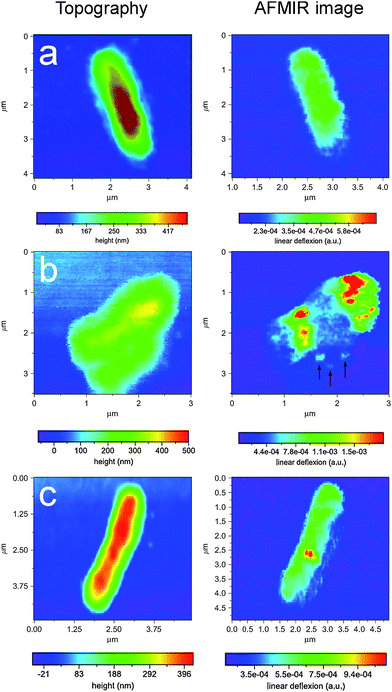 | ||
| Fig. 2 Study of a single Escherichia coli bacteria and T5 phage bacteria virus. AFMIR chemical mapping images recorded at 1080 cm−1 of three stages of infection. (a) non-infection, (b) heavily infected, and (c) only one phage visible. Reproduced with permission from ref. 34. Copyright Elsevier 2007. | ||
AFMIR has been applied to image live cells. Studies of live Candida albicans fungi cells were performed by Mayet et al.35 Studies were performed using the ATR excitation alignment. This experimental arrangement reduces IR light propagation into the surrounding water environment which in turn reduces sample heating and thus minimizing sample perturbation. Blastospore and Hyphea candida albicans fungi were studied in water. These systems were studied between 800–1200 cm−1 in order to assess the water window. IR imaging was performed at the glycogen band centred at 1080 cm−1. The resulting IR images indicated that the glycogen band is distributed uniformly. Water absorption was shown to occur with significant strength from 900 to 800 cm−1, while relatively low water absorption occurred between 900 to 1200 cm−1. Simultaneous AFM images and IR images were recorded (see Fig. 3) enabling cross confirmation of images profiles. Comparing these images showed that the intensity of the glycogen band signal in the IR image matches the AFM topography image profile for each sample studied. These studies demonstrated that the AFM cantilever vibration in water could be measured and IR imaging was possible. Effects arising from the water environment on the measured vibrations from the cantilever were reported but these effects, arising from friction forces etc., while present, did not preclude imaging. The authors showed that Fourier technique analysis enables the contribution of the sample from the surrounding absorbing medium to be resolved. Studies of water absorption were also made, showing that the wavelength window of imaging was required to be carefully chosen in order to avoid strong water absorption transitions. The authors reported that the spatial resolution seems identical in liquid to that in air at ca. 100 nm. This study demonstrated that live cell imaging can be performed using AFMIR albeit within a specific spectral region (i.e. the water window).
 | ||
| Fig. 3 Candida albicans fungi cell left, hyphae and right, blastospore immersed in water. (a) and (c) AFM topography, (b) and (d) AFMIR images at 1080 cm−1. Reproduced with permission from ref. 35. Copyright Optical Society of America 2009. | ||
4.2. Self-assembled quantum dots and inorganic microstructures
The spectral measurement of the absorption of quantum dots has been reported for visible and near-infrared wavelengths in resonance with interband transitions involving electron and hole pairs, however measurements of intraband transitions in single quantum dots is challenging. AFMIR has been successfully applied to measure single quantum dot absorption in the mid-infrared spectral range at room temperature.36 Houel et al. applied AFMIR to study intraband transitions in single n-doped InAs/GaAs self-assembled quantum dots which were prepared with a 20 nm capping layer. Charged self-assembled quantum dots with electrons (or holes) can undergo inter-sublevel absorption transitions between discrete confined levels which typically occur at mid- or far-infrared energies depending on the properties of the quantum dot probed. AFMIR was applied to InAs/GaAs self-assembled quantum dots which were of ca. 20 nm in width and ca. 4 nm in height, exhibiting inter-sublevel transitions between 8–20 μm at room temperature. A weak absorption cross-section estimated at 3 × 10⁻⁹ for a resonant inter-sublevel transition at 10 μm was reported which overlaps with background ambient blackbody radiation. Measurements of intra-sublevel transitions in single quantum dots at 9.6 μm using AFMIR have been undertaken.36 The authors measured in resonance with intraband transition of a single charge between discrete confined levels originating from the conduction band, specifically the observed absorption was assigned to arise from two S–D bound-to-bound inter-sublevel absorptions. The intensity of these absorptions was recorded as a function of AFM tip position, enabling imaging. Mapping of the quantum dots was performed at 9.6 μm with a spatial resolution of λ/150 i.e. 60 nm. Fig. 4 shows the AFM topography, AFMIR images and theoretical calculations obtained in this study. Fig. 4(b) shows the AFMIR image for a sample with a specific doping concentration where the white colour corresponds to the IR absorption signature of single quantum dots. The authors noted that only a small fraction of the quantum dots can be observed in the image among the ca. 250 quantum dots statistically buried under the surface. This was suggested to arise from the fact that all the quantum dots are not significantly populated at room temperature as a result of the balance between carrier capture and thermionic emission. In addition only a fraction of the quantum dots exhibit absorption that is spectrally resonant with the laser wavelength (as supported by theoretical calculations outlined in Fig. 4 which match with experimental data). Furthermore the authors noted that larger spots in Fig. 4(b) can be seen attributed to a gathered group of several dots which cannot be spatially resolved. Fig. 4(c) shows an AFMIR image of a quantum dot with a reduced charge population, which shows less image features while Fig. 4(d) shows the AFMIR spectrum for a highly charged quantum dot sample showing increased image features. This study demonstrated that imaging with very high lateral spatial resolution (i.e. 60 nm) can be archived with AFMIR. In addition AFMIR can be applied to image sub-surface features with the quantum dots imaged by Houel et al. present 20 nm below a semiconductor capping layer.36 | ||
| Fig. 4 Study of quantum dots, (a) AFM topography image of the quantum dot sample, (b) corresponding AFMIR image of a quantum dot sample with nominal modulation doping of 4 × 1011 cm−2 recorded at 9.6 mm noting that the quantum dots appear with a bright colour. *c) and (d) AFMIR images of two other quantum dot samples with nominal modulation doping of 4 × 1010 cm−2 and of 4 × 1012 cm−2 respectively. Reproduced with permission from ref. 36. Copyright American Physical Society 2003. | ||
IR bulk GaAs phonon absorption and IR absorption of thin SiO2 microdisks were studied using AFMIR by Houel et al.37 AFMIR imaging was performed with a lateral spatial resolution achieved with microdisks of around 50 nm. AFMIR imaging followed the spectral dependence of the bulk absorption. The measurements on bulk GaAs and on SiO2 microdisks deposited on silicon showed that both surface and bulk contribute to the signal. This was interpreted by the authors to indicate that both the acoustic and thermal propagation of the deformation plays an important role, which can lead to phase delays and can induce a decrease of the oscillation amplitude of the cantilever.
4.3. Polymer micostructures
s-AFMIR has been applied by Hill et al. to image soft matter systems, specifically microscale polystyrene beads.32To date this is the only application of s-AFMIR in the literature. IR absorption and AFM topography images of polystyrene beads were recorded simultaneously with an image resolution of 200 nm. Chemical maps were reported at 3000 cm−1 in transition with the C–H stretch of the poly(styrene) system. Local IR spectroscopy was performed by placing the tip over a poly(styrene) bead (in contact mode) and scanning the excitation wavelength while keeping the tip stationary. The local spectrum with a spatial resolution of ca. 200 nm was thus recovered (shown in Fig. 5). This spectrum compared well with a FTIR sample of poly(styrene) film. IR images recorded at the absorption maxima at ca. 2925 cm−1 (position α) and not in resonance with an IR absorption band at 2800 cm−1(position β). Fig. 5. Shows the IR absorption image recorded at the C–H vibration frequency (position α as outlined in Fig. 5d) and away from it (position β as outlined in Fig. 5) respectively, plus the AFM topographic image. The IR absorption image recorded on the absorption peak shows an object that absorbs intensely (light colouring) present on a nonabsorbing (dark) background. The position and extent of the IR absorbing object matches the AFM topography image. This study demonstrated that direct surface excitation of the sample enables AFMIR imaging.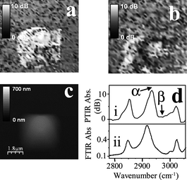 | ||
| Fig. 5 Study of poly(styrene), (a), Topography AFM image, (b) on-resonance absorption image and (c) off-resonance absorption image. (d) Spectra showing (i) AFMIR response (ii) and FTIR response of poly(styrene) to IR. Reproduced with permission from ref. 32. Copyright Optical Society of America 2001. | ||
5 Discussion and conclusion
A range of methods exist for IR imaging such as photoacoustic IR microscopy or synchrotron infrared microspectrometry, however the spatial resolution of these approaches is limited by diffraction to λ/2.14–17,38–44 Resulting in the lateral IR image resolution limited to the micron lengthscale. The use of attenuated total internal reflection (ATR) methodology however provides a method to provide enhanced vertical spatial resolution by utilizing evanescent waves to probe samples studying samples on the order of the evanescent waves penetration depth i.e. on the order of λ.38–40 ATR does not improve the lateral spatial resolution which is critical for surface imaging in particular.Alternative methods of vibrational spectroscopy imaging to IR methods exist. Raman microscopy has been able to provide high spatial resolution spectroscopic imaging via the use of small λ (via EM radiation in the near-UV) and confocal methodologies, matching the spatial resolution of fluorescence microscopy. While in theory it is possible to continuously improve the spatial resolution of Raman microscopy via the use of higher excitation frequencies into the UV and higher (soft X-ray region etc.), it has been found that excitation of notable biosystems at such high excitation energies produces fluorescence which ‘drowns’ the Raman signal. This has effectively resulted in the lateral resolution of Raman microscopy remaining above the nanoscale. In contrast, the spatial resolution of AFMIR is determined ultimately by the AFM cantilever profile. This has enabled imaging with 60 nm lateral resolution (at a wavelength of 10 μm resulting in an image resolution of λ\150). Raman imaging and established IR imaging methods are limited to λ\2 by the Abbe limit. Near-field approaches have been demonstrated that enable IR and Raman spectroscopy imaging to be performed. These approaches utilise optical apertures, plasmon enhancement effects and/or tip oscillations methods to enable imaging. However such approaches are not able to recover IR absorption information which in contrast to Raman spectroscopy, being a scattering technique, can be recovered successfully.41
The application of AFMIR to biological systems has been demonstrated by probing bacterium and living cells (as outlined above). These studies demonstrated that soft matter i.e. biological systems can be probed using AFMIR and, significantly, that living systems can be studied using this method. It is noted that the presence of water, which is a strong IR absorber limits the spectral window in the IR and as a consequence limits the potential of this method to chemical map living biosystems. In contrast to this, other spectroscopic imaging methods such as Raman are not so limited by the presence of water and can potentially probe a wider spectral window. Studies of biosystems to date performed using AFMIR include both live and fixed cells. The study of fixed cells has centred on characterising the occurrence of specific functional groups on the samples surface. These studies have reported homogeneous distribution of specific chemical functional groups, i.e. the amide I band or the glycogen band. However, when probing relatively large features such as viruses within a host organism,34 the power of AFMIR becomes apparent demonstrating that in order to utilise this method to its full potential AFMIR should be applied to systems that have inhomogeneous distributions of material. A second example of this is the study of quantum dot materials embedded within a wider band gap host via probing intra-subband transitions.36
Present AFMIR technology has been expanded to include to two experimental methodologies, ATR and direct-surface excitation, enabling a wide range or samples to be mapped with high lateral resolution. It is noted however, that such mapping is limited in the Z-plane. Studies of virus in bacteria demonstrated that viruses present beneath the host surface can be imaged but with undefined resolution.34 Presently the inability to resolve information in the Z-plane is a limit in the imaging ability of AFMIR.
Future potential applications of AFMIR could extend to areas such as in mechanical studies of materials. It is noted that AFM-TIRFM based experimental system can observe mechanical processes such as stress transmission in cells.45 AFMIR may in the future be applied to study such processes by varying the AFM cantilever’s downward force on the system under study and then recovering the IR data. Other future applications of AFMIR may be combining this method with other techniques to form a single hybrid instrument, thereby achieving potentially enhanced understanding of molecular processes such as morphological or mechanical based processes. This may be achieved by combining AFMIR with other spectroscopic methods, mechanical or electrochemical techniques.
In conclusion, AFMIR enables local spectroscopy or chemical mapping of materials with nanoscale resolution simultaneously with AFM topography imaging. The lateral image resolution of AFMIR being on the nanoscale. This approach combines atomic force microscopy and an infrared pulsed laser. This nano-tool has been applied to enable local IR spectroscopy (utilising a stationary AFM tip) or chemical imaging (utilising a scanning AFM tip) of biomaterials, organic polymer systems and semiconductor materials. AFMIR imaging can be applied to systems in aqueous environments demonstrating that live cell bio-imaging can be undertaken within the IR water window.
References
- E. Hecht, Optics, Addison and Wesley, Reading, MA, 3rd edn, 1998 Search PubMed.
- E. Abbe, Arch. Mikrosk. Anat., 1873, 9, 413–420 Search PubMed.
- S. W. Hell, Nat. Biotechnol., 2003, 21, 1347–1355 CrossRef CAS.
- P. Walther, High Resolution Cryoscanning Electron Microscopy of Biological Samples in Biological Low-Voltage Scanning Electron Microscopy, Springer-Verlag, New York, 2008 Search PubMed.
- R. Egerton, Physical principles of electron microscopy, Springer, New York, 2005 Search PubMed.
- Y. Shao-Horn, L. Croguennec, C. Delmas, E. C. Nelson and M. A. O'Keefe, Nat. Mater., 2003, 2, 464–467 CrossRef.
- F. Verni, S. Gabrielli, From Cells to Proteins: Imaging Nature across Dimensions, vol. 3, Springer, Netherlands, 2006 Search PubMed.
- J. Ubbink and P. Schar-Zammaretti, Micron, 2005, 36, 293–320 CrossRef CAS.
- N. Mozes, P. S. Handley, H. J. Busscher, P. G. Rouxhet, Microbial Cell Surface Analysis: Structural and Physicochemical Methods, VCH Publishers, New York, 1991 Search PubMed.
- B. P. Jena, J. K. Heinrich-Horber, L. Wilson, P. T. Matsudaira, Atomic Force Microscopy in Cell Biology, Academic PressLondon, 2002 Search PubMed.
- Y. F. Dufrêne, Nat. Protoc., 2008, 3, 1132–1138 Search PubMed.
- J. H. Rice, Mol. BioSyst., 2007, 3, 781–793 RSC.
- B. Hecht, B. Sick, U. P. Wild, V. Deckert, R. Zenobi, O. J. F. Martin and D. W. Dieter, J. Chem. Phys., 2000, 112, 7761–7774 CrossRef CAS.
- Y. De Wilde, F. Formanek, R. Carminati, B. Gralak, P. A. Lemoine, K. Joulain, J. P. Mulet, Y. Chen and J. J. Greffet, Nature, 2006, 444, 740–743 CrossRef CAS.
- A. J. McQuillan, Adv. Mater., 2001, 13, 1034–1038 CrossRef.
- H. F. Zhang, K. Maslov, G. Stoica and L. V. Wang, Nat. Biotechnol., 2006, 24, 848–851 CrossRef CAS.
- K. Nishikida, E. Nishio, R. W. Hannah, Applications of Modern FT-IR Techniques, Kodanska Ltd with Gordan and Breach Publishing, Toyko, 1985 Search PubMed.
- T. R. Albrecht and C. F. Quate, J. Vac. Sci. Technol., A, 1988, 6, 271–274 CrossRef CAS.
- R. Bachelot, P. Gleyzes and C. Boccara, Opt. Lett., 1995, 20, 1924 Search PubMed.
- B. Knoll and F. Keilmann, Nature, 1999, 399, 134 CrossRef CAS.
- S. C. Kehr, M. Cebula, O. Mieth, T. Hartling, J. Seidel, S. Grafstrom, L. M. Eng, S. Winnerl, D. Stehr and M. Helm, Phys. Rev. Lett., 2008, 100, 256403 CrossRef CAS.
- M. Brehm, T. Taubner, R. Hillenbrand and F. Keilmann, Nano Lett., 2006, 6, 1307 CrossRef CAS.
- M. M. Qazilbash, 1. M. Brehm, G. O. Andreev, A. Frenzel, P.-C. Ho, B.-G Chae, B.-J. Kim, S. J. Yun, H.-T. Kim, A. V. Balatsky, O. G. Shpyrko, M. B. Maple, F. Keilmann and D. N. Basov, Phys. Rev. B: Condens. Matter Mater. Phys., 2009, 79, 075107 CrossRef.
- I. Kopf, J. Sebastien, S. Go1tz Wollny, C. Grunwald, E. Bru1ndermann and M. Havenith, J. Phys. Chem. C, 2007, 111, 8166–8171 CrossRef CAS.
- M. Brehm, A. Schliesser, F. Čajko, I. Tsukerman and F. Keilmann, Opt. Express, 2008, 16, 11203 CrossRef CAS.
- A. Hammiche, M. H. Pollock, M. Reading, M. Claybourn, P. M. Turner and K. Jewkes, Appl. Spectrosc., 1999, 53, 810–815 CrossRef CAS.
- A. Hammiche, L. Bozec, M. J. German, J. M. Chalmers, N. J. Everall, G. Poulter, M. Reading, D. B. Grandy, F. L. Martin and H. M. Pollock, Spectrosc., 2004, 19, 20–24 Search PubMed.
- A. Hammiche, L. Bozec, H. M. Pollock, M. German and M. Reading, J. Microsc., 2004, 213, 129–134 CrossRef CAS.
- M. Reading, D. M. Price, D. B. Grandy, R. M. Smith, L. Bozec, M. Conroy, A. Hammiche and H. M. Pollock, Macromol. Symp., 2001, 167, 45–62 CrossRef CAS.
- A. Dazzi, R. Prazeres, F. Glotin and J. M. Ortega, Infrared Phys. Technol., 2006, 49, 113–121 CrossRef CAS.
- A. Dazzi, R. Prazeres, F. Glotin and J. M. Ortega, Ultramicroscopy, 2007, 107, 1194–1200 CrossRef CAS.
- G. Hill, J. H. Rice, S. R. Meech, P. Kuo, K. Vodopyanov and M. Reading, Opt. Lett., 2009, 34, 431–433 Search PubMed.
- K. L. Vodopyanov and P. G. Schunemann, Opt. Lett., 2003, 28, 441–443 Search PubMed.
- A. Dazzi, R. Prazeresa, F. Glotina, J. M. Ortegaa, M. Al-Sawaftaha and M. de Frutos, Ultramicroscopy, 2008, 108, 635–641 CrossRef CAS.
- C. Mayet, A. Dazzi, R. Prazeres, F. Allot, F. Glotin and J. M. Ortega, Opt. Lett., 2008, 33, 1611–1614 Search PubMed.
- J. Houel, S. Sauvage, P. Boucaud, A. Dazzi, R. Prazeres, F. Glotin, J.-M. Ortega, A. Miard and A. Lemaıtre, Phys. Rev. Lett., 2007, 99, 217404 CrossRef.
- J. Houel, E. Homeyer, S. Sauvage, P. Boucaud, A. Dazzi, R. Prazeres and J. M. Ortega, Opt. Express, 2009, 17, 10887–10894 CrossRef CAS.
- L. G. Tisinger and A. J. Sommer, Microsc. Microanal., 2004, 10(s02), 1318–1319.
- K. L. A. Chan and S. G. Kazarian, Appl. Spectrosc., 2007, 61, 48–54 CrossRef CAS.
- P. Rullhusen, X. Artru, P. Dhez, Novel Radiation Sources Using Relativistic Electrons: From Infrared to X-rays (Series on Synchrotron Radiation Techniques & Applications), World Scientific Publishing Co Ltd, London, 1998 Search PubMed.
- D. Eichert, L. Gregoratti, B. Kaulich, A. Marcello, P. Melpignano, L. Quaroni and M. Kiskinova, Anal. Bioanal. Chem., 2007, 389, 1121–1132 CrossRef CAS.
- H. U. Gremlich, B. Yan, Infrared and Raman Spectroscopy of Biological Materials, CRC Press. London, 2000 Search PubMed.
- H. H. Mantsch, D. Chapman, Infrared Spectroscopy of Biomolecules, Wiley Blackwell, London, 1996 Search PubMed.
- M. Micic, N. Klymyshyn and Y. D. Suh, J. Phys. Chem., 2003, 107, 1574–1584 Search PubMed.
- A. B. Mathur, G. A. Truskey and W. M. Reichert, Biophys. J., 2000, 78, 1725–1735 CrossRef CAS.
| This journal is © The Royal Society of Chemistry 2010 |