Asymmetric printing of molecules and zeolites on self assembled monolayers†
Nermin Seda
Kehr
*a,
Andreas
Schäfer
b,
Bart Jan
Ravoo
c and
Luisa
De Cola
*a
aPhysikalisches Institut and CeNTech, Westfälische Wilhelms-Universität Münster, Mendelstrasse 7, 48149, Münster, Germany. E-mail: decola@uni-muenster.de; seda@uni-muenster.de.; Fax: +49 (0)251 9802834; Tel: +49 (0)251 9802873
bNanoAnalytics GmbH, Heisenbergstr. 11, 48149, Münster, Germany
cOrganic Chemistry Institute and CeNTech, Westfälische Wilhelms-Universität Münster, Corrensstraße 40, 48149, Münster, Germany
First published on 28th January 2010
Abstract
Microcontact printing (mCP) is used to immobilize dyes and peptides asymmetrically, by a “peptide coupling” reaction, on monolayers of zeolite L crystals in the contact area between the stamp and the surface of the monolayer. Chemically patterned surfaces of monolayers of zeolite L crystals are obtained by using patterned stamps with different ink solutions. Additional printing of functionalized nano-objects on SAMs of zeolite L crystals is demonstrated.
Introduction
The construction of self assembled monolayers (SAMs) of molecules, nanoparticles (NPs), nanocrystals and other nanometre sized objects with a wide range of specific chemical and physical properties (optical, electrical, magnetic, chemical functionalization and chemical composition etc.)1 is important in nano- and bio-technology2,3e.g. for applications in lithography, sensing, diagnostics, molecular electronics and biologically active surfaces.4–8 The large surface area of SAMs of nanomaterials provides a large number of contact points which can be used for an effective binding to biological systems. The organization of the biomolecules on the SAMs is of great interest since information transfer between the surfaces and corresponding biological systems can occur and eventually be controlled.9,10 In addition to the physical properties, molecular surface functionalization of SAMs of nanomaterials offers a wide range of functionalities which open fascinating routes to the creation of surface-specific receptors.11One powerful technique to modify specific properties of surfaces, or SAMs, at the micro- and nanoscale is microcontact printing12 (mCP). This technique is based on the selective transfer of ink molecules from a microstructured elastomer stamp to a substrate in the contact area between the stamp and the substrate. mCP is frequently used to pattern a wide variety of SAMs of molecules13 and nano–micro objects on different substrates.5–7,14 Additionally this technique is very useful for chemical synthesis on surfaces in the nanoscale confinement between stamp and substrate (“microcontact chemistry”).12c Examples of microcontact chemistry include the production of imine by mCP of amine on aldehyde SAMs,15 synthesis of peptides by mCP of N-protected amino acids on amino SAMs16 or mCP of acetylenes e.g. alkyl functionalized sugar derivatives onto azido-terminated SAMs via Huisgen click chemistry17 on silicon oxide substrates.18
To the best of our knowledge, there are no examples in the literature of the use of mCP for chemical synthesis of nanomaterials on SAMs. Since the functionalization of nano–micro objects in solution requires many hours, a high reaction temperature, organic solvents and sometimes even toxic catalysts,19 the interesting question arises of whether other techniques (e.g. mCP) can be used to reduce the reaction times of functionalization of nano–micro objects, to provide mild reaction conditions and spatial control of the chemical reaction.
Here we report the chemical functionalization of the top side of disc-shaped zeolite L nanocrystals (approximately 1 μm in diameter and 250 nm in height) assembled on a glass surface with molecules which are binded covalently by using mCP. The choice of such micro/nano objects was dictated by the fact that zeolites are biocompatible, optically transparent, size tunable, porous crystalline alumino-silicates and in particular the L-type ones have all the channels oriented along one dimension.20–22 It is also important to note that the channel functionalization has already been reported in solution where both ends of the crystals are statistically functionalized.23 The selective modification of the topside of a zeolite L monolayer in solution with molecules which are bound electrostatically was also reported.24 The distance between two adjacent channels is 1.8 nm which would allow each channel to be functionalized with a chemical group leading to a spatial control of the functionalities. Furthermore, it has been recently shown that zeolites can be organized in monolayers on a silica substrate by chemical functionalization24,25 and their channels are perpendicular to the substrate. Recently, we have reported the possibility of patterning disc-shaped zeolite L crystals on glass and indium tin oxide (ITO) and ITO/polymer using a transfer technique.6b
Zeolite SAMs were therefore selected for the above mentioned properties and in view of their rather flat exposed surface which could favour a homogenous functionalization by mCP.
In this contribution we describe for the first time the use of mCP for the functionalization of SAMs of disc-shaped zeolite L nanocrystals with biologically active molecules and fluorescent dyes (as a proof of principle for other molecules and ligands). As a step further we prove that the same technique can be applied for printing zeolites on a SAM of disc-shaped zeolite L nanocrystals. The assembly of flat objects on top of each other opens up a fascinating possibility for well oriented multilayer constructions of several micrometres in size.
Experimental section
Materials
3-Chloropropyl-trimethoxysilane (CP-TMS, 97%), ATTO-425 N-succinimidyl ester, arginine–glycine–aspartic acid (RGD), penicillamine (PEN), N-hydroxy-succinimide (NHS), N,N′-bis(2,6-dimethylphenyl)perylene-3,4,9,10-tetracarboxylic diimide (DXP) and thionine were purchased from Sigma-Aldrich. 3-(Aminopropyl)methoxydimethylsilane (APMS, 97%) was purchased from Acros, 9-fluorenylmethyl carbamate N-hydroxysuccinimidyl ester (FMOC-NHS) was purchased from Fluka. 1-Ethyl-3-(3-dimethylaminopropyl)carbodiimide (EDC) and polydimethylsiloxane (PDMS) were obtained from ABCR and Dow Corning Corporation (184 silicon elastomer base, SYLGARD) respectively. Toluene was purchased from Merck (stored over molecular sieves, puriss., H2O 0.005%). The glass plates (1.8 cm × 1.8 cm) used for zeolite L monolayers were obtained from Servoprax GmbH.General syntheses
Disc-shaped (approximately 1000 nm in diameter and 250 nm in height) zeolite L crystals were synthesized according to a well established literature procedure.26 The X-ray powder diffraction pattern of zeolite L is comparable with the literature results (for details see the ESI†).27 The crystal channel functionalization with 3-(aminopropyl)methoxy-dimethylsilane (APMS)23b and the loading of zeolite L crystals with DXP (N,N′-bis(2,6-dimethylphenyl)perylene-3,4,9,10-tetracarboxylic diimide) and thionine dyes were done according to literature methods.28 SAMs of amino functionalized zeolite on glass were prepared according to established protocols.25 In brief, amino functionalized zeolites (1 mg) and a 3-chloropropyltriethoxysilane tethered glass plate were sonicated for 20 min in toluene (1 ml).mCP of molecules on SAMs of zeolite L; general procedure
Striped polydimethylsiloxane (PDMS) elastomer stamps were prepared (50 μm and 10 μm striped stamps).6b The stamps were treated with air-plasma for 1 min before the printing process. The stamps were dipped for 2 min into a freshly prepared 1 mM solution of the respective ink molecule in ethanol. RGD and PEN solutions contain peptide coupling reagents EDC (10 mM) and NHS (10 mM) to activate the carboxylic acid group. The stamps were dried in a stream of argon and then placed with a tweezer on the SAMs of amino functionalized zeolite. After 30 min printing the stamps were removed; the substrate was vigorously rinsed with ethanol and dried in a stream of argon.Characterization
The morphology of the zeolite L monolayer was investigated using a Zeiss 1540 EsB dual beam focused ion beam/field emission scanning electron microscope (SEM) with a working distance of 8 mm and an electronic high tension (EHT) of 3 kV. Fluorescence microscopy was carried out with an Olympus BX-41 equipped with a Hg high pressure lamp. The FTIR spectrum was carried out with a Varian 3100 FT-IR Excalibur Series Spectrometer with Golden Gate ATR Accessory. XPS analysis has been done using an ESCALAB 250 from Thermo VG Scientific. Monochromatic Al Kα X-rays were used (15 kV, 150 W, ∼500 μm spot diameter). The transmission function of the analyzer had been calibrated using a standard copper sample. Spectra were measured using pass energy of 80 eV for survey spectra and 30 eV for core level spectra. Quantitative information about the surface composition is calculated from survey spectra using the standard Scofield sensitivity factors.29 XRD measurements were performed with an X-ray camera FR590 from Enraf Nonius with wavelength Cu Kα1 and an image plate reader BAS1800 from Fujitsu.Results and discussion
SAMs (Fig. 1) of amino functionalized zeolite on glass were prepared and dried under high vacuum at 60 °C for 18 h to eliminate as much as possible the water molecules entrapped in the channels of the zeolite L. To demonstrate the functionalization of the zeolite monolayer using mCP we have employed a fluorescent dye, ATTO-425, which, if covalent attached to the zeolites, after washing of the SAM, can be easily detected by confocal microscopy. The schematic procedure is depicted in Fig. 2.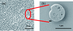 | ||
| Fig. 1 SEM image of SAMs of zeolite on glass (a); SEM image of disc-shaped zeolite crystal at higher magnification (b). | ||
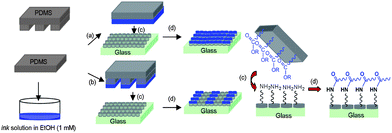 | ||
| Fig. 2 Schematic procedure for the design of non-patterned (a) and patterned (b) functionalization of zeolite L monolayers by microcontact printing (mCP); printing of ink molecule by PDMS stamps (c); formation of amide bond (d). | ||
For micro-contact printing, patterned and non-patterned PDMS were used as elastomeric stamps to print molecules to the top of the amino functionalized SAMs of zeolite L. The PDMS stamp was oxidized in ozone atmosphere to increase its wettability and ‘inked’ with a solution of NHS ester of ATTO-425 dye (1 mM in ethanol, λabs = 436 nm, λem = 484 nm). Subsequently, the PDMS stamp was dried and gently pressed onto the corresponding SAM of amino functionalized zeolite L surface. The soft PDMS stamp makes conformal contact with the surface and molecules are transferred directly from the stamp to the surface, resulting in the covalent amide bond formation. The stamp was contacted with the zeolite L SAM for 30 min. After that, the printed zeolite L monolayer was washed until the washing solution showed no detectable fluorescence emission, confirming that adsorbed dye (non covalently linked) has been removed and only covalently linked dye molecules remain at the zeolite SAM.
Fluorescence microscopy was used to verify the successful functionalization of the SAMs of zeolite L crystals with ATTO-425 dye by mCP. Fig. 3 shows fluorescence microscope images of the mCP experiments, using non-patterned (Fig. 3a and b) and patterned (Fig. 3c–f) PDMS stamps. The blue stripes, caused by the emission of the functionalized surface with the ATTO-425 dye molecules, are well defined over the entire zeolite monolayer.
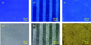 | ||
| Fig. 3 Fluorescence microscope images of ATTO-425 functionalized SAM of zeolite L on glass by mCP. Excitation in the region of 360–370 nm: non-patterned (a), patterned (50 μm–10 μm) (c and e). White light image: non-patterned (b), patterned (50 μm–10 μm) (d and f). | ||
This process can be extended to the use of two different dye molecules in order to functionalize the monolayers sequentially in different regions, perpendicular to each other, resulting in stripes of different colours (see Fig. 4). Two patterned PDMS stamps were oxidized in ozone atmosphere. One stamp was ‘inked’ with a solution of NHS ester of ATTO-610 dye (1 mM in ethanol, λabs = 615 nm, λem = 634 nm) and the other was ‘inked’ with NHS ester of ATTO-425 dye (1 mM in ethanol, λabs = 436 nm, λem = 484 nm). After drying both PDMS stamps, the first was pressed onto the SAM of amino functionalized zeolite L crystals. Subsequently, the second PDMS stamp was pressed onto the same zeolite L surface (rotated 90° relative to the first one) in such a way that the patterns combined to form a grid structure. The fluorescence microscopy image shows the expected well defined cross hatch of the functionalized patterned zeolite L monolayer with ATTO-610 and ATTO-425 dye molecules (Fig. 4).
 | ||
| Fig. 4 Schematic procedure for the sequential functionalization of the zeolite L monolayer in different regions, perpendicular to each other, by microcontact printing (mCP) (A); fluorescence microscopy image of ATTO-610 and ATTO-425 functionalized SAM of zeolite on glass by mCP (B). Excitation in the region of 360–370 nm. | ||
Since specifically functionalized SAMs of NPs have a high importance and applications in the field of bio- and nano-technologies, the mCP of ATTO dyes on SAMs of zeolites prove that molecules can be covalently linked in patterned nano-objects. This strategy can be extended to other types of molecules and in particular to bioactive molecules such as proteins, sugars, peptides etc. We have selected, as a proof of principle, a biologically active short chain peptide, [arginine–glycine–aspartic acid (RGD)] and an amino acid [L-penicillamine (PEN)] as candidates for the printing on SAMs of zeolite L, applying the same approach employed in the case of ATTO-425 dye.
Attenuated total reflection infrared (ATR-IR) spectroscopy and X-ray photoelectron spectroscopy (XPS) were used as an analytical technique to characterize the functionalization of the zeolite monolayers and to prove the formation of amide bonds during the chemical reaction between amino functionalized zeolite L monolayers and NHS ester of ATTO-425 dye, RGD and PEN inked PDMS stamps, respectively. The bands at ν = 1639, 1645, 1650 and 1548, 1554, 1547 cm−1 belong to amide bonds of ATTO-425-, RGD- and PEN-functionalized zeolite L monolayers which are characteristic of amide I and amide II absorptions (Fig. 5). The comparison of these spectra with those of SAM of amino functionalized zeolite L clearly shows the formation of the amide bonds. We conclude that mCP of the NHS ester of ATTO-425 dye, RGD and PEN on SAMs of amino functionalized zeolite L resulted in a peptide-type coupling reaction.
Additionally, XPS has been used to characterize the functionalization of the zeolite L monolayers by peptide coupling. Fig. 6 and Fig. 7 show the C1s and N1s spectra of amino (NH2), ATTO-425, RGD and PEN functionalized SAMs of zeolite L, respectively. These data are in agreement with results reported in the literature.30
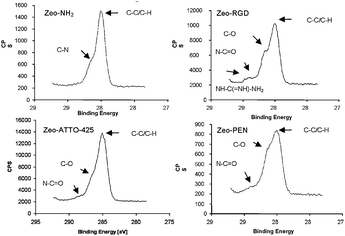 | ||
| Fig. 6 C1s XPS spectra of amino (NH2), ATTO-425, RGD and PEN functionalized SAMs of zeolite. | ||
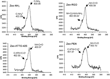 | ||
| Fig. 7 N1s XPS spectra of amino (NH2), ATTO-425, RGD and PEN functionalized SAMs of zeolite. | ||
In particular the XPS spectra of the SAMs of zeolite L (zeo-NH2, zeo-ATTO-425, zeo-RGD, zeo-PEN) display a sharp C1s peak at 285.0 eV as expected for a hydrocarbon chain containing mainly C–C and C–H bonds. The binding energy around 286.0 eV and 286.7 eV are assigned to amino (CH2N) and alkoxy groups (CH2O) respectively. C1s energies of the amide functions (O![[double bond, length as m-dash]](https://www.rsc.org/images/entities/char_e001.gif) C–N) are expected around 288.0 eV. The peak at a binding energy of about 289.2 eV is attributed to guanidine (in the case of RGD) [NH–C(=NH)–NH2] carbons (Fig. 6; for details see the ESI†).
C–N) are expected around 288.0 eV. The peak at a binding energy of about 289.2 eV is attributed to guanidine (in the case of RGD) [NH–C(=NH)–NH2] carbons (Fig. 6; for details see the ESI†).
In addition, the N1s XPS spectra confirm such results. All modified surfaces show two peaks (with different ratios) at ca. 400.1 eV (free amino groups or amide bonds) and 402.0 eV (H-bonded and/or positively charged amines). Amino functionalized SAMs of zeolite L surface shows two peaks at 400.6 eV due to free amino groups and at 402.0 eV, most probably owing to ammonium species (RNH3+). ATTO-425-, RGD- and PEN-functionalized zeolite monolayer surfaces show the increase of the high binding energy peaks at 402.0 eV, clearly due to the more positively charged nitrogen species in the guanidine fragment (in the case of RGD) and the interaction of the amino nitrogen with the carboxyl group of the amide bond (Fig. 7).
In addition to printing molecules on SAMs of zeolite L crystals, using mCP, we were also able to transfer a patterned SAM of functionalized zeolite L crystals by mCP on another layer of zeolites. A batch of the disc-shaped zeolite L crystals (approximately 1000 nm in diameter and 250 nm in height) were loaded with yellow-light-emitting DXP (N,N′-bis(2,6-dimethylphenyl)perylene-3,4,9,10-tetracarboxylic diimide) dye, and another sample of the same type zeolites were loaded with red-light-emitting thionine dye.28 Subsequently, the DXP- and thionine-dye-loaded zeolite L crystals were functionalized (separately) with APMS. Then for both sets of zeolites the corresponding SAMs on glass were made. Simultaneously, two striped patterned PDMS stamps (width ca. 50 μm) were prepared. One was pressed on the top of the DXP-dye-loaded zeolite L monolayer, the other one was pressed on the top of the thionine-dye-loaded zeolite L monolayer. After 20 s both stamps were peeled off carefully. The peeled striped patterned stamps picked up the corresponding modified zeolite L crystals from the glass surfaces leaving on the glass substrate the emitting patterned monolayer of zeolites loaded with DXP and thionine, respectively. PDMS was also patterned with the emitting zeolites as a negative replica of the substrate. At this point the patterned PDMS stamp carrying DXP loaded zeolite L crystals was used as ink for mCP on the glass supported thionine loaded zeolites. The DXP loaded zeolite L crystals of the stamp were imprinted perpendicular to the stripes of the patterned SAM of thionine loaded zeolite L crystals on the glass surface (Fig. 8). As depicted in Fig. 8a the white light microscope image shows the expected grid structure on the glass surface. The fluorescence microscope image (Fig. 8b) shows the (near) perpendicular line structures of the two different dye loaded zeolite L patterns. It should be emphasized that at the junctions of the grid-like surface structure we were able to print nano objects on a layer of nano objects.
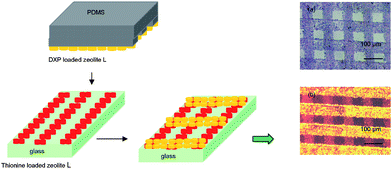 | ||
| Fig. 8 Printing of zeolite L crystals filled with DXP (yellow) on patterned zeolite L monolayers (filled with thionine, red) by mCP. White light image (a); fluorescence microscopy image (excitation in the region of 360–370 nm) (b). | ||
Conclusions
This work highlights the effective use of mCP for nanoscale chemical reactions on SAMs of zeolite L crystals. We have shown that different molecules (e.g. amino acids, peptides etc.) can easily be reacted with the surface of SAMs of zeolite L by mCP. Chemical functionalization occurs in the nanoscale confinement between the elastomeric stamp and the surface of zeolite L monolayer in minutes, under mild reaction conditions, without any organic solvents or catalyst. Patterned and chemically functionalized zeolite L monolayers were obtained by using patterned stamps. The application of mCP can be extended to other ink molecules (used for e.g. click chemistry, imine formation, thio click chemistry, Diels–Alder reaction etc.) for the functionalization of different SAMs of nanomaterials. Additionally, we have broadened these concepts to micro-sized objects, demonstrating the printing of zeolites on SAMs of zeolite L crystals. These last results open up a fascinating perspective on the use of mCP for materials of nano- and micrometre sizes.Acknowledgements
This work was partially supported by SFB TRR61 “806103”. We are grateful to Prof. Rainer Pöttgen and Dr Manfred Möller for XRD measurements.Notes and references
- A. P. Alivisatos, Science, 1996, 271, 933 CrossRef CAS; C. B. Murray, C. R. Kagan and M. G. Bawendi, Annu. Rev. Mater. Sci., 2000, 30, 545 CrossRef CAS; E. Granot, P. Fernando and I. Willner, J. Phys. Chem. B, 2004, 108, 5875 CrossRef CAS.
- C. Niemeyer, Angew. Chem., Int. Ed., 2001, 40, 4128 CrossRef CAS; E. Katz and I. Willner, Angew. Chem., Int. Ed., 2004, 43, 6042 CrossRef CAS.
- V. Zharov, P. Kim, D. T. Curiel and M. Everts, Nanomed.: Nanotechnol., Biol. Med., 2005, 1, 326 CrossRef CAS; T. Osaka, T. Matsunaga, T. Nakanishi, A. Arakaki, D. Niwa and H. Iida, Anal. Bioanal. Chem., 2006, 384, 593 CrossRef CAS.
- K. L. Prime and G. M. Whitesides, Science, 1991, 252, 1164 CrossRef CAS; C. S. Chen, M. Mrksich, S. Huang, G. M. Whitesides and D. E. Ingber, Science, 1997, 276, 1425 CrossRef CAS; B. T. Houseman, J. H. Huh, S. J. Kron and M. Mrksich, Nat. Biotechnol., 2002, 20, 270 CrossRef CAS.
- V. P. Pattani, C. Li, T. A. Desai and T. Q. Vu, Biomed. Microdevices, 2008, 10, 367 CrossRef CAS.
- (a) S. Li, Y. Yan, N. Liu, M. B. Chan–Park and Q. Zhang, Small, 2007, 3, 616 CrossRef CAS; (b) F. Cucinotta, Z. Popovic', E. A. Weiss, G. M. Whitesides and L. De Cola, Adv. Mater., 2009, 21, 1142 CrossRef CAS.
- D. Y. Khang, J. Xiao, C. Kocabas, S. MacLaren, T. Banks, H. Jiang, Y. Y. Huang and J. A. Rogers, Nano Lett., 2008, 8, 124 CrossRef CAS.
- X. Yan, J. Yao, G. Lu, X. Chen, K. Zhang and B. Yang, J. Am. Chem. Soc., 2004, 126, 10510 CrossRef CAS; Y. K. Kim, S. J. Park, J. P. Koo, G. T. Kim, S. Hong and J. S. Ha, Nanotechnology, 2007, 18, 015304 CrossRef.
- B. G. Trewyn, S. Giri, I. I. Slowing and V. S. Y. Lin, Chem. Commun., 2007, 3236 RSC; S. P. Hudson, R. F. Padera, R. Langer and D. S. Kohane, Biomaterials, 2008, 29, 4045 CrossRef CAS; Y. Jin, S. Lohstreter, D. T. Pierce, J. Parisien, M. Wu, C. Hall and J. X. Zhao, Chem. Mater., 2008, 20, 4411 CrossRef CAS.
- J. Park, S. Bauer, K. von der Mark and P. Schmuki, Nano Lett., 2007, 7, 1686 CrossRef CAS; L. Ferreira, J. M. Karp, L. Nobre and R. Langer, Cell Stem Cell, 2008, 3, 136 CrossRef CAS.
- A. K. Boal and V. M. Rotello, J. Am. Chem. Soc., 2000, 122, 734 CrossRef CAS; A. Verma and V. M. Rotello, Chem. Commun., 2005, 303 RSC.
- (a) A. Kumar and G. M. Whitesides, Appl. Phys. Lett., 1993, 63, 2002 CrossRef; (b) Y. Xia and G. M. Whitesides, Angew. Chem., Int. Ed., 1998, 37, 550 CrossRef CAS; (c) B. J. Ravoo, J. Mater. Chem., 2009, 19, 8902 RSC.
- N. L. Jeon, K. Finnie, K. Branshaw and R. G. Nuzzo, Langmuir, 1997, 13, 3382 CrossRef CAS; J. S. Hovis and S. G. Boxer, Langmuir, 2001, 17, 3400 CrossRef CAS; S. A. Lange, V. Benes, D. P. Kern, J. K. H. Horber and A. Bernard, Anal. Chem., 2004, 76, 1641 CrossRef CAS.
- P. C. Hidber, W. Helbig, E. Kim and G. M. Whitesides, Langmuir, 1996, 12, 1375 CrossRef CAS; V. Santhanam and R. P. Andres, Nano Lett., 2004, 4, 41 CrossRef CAS.
- D. I. Rozkiewicz, B. J. Ravoo and D. N. Reinhoudt, Langmuir, 2005, 21, 6337 CrossRef CAS; D. I. Rozkiewicz, Y. Kraan, M. W. T. Werten, F. A. de Wolf, Subramaniam, B. J. Ravoo and D. N. Reinhoudt, Chem.–Eur. J., 2006, 12, 6290 CrossRef CAS.
- P. Sullivan, M. L. van Poll, P. Y. W. Dankers and W. T. S. Huck, Angew. Chem., Int. Ed., 2004, 43, 4190 CrossRef CAS.
- R. Huisgen, Centenary Lecture – 1,3–Dipolar Cycloadditions, Proc. Chem. Soc. London, 1961, 357 RSC; R. Huisgen, Pure Appl. Chem., 1989, 61, 613 CrossRef CAS.
- O. Michel and B. J. Ravoo, Langmuir, 2008, 24, 12116 CrossRef CAS.
- Y. L. Liu, C. Y. Hsu, M. L. Wang and H. S. Chen, Nanotechnology, 2003, 14, 813 CrossRef CAS; K. Wojczykowski, D. Meißner, P. Jutzi, I. Ennen, A. Hutten, M. Fricked and D. Volkmere, Chem. Commun., 2006, 3693 RSC; A. P. Herrera, C. Barrera and C. Rinaldi, J. Mater. Chem., 2008, 18, 3650 RSC; Y. Li and B. C. Benicewicz, Macromolecules, 2008, 41, 7986 CrossRef CAS.
- S. M. Kanan, C. P. Tripp, R. N. Austin and H. H. Patterson, J. Phys. Chem. B, 2001, 105, 9441 CrossRef CAS; A. Corma and H. Garcia, Chem. Commun., 2004, 1443 RSC; V. R. Reddy, A. Currao and G. Calzaferri, J. Mater. Chem., 2007, 17, 3603 RSC.
- Z. Popovic, M. Otter, G. Calzaferri and L. De Cola, Angew. Chem., Int. Ed., 2007, 46, 6188 CrossRef CAS.
- C. Minkowski, R. Pansu, M. Takano and G. Calzaferri, Adv. Funct. Mater., 2006, 16, 273 CrossRef CAS; M. Busby, C. Blum, M. Tibben, S. Fibikar, G. Calzaferri, V. Subramaniam and L. De Cola, J. Am. Chem. Soc., 2008, 130, 10970 CrossRef CAS.
- (a) M. Busby, H. Kerschbaumer, G. Calzaferri and L. De Cola, Adv. Mater., 2008, 20, 1614 CrossRef CAS; (b) S. N. Huber and G. Calzaferri, Angew. Chem., Int. Ed., 2004, 43, 6738 CrossRef CAS.
- A. Z. Ruiz, H. Li and G. Calzaferri, Angew. Chem., Int. Ed., 2006, 45, 5282 CrossRef.
- K. B. Yoon, Acc. Chem. Res., 2007, 40, 29 CrossRef CAS; Z. Ming, Z. BaoQuan and L. XiuFeng, Chin. Sci. Bull., 2008, 53, 801 CrossRef CAS; J. S. Lee, K. Ha, Y. J. Lee and K. B. Yoon, Adv. Mater., 2005, 17, 837 CrossRef CAS.
- A. Z. Ruiz, D. Bruhwiler, T. Ban and G. Calzaferri, Monatsh. Chem., 2005, 136, 77 CrossRef CAS.
- S. Megelski and G. Calzaferri, Adv. Funct. Mater., 2001, 11, 277 CrossRef CAS.
- G. Calzaferri, S. Huber, H. Maas and C. Minkowski, Angew. Chem., Int. Ed., 2003, 42, 3732 CrossRef CAS.
- J. H. Scofield, J. Electron Spectrosc. Relat. Phenom., 1976, 8, 129 CrossRef CAS.
- S. J. Xiao, M. Textor, N. D. Spencer, M. Wieland, B. Keller and H. Sigrist, J. Mater. Sci.: Mater. Med., 1997, 8, 867 CrossRef CAS; S. S. Jedlicka, K. M. Little, D. E. Nivens, D. Zemlyanov and J. L. Rickus, J. Mater. Chem., 2007, 17, 5058 RSC.
Footnote |
| † Electronic supplementary information (ESI) available: Details of XPS spectra are given. See DOI: 10.1039/b9nr00285e |
| This journal is © The Royal Society of Chemistry 2010 |

